Embed Size (px)
Citation preview

1Lecture 1: Introduction & IC Yield
Spanos & PoollaEE290H F03
EE290H
Special Issues in Semiconductor Manufacturing
Costas J. SpanosDepartment of Electrical Engineering
and Computer Sciencesel (510) 643 6776, fax (510) 642 2739
email [email protected]
Kameshwar PoollaDepartment of Mechanical Engineering
el (510) 642 4642, fax (510) 643 5599email [email protected]
University of California Berkeley, CA 94720, U.S.A.
http://www-inst.eecs.berkeley.edu/~ee290h/
Fall 2003
2Lecture 1: Introduction & IC Yield
Spanos & PoollaEE290H F03
The purpose of this class
To integrate views, tools, data and methods towards a coherent view of the problem of Efficient Semiconductor Manufacturing.
The emphasis is on technical/engineering issues related to current state-of-the-art as well as future technology generations.

3Lecture 1: Introduction & IC Yield
Spanos & PoollaEE290H F03
The Evolution of Manufacturing Science1. Invention of machine tools. English system (1800).
mechanical - accuracy2. Interchangeable components. American system (1850).
manufacturing - repeatability3. Scientific management. Taylor system (1900).
industrial - reproducibility4. Statistical Process Control (1930).
quality - stability5. Information Processing and Numerical Control (1970).
system - adaptability6. Intelligent Systems and CIM (1980).
knowledge – versatility7. Physical and logical (“lights out”) Automation (2000).
integration – efficiency
4Lecture 1: Introduction & IC Yield
Spanos & PoollaEE290H F03
Fall 2003 EE290H Tentative Weekly Schedule
1. Functional Yield of ICs and DFM. 2. Parametric Yield of ICs.3. Yield Learning and Equipment Utilization.
4. Statistical Estimation and Hypothesis Testing.5. Analysis of Variance.6. Two-level factorials and Fractional factorial Experiments.
7. System Identification. 8. Parameter Estimation.9. Statistical Process Control. Distribution of projects. (week 9)
10. Run-to-run control.11. Real-time control. Quiz on Yield, Modeling and Control (week 12)
12. Off-line metrology - CD-SEM, Ellipsometry, Scatterometry13. In-situ metrology - temperature, reflectometry, spectroscopy
14. The Computer-Integrated Manufacturing Infrastructure
15. Presentations of project results.
ProcessModeling
ProcessControl
IC Yield & Performance
Metrology
ManufacturingEnterprise
5Lecture 1: Introduction & IC Yield
Spanos & PoollaEE290H F03
Bibliography• Introduction to Statistical Quality Control, D. C. Montgomery, John Wiley & Sons, 4th Edition, 2001• Design and Analysis of Experiments, D. C. Montgomery, John Wiley & Sons, 5th Edition, 2001• Manufacturing Yield Evaluation of VLSI/WSI Systems, Bruno Ciciani, IEEE Computer Society Press, 1995• Statistics for Experimenters, G.P. Box, W.G. Hunter, J.S. Hunter Wiley Interscience, 1978• Quality Engineering Using Robust Designs, Madhav S. Phadke, Prentice Hall 1989• Practical Experimental Designs for Engineers and Scientists, W. J. Diamond, Vannostrand & Reinhold, Second Edition,
1989• The Cartoon Guide to Statistics, L. Gonick & W. Smith, Harper Perennial, 1993• Guide to Quality Control, Kaoru Ishikawa Asian Productivity Organization - Quality Resources 1982• Quality Engineering in Production Systems, G. Taguchi, E. Elsayed, T. Hsiang, McGraw-Hill, 1989• Statistical Process Control in Automated Manufacturing, J. B. Keats and N.F. Hubele (editors) Marcel Dekker Inc. 1989• Statistical Methods for Industrial Process Control, D. Drain, Chapman and Hall, 1997• Special Issues in Semiconductor Manufacturing, Vols I-VI, Costas J. Spanos Electronics Research Laboratory EECS,
University of California, Berkeley, CA 94720• IEEE Transactions on Semiconductor Manufacturing, Quarterly publication of the IEEE.• Berkeley Computer-Aided Manufacturing Web site, http://bcam.eecs.berkeley.edu• Class Site http://www-inst.eecs.berkeley.edu/~ee290h/
• International Technology Road Map for Semiconductors, 2002 update http://public.itrs.net/• Atlas of IC Technologies - An Introduction to VLSI Processes, W. Maly, The Benjamin/Cummins Publishing Company,
Inc, 1987• Semiconductor Manufacturing (Draft MS) by Gary May and Costas Spanos.
6Lecture 1: Introduction & IC Yield
Spanos & PoollaEE290H F03
IC Yield and Performance• Defect Limited Yield
• Definition and Importance
• Metrology
• Modeling and Simulation
• Design Rules and Redundancy
• Parametric Yield• Parametric Variance and Profit
• Metrology and Test Patterns
• Modeling and Simulation
• Worst Case Files and DFM
• Equipment Utilization• Definition and NTRS Goals
• Measurement and Modeling
• Industrial Data
• General Yield Issues• Yield Learning
• Short loop methods and the promise of in-situ metrology
7Lecture 1: Introduction & IC Yield
Spanos & PoollaEE290H F03
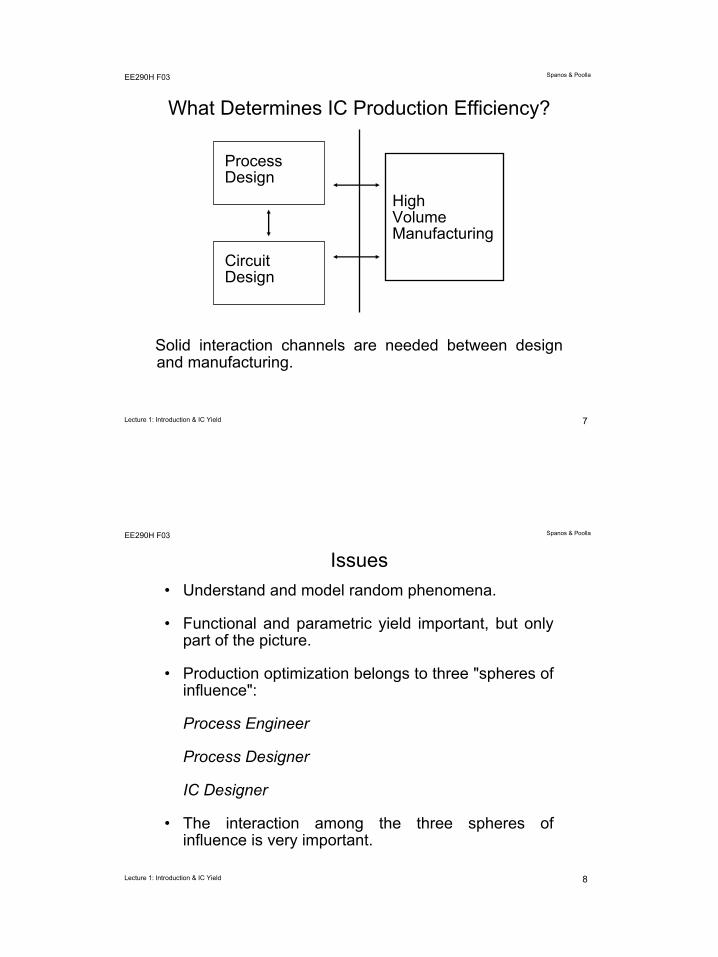
What Determines IC Production Efficiency?
Process Design
CircuitDesign
HighVolumeManufacturing
Solid interaction channels are needed between design and manufacturing.
8Lecture 1: Introduction & IC Yield
Spanos & PoollaEE290H F03
Issues• Understand and model random phenomena.
• Functional and parametric yield important, but only part of the picture.
• Production optimization belongs to three "spheres of influence":
Process Engineer
Process Designer
IC Designer
• The interaction among the three spheres of influence is very important.
9Lecture 1: Introduction & IC Yield
Spanos & PoollaEE290H F03
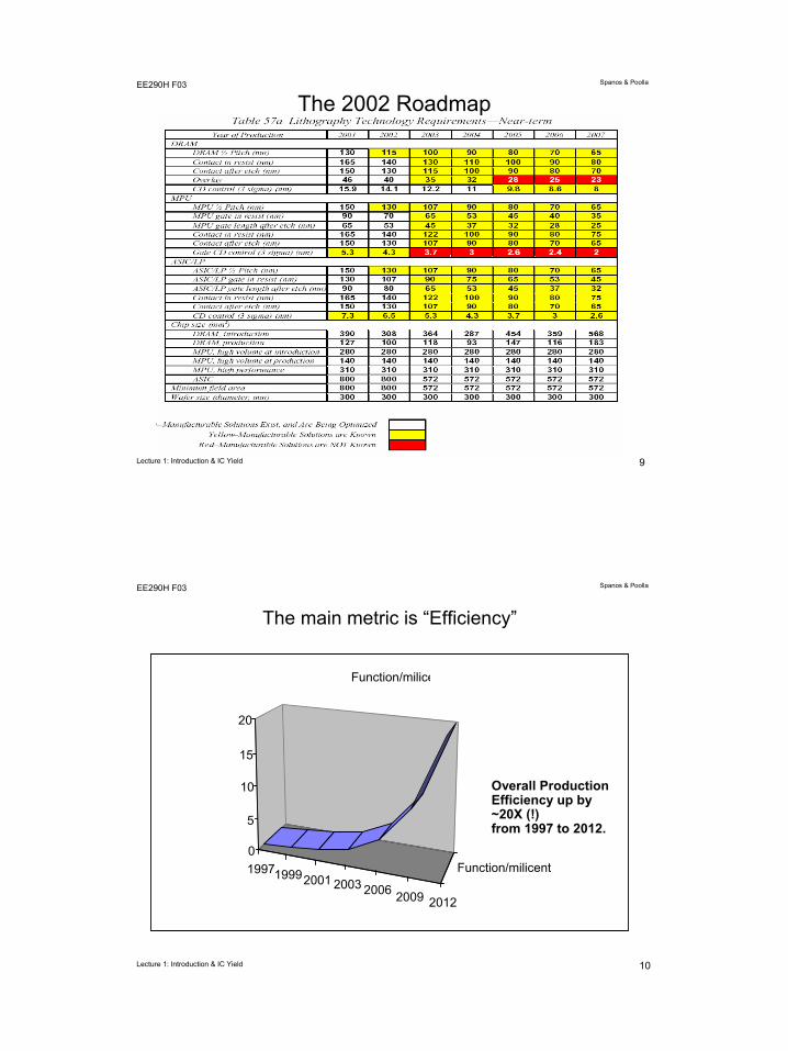
The 2002 Roadmap
10Lecture 1: Introduction & IC Yield
Spanos & PoollaEE290H F03
199719992001 2003 2006 2009 2012
Function/milicent0
5
10
15
20
Function/milice
Overall ProductionEfficiency up by ~20X (!) from 1997 to 2012.
The main metric is “Efficiency”

11Lecture 1: Introduction & IC Yield
Spanos & PoollaEE290H F03
Where will the Extra Productivity Come from?
(Jim Owens, Sematech)Time
Other Productivity - Equipment, etc.
Yield Improvement
Wafer Size
3%4%9%
12% Feature Size
12-14%
4%
7-10%2%
12-14%
<2%
<1%
9-15%Ln$
/ Fun
ctio
n
25% - 30% / Yr.Improvement
12Lecture 1: Introduction & IC Yield
Spanos & PoollaEE290H F03
The OpportunitiesYear 1997 1999 2001 2003 2006Feature nm 250 180 150 100 70Yield % 85 ~90 ~92 ~93 ?Equipment utilization % 35 ~50 ~60 ~70Test wafers % 5-15 5-15 5-15 5-15
OEE30%
Down Un15%Down Pl
3%No Prod7%
No Oper10%
Quality2%
Test Wafers8%
Setup10%
Speed15%

13Lecture 1: Introduction & IC Yield
Spanos & PoollaEE290H F03
Yield Definitions
• Yield is simply the percentage of “good” product in a production batch.
• Yield has several components, each requiring a distinct set of tools to understand and improve.
• We will talk about the three main components:– Functional (defect driven)– Parametric (performance driven)– Production efficiency / equipment utilization
14Lecture 1: Introduction & IC Yield
Spanos & PoollaEE290H F03
The Yield Problem• Improving Yield quickly used to be a key competitive
issue for all IC manufacturers.
• As the cost of installed equipment increases, one wants to amortize this cost over many ICs.
– Even on 24hour operation, equipment utilization is low.
– Limited yield is responsible for about 50% of equipment utilization loss.
– Yield fluctuations cause terrible planning problems.
– The problem is aggravated by frequent equipment, technology and design changes.
• One can say that Yield is limited by Variability
15Lecture 1: Introduction & IC Yield
Spanos & PoollaEE290H F03
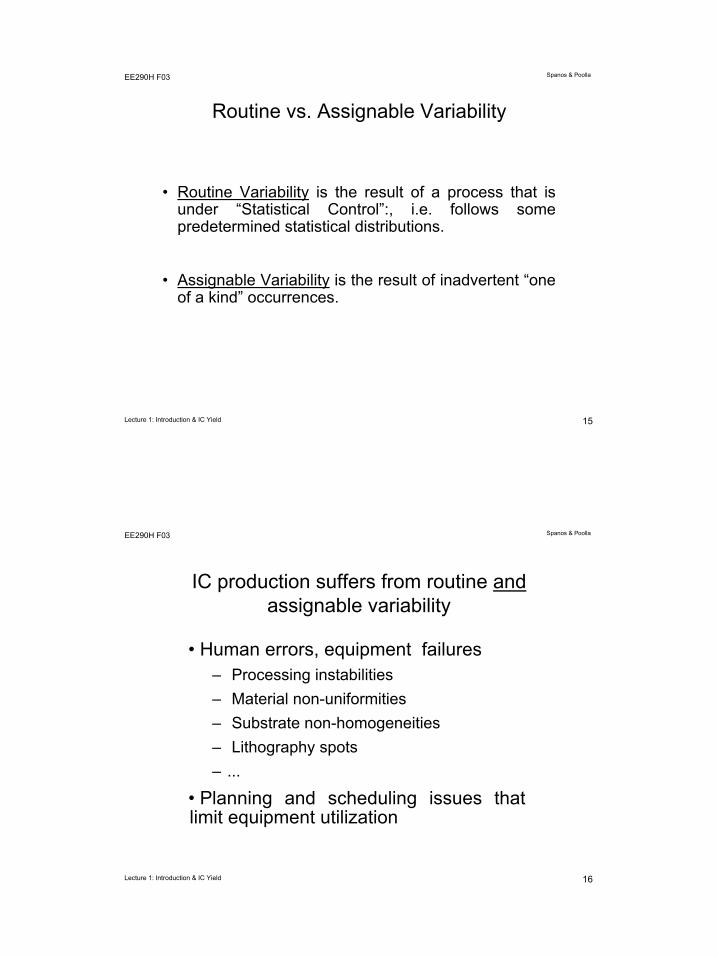
Routine vs. Assignable Variability
• Routine Variability is the result of a process that is under “Statistical Control”:, i.e. follows some predetermined statistical distributions.
• Assignable Variability is the result of inadvertent “one of a kind” occurrences.
16Lecture 1: Introduction & IC Yield
Spanos & PoollaEE290H F03
IC production suffers from routine andassignable variability
• Human errors, equipment failures– Processing instabilities– Material non-uniformities– Substrate non-homogeneities– Lithography spots– ...
• Planning and scheduling issues that limit equipment utilization

17Lecture 1: Introduction & IC Yield
Spanos & PoollaEE290H F03
Process Variability Causes Deformations
• Geometrical • Electrical° Lateral ° Global° Vertical ° Local° Spot defects
Deformations have deterministic andrandom components, are global and/orlocal, can be independent or can interact.
18Lecture 1: Introduction & IC Yield
Spanos & PoollaEE290H F03
Deformations of Ideal Design
Atlas of IC Technologies - An Introduction to VLSI Processes, W. Maly, The Benjamin/Cummins Publishing Company, Inc, 1987
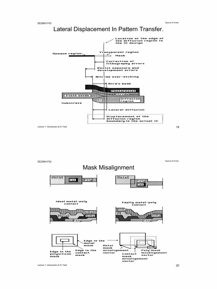
19Lecture 1: Introduction & IC Yield
Spanos & PoollaEE290H F03
Lateral Displacement In Pattern Transfer.
20Lecture 1: Introduction & IC Yield
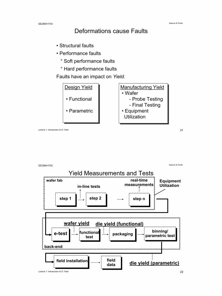
Spanos & PoollaEE290H F03
Mask Misalignment
21Lecture 1: Introduction & IC Yield
Spanos & PoollaEE290H F03
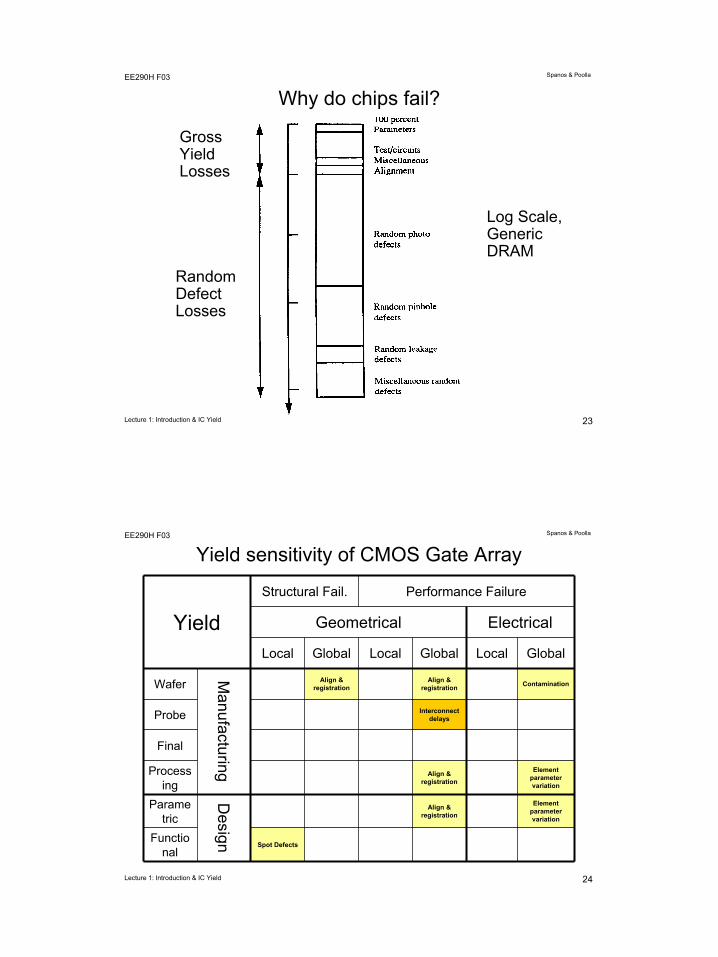
Deformations cause Faults
Design Yield
• Functional
• Parametric
Design Yield
• Functional
• Parametric
Manufacturing Yield• Wafer
- Probe Testing- Final Testing
• Equipment Utilization
Manufacturing Yield• Wafer
- Probe Testing- Final Testing
• Equipment Utilization
• Structural faults• Performance faults
° Soft performance faults° Hard performance faults
Faults have an impact on Yield.
22Lecture 1: Introduction & IC Yield
Spanos & PoollaEE290H F03
Yield Measurements and Tests
step 1 step 2 step n
e-test packagingfunctionaltest
binning/parametric test
field installation
in-line testsreal-time
measurements
fielddata
wafer fab
wafer yield die yield (functional)
die yield (parametric)
back-end
EquipmentUtilization
23Lecture 1: Introduction & IC Yield
Spanos & PoollaEE290H F03
Why do chips fail?
GrossYieldLosses
Random DefectLosses
Log Scale,GenericDRAM
24Lecture 1: Introduction & IC Yield
Spanos & PoollaEE290H F03
Yield sensitivity of CMOS Gate Array
Spot DefectsFunctio
nal
Element parameter variation
Align & registration
Design
Parametric
Element parameter variation
Align & registration
Processing
Final
Interconnect delaysProbe
ContaminationAlign & registration
Align & registration
Manufacturing
Wafer
GlobalLocalGlobalLocalGlobalLocal
ElectricalGeometrical
Performance FailureStructural Fail.
Yield
25Lecture 1: Introduction & IC Yield
Spanos & PoollaEE290H F03
Yield Sensitivity of Large DRAM
Spot DefectsFunctio
nal
Element parameter variation
Align & registration
Align & registration
Design
Parametric
Element parameter variation
Align & registration
Align & registration
Processing
Interconnect delaysSpot Defects Final
Interconnect delaysSpot DefectsProbe
ContaminationEtchingWafer Deform
Manufacturing
Wafer
GlobalLocalGlobalLocalGlobalLocal
ElectricalGeometrical
Performance FailureStructural Fail.
Yield
26Lecture 1: Introduction & IC Yield
Spanos & PoollaEE290H F03
Yield Sensitivity of Bipolar Op Amp
Spikes, pipes, etc
Align & registration
Spikes, pipes, etc
Functional
Element parameter variation
Design
Parametric
Bar tr. parameters
Spikes, pipes, etc
Align & registration
Spikes, pipes, etc
Processing
Final
Bar tr. parameters
Spikes, pipes, etc.
Align & registration
Spikes, pipes, etc.Probe
DIP Effect
Manufacturing
Wafer
GlobalLocalGlobalLocalGlobalLocal
ElectricalGeometrical
Performance FailureStructural Fail.
Yield

27Lecture 1: Introduction & IC Yield
Spanos & PoollaEE290H F03
What limits Functional Yield?
• Gross Misalignments• Particles• Mask Defects• In general, the above are considered random
events, and their assumed distribution plays a profound role in decisions having to do with:– Metrology (how often and what we measure)– Modeling (how one can predict the occurrence of these
events)– Simulation (calculating how a specific IC layout will do)– Design rules/styles to “immunize” the IC to defects
28Lecture 1: Introduction & IC Yield
Spanos & PoollaEE290H F03
Particles vs. Defects
• Particles come from outside the device structure
• Defects are created within the device structure
Aluminum spiking
Interconnect patterning
etc.

29Lecture 1: Introduction & IC Yield
Spanos & PoollaEE290H F03
Particles
Picture 26, pp 185 Yield Book
30Lecture 1: Introduction & IC Yield
Spanos & PoollaEE290H F03
Where do particles come from?
• People
• Material Handling
• Processing chambers
31Lecture 1: Introduction & IC Yield
Spanos & PoollaEE290H F03
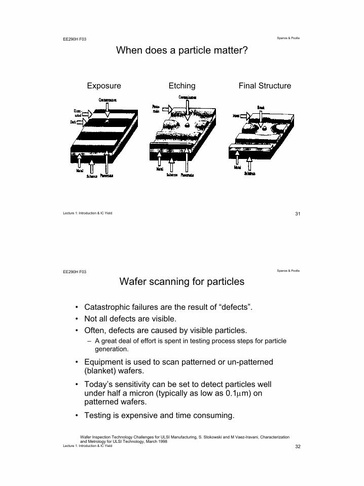
When does a particle matter?
Exposure Etching Final Structure
32Lecture 1: Introduction & IC Yield
Spanos & PoollaEE290H F03
Wafer scanning for particles
• Catastrophic failures are the result of “defects”.• Not all defects are visible.• Often, defects are caused by visible particles.
– A great deal of effort is spent in testing process steps for particle generation.
• Equipment is used to scan patterned or un-patterned (blanket) wafers.
• Today’s sensitivity can be set to detect particles well under half a micron (typically as low as 0.1µm) on patterned wafers.
• Testing is expensive and time consuming.
Wafer Inspection Technology Challenges for ULSI Manufacturing, S. Stokowski and M Vaez-Iravani, Characterization and Metrology for ULSI Technology, March 1998
33Lecture 1: Introduction & IC Yield
Spanos & PoollaEE290H F03
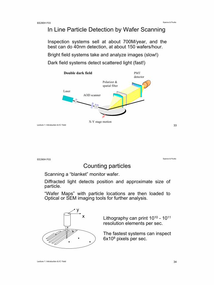
In Line Particle Detection by Wafer Scanning
Inspection systems sell at about 700M/year, and the best can do 40nm detection, at about 150 wafers/hour.
Bright field systems take and analyze images (slow!)
Dark field systems detect scattered light (fast!)
AOD scanner
PMTdetector
Polarizer &spatial filter
Laser
X-Y stage motion
Double dark field
34Lecture 1: Introduction & IC Yield
Spanos & PoollaEE290H F03
Counting particlesScanning a “blanket” monitor wafer. Diffracted light detects position and approximate size of particle.“Wafer Maps” with particle locations are then loaded to Optical or SEM imaging tools for further analysis.
xy
Lithography can print 1010 - 1011
resolution elements per sec.
The fastest systems can inspect 6x108 pixels per sec.
35Lecture 1: Introduction & IC Yield
Spanos & PoollaEE290H F03
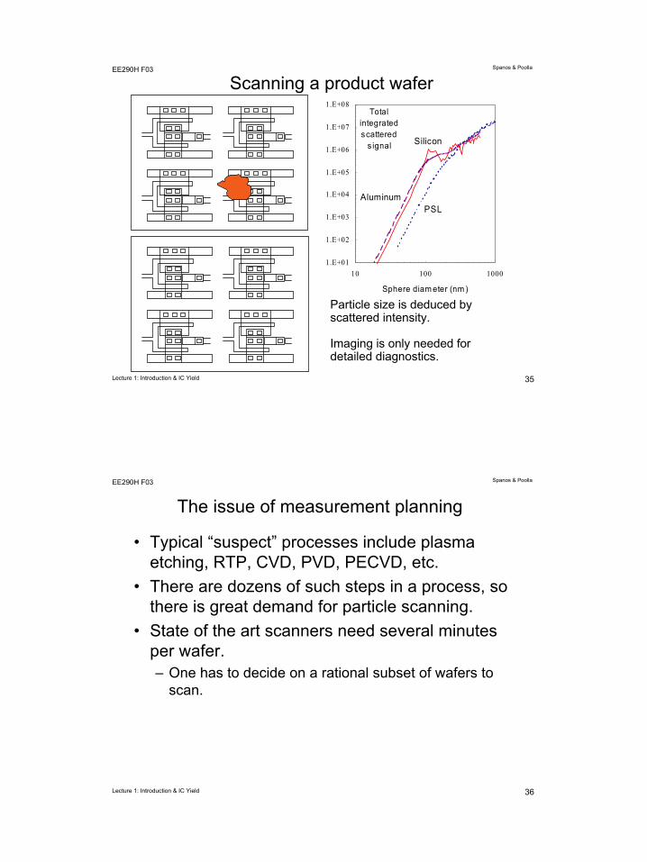
Scanning a product wafer
1.E+01
1.E+02
1.E+03
1.E+04
1.E+05
1.E+06
1.E+07
1.E+08
10 100 1000
Sphere diam eter (nm )
Total integrated scattered
s ignal
PSL
Silicon
Aluminum
Particle size is deduced by scattered intensity.
Imaging is only needed for detailed diagnostics.
36Lecture 1: Introduction & IC Yield
Spanos & PoollaEE290H F03
The issue of measurement planning
• Typical “suspect” processes include plasma etching, RTP, CVD, PVD, PECVD, etc.
• There are dozens of such steps in a process, so there is great demand for particle scanning.
• State of the art scanners need several minutes per wafer.– One has to decide on a rational subset of wafers to
scan.

37Lecture 1: Introduction & IC Yield
Spanos & PoollaEE290H F03
The Resource Allocation Problem
Since wafer scanning is expensive, we must create an “optimum” plan for testing a meaningful allocation.
Plans can be adaptive, so that dirty wafers receive more scrutiny.
38Lecture 1: Introduction & IC Yield
Spanos & PoollaEE290H F03
Acceptance Sampling
Acceptance sampling is not a substitute for process control or good DFM practices.
Acceptance sampling is a general collection of methods designed to inspect the finished product.
How many wafers do we sample per lot? How many points we measure per wafer?
39Lecture 1: Introduction & IC Yield
Spanos & PoollaEE290H F03
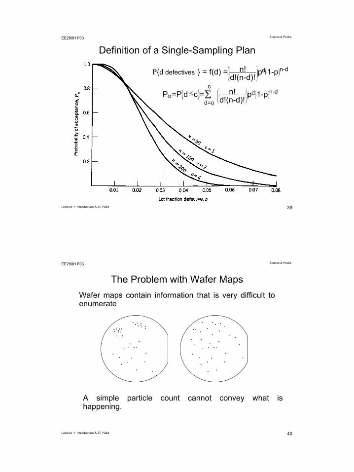
Definition of a Single-Sampling Plan
P{d defectives } = f(d) = n!d!(n-d)!
pd 1-p n-d
Pα=P d ≤c = n!d!(n-d)!
pd 1-p n-dΣd=o
c
40Lecture 1: Introduction & IC Yield
Spanos & PoollaEE290H F03
The Problem with Wafer MapsWafer maps contain information that is very difficult to enumerate
A simple particle count cannot convey what is happening.
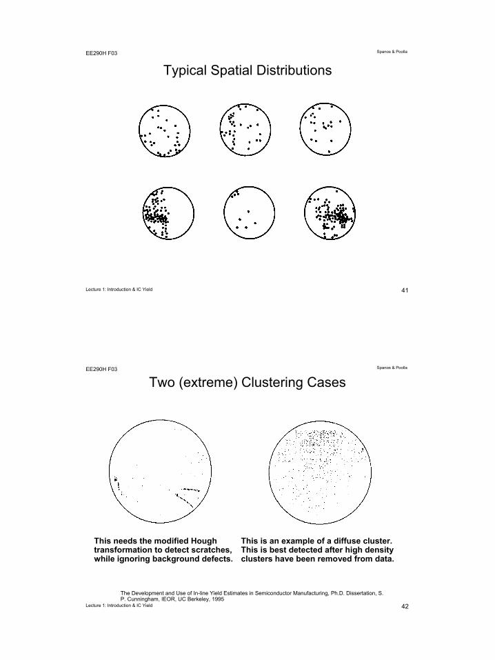
41Lecture 1: Introduction & IC Yield
Spanos & PoollaEE290H F03
Typical Spatial Distributions
42Lecture 1: Introduction & IC Yield
Spanos & PoollaEE290H F03
Two (extreme) Clustering Cases
This needs the modified Houghtransformation to detect scratches, while ignoring background defects.
This is an example of a diffuse cluster.This is best detected after high density clusters have been removed from data.
The Development and Use of In-line Yield Estimates in Semiconductor Manufacturing, Ph.D. Dissertation, S. P. Cunningham, IEOR, UC Berkeley, 1995
43Lecture 1: Introduction & IC Yield
Spanos & PoollaEE290H F03
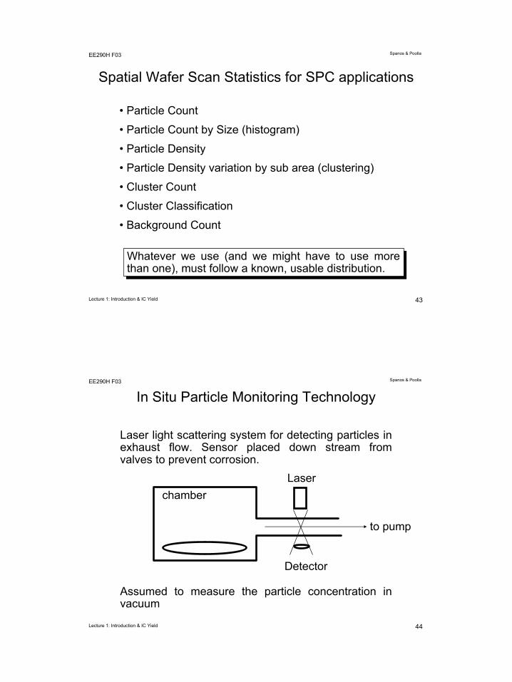
Spatial Wafer Scan Statistics for SPC applications
• Particle Count
• Particle Count by Size (histogram)
• Particle Density
• Particle Density variation by sub area (clustering)
• Cluster Count
• Cluster Classification
• Background Count
Whatever we use (and we might have to use more than one), must follow a known, usable distribution.Whatever we use (and we might have to use more than one), must follow a known, usable distribution.
44Lecture 1: Introduction & IC Yield
Spanos & PoollaEE290H F03
In Situ Particle Monitoring Technology
Laser light scattering system for detecting particles in exhaust flow. Sensor placed down stream from valves to prevent corrosion.
chamberLaser
Detector
to pump
Assumed to measure the particle concentration in vacuum
45Lecture 1: Introduction & IC Yield
Spanos & PoollaEE290H F03
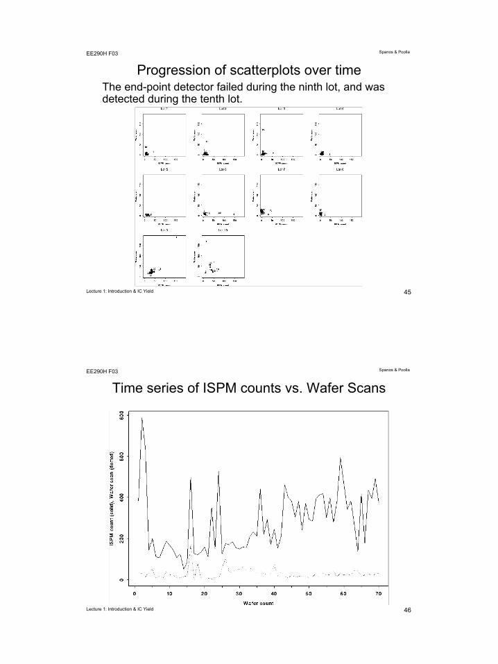
Progression of scatterplots over timeThe end-point detector failed during the ninth lot, and was detected during the tenth lot.
46Lecture 1: Introduction & IC Yield
Spanos & PoollaEE290H F03
Time series of ISPM counts vs. Wafer Scans

47Lecture 1: Introduction & IC Yield
Spanos & PoollaEE290H F03
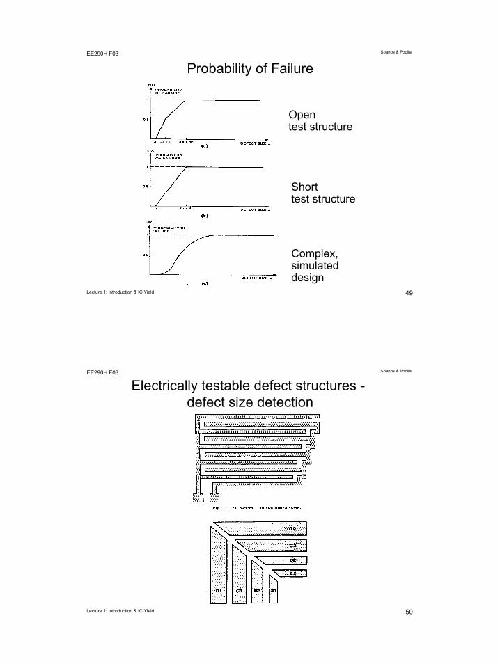
Drawing inferences from electrical test patterns
• Often one resorts to much faster (but less accurate) testing of electrical structures designed for particle detection.
• These can only be used on conductive layers, at the end of a process.
• Can detect shorts, opens in one layer, or shorts between layers.
• One must make assumptions about defect size and density in interpreting these results.
48Lecture 1: Introduction & IC Yield
Spanos & PoollaEE290H F03
Electrically testable defect structure -Short/Open detection
49Lecture 1: Introduction & IC Yield
Spanos & PoollaEE290H F03
Probability of Failure
Opentest structure
Shorttest structure
Complex,simulateddesign
50Lecture 1: Introduction & IC Yield
Spanos & PoollaEE290H F03
Electrically testable defect structures -defect size detection
51Lecture 1: Introduction & IC Yield
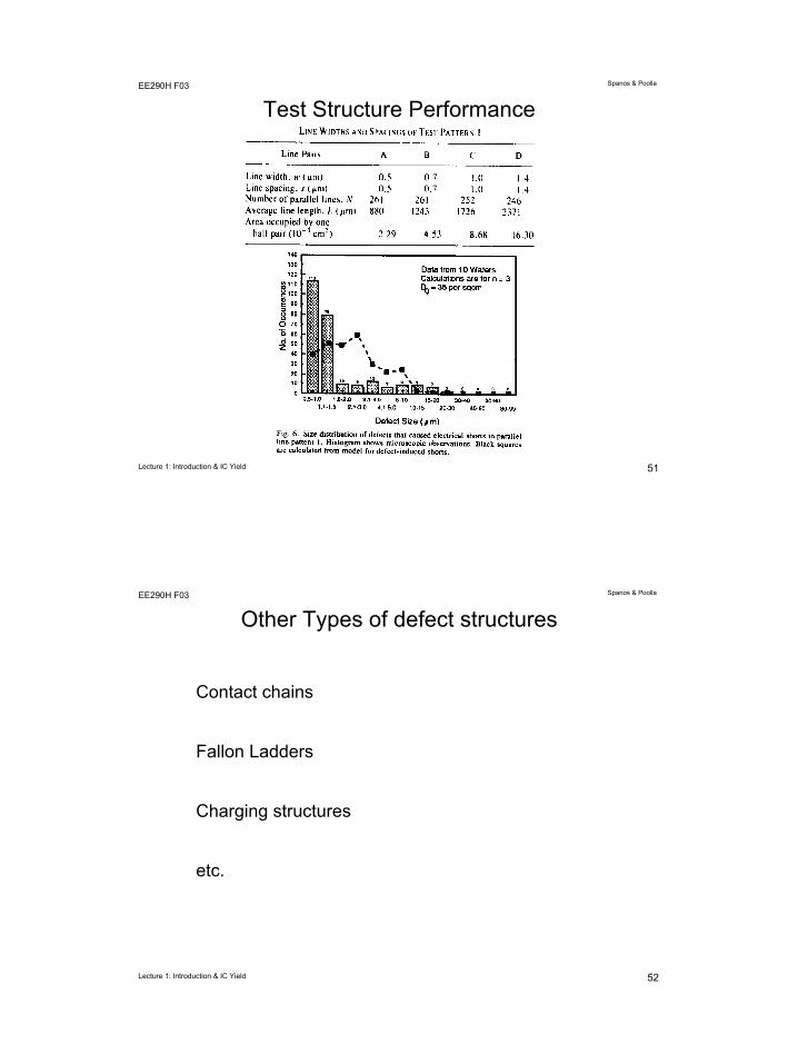
Spanos & PoollaEE290H F03
Test Structure Performance
52Lecture 1: Introduction & IC Yield
Spanos & PoollaEE290H F03
Other Types of defect structures
Contact chains
Fallon Ladders
Charging structures
etc.
53Lecture 1: Introduction & IC Yield
Spanos & PoollaEE290H F03
Use of in-line yield metrology
• Wafer screening
• Machine maintenance
• Yield learning
• Modeling (next time!)
• Design fault tolerant circuits
54Lecture 1: Introduction & IC Yield
Spanos & PoollaEE290H F03
Functional Yield Modeling
Early Yield Models
Murhpy’s
Modified Poisson
Negative Binomial
Component Models
55Lecture 1: Introduction & IC Yield
Spanos & PoollaEE290H F03
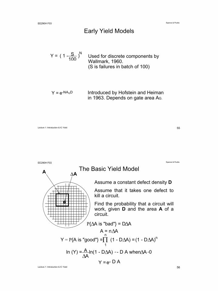
Early Yield Models
Y = ( 1 - S100
)N
Y = e-NAGD
Used for discrete components byWallmark, 1960.(S is failures in batch of 100)
Introduced by Hofstein and Heimanin 1963. Depends on gate area AG.
56Lecture 1: Introduction & IC Yield
Spanos & PoollaEE290H F03
The Basic Yield Model
Assume a constant defect density DAssume that it takes one defect to kill a circuit.
Find the probability that a circuit will work, given D and the area A of a circuit.
A ∆A
P{∆A is "bad"} = D ∆AA = n ∆A
Y = P{A is "good"} = (1 - D ∆A) = (1 - D ∆A)nΠ1
n
ln (Y) = A∆A
ln(1 - D ∆A) → - D A when ∆A→0
Y = e- D A
57Lecture 1: Introduction & IC Yield
Spanos & PoollaEE290H F03
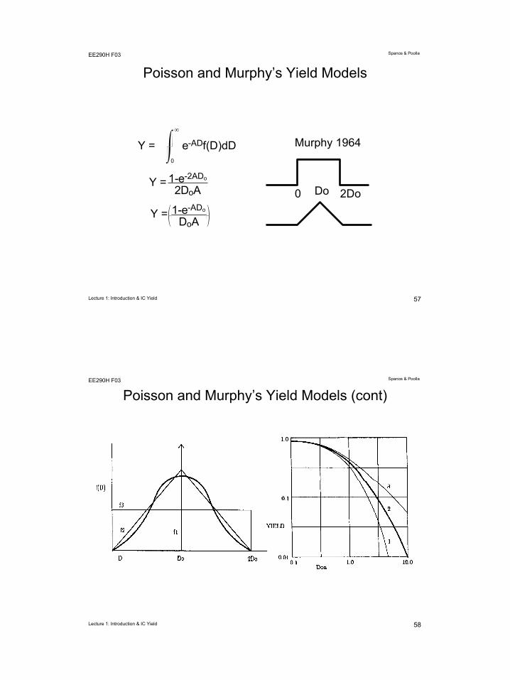
Poisson and Murphy’s Yield Models
Y = e-AD
0
∞
f(D)dD
Y = 1-e-2ADo
2DoA
Y = 1-e-ADo
DoA
0 Do 2Do
Murphy 1964
58Lecture 1: Introduction & IC Yield
Spanos & PoollaEE290H F03
Poisson and Murphy’s Yield Models (cont)
59Lecture 1: Introduction & IC Yield
Spanos & PoollaEE290H F03
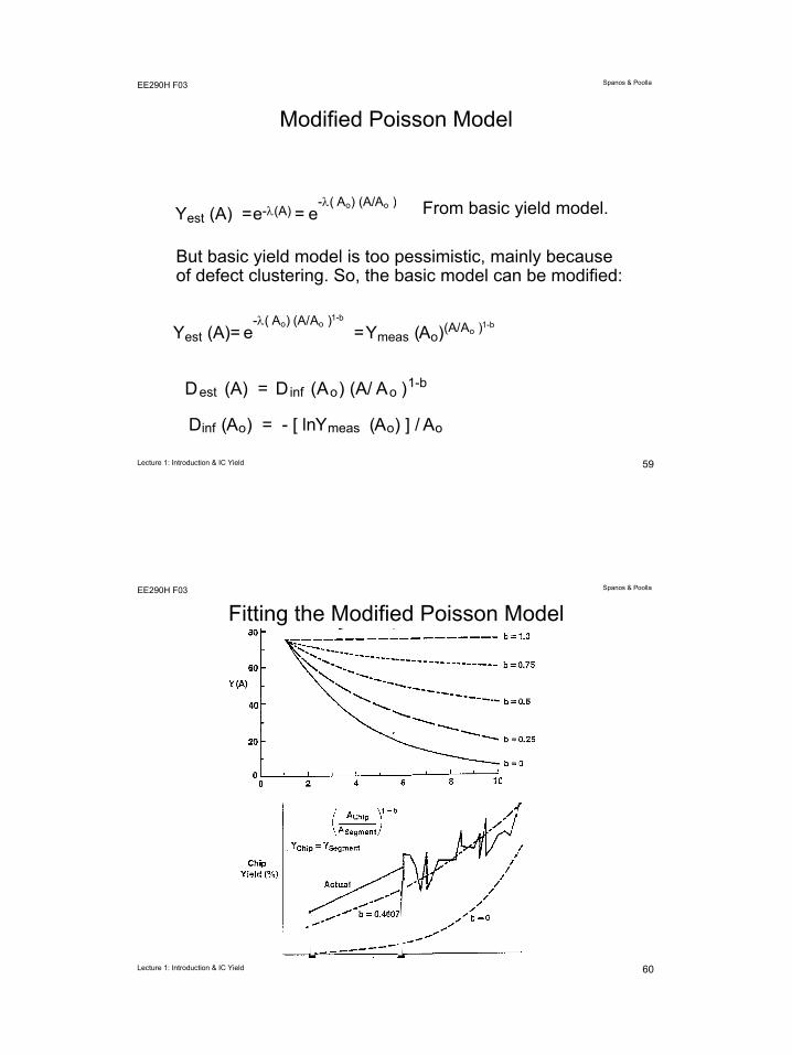
Modified Poisson Model
Yest (A) = e-λ(A) = e-λ( Ao) (A/Ao )
Yest (A)= e-λ( Ao) (A/Ao )1-b
= Ymeas (Ao)(A/Ao )1-b
From basic yield model.
But basic yield model is too pessimistic, mainly becauseof defect clustering. So, the basic model can be modified:
Dest (A) = Dinf (Ao) (A/ Ao )1-b
Dinf (Ao) = - [ lnYmeas (Ao) ] / Ao
60Lecture 1: Introduction & IC Yield
Spanos & PoollaEE290H F03
Fitting the Modified Poisson Model
61Lecture 1: Introduction & IC Yield
Spanos & PoollaEE290H F03
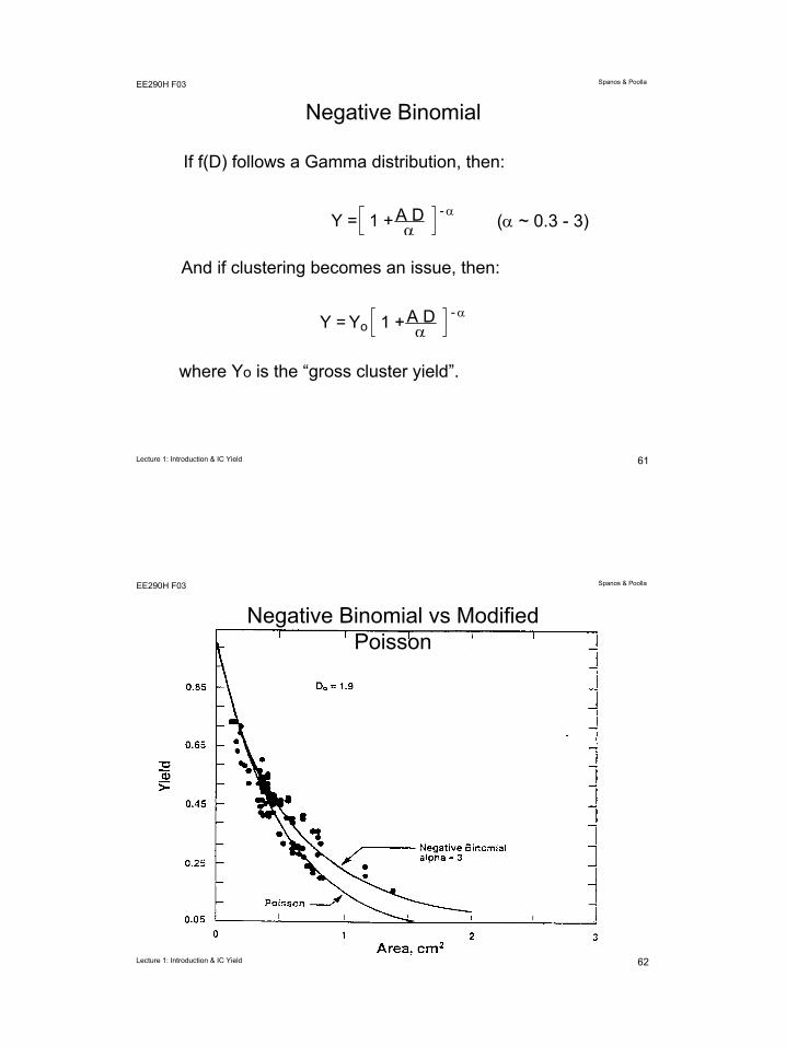
Negative Binomial
If f(D) follows a Gamma distribution, then:
Y = 1 + A Dα - α
And if clustering becomes an issue, then:
Y = Yo 1 + A Dα - α
where Yo is the “gross cluster yield”.
(α ~ 0.3 - 3)
62Lecture 1: Introduction & IC Yield
Spanos & PoollaEE290H F03
Negative Binomial vs Modified Poisson
63Lecture 1: Introduction & IC Yield
Spanos & PoollaEE290H F03
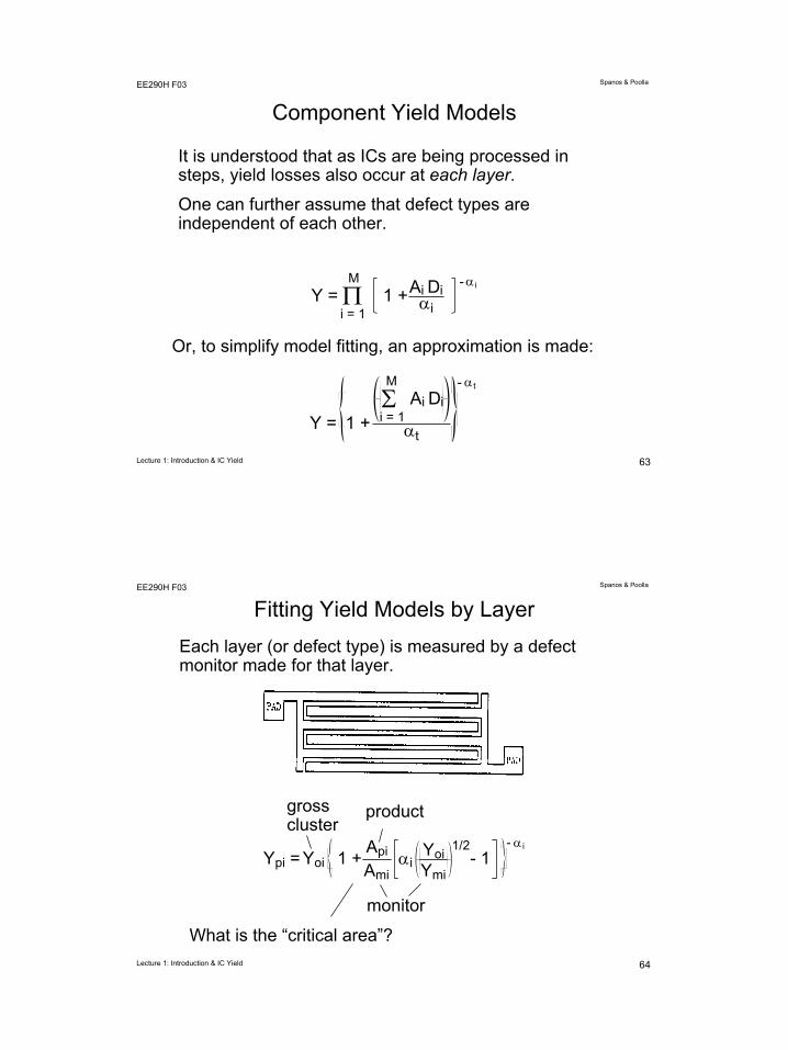
Component Yield Models
It is understood that as ICs are being processed in steps, yield losses also occur at each layer.
One can further assume that defect types are independent of each other.
Y = 1 + Ai Diαi
-αi
Πi = 1
M
Or, to simplify model fitting, an approximation is made:
Y = 1 + Ai DiΣ
i = 1
M
αt
- αt
64Lecture 1: Introduction & IC Yield
Spanos & PoollaEE290H F03
Fitting Yield Models by LayerEach layer (or defect type) is measured by a defect monitor made for that layer.
Ypi = Yoi 1 + ApiAmi
αi YoiYmi
1/2- 1
- α i
grosscluster
product
monitor
What is the “critical area”?
65Lecture 1: Introduction & IC Yield
Spanos & PoollaEE290H F03
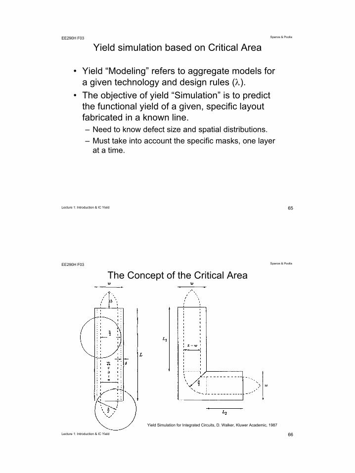
Yield simulation based on Critical Area
• Yield “Modeling” refers to aggregate models for a given technology and design rules (λ).
• The objective of yield “Simulation” is to predict the functional yield of a given, specific layout fabricated in a known line.– Need to know defect size and spatial distributions.– Must take into account the specific masks, one layer
at a time.
66Lecture 1: Introduction & IC Yield
Spanos & PoollaEE290H F03
The Concept of the Critical Area
Yield Simulation for Integrated Circuits, D. Walker, Kluwer Academic, 1987

67Lecture 1: Introduction & IC Yield
Spanos & PoollaEE290H F03
What do we need to know about particles
• Spatial distribution
• Size distribution
• Interaction of above with layout of circuit
68Lecture 1: Introduction & IC Yield
Spanos & PoollaEE290H F03
Typical Defect Size Distribution
69Lecture 1: Introduction & IC Yield
Spanos & PoollaEE290H F03
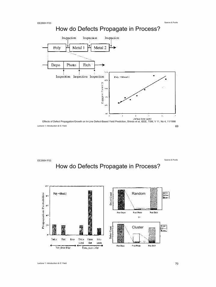
How do Defects Propagate in Process?
Effects of Defect Propagation/Growth on In-Line Defect-Based Yield Prediction, Shindo et al, IEEE, TSM, V 11, No 4, 11/1998
70Lecture 1: Introduction & IC Yield
Spanos & PoollaEE290H F03
How do Defects Propagate in Process?
Random
Cluster
71Lecture 1: Introduction & IC Yield
Spanos & PoollaEE290H F03
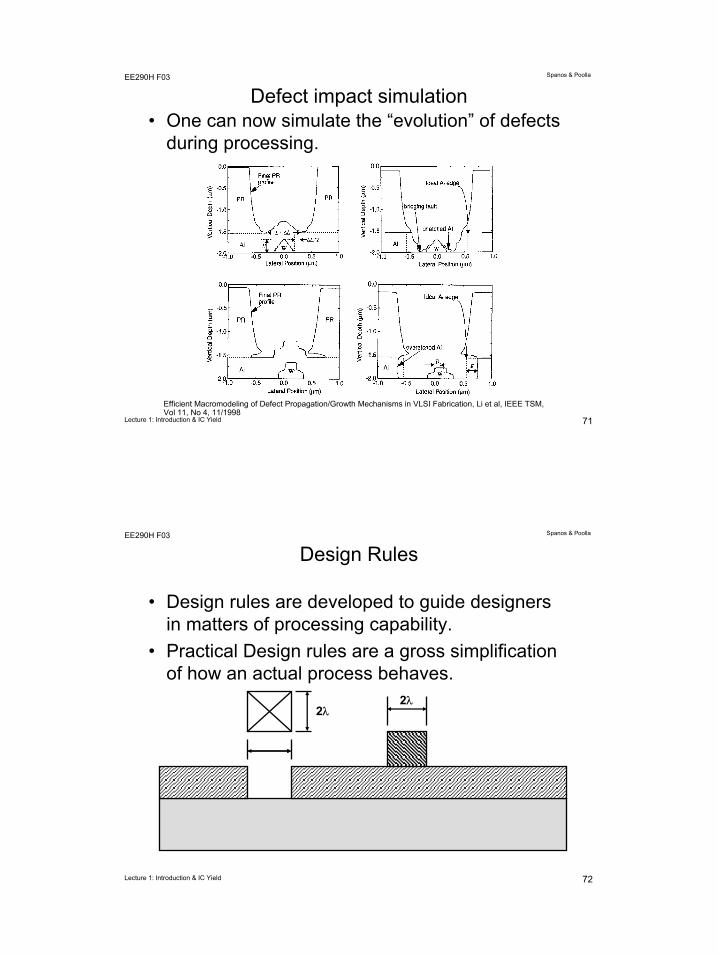
Defect impact simulation• One can now simulate the “evolution” of defects
during processing.
Efficient Macromodeling of Defect Propagation/Growth Mechanisms in VLSI Fabrication, Li et al, IEEE TSM, Vol 11, No 4, 11/1998
72Lecture 1: Introduction & IC Yield
Spanos & PoollaEE290H F03
Design Rules
• Design rules are developed to guide designers in matters of processing capability.
• Practical Design rules are a gross simplification of how an actual process behaves.
2λ2λ
73Lecture 1: Introduction & IC Yield
Spanos & PoollaEE290H F03
Design Rules (cont)
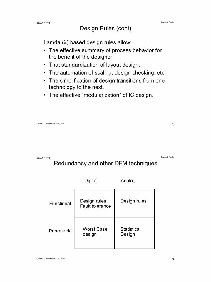
Lamda (λ) based design rules allow:• The effective summary of process behavior for
the benefit of the designer.• That standardization of layout design.• The automation of scaling, design checking, etc.• The simplification of design transitions from one
technology to the next.• The effective “modularization” of IC design.
74Lecture 1: Introduction & IC Yield
Spanos & PoollaEE290H F03
Redundancy and other DFM techniques
Design rulesFault tolerance
Design rules
Worst Case design
Statistical Design
Digital Analog
Functional
Parametric
75Lecture 1: Introduction & IC Yield
Spanos & PoollaEE290H F03
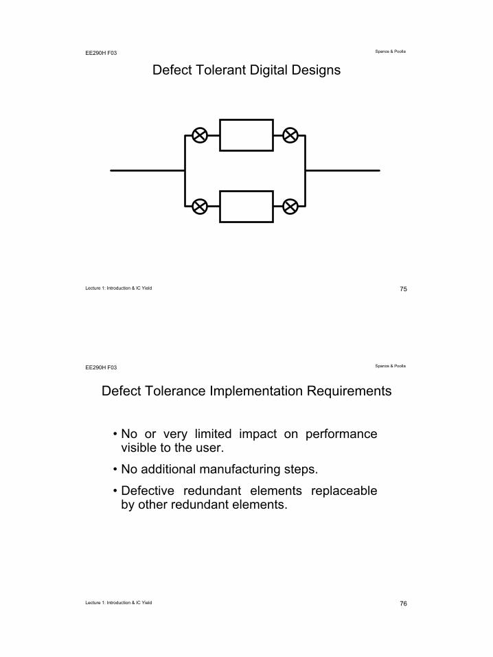
Defect Tolerant Digital Designs
76Lecture 1: Introduction & IC Yield
Spanos & PoollaEE290H F03
Defect Tolerance Implementation Requirements
• No or very limited impact on performance visible to the user.
• No additional manufacturing steps.
• Defective redundant elements replaceable by other redundant elements.
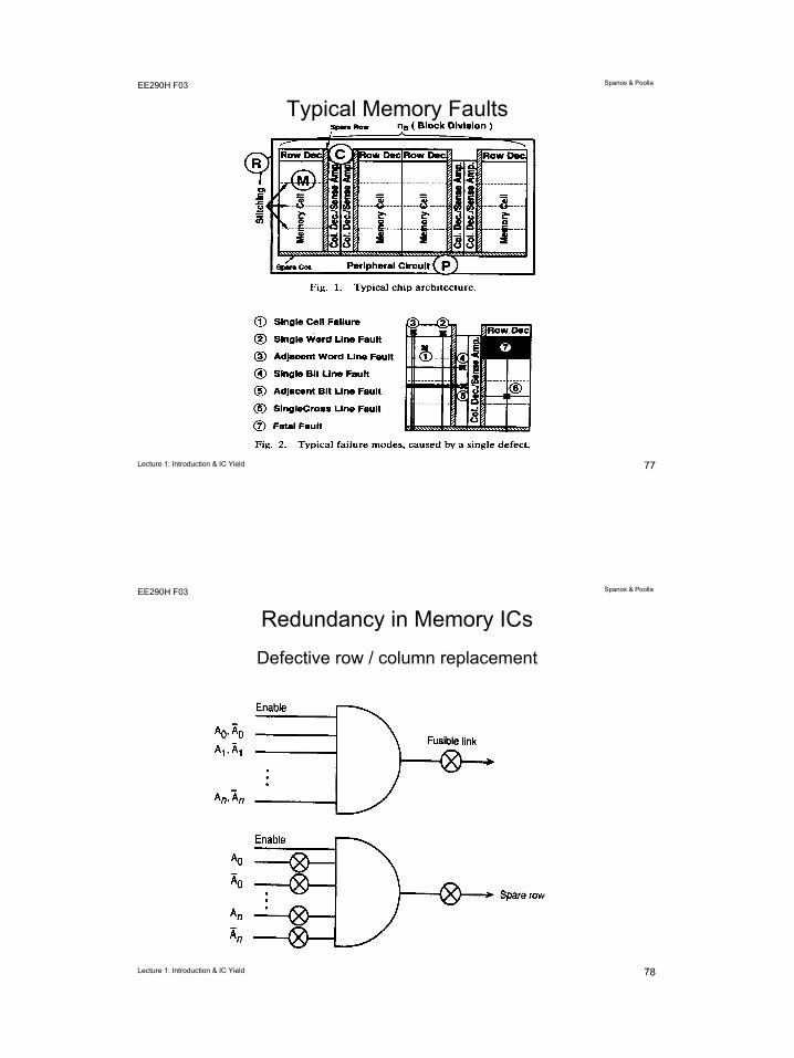
77Lecture 1: Introduction & IC Yield
Spanos & PoollaEE290H F03
Typical Memory Faults
78Lecture 1: Introduction & IC Yield
Spanos & PoollaEE290H F03
Redundancy in Memory ICs
Defective row / column replacement

79Lecture 1: Introduction & IC Yield
Spanos & PoollaEE290H F03
The problem with fuse links
• Electrical fuses are not very reliable.• Laser trimming is expensive.• Best techniques involve non-volatile memory
programming.
80Lecture 1: Introduction & IC Yield
Spanos & PoollaEE290H F03
Error Correcting Code Example
0 63...
Data Bits Parity Bits
Parity allows correction of 16 kilobit failures out of 1 megabit.
Consecutive bits in a word are stored at least 15 cells apart
i i+1
0 6
81Lecture 1: Introduction & IC Yield
Spanos & PoollaEE290H F03
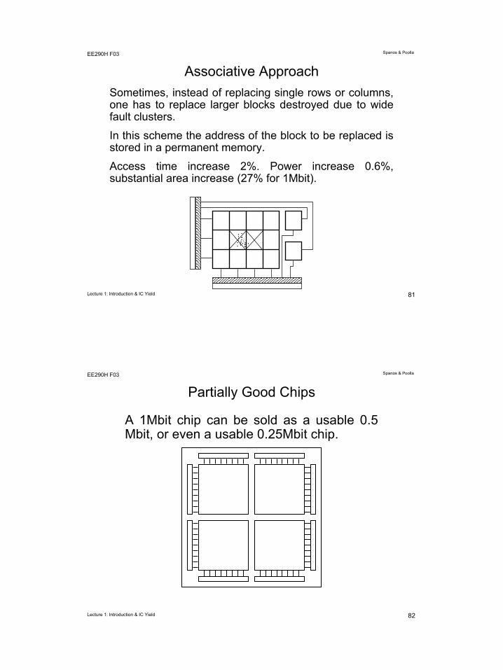
Associative ApproachSometimes, instead of replacing single rows or columns, one has to replace larger blocks destroyed due to wide fault clusters.
In this scheme the address of the block to be replaced is stored in a permanent memory.
Access time increase 2%. Power increase 0.6%, substantial area increase (27% for 1Mbit).
82Lecture 1: Introduction & IC Yield
Spanos & PoollaEE290H F03
Partially Good Chips
A 1Mbit chip can be sold as a usable 0.5 Mbit, or even a usable 0.25Mbit chip.
83Lecture 1: Introduction & IC Yield
Spanos & PoollaEE290H F03
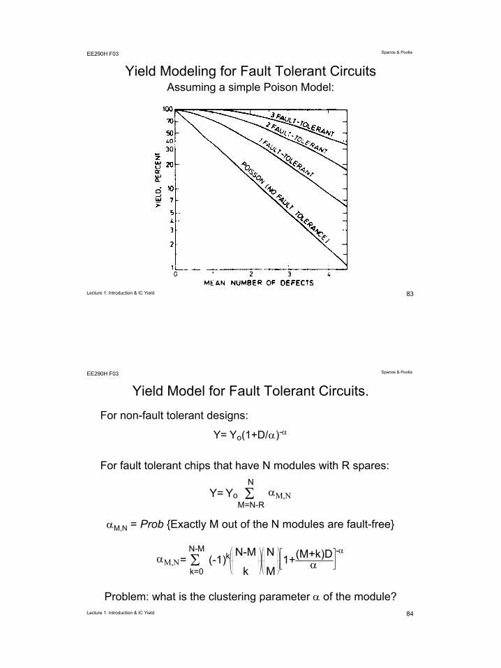
Yield Modeling for Fault Tolerant CircuitsAssuming a simple Poison Model:
84Lecture 1: Introduction & IC Yield
Spanos & PoollaEE290H F03
Yield Model for Fault Tolerant Circuits.
Y= Yo(1+D/α)-α
αM,N = Prob {Exactly M out of the N modules are fault-free}
Y= Yo ΣM=N-R
NαM,N
Problem: what is the clustering parameter α of the module?
αM,N= Σk=0
N-M(-1)k
N-M
k
N
M1+(M+k)D
α-α
For non-fault tolerant designs:
For fault tolerant chips that have N modules with R spares:
85Lecture 1: Introduction & IC Yield
Spanos & PoollaEE290H F03
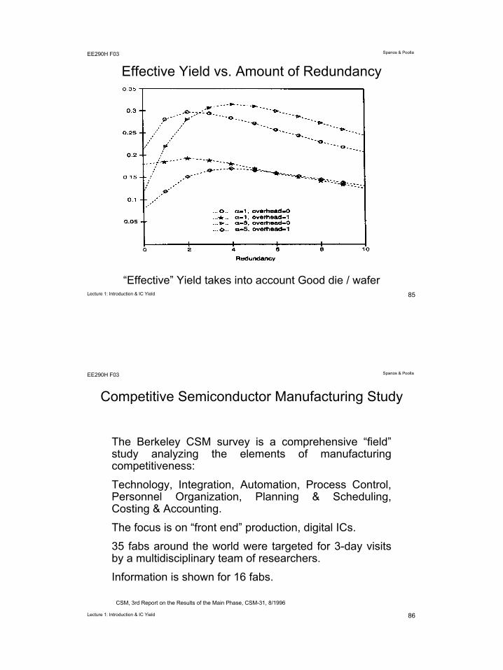
Effective Yield vs. Amount of Redundancy
“Effective” Yield takes into account Good die / wafer
86Lecture 1: Introduction & IC Yield
Spanos & PoollaEE290H F03
Competitive Semiconductor Manufacturing Study
The Berkeley CSM survey is a comprehensive “field” study analyzing the elements of manufacturing competitiveness:
Technology, Integration, Automation, Process Control, Personnel Organization, Planning & Scheduling, Costing & Accounting.
The focus is on “front end” production, digital ICs.
35 fabs around the world were targeted for 3-day visits by a multidisciplinary team of researchers.
Information is shown for 16 fabs.
CSM, 3rd Report on the Results of the Main Phase, CSM-31, 8/1996
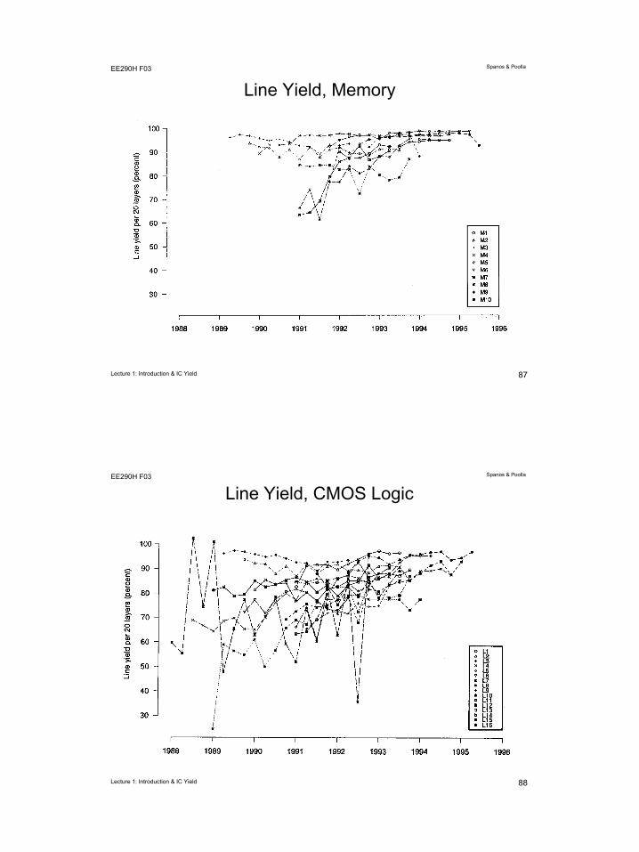
87Lecture 1: Introduction & IC Yield
Spanos & PoollaEE290H F03
Line Yield, Memory
88Lecture 1: Introduction & IC Yield
Spanos & PoollaEE290H F03
Line Yield, CMOS Logic
89Lecture 1: Introduction & IC Yield
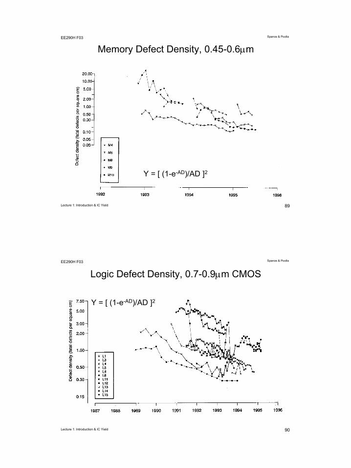
Spanos & PoollaEE290H F03
Memory Defect Density, 0.45-0.6µm
Y = [ (1-e-AD)/AD ]2
90Lecture 1: Introduction & IC Yield
Spanos & PoollaEE290H F03
Logic Defect Density, 0.7-0.9µm CMOS
Y = [ (1-e-AD)/AD ]2
91Lecture 1: Introduction & IC Yield
Spanos & PoollaEE290H F03
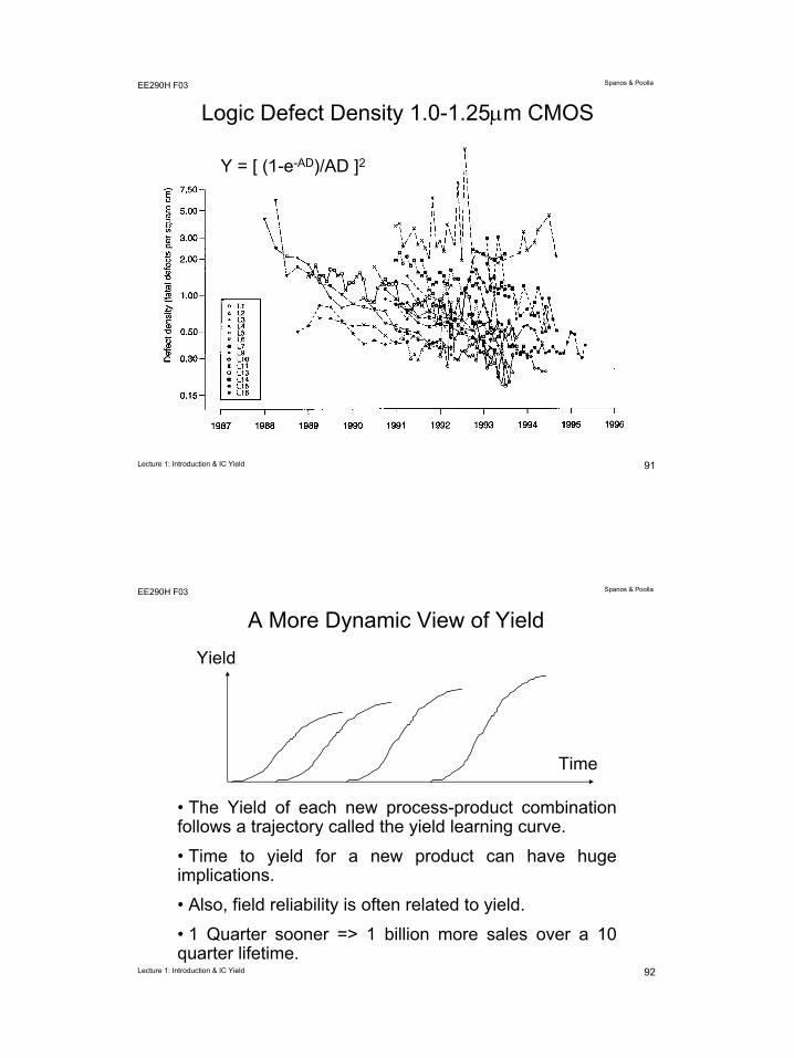
Logic Defect Density 1.0-1.25µm CMOS
Y = [ (1-e-AD)/AD ]2
92Lecture 1: Introduction & IC Yield
Spanos & PoollaEE290H F03
A More Dynamic View of Yield
• The Yield of each new process-product combination follows a trajectory called the yield learning curve.
• Time to yield for a new product can have huge implications.
• Also, field reliability is often related to yield.
• 1 Quarter sooner => 1 billion more sales over a 10 quarter lifetime.
Time
Yield
93Lecture 1: Introduction & IC Yield
Spanos & PoollaEE290H F03
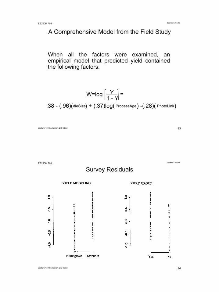
A Comprehensive Model from the Field Study
When all the factors were examined, an empirical model that predicted yield contained the following factors:
W=log Y1 - Y
=
.38 - (.96)(dieSize) + (.37)log( ProcessAge) -(.28)( PhotoLink)
94Lecture 1: Introduction & IC Yield
Spanos & PoollaEE290H F03
Survey Residuals
95Lecture 1: Introduction & IC Yield
Spanos & PoollaEE290H F03
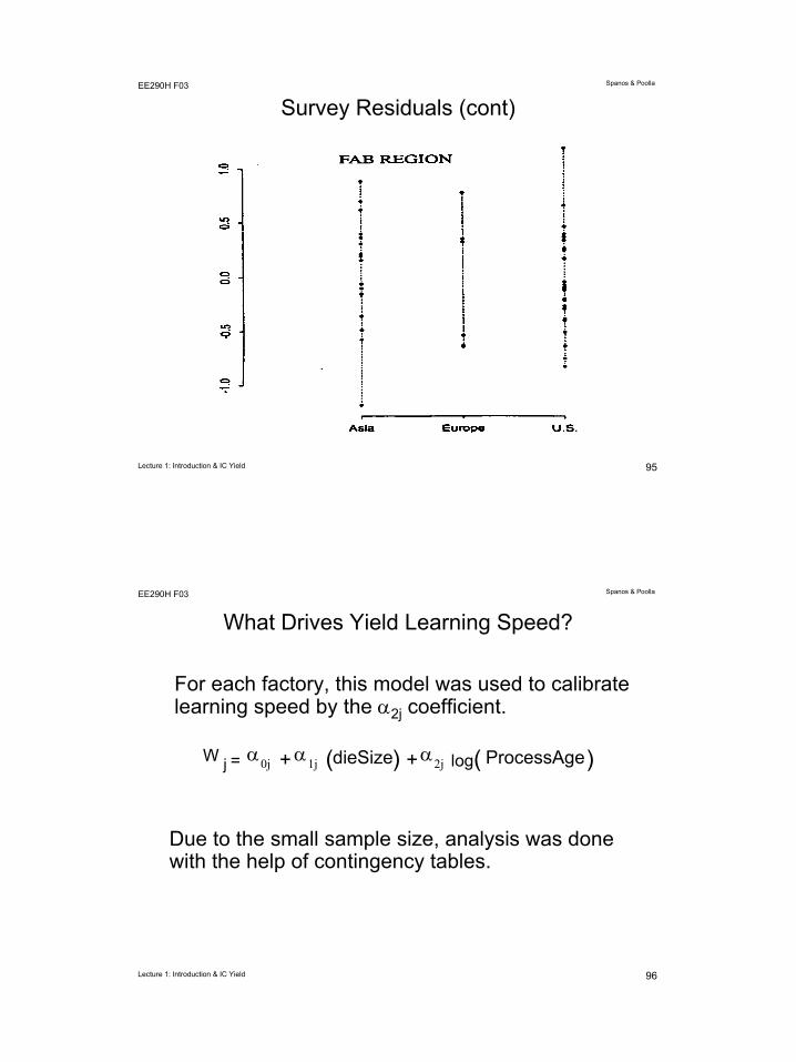
Survey Residuals (cont)
96Lecture 1: Introduction & IC Yield
Spanos & PoollaEE290H F03
What Drives Yield Learning Speed?
W j = α0j +α1j (dieSize) +α2j log( ProcessAge)
For each factory, this model was used to calibrate learning speed by the α2j coefficient.
Due to the small sample size, analysis was done with the help of contingency tables.

97Lecture 1: Introduction & IC Yield
Spanos & PoollaEE290H F03
What Drives Yield Learning Speed? (cont)
98Lecture 1: Introduction & IC Yield
Spanos & PoollaEE290H F03
In SummaryYield modeling, measurement and control is vital in semiconductor manufacturing.
“Process Control” has interesting technical, as well as cultural aspects.
Yield learning is driven by competition and made even because of an ever improving equipment base.
Future advances will further decrease cycle time, increase wafer and die yield, and give more uniform performances for current geometries.
It will be a serious challenge to bring these improvements to the factory of 2010 with 0.03µm geometries and >>12 inch wafers.
Next frontier for yield improvement: Parametric Considerations and Equipment Utilization!


![Cyber Security for Smart Grid Devices - TCIPG · Applications Symposium2008 ] Optimal Contracts for Wind Power Producers in Electricity Markets (Poolla) [CDC 2010] Renewable integration](https://img.pdfslide.net/doc/110x75/5f05517a7e708231d4125ec8/cyber-security-for-smart-grid-devices-tcipg-applications-symposium2008-optimal.jpg)