Embed Size (px)
DESCRIPTION
Timer for MSP430
Citation preview
Timer A (0 and 1) and PWM
EE3376
General Peripheral Programming Model
l Each peripheral has a range of addresses in the memory map – peripheral has base address (i.e. 0x00A0) – each register used in the peripheral has an offset from the base
l some registers are for control l bits to enable the peripheral l bits to configure specific modes of operation l bits to determine level of clock division
l some registers are for status which is generally read-only l error conditions are represented with a bit in status register l completion status
l some registers are for data l data to be transmitted is written to data registers l data received can be read from data registers l data measured (i.e. ADC) can be read from data registers
Pulse Width Modulation
l Most commonly used for motor control – switching mode for efficiency with transistor drive circuit
l One time configuration – stand alone operation l Pulse Width Modulation
– like a poor man’s version of Digital to Analog Converter l take average value of square wave with variable duty cycle l low power output – must buffer with driving circuit for high power
applications (motors, etc) l can change analog value, but much slower than D/A
l Generates a square wave – control of frequency – control of duty cycle – control of polarity - starts high, ends low OR starts low, ends high – control of alignment – left vs. center – 8 independent channels on Port P (P for PWM)
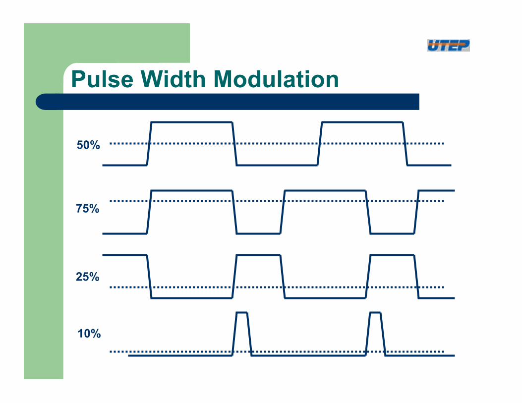
Pulse Width Modulation
50%
75%
25%
10%
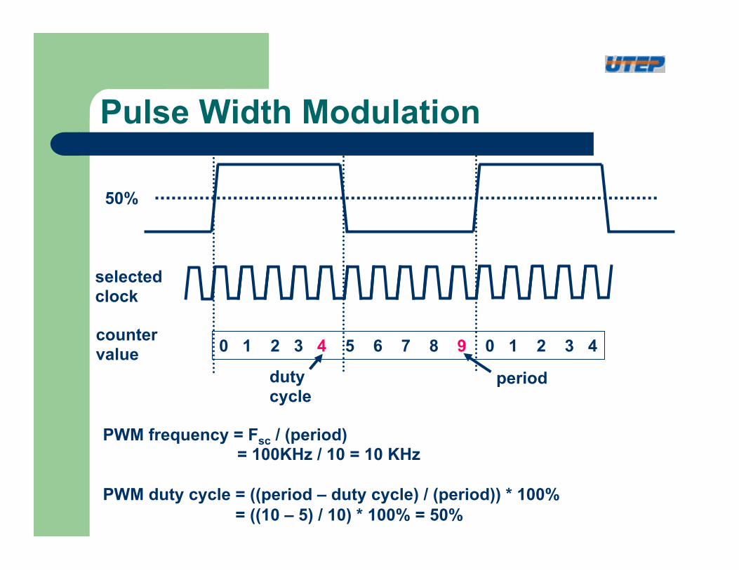
Pulse Width Modulation
50%
selected clock
counter value 0 1 2 3 4 5 6 7 8 9 0 1 2 3 4
duty cycle
period
PWM frequency = Fsc / (period) = 100KHz / 10 = 10 KHz
PWM duty cycle = ((period – duty cycle) / (period)) * 100%
= ((10 – 5) / 10) * 100% = 50%
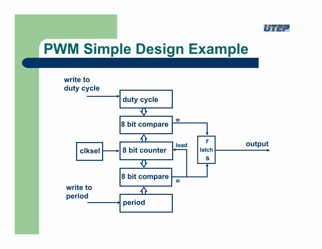
PWM Simple Design Example
8 bit counter
duty cycle
period
8 bit compare
8 bit compare
write to duty cycle
write to period
clksel output
=
=
load latch
r
s
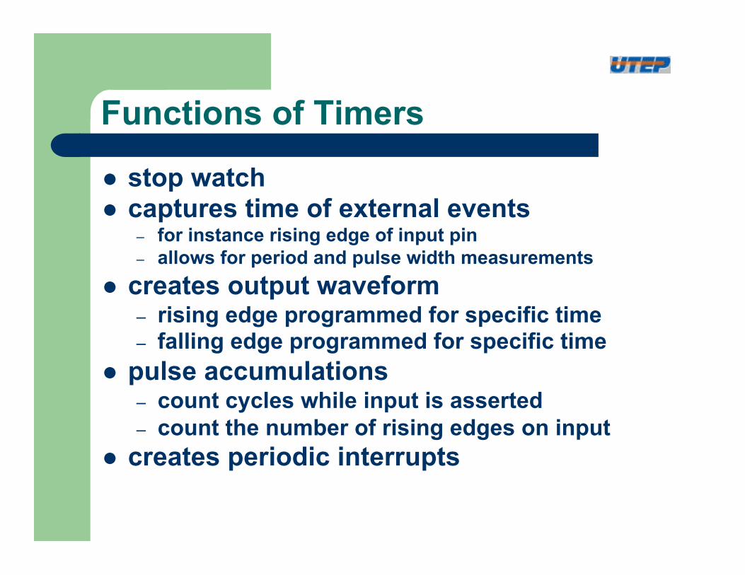
Functions of Timers
l stop watch l captures time of external events
– for instance rising edge of input pin – allows for period and pulse width measurements
l creates output waveform – rising edge programmed for specific time – falling edge programmed for specific time
l pulse accumulations – count cycles while input is asserted – count the number of rising edges on input
l creates periodic interrupts
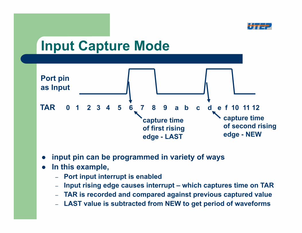
Input Capture Mode
TAR 0 1 2 3 4 5 6 7 8 9 a b c d e f 10 11 12
capture time of first rising edge - LAST
capture time of second rising edge - NEW
l input pin can be programmed in variety of ways l In this example,
– Port input interrupt is enabled – Input rising edge causes interrupt – which captures time on TAR – TAR is recorded and compared against previous captured value – LAST value is subtracted from NEW to get period of waveforms
Port pin as Input
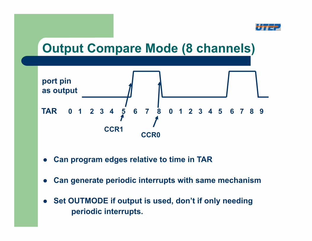
Output Compare Mode (8 channels)
TAR 0 1 2 3 4 5 6 7 8 0 1 2 3 4 5 6 7 8 9
CCR1 CCR0
l Can program edges relative to time in TAR l Can generate periodic interrupts with same mechanism
l Set OUTMODE if output is used, don’t if only needing periodic interrupts.
port pin as output
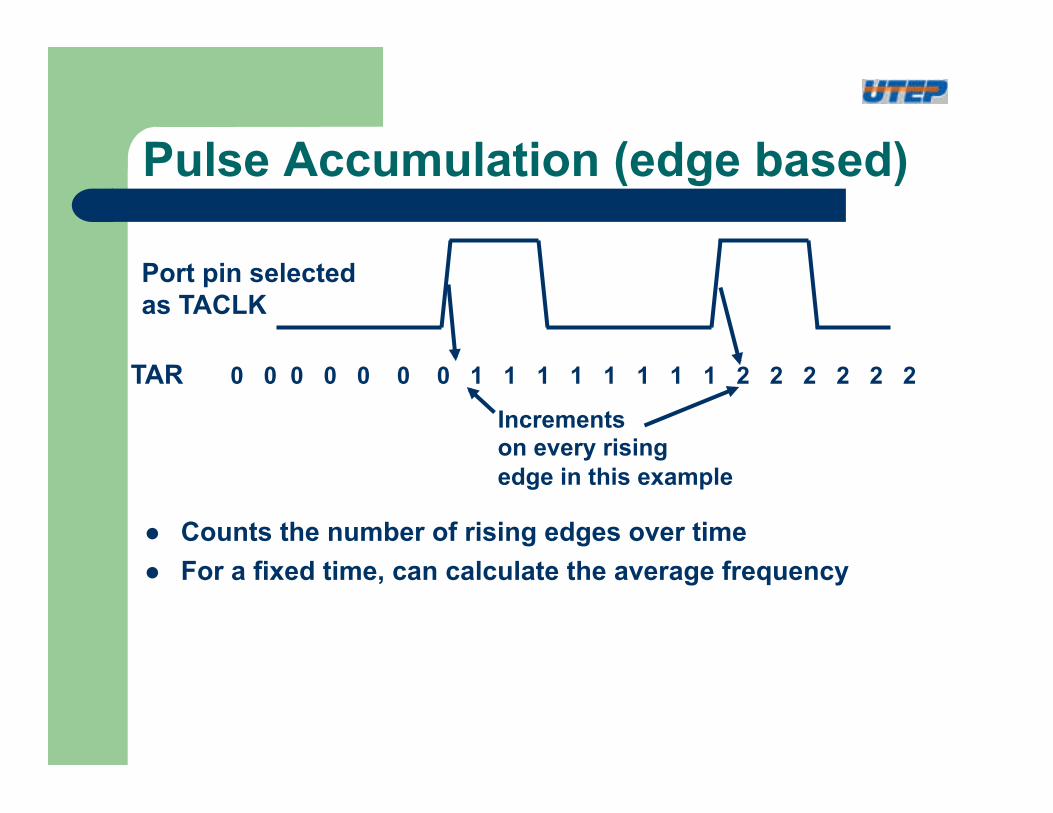
Pulse Accumulation (edge based)
TAR 0 0 0 0 0 0 0 1 1 1 1 1 1 1 1 2 2 2 2 2 2
Increments on every rising edge in this example
l Counts the number of rising edges over time l For a fixed time, can calculate the average frequency
Port pin selected as TACLK
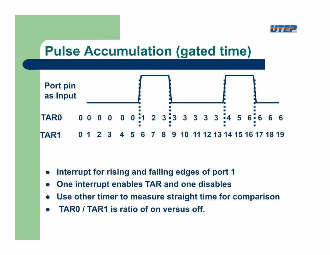
Pulse Accumulation (gated time)
TAR0 0 0 0 0 0 0 1 2 3 3 3 3 3 3 4 5 6 6 6 6
l Interrupt for rising and falling edges of port 1 l One interrupt enables TAR and one disables l Use other timer to measure straight time for comparison l TAR0 / TAR1 is ratio of on versus off.
Port pin as Input
TAR1 0 1 2 3 4 5 6 7 8 9 10 11 12 13 14 15 16 17 18 19
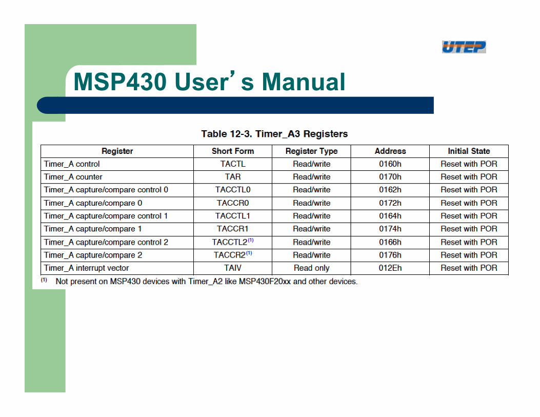
MSP430 User’s Manual
MSP430 User’s Manual
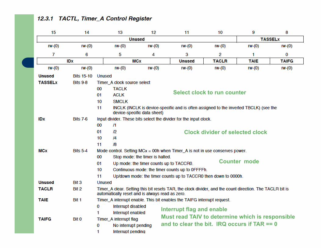
Select clock to run counter
Clock divider of selected clock
Counter mode
Interrupt flag and enable Must read TAIV to determine which is responsible and to clear the bit. IRQ occurs if TAR == 0
MSP430 User’s Manual
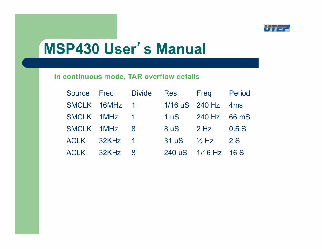
Source Freq Divide Res Freq Period SMCLK 16MHz 1 1/16 uS 240 Hz 4ms SMCLK 1MHz 1 1 uS 240 Hz 66 mS SMCLK 1MHz 8 8 uS 2 Hz 0.5 S ACLK 32KHz 1 31 uS ½ Hz 2 S ACLK 32KHz 8 240 uS 1/16 Hz 16 S
In continuous mode, TAR overflow details
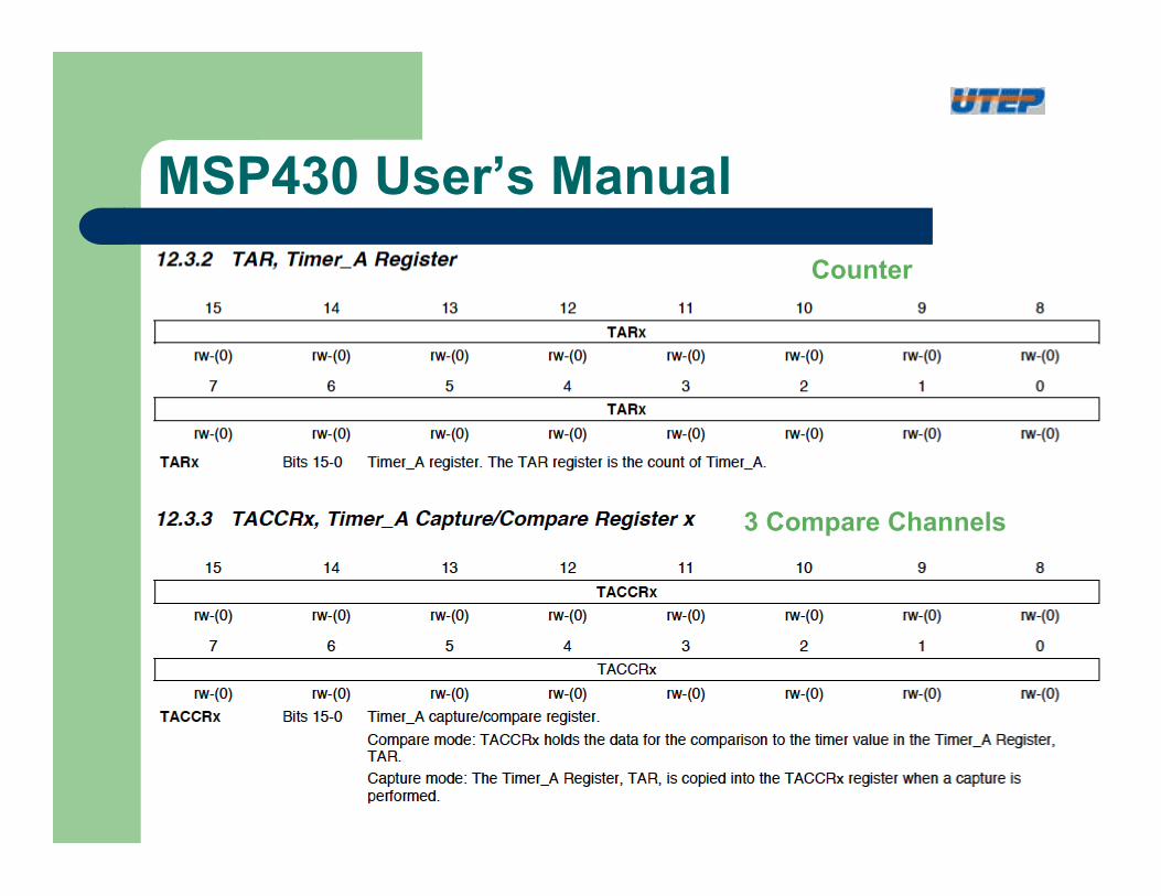
MSP430 User’s Manual Counter
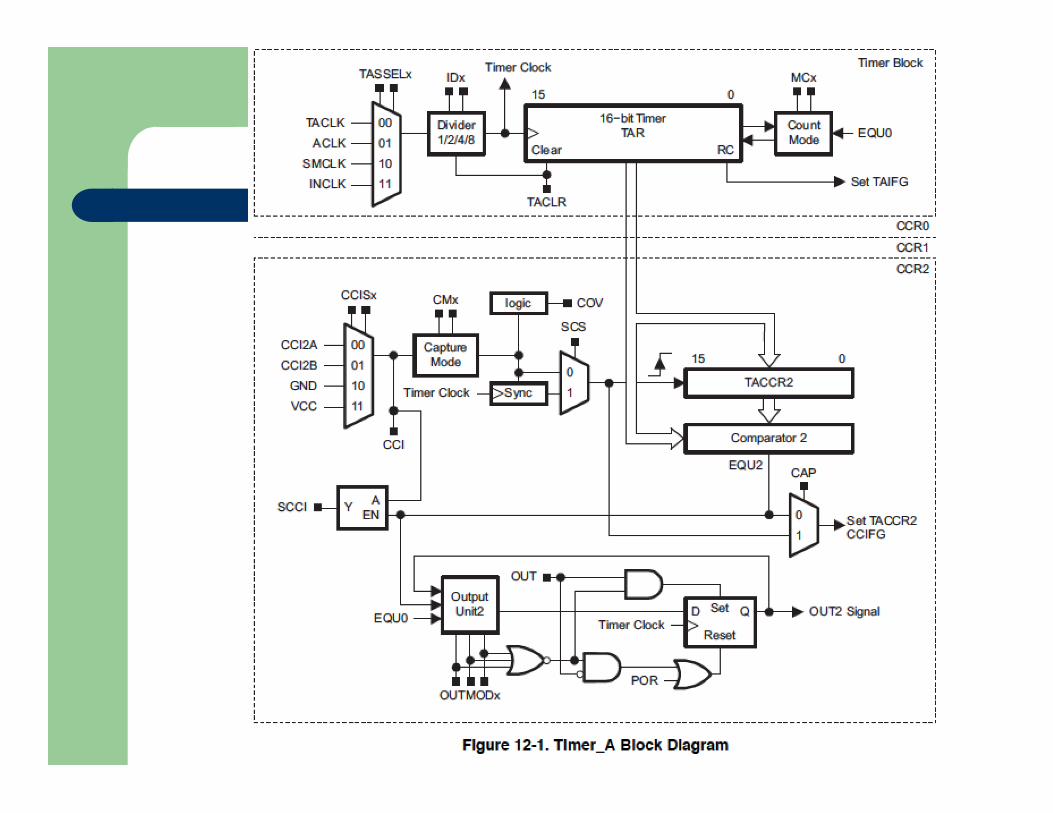
3 Compare Channels
MSP430 User’s Manual
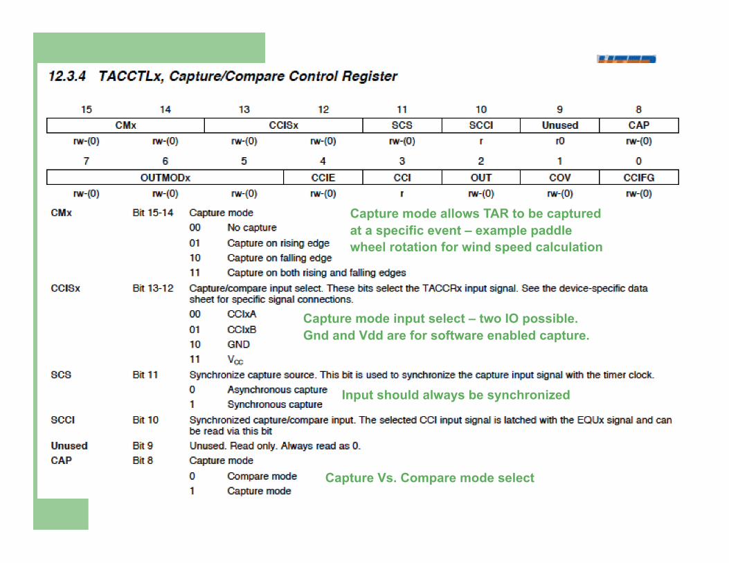
Capture mode allows TAR to be captured at a specific event – example paddle wheel rotation for wind speed calculation
Capture mode input select – two IO possible. Gnd and Vdd are for software enabled capture.
Capture Vs. Compare mode select
Input should always be synchronized
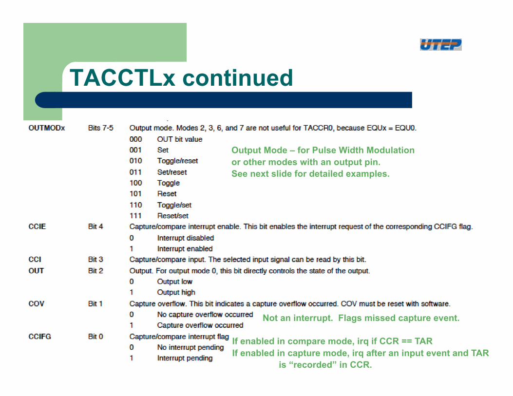
TACCTLx continued
Output Mode – for Pulse Width Modulation or other modes with an output pin. See next slide for detailed examples.
Not an interrupt. Flags missed capture event.
If enabled in compare mode, irq if CCR == TAR If enabled in capture mode, irq after an input event and TAR
is “recorded” in CCR.
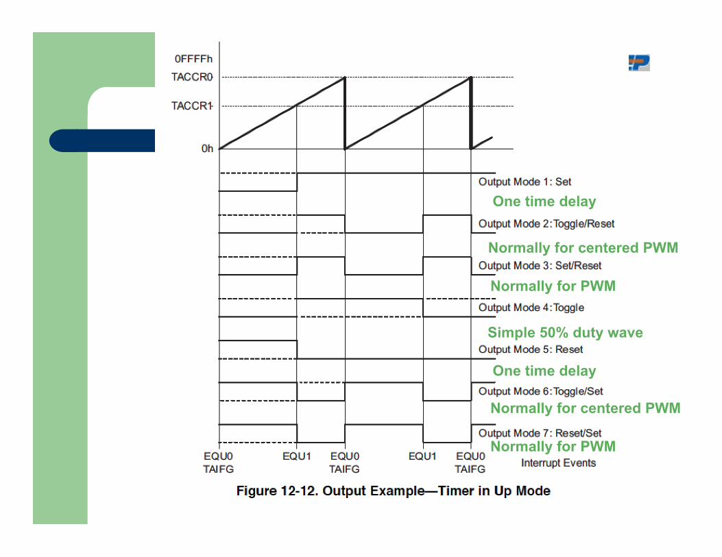
One time delay
Normally for centered PWM
Normally for centered PWM
Normally for PWM
Normally for PWM
Simple 50% duty wave
One time delay
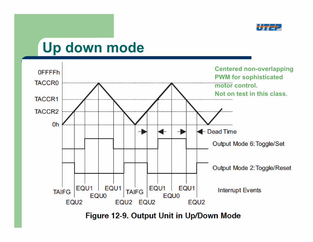
Up down mode Centered non-overlapping PWM for sophisticated motor control. Not on test in this class.
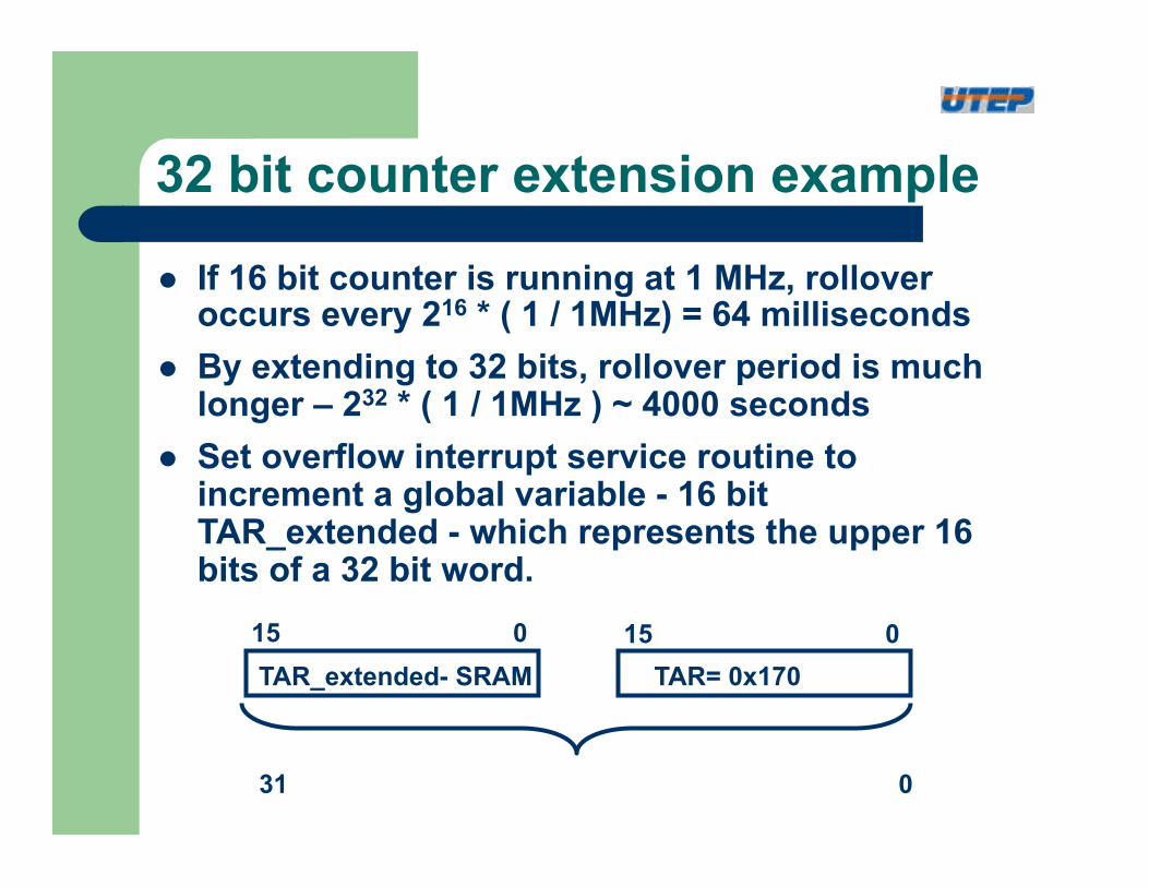
32 bit counter extension example
l If 16 bit counter is running at 1 MHz, rollover occurs every 216 * ( 1 / 1MHz) = 64 milliseconds
l By extending to 32 bits, rollover period is much longer – 232 * ( 1 / 1MHz ) ~ 4000 seconds
l Set overflow interrupt service routine to increment a global variable - 16 bit TAR_extended - which represents the upper 16 bits of a 32 bit word.
TAR= 0x170 TAR_extended- SRAM 15 0 15 0
31 0
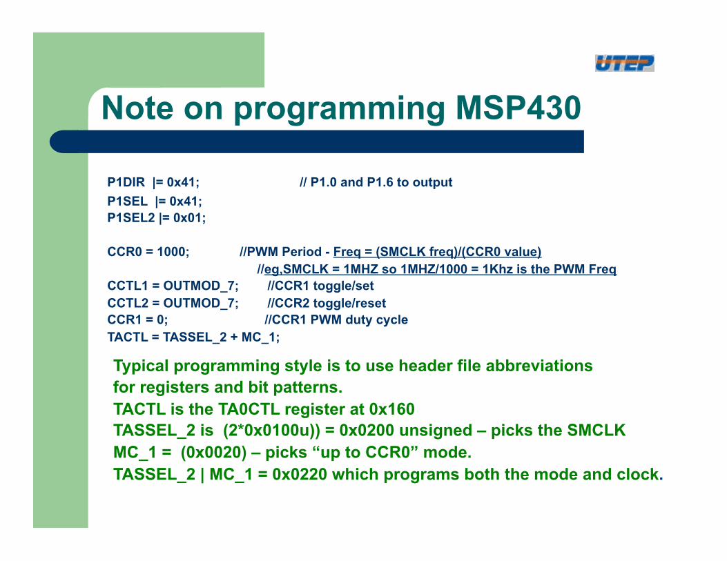
Note on programming MSP430
P1DIR |= 0x41; // P1.0 and P1.6 to output P1SEL |= 0x41; P1SEL2 |= 0x01;
CCR0 = 1000; //PWM Period - Freq = (SMCLK freq)/(CCR0 value) //eg,SMCLK = 1MHZ so 1MHZ/1000 = 1Khz is the PWM Freq CCTL1 = OUTMOD_7; //CCR1 toggle/set CCTL2 = OUTMOD_7; //CCR2 toggle/reset CCR1 = 0; //CCR1 PWM duty cycle TACTL = TASSEL_2 + MC_1;
Typical programming style is to use header file abbreviations for registers and bit patterns. TACTL is the TA0CTL register at 0x160 TASSEL_2 is (2*0x0100u)) = 0x0200 unsigned – picks the SMCLK MC_1 = (0x0020) – picks “up to CCR0” mode. TASSEL_2 | MC_1 = 0x0220 which programs both the mode and clock.
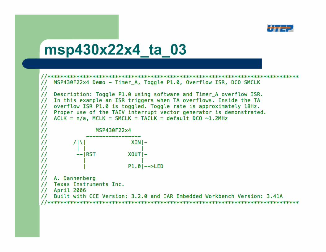
msp430x22x4_ta_03
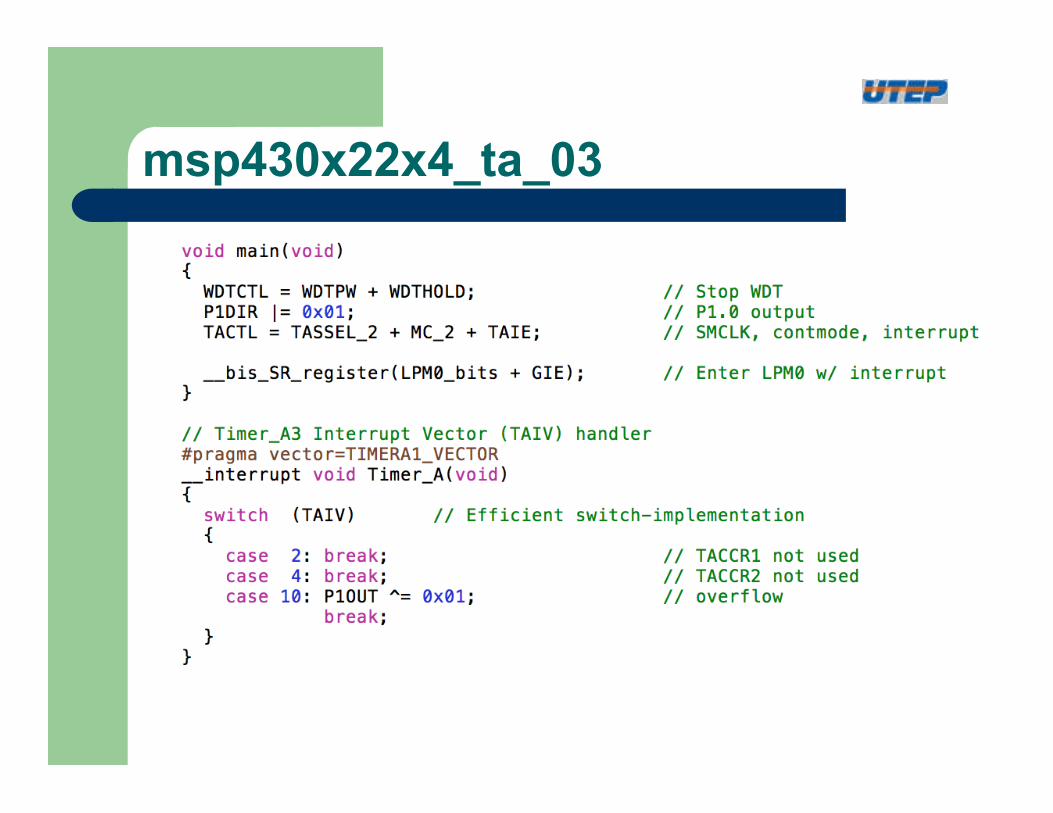
msp430x22x4_ta_03
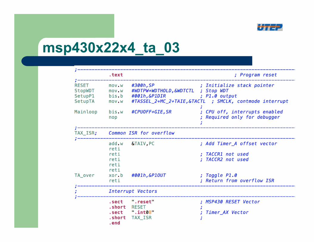
msp430x22x4_ta_03
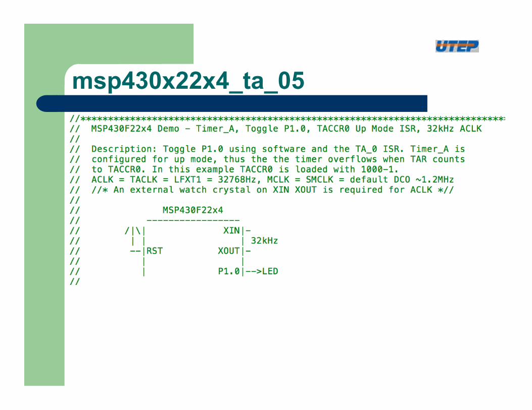
msp430x22x4_ta_05
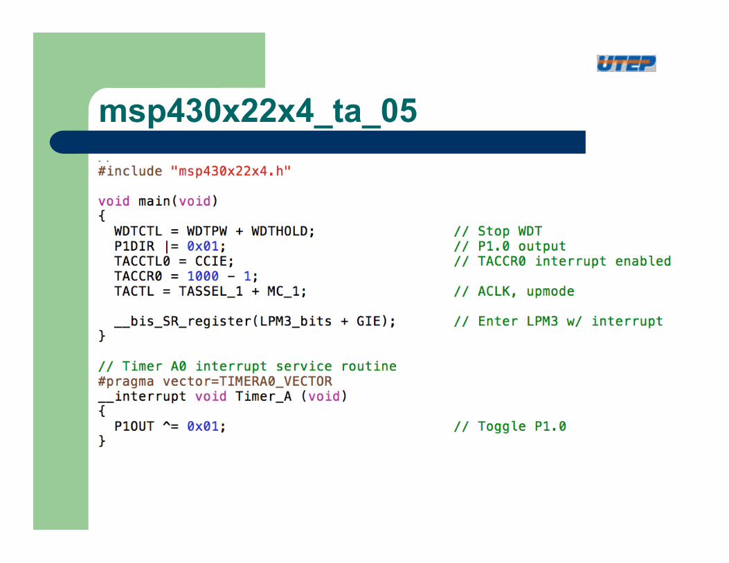
msp430x22x4_ta_05
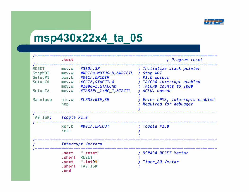
msp430x22x4_ta_05
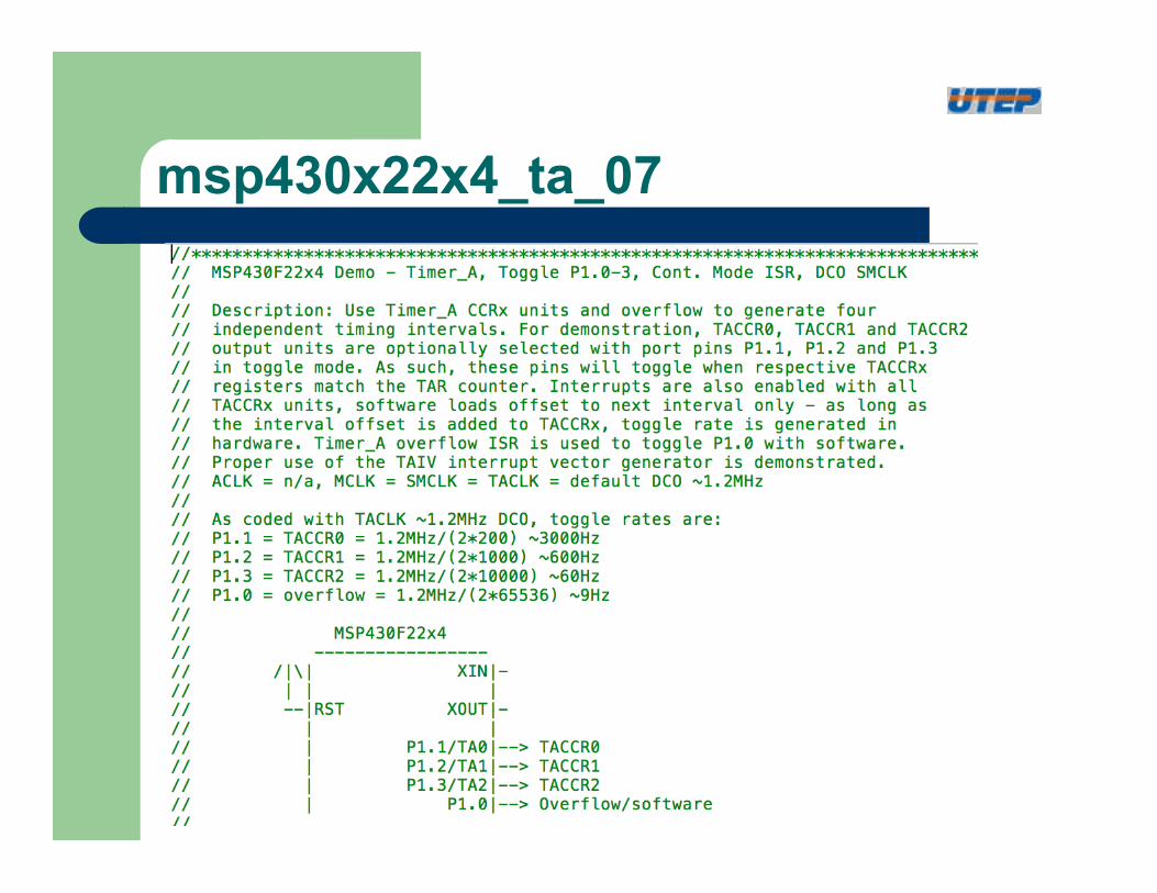
msp430x22x4_ta_07
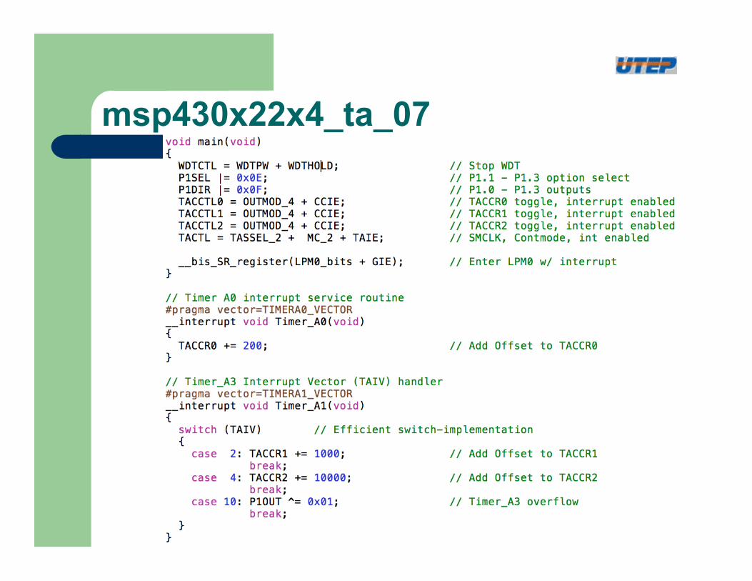
msp430x22x4_ta_07
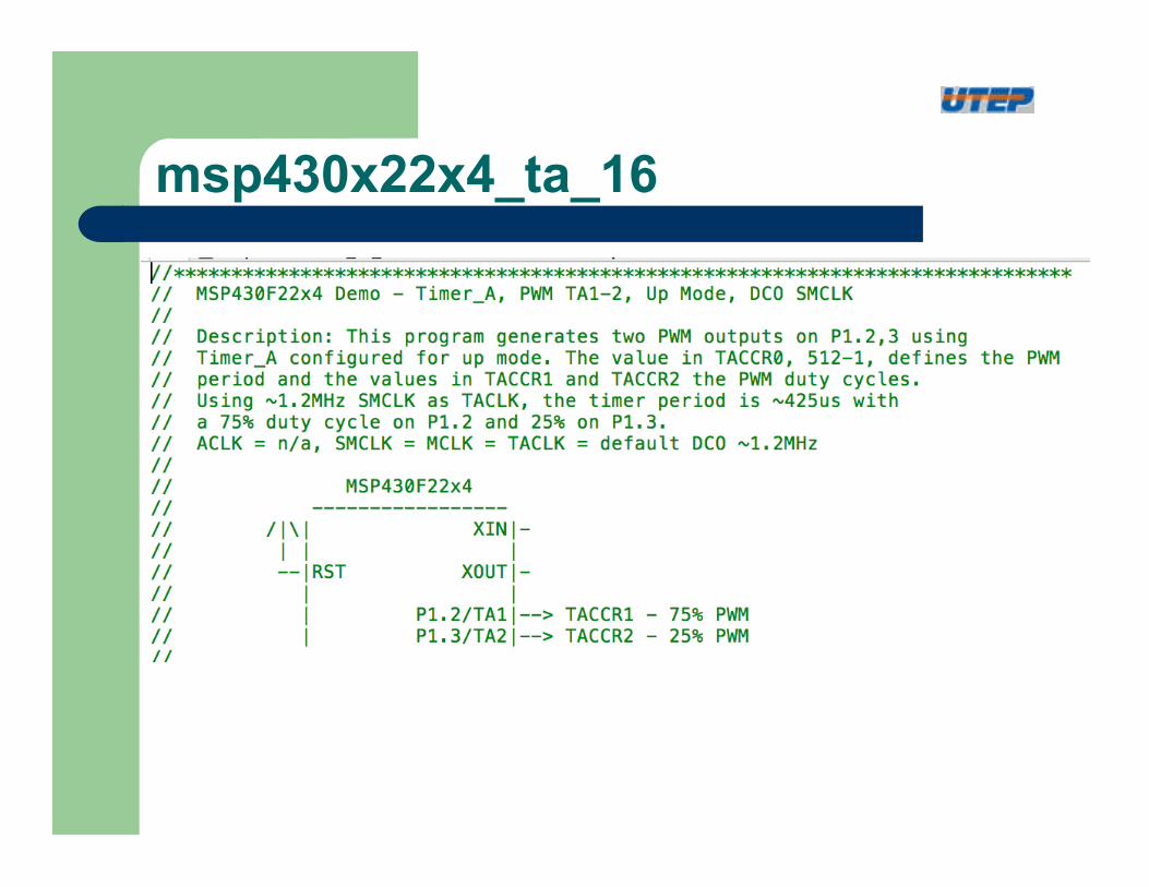
msp430x22x4_ta_16
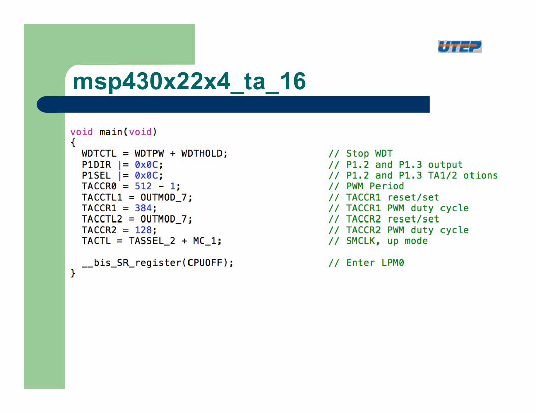
msp430x22x4_ta_16
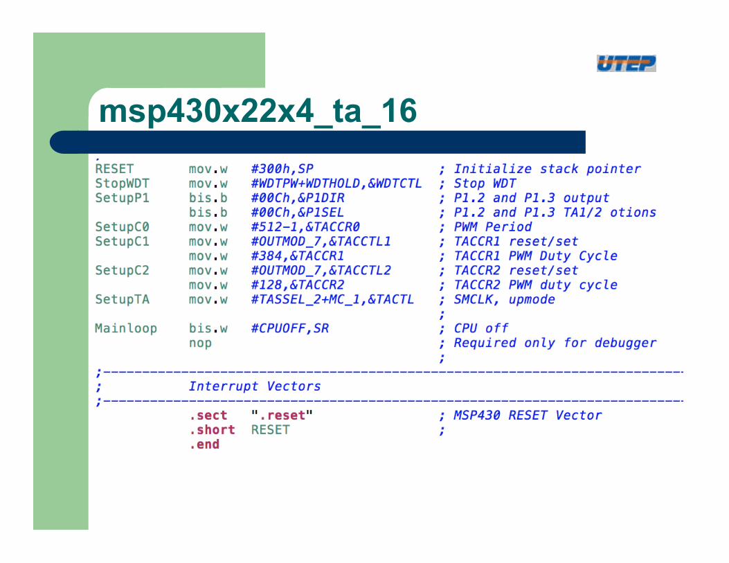
msp430x22x4_ta_16
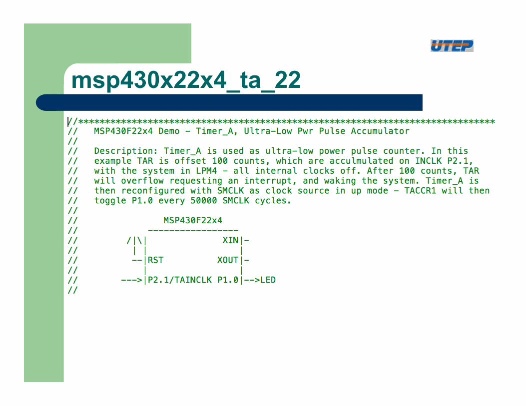
msp430x22x4_ta_22
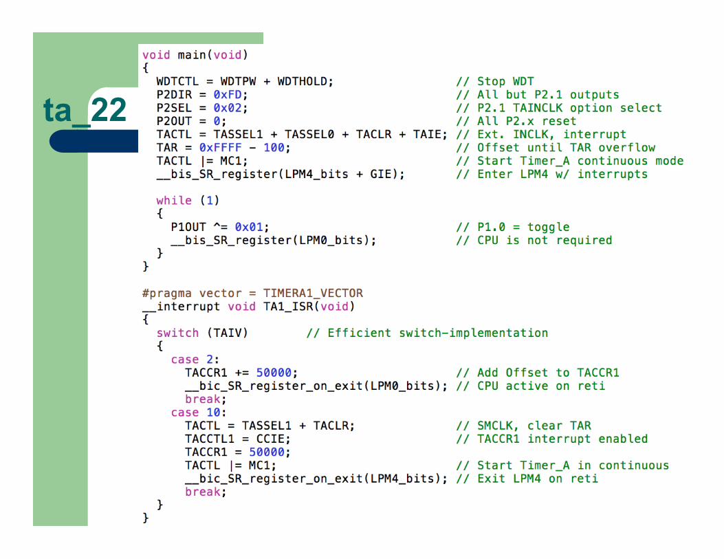
ta_22