Embed Size (px)
Citation preview

EE415 VLSI Design
Notices•You have 18 more days to complete your final project!•Collaborate with each other (NOT Copy!!)•Presentations will be held on March 7 (Tuesday) and March 9 (Thursday) In Rm. 301 During Lab Hours•Magiboard, Projector, Notebook PC will be available to you•Use the Color Printer!
EE415 VLSI Design
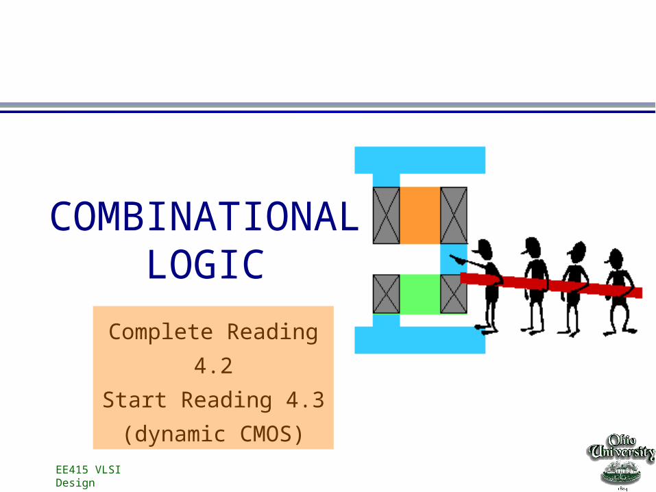
Complete Reading
4.2
Start Reading 4.3
(dynamic CMOS)
COMBINATIONAL LOGIC
EE415 VLSI Design
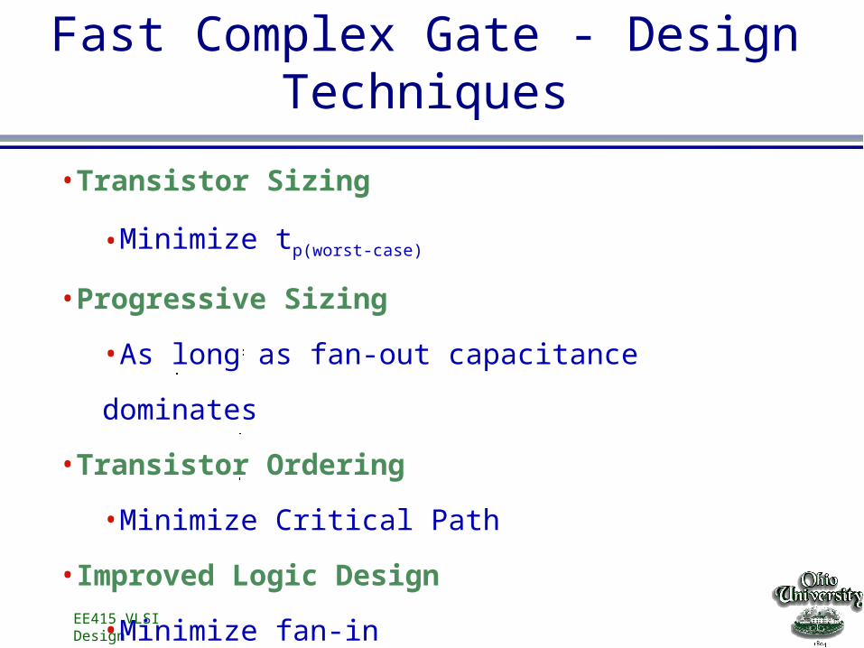
Fast Complex Gate - Design Techniques
•Transistor Sizing
•Minimize tp(worst-case)
•Progressive Sizing
•As long as fan-out capacitance dominates
•Transistor Ordering
•Minimize Critical Path
•Improved Logic Design
•Minimize fan-in
EE415 VLSI Design
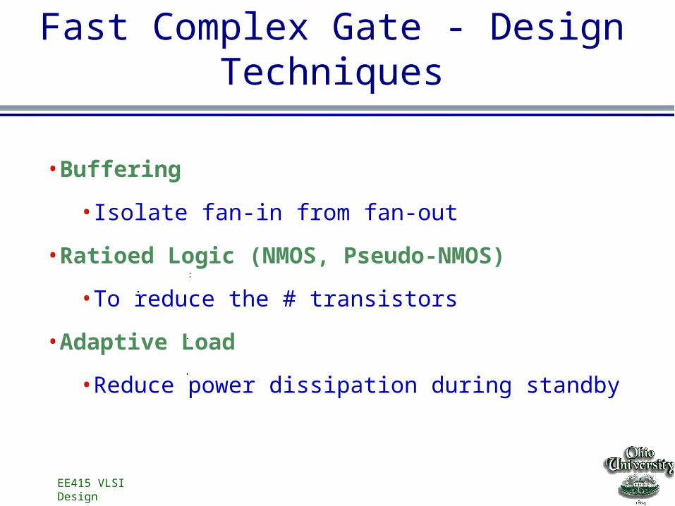
Fast Complex Gate - Design Techniques
•Buffering
•Isolate fan-in from fan-out
•Ratioed Logic (NMOS, Pseudo-NMOS)
•To reduce the # transistors
•Adaptive Load
•Reduce power dissipation during standby
EE415 VLSI Design
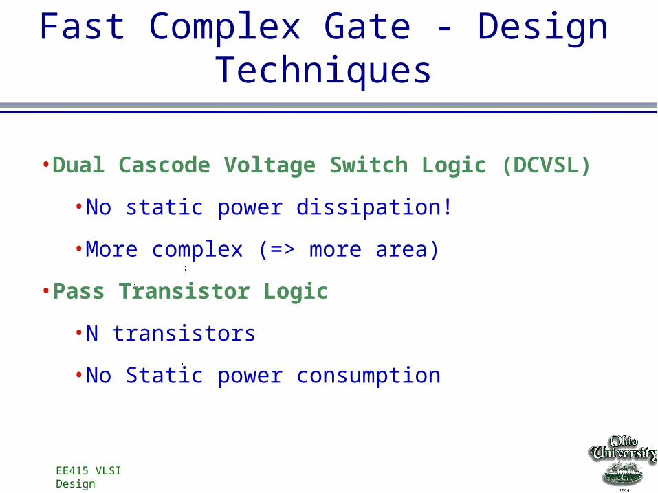
Fast Complex Gate - Design Techniques
•Dual Cascode Voltage Switch Logic (DCVSL)
•No static power dissipation!
•More complex (=> more area)
•Pass Transistor Logic
•N transistors
•No Static power consumption
EE415 VLSI Design
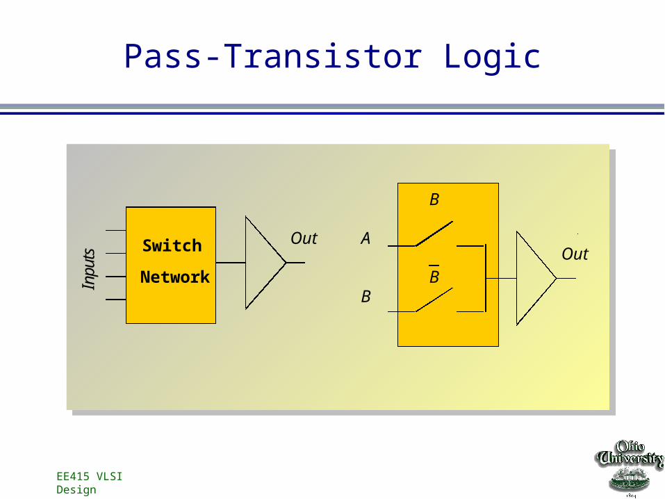
Pass-Transistor LogicIn
puts Switch
Network
OutOut
A
B
B
B
EE415 VLSI Design
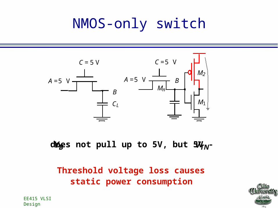
NMOS-only switch
A = 5 V
B
C = 5 V
CL
A = 5 V
C = 5 V
BM2
M1
Mn
Threshold voltage loss causesstatic power consumption
VB does not pull up to 5V, but 5V - VTN
EE415 VLSI Design
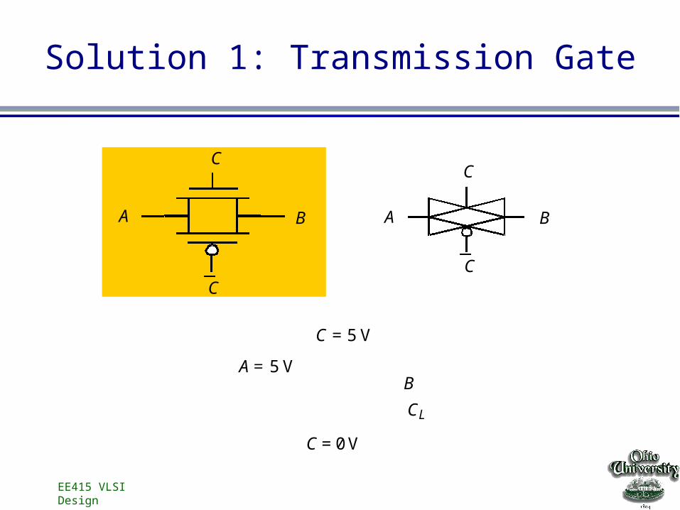
Solution 1: Transmission Gate
A B
C
C
A B
C
C
B
CL
C = 0 V
A = 5 V
C = 5 V
EE415 VLSI Design
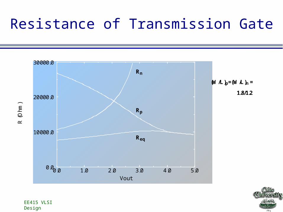
Resistance of Transmission Gate
(W/L)p=(W/L)n =
1.8/1.2
0.0 1.0 2.0 3.0 4.0 5.0Vout
0.0
10000.0
20000.0
30000.0
R (
Ohm
)
Rn
Req
Rp
EE415 VLSI Design
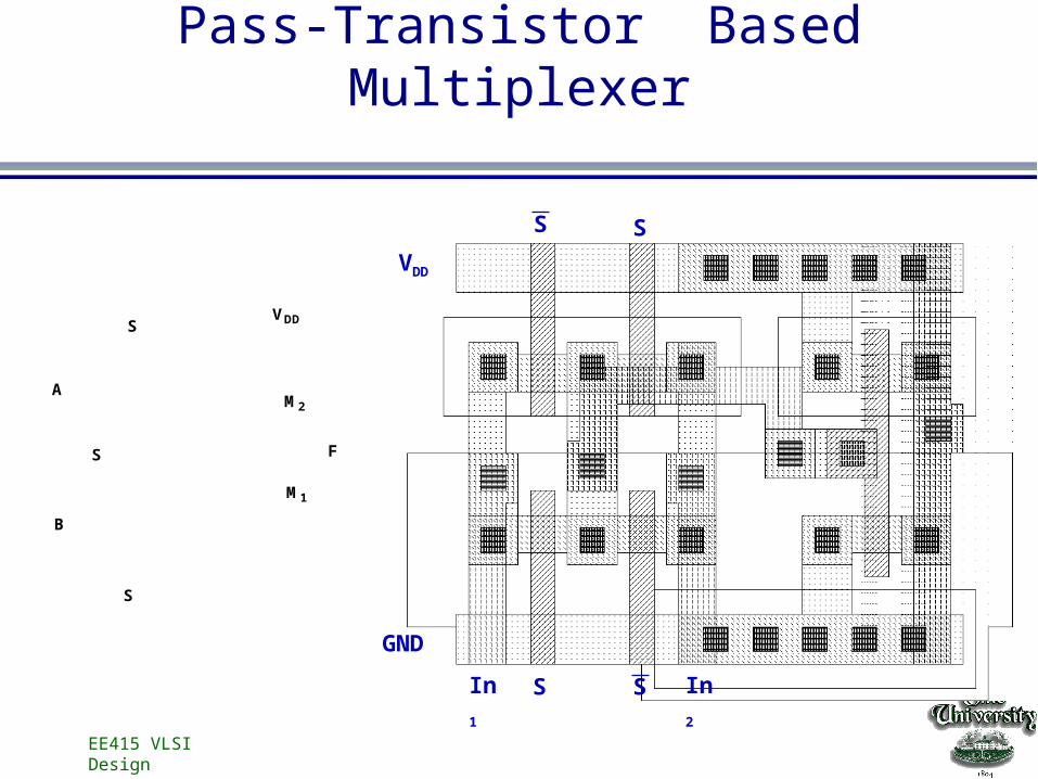
Pass-Transistor Based Multiplexer
AM2
M1
B
S
S
S F
VDD
GND
VDD
In1
In2
S S
S S
EE415 VLSI Design
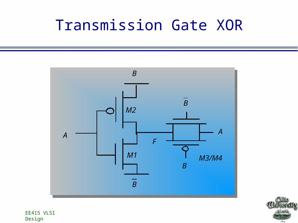
Transmission Gate XOR
A
B
F
B
A
B
B
M1
M2
M3/M4
EE415 VLSI Design
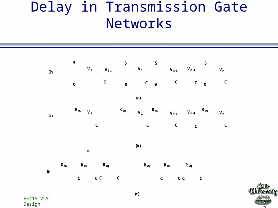
Delay in Transmission Gate Networks
V1 Vi -1
C
5 5
0 0
Vi Vi+1
CC
5
0
Vn-1 Vn
CC
5
0
In
V1 Vi Vi+1
C
Vn-1 Vn
CC
In
ReqReq Req Req
CC
(a)
(b)
C
Req Req
C C
Req
C C
Req Req
C C
Req
C
In
m
(c)
EE415 VLSI Design
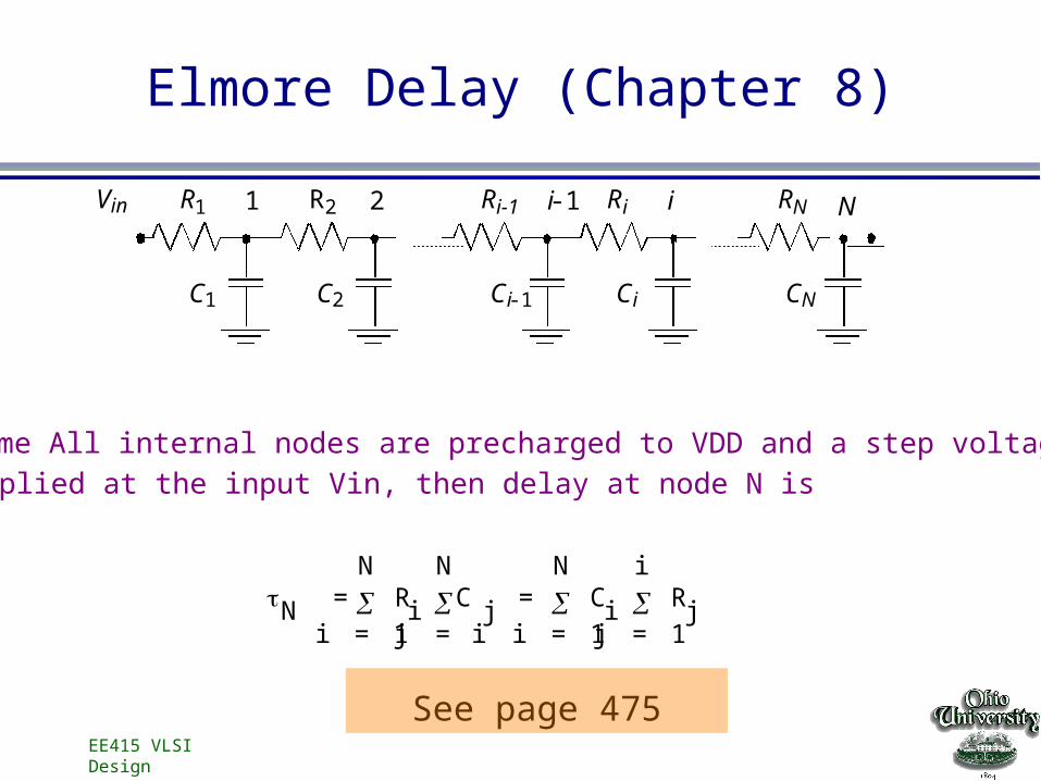
Elmore Delay (Chapter 8)
R1
C1
R2
C2
Ri-1
Ci-1
Ri
Ci
RN
CN
Vin N1 2 i-1 i
Assume All internal nodes are precharged to VDD and a step voltage is
applied at the input Vin, then delay at node N is
N Ri C =jj i=
N
i 1=
N
Ci Rjj 1=
i
i 1=
N
=
See page 475
EE415 VLSI Design
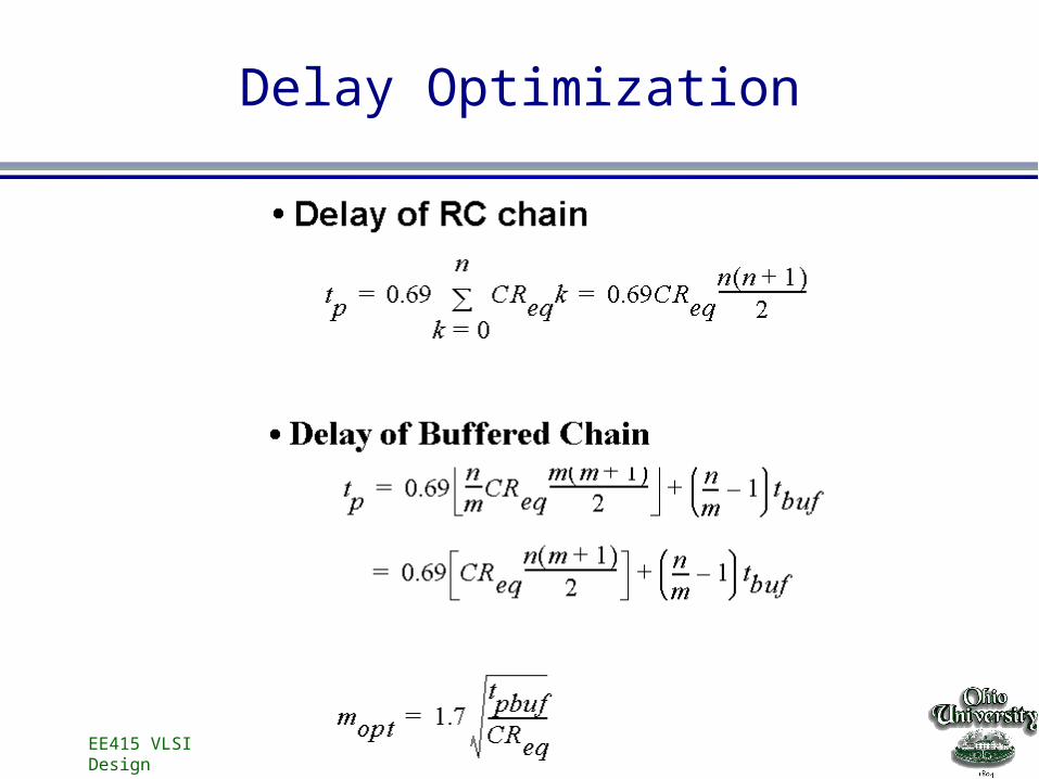
Delay Optimization
EE415 VLSI Design
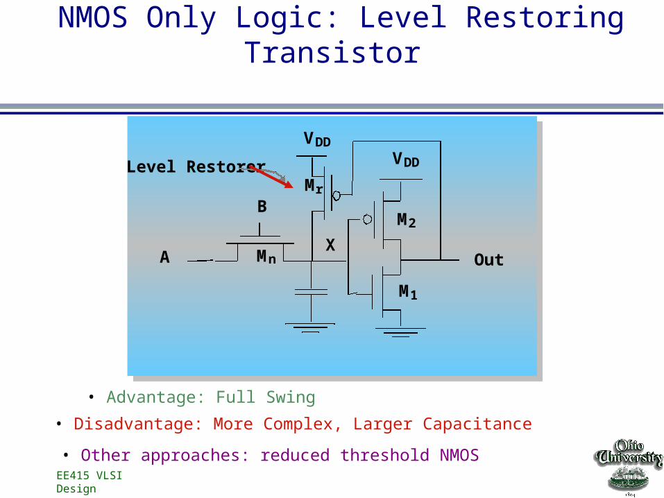
NMOS Only Logic: Level Restoring Transistor
M2
M1
Mn
Mr
OutA
B
VDDVDDLevel Restorer
X
• Advantage: Full Swing
• Disadvantage: More Complex, Larger Capacitance
• Other approaches: reduced threshold NMOS
EE415 VLSI Design
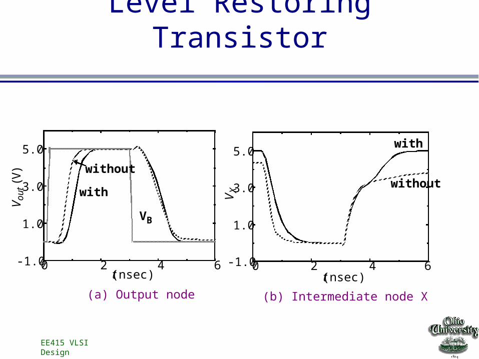
Level Restoring Transistor
(a) Output node (b) Intermediate node X
0 2 4 6t (nsec)
-1.0
1.0
3.0
5.0
Vo
ut (
V)
0 2 4t (nsec)
-1.0
1.0
3.0
5.0
VX
with
without
VB
with
without
6
EE415 VLSI Design
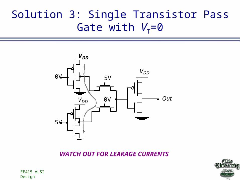
Solution 3: Single Transistor Pass Gate with VT=0
Out
VDD
VDD
5V
VDD
0V 5V
0V
WATCH OUT FOR LEAKAGE CURRENTS
EE415 VLSI Design
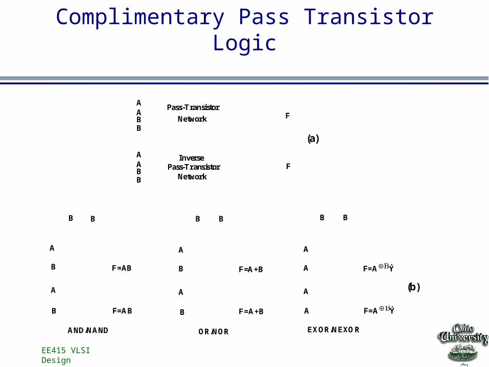
Complimentary Pass Transistor Logic
A
B
A
B
B B B B
A
B
A
B
F=AB
F=AB
F=A+B
F=A+B
B B
A
A
A
A
F=AÝ
F=AÝ
OR/NOR EXOR/NEXORAND/NAND
F
F
Pass-Transistor
Network
Pass-TransistorNetwork
AABB
AABB
Inverse
(a)
(b)
EE415 VLSI Design
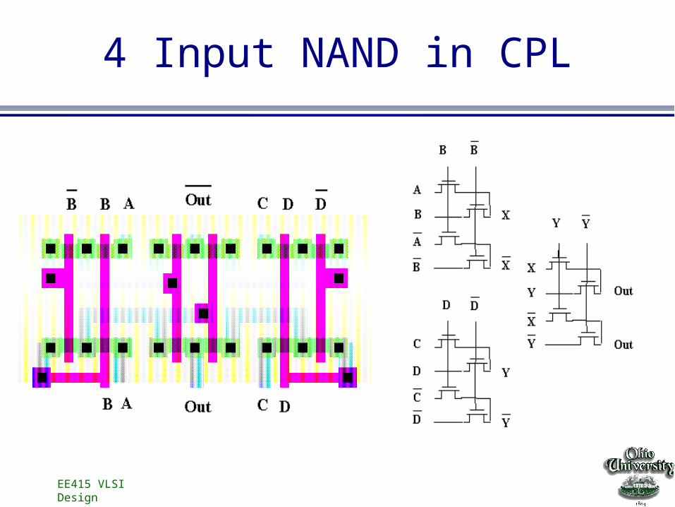
4 Input NAND in CPL
EE415 VLSI Design
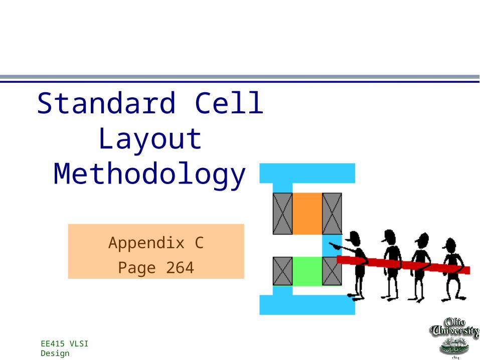
Appendix C
Page 264
Standard Cell Layout
Methodology
EE415 VLSI Design
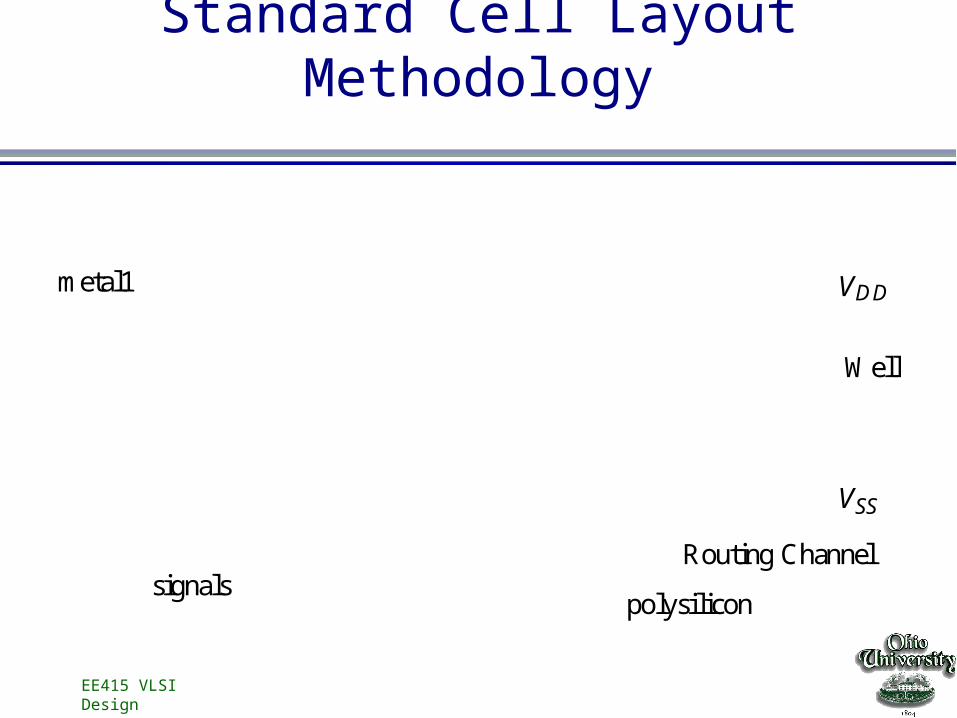
Standard Cell Layout Methodology
VDD
VSS
Well
signalsRouting Channel
metal1
polysilicon
EE415 VLSI Design
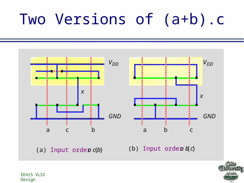
Two Versions of (a+b).c
a c b a b c
xx
GND
VDDVDD
GND
(a) Input order { a c b} (b) Input order { a b c}
EE415 VLSI Design
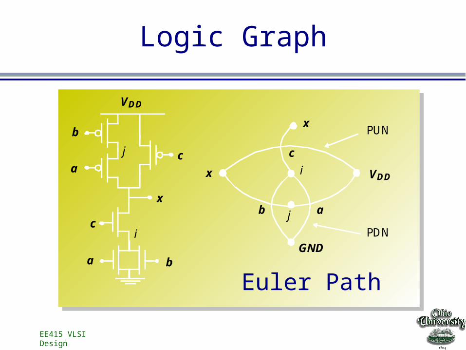
Logic Graph
VDD
c
a
x
b
ca
b
GND
x
VDDx
c
b a
i
j
i
j
PDN
PUN
Euler Path
EE415 VLSI Design
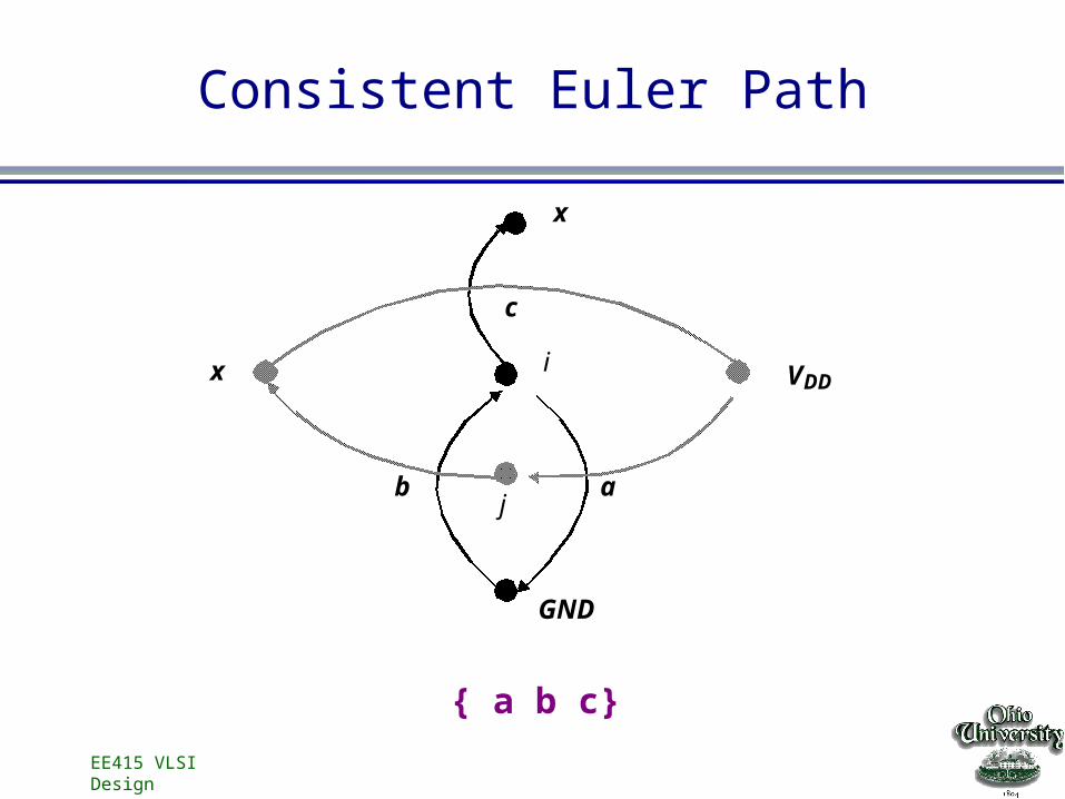
Consistent Euler Path
GND
x
VDDx
c
b a
i
j
{ a b c}
EE415 VLSI Design
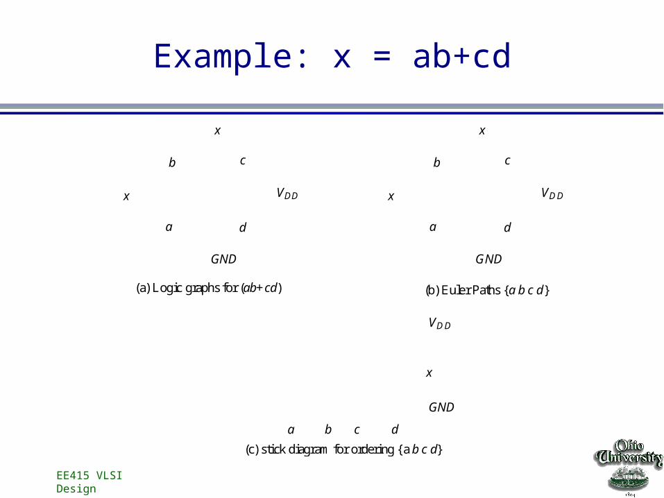
Example: x = ab+cd
GND
x
a
b c
d
VDDx
GND
x
a
b c
d
VDDx
(a) Logic graphs for (ab+cd) (b) Euler Paths {a b c d}
a c d
x
VDD
GND
(c) stick diagram for ordering {a b c d}
b
EE415 VLSI Design
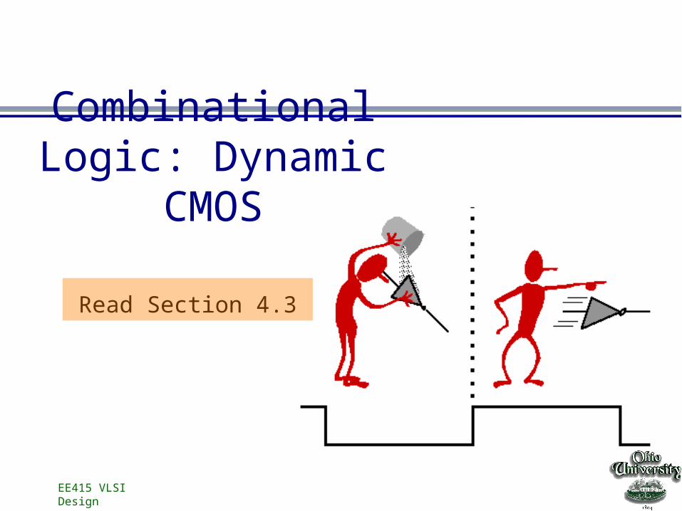
Read Section 4.3
Combinational Logic: Dynamic
CMOS
EE415 VLSI Design
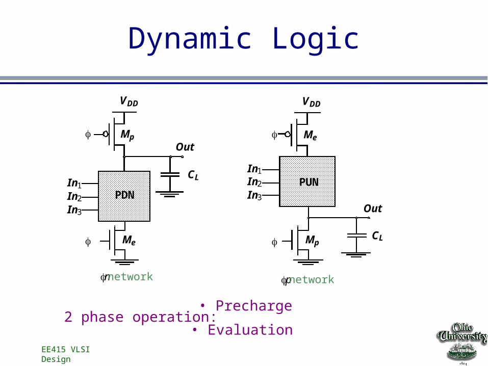
Dynamic Logic
Mp
Me
VDD
PDN
In1
In2
In3
OutMe
Mp
VDD
PUN
In1
In2
In3
Out
CL
CL
p networkn network
2 phase operation:• Evaluation
• Precharge
EE415 VLSI Design
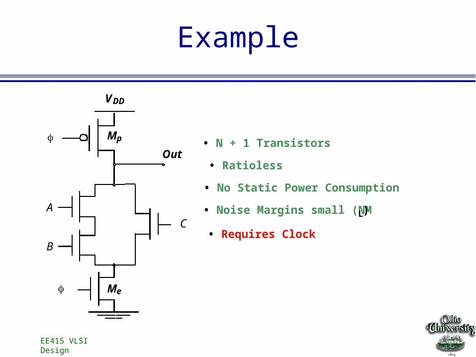
Example
Mp
Me
VDD
Out
A
B
C
• N + 1 Transistors
• Ratioless
• No Static Power Consumption
• Noise Margins small (NML)
• Requires Clock
EE415 VLSI Design
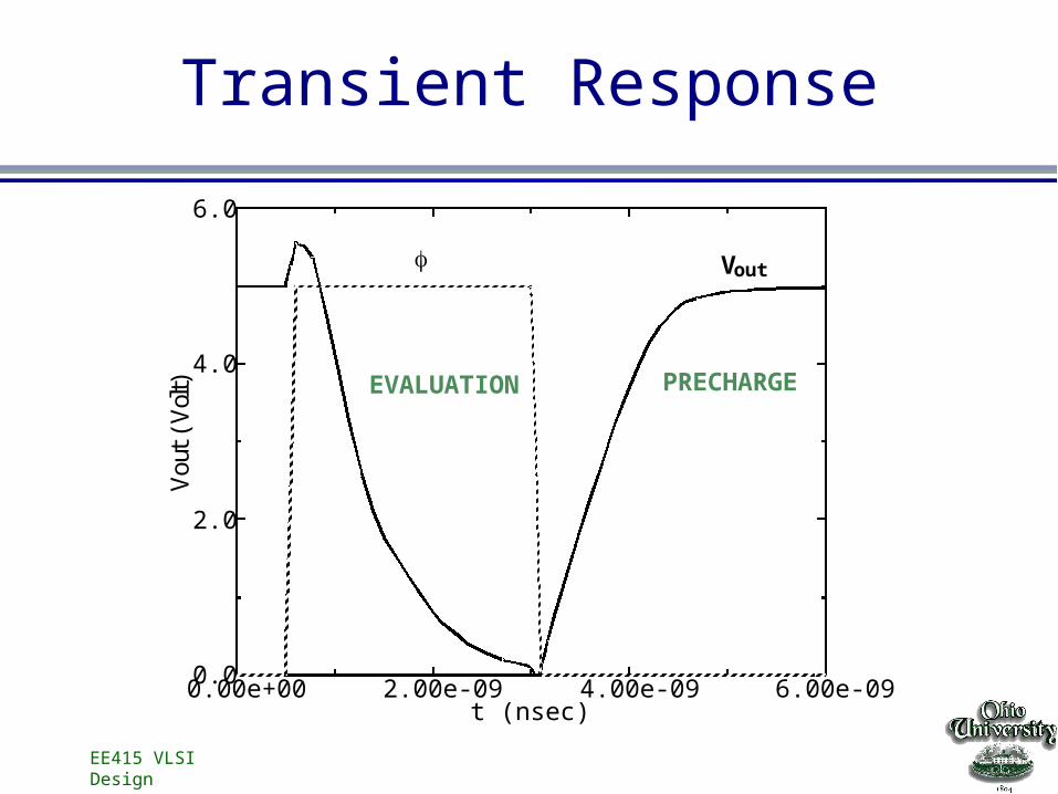
Transient Response
0.00e+00 2.00e-09 4.00e-09 6.00e-09t (nsec)
0.0
2.0
4.0
6.0V
out
(Vol
t)
Vout
PRECHARGEEVALUATION
EE415 VLSI Design
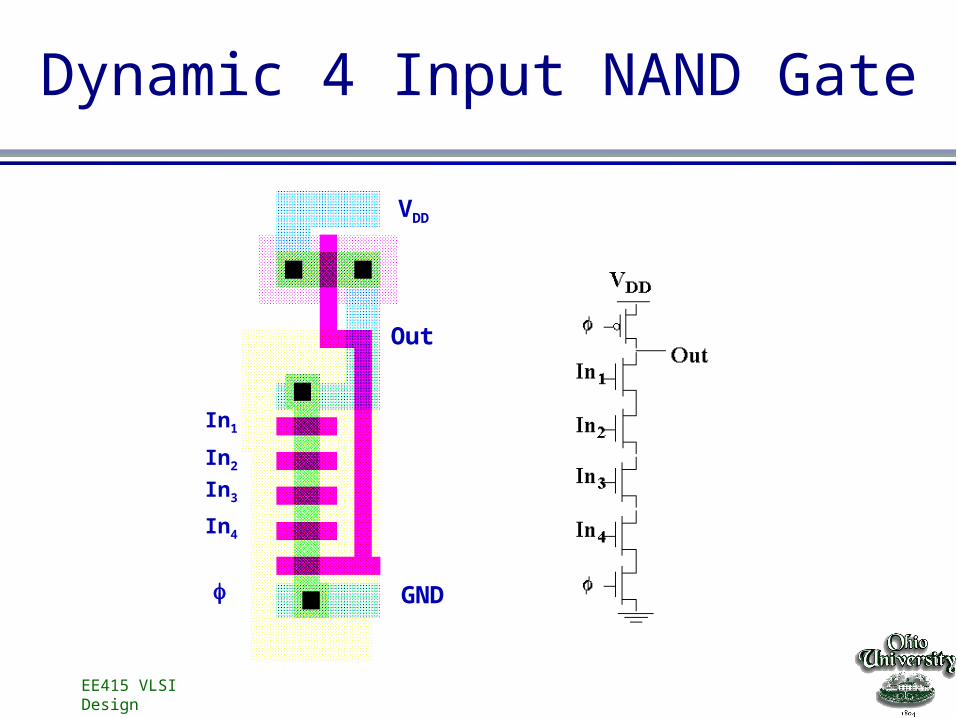
Dynamic 4 Input NAND Gate
In1
In2
In3
In4
Out
VDD
GND

![EE415 VLSI Design The Devices: Diode [Adapted from Rabaey’s Digital Integrated Circuits, ©2002, J. Rabaey et al.]](https://img.pdfslide.net/doc/110x75/56649dca5503460f94ac0749/ee415-vlsi-design-the-devices-diode-adapted-from-rabaeys-digital-integrated.jpg)


![EE415 VLSI Design THE INVERTER [Adapted from Rabaey’s Digital Integrated Circuits, ©2002, J. Rabaey et al.]](https://img.pdfslide.net/doc/110x75/56649ea35503460f94ba7dea/ee415-vlsi-design-the-inverter-adapted-from-rabaeys-digital-integrated.jpg)

![EE415 VLSI Design COMBINATIONAL LOGIC [Adapted from Rabaeys Digital Integrated Circuits, ©2002, J. Rabaey et al.]](https://img.pdfslide.net/doc/110x75/5519b7875503465b578b4854/ee415-vlsi-design-combinational-logic-adapted-from-rabaeys-digital-integrated-circuits-2002-j-rabaey-et-al.jpg)