Embed Size (px)
Citation preview

VALLIAMMAI ENGINEERING COLLEGE SRM NAGAR, KATTANKULATHUR – 603203
EE8261-ELECTRIC CIRCUITS LABORATORY
LABORATORY MANUAL
1ST YEAR – EEE (REGULATION2017)
Preparedby,
DEPARTMENT OF ELECTRICAL AND ELECTRONICS
ENGINEERING
Mr. RAGUL KUMAR K., A.P (O.G),
Mrs. Ms.R.V.PREETHA A.P (O.G),


1
EE8261 ELECTRIC CIRCUITS LABORATORY L T P C 0 0 4 2 LIST OF EXPERIMENTS
1. Simulation and experimental verification of electrical circuit problems using Kirchhoff’s voltage and current laws.
2. Simulation and experimental verification of electrical circuit problems using Thevenin’s theorem.
3. Simulation and experimental verification of electrical circuit problems using Norton’s theorem.
4. Simulation and experimental verification of electrical circuit problems using Superposition theorem.
5. Simulation and experimental verification of Maximum Power transfer Theorem.
6. Study of Analog and digital oscilloscopes and measurement of sinusoidal voltage, frequency and power factor.
7. Simulation and Experimental validation of R-C electric circuit transients. 8. Simulation and Experimental validation of frequency response of RLC electric
circuit. 9. Design and Simulation of series resonance circuit. 10. Design and Simulation of parallel resonant circuits. 11. Simulation of three phase balanced and unbalanced star, delta networks
circuits. TOTAL: 60 PERIODS LABORATORY REQUIREMENTS FOR BATCH OF 30 STUDENTS
1. Regulated Power Supply: 0 – 15 V D.C - 10 Nos / Distributed Power Source. 2. Function Generator (1 MHz) - 10 Nos. 3. Single Phase Energy Meter - 1 No. 4. Oscilloscope (20 MHz)-10 Nos. 5. Digital Storage Oscilloscope (20 MHz) – 1 No. 6. 10 Nos. of PC with Circuit Simulation Software (min 10 Users) ( e-Sim Scilab/
Pspice / MATLAB /other Equivalent software Package) and Printer (1 No.) 7. AC/DC - Voltmeters (10 Nos.), Ammeters (10 Nos.) and Multi-meters (10
Nos.) 8. Single Phase Wattmeter – 3 Nos. 9. Decade Resistance Box, Decade Inductance Box, Decade Capacitance Box - 6
Nos each. 10. Circuit Connection Boards - 10 Nos.
Necessary Resistors, Inductors, Capacitors of various quantities (Quarter Watt to 10 Watt).

EE6211-Electric Circuits Laboratory
2
EE8261 ELECTRIC CIRCUITS LABORATORY
Cycle – 1
1. Simulation and experimental verification of electrical circuit problems using
Kirchhoff’s voltage and current laws.
2. Simulation and experimental verification of electrical circuit problems using
Thevenin’s theorem.
3. Simulation and experimental verification of electrical circuit problems using
Norton’s theorem.
4. Simulation and experimental verification of electrical circuit problems using
Superposition theorem.
5. Simulation and experimental verification of Maximum Power transfer
Theorem.
6. Study of Analog and digital oscilloscopes and measurement of sinusoidal
voltage, frequency and power factor.
Cycle – 2
1. Simulation and Experimental validation of R-C electric circuit transients.
2. Simulation and Experimental validation of frequency response of RLC electric
circuit.
3. Design and Simulation of series resonance circuit.
4. Design and Simulation of parallel resonant circuits.
5. Simulation of three phase balanced and unbalanced star, delta networks
circuits.
ADDITIONAL EXPERIMENTS:
1. Experimental determination of power in three phase circuits by two-watt meter
method
2. Determination of two port network parameters

EE6211-Electric Circuits Laboratory
3
S. No. DATE TITLE OF THE EXPERIMENT MARKS
SIGN
EE6211-Electric Circuits Laboratory
4
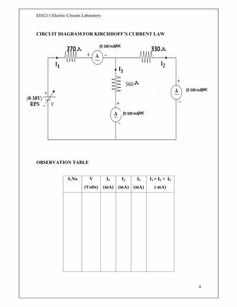
CIRCUIT DIAGRAM FOR KIRCHHOFF’S CURRENT LAW
OBSERVATION TABLE
S.No V
(Volts)
I1
(mA)
I2
(mA)
I3
(mA)
I1 = I2 + I3
( mA)

EE6211-Electric Circuits Laboratory
5
EXP.NO:
DATE:
SIMULATION AND EXPERIMENTAL VERIFICATION OF ELECTRICAL
CIRCUIT PROBLEMS USING KIRCHHOFF’S VOLTAGE AND CURRENT LAWS
AIM:
To verify (i) Kirchhoff’s current law (ii) Kirchhoff’s voltage law
APPARATUS REQUIRED:
S.No Name of the apparatus Range Type Quantity
1 RPS
2 Resistor
3 Ammeter
4 Voltmeter
5 Bread board
6 Connecting wires
SOFTWARE REQUIRED:
Matlab 7.1
KIRCHHOFF’S CURRENT LAW:
THEORY:
The law states, “The sum of the currents entering a node is equal to sum of
the currents leaving the same node”. Alternatively, the algebraic sum of currents
at a node is equal to zero.
EE6211-Electric Circuits Laboratory
6
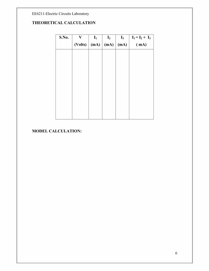
THEORETICAL CALCULATION
MODEL CALCULATION:
S.No. V
(Volts)
I1
(mA)
I2
(mA)
I3
(mA)
I1 = I2 + I3
( mA)

EE6211-Electric Circuits Laboratory
7
The term node means a common point where the different elements are connected.
Assume negative sign for leaving current and positive sign for entering current.
PROCEDURE:
1. Connect the circuit as per the circuit diagram.
2. Switch on the supply.
3. Set different values of voltages in the RPS.
4. Measure the corresponding values of branch currents I1, I2 and I3.
5. Enter the readings in the tabular column.
6. Find the theoretical values and compare with the practical values
FORMULA:
∑ Currents entering a node = ∑ Currents leaving the node
I1 = I2 + I3

EE6211-Electric Circuits Laboratory
8
CIRCUIT DIAGRAM FOR KIRCHHOFF’S VOLTAGE LAW:
OBSERVATION TABLE:
S.No. V
Volts
V1
Volts
V2
Volts
V3
Volts
V =V1+ V2
+V3
Volts

EE6211-Electric Circuits Laboratory
9
KIRCHHOFF’S VOLTAGE LAW:
THEORY:
The law states, “The algebraic sum of the voltages in a closed circuit/mesh is
zero”.
The voltage rise is taken as positive and the voltage drop is taken as negative.
PROCEDURE:
1. Connect the circuit as per the circuit diagram.
2. Switch on the supply.
3. Set different values of voltages in the RPS.
4. Measure the corresponding values of voltages (V1, V2 and V3) across resistors R1,
R2 and R3 respectively.
5. Enter the readings in the tabular column.
6. Find the theoretical values and compare with the practical values.
FORMULA:
∑ Voltages in a closed loop = 0
V-V1-V2-V3 = 0

EE6211-Electric Circuits Laboratory
10
THEORETICAL CALCULATION:
MODEL CALCULATION:
S.No. V
Volts
V1
Volts
V2
Volts
V2
Volts
V =V1+ V2 + V3
Volts

EE6211-Electric Circuits Laboratory
11
SIMULATION PROCEDURE:
1. Open a new MATLAB/SIMULINK model
2. Connect the circuit as shown in the figure
3. Debug and run the circuit
4. For different input voltages, record the current and voltages and verify with
theoretical values.
EE6211-Electric Circuits Laboratory
12
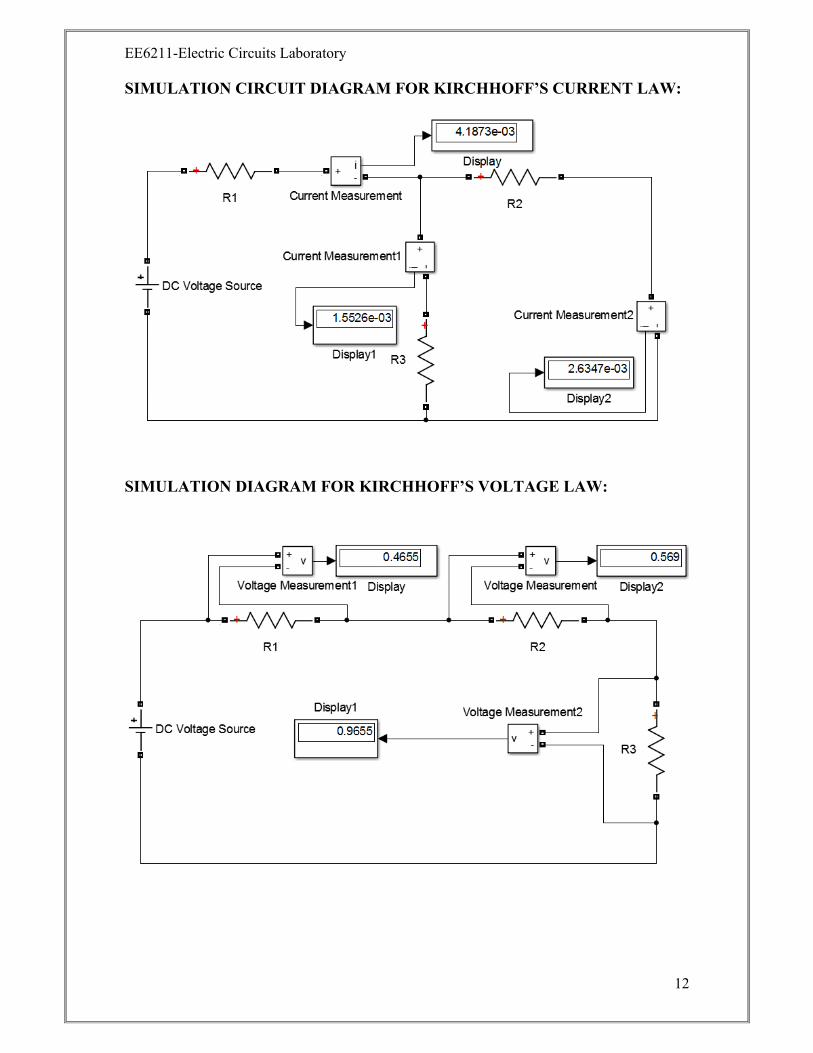
SIMULATION CIRCUIT DIAGRAM FOR KIRCHHOFF’S CURRENT LAW:
SIMULATION DIAGRAM FOR KIRCHHOFF’S VOLTAGE LAW:

EE6211-Electric Circuits Laboratory
13
VIVA QUESTIONS:
1. State Kirchhoff’s Voltage Law.
2. State Kirchhoff’s Current Law.
3. What is current division rule?
4. What is voltage division rule?
5. Give the equivalent resistance when ‘n’ number of resistances is connected in
series.
6. Give the equivalent resistance when ‘n’ number of resistances is connected in
parallel
RESULT:
Thus the Kirchhoff’s Current and Voltage laws are verified.

EE6211-Electric Circuits Laboratory
14
CIRCUIT DIAGRAM FOR THEVENIN’S THEOREM:
TO FIND LOAD CURRENT:

EE6211-Electric Circuits Laboratory
15
EXP.NO:
DATE:
SIMULATION AND EXPERIMENTAL VERIFICATION OF ELECTRICAL
CIRCUIT PROBLEMS USING THEVENIN’S THEOREM
AIM:
To verify Thevenin’s theorem.
APPARATUS REQUIRED:
S.No no Name of the Components /
Equipment
Type/Range Quantity required
1 Resistor
2 Dc power supply
3 Voltmeter
4 Ammeter
5 Wires
6 Bread board
SOFTWARE REQUIRED:
Matlab 7.1

EE6211-Electric Circuits Laboratory
16
TO FIND Vth:
TO FIND Rth:
EE6211-Electric Circuits Laboratory
17
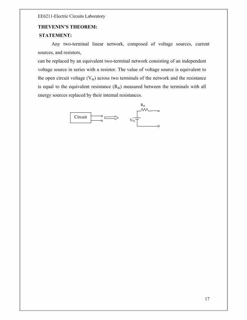
THEVENIN’S THEOREM:
STATEMENT:
Any two-terminal linear network, composed of voltage sources, current
sources, and resistors,
can be replaced by an equivalent two-terminal network consisting of an independent
voltage source in series with a resistor. The value of voltage source is equivalent to
the open circuit voltage (Vth) across two terminals of the network and the resistance
is equal to the equivalent resistance (Rth) measured between the terminals with all
energy sources replaced by their internal resistances.
Circuit
Rth
Vth

EE6211-Electric Circuits Laboratory
18
THEVENIN’S EQUIVALENT CIRCUIT
OBSERVATION TABLE
S.
No
Vdc
Vth
(Volts) Rth
( Ω )
Current through
Load Resistance
IL(mA)
Practical
Value
Theoretical
Value
Practical
Value
Theoretical
Value
Practical
Value
Theoretical
Value

EE6211-Electric Circuits Laboratory
19
PROCEDURE:
1. Give connections as per the circuit diagram.
2. Measure the current through RL in the ammeter.
3. Open circuit the output terminals by disconnecting load resistance RL.
4. Connect a voltmeter across AB and measure the open circuit voltage Vth.
5. To find Rth, replace the voltage source by short circuit.
6. Give connections as per the Thevenin’s Equivalent circuit.
7. Measure the current through load resistance in Thevenin’s Equivalent circuit.
8. Verify Thevenin’s theorem by comparing the measured currents in Thevenin’s
Equivalent circuit with the values calculated theoretically.
SIMULATION PROCEDURE:
1. Open a new MATLAB/SIMULINK model
2. Connect the circuit as shown in the figure
3. Debug and run the circuit
4. For different input voltages, record the current and voltages and verify with
theoretical values.

EE6211-Electric Circuits Laboratory
20
SIMULATION:
TO FIND LOAD CURRENT:
TO FIND Vth:
THEVENIN’S EQUIVALENT CIRCUIT:
EE6211-Electric Circuits Laboratory
21
VIVA QUESTIONS:
1. What is meant by a linear network?
2. State Thevenin’s Theorem.
3. How do you calculate thevenin’s resistance?
RESULT:
Thus the Thevenin’s theorem was verified.
EE6211-Electric Circuits Laboratory
22
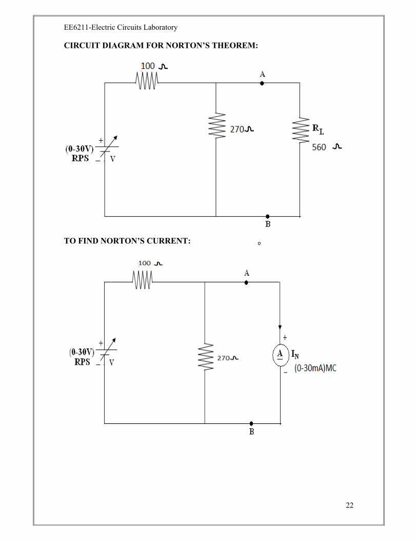
CIRCUIT DIAGRAM FOR NORTON’S THEOREM:
TO FIND NORTON’S CURRENT:

EE6211-Electric Circuits Laboratory
23
EXP.NO:
DATE:
SIMULATION AND EXPERIMENTAL VERIFICATION OF ELECTRICAL
CIRCUIT PROBLEMS USING NORTON’S THEOREM
AIM:
To verify Norton’s theorem.
APPARATUS REQUIRED:
S.No no Name of the Components /
Equipment
Type/Range Quantity required
1 Resistor
2 Dc power supply
3 Voltmeter
4 Ammeter
5 Wires
6 Bread board
SOFTWARE REQUIRED:
Matlab 7.1
NORTON’S THEOREM
STATEMENT:
Any two-terminal linear network, composed of voltage sources, current
sources, and resistors, can be replaced by an equivalent two-terminal network
consisting of an independent current source in parallel with a resistor. The value of the
current source is the short circuit current (IN) between the two terminals of the
network and the resistance is equal to the equivalent resistance (RN) measured
between the terminals with all energy sources replaced by their internal resistances.
EE6211-Electric Circuits Laboratory
24
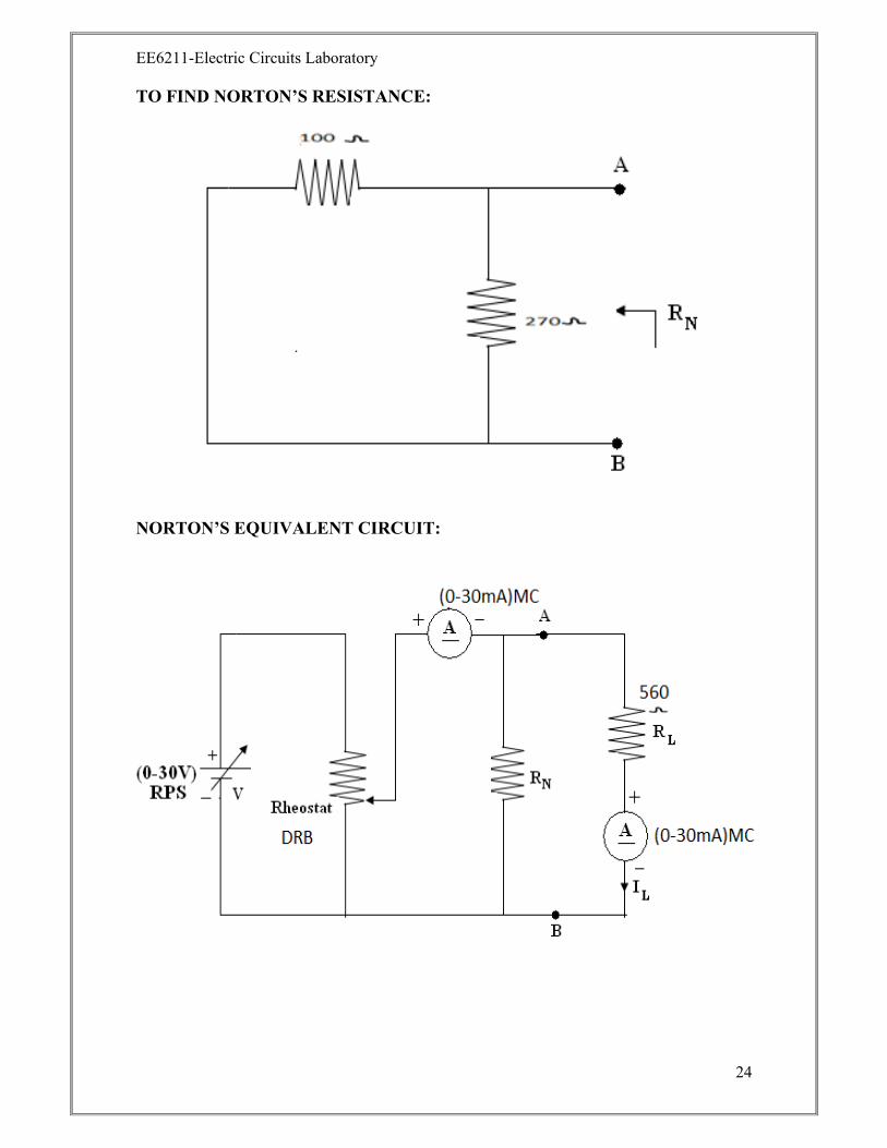
TO FIND NORTON’S RESISTANCE:
NORTON’S EQUIVALENT CIRCUIT:

EE6211-Electric Circuits Laboratory
25
PROCEDURE:
1. Give connections as per the circuit diagram.
2. Measure the current through RL in ammeter.
3. Short circuit A and B through an ammeter.
4. Measure the Norton current in the ammeter.
5. Find out the Norton’s Resistance viewed from the output terminals.
6. Give connections as per the Norton’s Equivalent circuit.
7. Measure the current through RL.
8. Verify Norton’s theorem by comparing currents in RL directly and that
obtained with the equivalent circuit.
SIMULATION PROCEDURE:
1. Open a new MATLAB/SIMULINK model
2. Connect the circuit as shown in the figure
3. Debug and run the circuit
4. For different input voltages, record the current and voltages and verify with
theoretical values.
Circuit RN IN

EE6211-Electric Circuits Laboratory
26
TO FIND LOAD CURRENT:
TO FIND NORTON’S CURRENT:
EE6211-Electric Circuits Laboratory
27
VIVA QUESTIONS:
1. How do you calculate Norton’s resistance?
2. State Norton’s Theorem.
3. Give the usefulness of Norton’s theorems.
RESULT:
Thus the Norton’s theorem was verified.

EE6211-Electric Circuits Laboratory
28
CIRCUIT DIAGRAM FOR SUPERPOSITION THEOREM:
CIRCUIT DIAGRAM WITH V1 ACTING INDEPENDENTLY:

EE6211-Electric Circuits Laboratory
29
EXP.NO:
DATE:
SIMULATION AND EXPERIMENTAL VERIFICATION OF ELECTRICAL
CIRCUIT PROBLEMS USING SUPERPOSITION THEOREM
AIM:
To verify superposition theorem.
APPARATUS REQUIRED:
S.No Name of the Components /
Equipment Type/Range Quantity required
1 Resistor
2 Dc power supply
3 Voltmeter
4 Ammeter
5 Wires
6 Bread board
SOFTWARE REQUIRED:
Matlab 7.1
SUPERPOSITION THEOREM:
STATEMENT:
In any linear, bilateral network energized by two or more sources, the
total response is equal to the algebraic sum of the responses caused by
individual sources acting alone while the other sources are replaced by their
internal resistances.
To replace the other sources by their internal resistances, the voltage
sources are short- circuited and the current sources open- circuited.

EE6211-Electric Circuits Laboratory
30
CIRCUIT DIAGRAM WITH V2 ACTING INDEPENDENTLY:
OBSERVATION TABLE:
Experimental Values: Theoretical Values:
V1
(Volts)
V2
(Volts)
I3
(mA)
V1
(Volts)
V2
(Volts)
I3
(mA)

EE6211-Electric Circuits Laboratory
31
FORMULAE :
I3’ + I3
’’ = I3
PROCEDURE :
1. Connections are made as per the circuit diagram given in Fig. 1.
2. Switch on the supply.
3. Note the readings of three Ammeters.
4. One of the voltage source V1 is connected and the other voltage source V2 is
short circuited as given in Fig.2.
5. Note the three ammeter readings.
6. Now short circuit the voltage source V1 and connect the voltage source V2 as
given in the circuit diagram of Fig. 3.
7. Note the three ammeter readings.
8. Algebraically add the currents in steps (5) and (7) above to compare with the
current in step (3) to verify the theorem.
9. Verify with theoretical values.
EE6211-Electric Circuits Laboratory
32
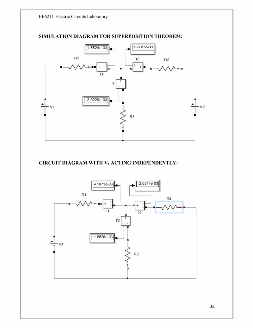
SIMULATION DIAGRAM FOR SUPERPOSITION THEOREM:
CIRCUIT DIAGRAM WITH V1 ACTING INDEPENDENTLY:

EE6211-Electric Circuits Laboratory
33
SIMULATION PROCEDURE:
1. Open a new MATLAB/SIMULINK model
2. Connect the circuit as shown in the figure
3. Debug and run the circuit
4. For different input voltages, record the current and voltages and verify with
theoretical values.

EE6211-Electric Circuits Laboratory
34
CIRCUIT DIAGRAM WITH V2 ACTING INDEPENDENTLY:
VERIFICATION OF SUPERPOSITION THEOREM:
Practical:
S.No. I3
(mA)
I3’
(mA)
I3’’
(mA)
I3= I3’ +I3’’
(mA)

EE6211-Electric Circuits Laboratory
35
Theoretical:
S.No. I3
(mA)
I3’
(mA)
I3’’
(mA)
I3= I3’ +I3’’
(mA)
VIVA QUESTIONS:
1. State Superposition Theorem.
2. What is meant by a linear system?
3. Give the usefulness of Superposition Theorem.
4. How will you apply Superposition Theorem to a linear circuit containing
both dependent and independent sources?
5. State the limitations of Superposition theorem.
RESULT:
Thus the Superposition theorem was verified.

EE6211-Electric Circuits Laboratory
36
CIRCUIT DIAGRAM FOR MAXIMUM POWER TRANSFER THEOREM:
OBSERVATION TABLE:
S.No. RL (kΩ) IL (mA) P = I2RL (mW)
Practical
Value
Theoretical
Value
Practical
Value
Theoretical
Value
EE6211-Electric Circuits Laboratory
37
EXP.NO:
DATE:
SIMULATION AND EXPERIMENTAL VERIFICATION OF ELECTRICAL
CIRCUIT PROBLEMS USING MAXIMUM POWER TRANSFER THEOREM
AIM:
To verify maximum power transfer theorem.
APPARATUS REQUIRED:
S.No Name of the Components /
Equipment Type/Range Quantity required
1 Resistor
2 Dc power supply
3 Voltmeter
4 Ammeter
5 Wires
6 Bread board
SOFTWARE REQUIRED:
Matlab 7.1
MAXIMUM POWER TRANSFER THEOREM:
THEORY:
The Maximum Power Transfer Theorem states that maximum power is
delivered from a source to a load when the load resistance is equal to source
resistance.

EE6211-Electric Circuits Laboratory
38
SIMULATION DIAGRAM FOR MAXIMUM POWER TRANSFER
THEOREM:
MODEL GRAPH:
MODEL CALCULATION:

EE6211-Electric Circuits Laboratory
39
PROCEDURE:
1. Find the Load current for the minimum position of the Rheostat theoretically.
2. Select the ammeter Range.
3. Give connections as per the circuit diagram.
4. Measure the load current by gradually increasing RL .
5. Enter the readings in the tabular column.
6. Calculate the power delivered in RL.
7. Plot the curve between RL and power.
8. Check whether the power is maximum at a value of load resistance that equals
source resistance.
9. Verify the maximum power transfer theorem.
SIMULATION PROCEDURE:
1. Open a new MATLAB/SIMULINK model
2. Connect the circuit as shown in the figure
3. Debug and run the circuit
4. For different input voltages, record the current and voltages and verify with
theoretical values.
VIVA QUESTIONS:
1. Define Power. What is the unit of Power?
2. State Maximum Power Transfer Theorem
RESULT:
Thus the Maximum power transfer theorem was verified.
EE6211-Electric Circuits Laboratory
40
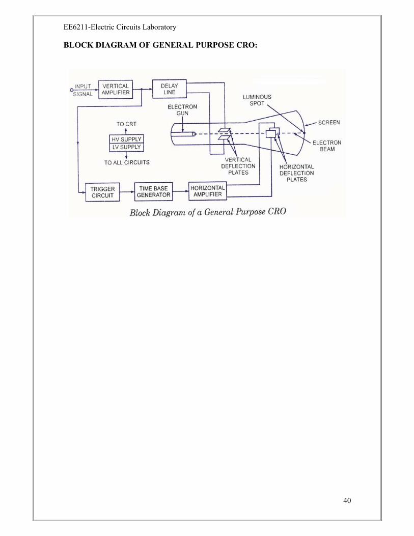
BLOCK DIAGRAM OF GENERAL PURPOSE CRO:

EE6211-Electric Circuits Laboratory
41
EXP NO.:
DATE:
STUDY OF ANALOG AND DIGITAL OSCILLOSCOPES AND
MEASUREMENT OF SINUSOIDAL VOLTAGE, FREQUENCY AND POWER
FACTOR
AIM:
The aim of the experiment is to understand the operation of cathode ray
oscilloscope (CRO) and to become familiar with its usage, also to perform an
experiment using function generator to measure amplitude, time period, frequency &
power factor of the time varying signals using a calibrated cathode ray oscilloscope.
APPARATUS REQUIRED:
THEORY:
The cathode ray oscilloscope (CRO) provides a visual presentation of any
waveform applied to the input terminal. The oscilloscope consists of the
following major subsystems.
• Cathode ray tube (CRT)
• Vertical amplifier
• Horizontal amplifier
• Sweep Generator
• Trigger circuit
• Associated power supply
It can be employed to measure quantities such as peak voltage, frequency,
phase difference, pulse width, delay time, rise time, and fall time.
S.No Name of the Components/Equipment Qty
1. CRO 1
2. Function generator 2
3. Probes 2

EE6211-Electric Circuits Laboratory
42
S.No Type of
wave
Time
period (T)
Amplitude Theoretical
Frequency
Practical
Frequency
1.
2.
3.

EE6211-Electric Circuits Laboratory
43
CATHODE RAY TUBE:
The CRT is the heart of the CRO providing visual display of an input signal
waveform. A CRT contains four basic parts:
• An electron gun to provide a stream of electrons.
• Focusing and accelerating elements to produce a well define beam of
electrons.
• Horizontal and vertical deflecting plates to control the path of the
electron beam.
• An evacuated glass envelope with a phosphorescent which glows visibly
when struck by electron beam.
A Cathode containing an oxide coating is heated indirectly by a filament resulting
in the release of electrons from the cathode surface. The control grid which has a
negative potential, controls the electron flow from the cathode and thus control the
number of electron directed to the screen. Once the electron passes the control grid,
they are focused into a tight beam and accelerated to a higher velocity by focusing and
accelerating anodes. The high velocity and well defined electron beam then passed
through two sets of deflection plates.
The First set of plates is oriented to deflect the electron beam vertically. The angle
of the vertical deflection is determined by the voltage polarity applied to the deflection
plates. The electron beam is also being deflected horizontally by a voltage applied to
the horizontal deflection plates. The tube sensitivity to deflecting voltages can be
expressed in two ways that are deflection factor and deflection sensitivity.
The deflected beam is then further accelerated by very high voltages applied to the
tube with the beam finally striking a phosphorescent material on the inside face of the
tube. The phosphor glows when struck by the energetic electrons.
CONTROL GRID:
Regulates the number of electrons that reach the anode and hence the
brightness of the spot on the screen.

EE6211-Electric Circuits Laboratory
44

EE6211-Electric Circuits Laboratory
45
FOCUSING ANODE:
Ensures that electrons leaving the cathode in slightly different directions are
focused down to a narrow beam and all arrive at the same spot on the screen.
ELECTOR GUN:
Cathode, control grid, focusing anode, and accelerating anode.
DEFLECTING PLATES:
Electric fields between the first pair of plates deflect the electrons horizontally
and an electric field between the second pair deflects them vertically. If no deflecting
fields are present, the electrons travel in a straight line from the hole in the
accelerating anode to the center of the screen, where they produce a bright spot. In
general purpose oscilloscope, amplifier circuits are needed to increase the input signal
to the voltage level required to operate the tube because the signals measured using
CRO are typically small. There are amplifier sections for both vertical and horizontal
deflection of the beam.
VERTICAL AMPLIFIER:
Amplify the signal at its input prior to the signal being applied to the vertical
deflection plates.
HORIZONTAL AMPLIFIER:
Amplify the signal at its input prior to the signal being applied to the horizontal
deflection plates.
SWEEP GENERATOR:
Develop a voltage at the horizontal deflection plate that increases linearly with
time.
OPERATION:
The four main parts of the oscilloscope CRT are designed to create and direct
an electron beam to a screen to form an image. The oscilloscope links to a circuit that
directly connects to the vertical deflection plates while the horizontal plates have
linearly increasing charge to form a plot of the circuit voltage over time. In an
operating cycle, the heater gives electrons in the cathode enough energy to escape.
The electrons are attracted to the accelerating anode and pulled through a control grid
that regulates the number of electrons in the beam, a focusing anode that controls the

EE6211-Electric Circuits Laboratory
46

EE6211-Electric Circuits Laboratory
47
width of the beam, and the accelerating anode itself. The vertical and horizontal
deflection plates create electric field that bend the beam of electrons. The electrons
finally hit the fluorescent screen which absorbs the energy from the electron beam and
emits it in the form of light to display an image at the end of the glass tube.
PRECAUTIONS:
1. Do not leave a ‘bright spot’ on the screen for any length of time.
2. Do not apply signals that exceed the scopes voltage rating.
3. Do not try make accurate measurements on signals whose frequency is outside
the scope’s frequency specifications.
4. Be aware that the scope’s input circuitry can cause loading effects on the
circuitry under test-use correct probe for the work.
PRODEDURE:
1. Measurement of Voltage Using CRO : A voltage can be measured by noting
the Y deflection produced by the voltage; using this deflection in conjunction with the
Y-gain setting, the voltage can be calculated as follows : V = ( no. of boxes in cm. ) x
( selected Volts/cm scale )
2 .Measurement of Current and Resistance Using a CRO: Using the general
method, a correctly calibrated CRO can be used in conjunction with a known value of
resistance R to determine the current I flowing through the resistor.
3 Measurement of Frequency Using a CRO: A simple method of determining
the frequency of a signal is to estimate its periodic time from the trace on the screen of
a CRT. However this method has limited accuracy, and should only be used where
other methods are not available. To calculate the frequency of the observed signal, one
has to measure the period, i.e. the time taken for 1 complete cycle, using the calibrated
sweep scale. The period could be calculated by T = (no. of squares in cm) x (selected
Time/cm scale) Once the period T is known, the frequency is given by f (Hz)=
1/T(sec)

EE6211-Electric Circuits Laboratory
48

EE6211-Electric Circuits Laboratory
49
4. Measurement of Phase: The calibrated time scales can be used to calculate
the phase shift between two sinusoidal signals of the same frequency. If a dual trace or
beam CRO is available to display the two signals simultaneously (one of the signals is
used for synchronization), both of the signals will appear in proper time perspective
and the amount of time difference between the waveforms can be measured. This, in
turn can be utilized to calculate the phase angle θ, between the two signals.
Referring to the fig below the phase shift can be calculated by the formula;
θ°=
MEASUREMENT OF PF:
The power factor is calculated by the formula
pf=VICOS θ.
VIVA QUESTIONS:
1. What is a CRO?
2. How can we measure the voltage using a CRO?
3. Explain the different parts of the CRO
4. Explain the operation of a CRO.
RESULT:
Thus the Analog and digital oscilloscopes were studied and measurement
of sinusoidal voltage, frequency and power factor was done.

EE6211-Electric Circuits Laboratory
50
CIRCUIT DIAGRAM FOR RC TRANSIENT:
MODEL GRAPH:

EE6211-Electric Circuits Laboratory
51
EXP NO. :
DATE :
SIMULATION AND EXPERIMENTAL VALIDATION OF R-C ELECTRIC
CIRCUIT TRANSIENTS
AIM:
To find the time constant of series R-C electric circuits
SOFTWARE REQUIRED:
PSpice Lite
APPARATUS REQUIRED:
S.No. Name of the
Components/Equipment
Range/Type Quantity
required
1 Resistor 100 Ώ 1
2 Function generator - 1
3 Voltmeter (0-30)V MI 1
4 Decade capacitance box - 1
5 Wires Single strand Few nos
6 Bread board 1
THEORY:
RC CIRCUIT:
Consider a series RC circuit as shown. The switch is in open state initially.
There is no charge on condenser and no voltage across it. At instant t=0, switch is
closed.
Immediately after closing a switch, the capacitor acts as a short circuit, so
current at the time of switching is high. The voltage across capacitor is zero at t= 0+ as
capacitor acts as a short circuit, and the current is maximum given by,
i = V/R Amps

EE6211-Electric Circuits Laboratory
52
OBSERVATION TABLE:
S.No. Frequency
(Hz)
Time
(s)
Voltage across the
capacitor VC
(v)
MODEL CALCULATION:

EE6211-Electric Circuits Laboratory
53
RCt
inC e
RVI
−
= )1( RCt
inC eVV−
−=
)1( 1−−= eVV inC
This current is maximum at t=0+ which is charging current. As the capacitor starts
charging, the voltage across capacitor VC starts increasing and charging current starts
decreasing. After some time, when the capacitor charges to V volts, it achieves steady
state. In steady state it acts as an open circuit and current will be zero finally.
Charging current and voltage in capacitor are given as below,
The term RC in equation of VC or IC is called Time constant and denoted by τ,
measured in seconds.
When, t = RC = τ then,
VC = 0.632Vin
So time constant of series RC circuit is defined as time required by the
capacitor voltage to rise from zero to 0.632 of its final steady state value during
charging.
Thus, time constant of RC circuit can be defined as time seconds, during which
voltage across capacitor (stating from zero) would reach its final steady state value if
its rate of change was maintained constant at its initial value throughout charging
period.
PROCEDURE:
1. Make the connections as per the circuit diagram.
2. Vary the frequency by using function generator.
3. For different frequencies tabulate the value of voltage across the capacitor .
4. Calculate the time period.
5. Plot the graph for time period Vs voltage across the capacitor.

EE6211-Electric Circuits Laboratory
54
SIMULATION DIAGRAM:
EE6211-Electric Circuits Laboratory
55
SIMULATION PROCEDURE:
1. Open a new PSpice CAPTURE project.
2. Connect the circuit as shown in the figure.
3. Create simulation profile and run the model
VIVA QUESTIONS:
1. Differentiate steady state and transient state.
2. What is meant by transient response?
3. Define the time constant of a RL Circuit.
4. Define the time constant of a RC Circuit.
5. What is meant by forced response?
RESULT:
Thus the transient responses of RC circuit are found practically.

EE6211-Electric Circuits Laboratory
56
SIMULATION CIRCUIT DIAGRAM:
OUTPUT WAVEFORM: Case (i):

EE6211-Electric Circuits Laboratory
57
EXP NO.: DATE :
SIMULATION AND EXPERIMENTAL VALIDATION OF FREQUENCY
RESPONSE OF RLC ELECTRIC CIRCUIT
AIM:
To simulate and find the frequency response of RLC electric circuits. SOFTWARE REQUIRED:
PSpice Lite
APPARATUS REQUIRED:
S.No. Name of the Components/Equipment
Range/Type Quantity required
1 Resistor 1000 Ώ 1 2 Function generator - 1 3 Voltmeter (0-30)V MI 1 4 Decade capacitance box - 1 5 Decade Inductance box - 1 6 Wires Single strand Few nos 7 Bread board 1
THEORY:
RLC CIRCUIT: Consider a series RLC circuit as shown. The switch is in open state initially.
There is no charge on condenser and no voltage across it. At instant t=0, switch is
closed.
Immediately after closing a switch, the capacitor acts as a short circuit, so
current at the time of switching is high. The voltage across capacitor is zero at t= 0+ as
capacitor acts as a short circuit, and the current is maximum given by,
i = V/R Amps

EE6211-Electric Circuits Laboratory
58
OBSERVATION TABLE:
S.No. Frequency (Hz)
Time (s)
Voltage across the capacitor VC
(v)
MODEL CALCULATION:

EE6211-Electric Circuits Laboratory
59
This current is maximum at t=0+ which is charging current. As the capacitor starts
charging, the voltage across capacitor VC starts increasing and charging current starts
decreasing. After some time, when the capacitor charges to V volts, it achieves steady
state. In steady state it acts as an open circuit and current will be zero finally.
Laplace transform of current flowing through the circuit is,
2
V/LI(s)= R 1s + s+L LC
Case (i):
If 2
2RL
⎡ ⎤⎢ ⎥⎣ ⎦
> 1LC
The roots are real and distinct. The current is over damped. Case (ii):
If 2
2RL
⎡ ⎤⎢ ⎥⎣ ⎦
= 1LC
The roots are equal. The current is critically damped. Case (iii):
If 2
2RL
⎡ ⎤⎢ ⎥⎣ ⎦
< 1LC
The roots become complex conjugate. The current is oscillatory in nature. PROCEDURE:
1. Make the connections as per the circuit diagram
2. Vary the frequency by using function generator
3. For different frequencies tabulate the value of voltage across the capacitor
4. Calculate the time period
5. Plot the graph for time period Vs voltage across the capacitor.

EE6211-Electric Circuits Laboratory
60
Case (ii):
Case (iii):

EE6211-Electric Circuits Laboratory
61
SIMULATION PROCEDURE:
4. Open a new PSpice CAPTURE project.
5. Connect the circuit as shown in the figure.
6. Create simulation profile and run the model
VIVA QUESTIONS
1. What is meant by transient response?
2. Define the time constant of a RL Circuit.
3. Define the time constant of a RC Circuit.
4. What is meant by forced response?
RESULT: Thus the transient responses of RLC circuit are found practically.

EE6211-Electric Circuits Laboratory
62
CIRCUIT DIAGRAM FOR SERIES RESONANCE:
OBSERVATION TABLE:
MODEL CALCULATION:
S.No. Frequency in Hz Output Current in mA

EE6211-Electric Circuits Laboratory
63
EXP NO.:
DATE :
DESIGN AND SIMULATION OF SERIES RESONANCE CIRCUIT
AIM:
To plot the current Vs frequencies graph of series resonant circuits and hence
measure their bandwidth, resonant frequency and Q factor.
SOFTWARE REQUIRED:
PSpice 9.1 Lite
APPARATUS REQUIRED:
S.No. Name of the
Components/Equipment
Type Range Quantity
required
1 Function Generator - - 1
2 Resistor - 100 Ω 1
3 Decade Inductance Box - - 1
4 Decade Capacitance Box - - 1
5 Ammeter MI (0-30) mA 1
6 Connecting Wires Single
strand
- Few nos
THEORY:
A circuit is said to be in resonance when applied voltage V and current I
are in phase with each other. Thus at resonance condition, the equivalent complex
impedance of the circuit consists of only resistance (R) and hence current is
maximum. Since V and I are in phase, the power factor is unity.
The complex impedance
Z = R + j (XL – XC)
Where XL = ωL

EE6211-Electric Circuits Laboratory
64
PSpice SIMULATION:
OUTPUT WAVWFORM:
MATLAB SIMULATION:

EE6211-Electric Circuits Laboratory
65
XC = 1/ωC
At resonance, XL= XC and hence Z= R
BANDWIDTH OF A RESONANCE CIRCUIT:
Bandwidth of a circuit is given by the band of frequencies which lies between
two points on either side of resonance frequency, where current falls through 1/1.414
of the maximum value of resonance. Narrow is the bandwidth, higher the selectivity
of the circuit.
As shown in the model graph, the bandwidth AB is given by f2 – f1. f1 is the
lower cut off frequency and f2 is the upper cut off frequency.
Q - FACTOR:
In the case of a RLC series circuit, Q-factor is defined as the voltage
magnification in the circuit at resonance. At resonance, current is maximum. Io= V/R.
The applied voltage V = IoR
Voltage magnification = VL/V = IoXL
In the case of resonance, high Q factor means not only high voltage, but also higher
sensitivity of tuning circuit. Q factor can be increased by having a coil of large
inductance, not of smaller ohmic resistance.
Q = ωL / R
FORMULAE USED:
Resonant frequency fr = LCπ2
1 Hz
Bandwidth BW = f2 – f1
Quality Factor = BWfr
PROCEDURE:
1. Connect the circuit as per the circuit diagram.
2. Vary the frequency and note down the corresponding meter reading.
3. Draw the current Vs frequency curve and measure the bandwidth, resonant
frequency and Q factor.

EE6211-Electric Circuits Laboratory
66
MODEL GRAPH FOR SERIES RESONANCE
Imax
0.707Imax
PLOT OF MAGNITUDE & PHASE ANGLE OF CURRENT FOR VARIOUS
FREQUENCIES:
Current in mA
f1 fr f2
A B
Frequency in Hz

EE6211-Electric Circuits Laboratory
67
SIMULATION PROCEDURE:
1. Open a new MATLAB/SIMULINK model or PSpice CAPTURE project.
2. Connect the circuit as shown in the figure.
3. Debug and run the circuit.
4. By double clicking the power gui plot the value of current for the different
values of frequencies (for MATLAB Simulink).
5. For PSpice CAPTURE run the model create simulation profile and run the
model.
VIVA QUESTIONS:
1. Define Bandwidth.
2. Define Quality factor.
3. What is meant by selectivity?
4. Give the significance of Q- factor.
5. What is meant by resonance?
6. What are the characteristics of a series resonant circuit?
7. What will be the power factor of the circuit at resonance?
RESULT:
Thus the current Vs frequency graphs of series and parallel resonant circuits
were plotted and the bandwidth, resonant frequency and Q factor were measured.
They were found to be
(a) Series resonance
Resonant frequency = ____________
Bandwidth = ____________
Q- Factor = ____________

EE6211-Electric Circuits Laboratory
68
CIRCUIT DIAGRAM FOR PARALLEL RESONANCE:
OBSERVATION TABLE:
S.No. Frequency in Output
MODEL GRAPH FOR PARALLEL RESONANCE:
Frequency in Hz
Imin
fr
Cur
rent
in m
A

EE6211-Electric Circuits Laboratory
69
EXP NO. :
DATE :
DESIGN AND SIMULATION OF PARALLEL RESONANT CIRCUITS
AIM:
To plot the magnitude & phase angle of current for various frequencies for the
given RLC parallel circuit.
SOFTWARE REQUIRED:
Matlab 7.1 or PSpice 9.1 Lite
APPARATUS REQUIRED:
S.No. Name of the Components/Equipment
Type Range Quantity required
1 Function Generator - - 1 2 Resistor - 100 Ω 1 3 Decade Inductance Box - - 1 4 Decade Capacitance Box - - 1 5 Ammeter MI (0-30) mA 1 6 Connecting Wires Single
strand - Few nos
THEORY:
A circuit is said to be in resonance when applied voltage V and current I are in
phase with each other. Thus at resonance condition, the equivalent complex
impedance of the circuit consists of only resistance (R) and hence current is
maximum. Since V and I are in phase, the power factor is unity.
The complex impedance
Z = R + j (XL – XC)
Where XL = ωL
XC = 1/ωC
At resonance, XL= XC and hence Z= R

EE6211-Electric Circuits Laboratory
70
PSpice SIMULATION:
OUTPUT WAVEFORM:

EE6211-Electric Circuits Laboratory
71
BANDWIDTH OF A RESONANCE CIRCUIT:
Bandwidth of a circuit is given by the band of frequencies which lies between
two points on either side of resonance frequency, where current falls through 1/1.414
of the maximum value of resonance. Narrow is the bandwidth, higher the selectivity
of the circuit. As shown in the model graph, the bandwidth AB is given by f2 – f1. f1 is
the lower cut off frequency and f2 is the upper cut off frequency.
Q - FACTOR:
In the case of a RLC series circuit, Q-factor is defined as the voltage
magnification in the circuit at resonance. At resonance, current is maximum. Io= V/R.
The applied voltage V = IoR
Voltage magnification = VL/V = IoXL
In the case of resonance, high Q factor means not only high voltage, but also higher
sensitivity of tuning circuit. Q factor can be increased by having a coil of large
inductance, not of smaller ohmic resistance.
Q = ωL / R
FORMULAE USED:
Resonant frequency fr = LCπ2
1 Hz
Bandwidth BW = f2 – f1
Quality Factor = BWfr
PROCEDURE:
1. Connect the circuit as per the circuit diagram.
2. Vary the frequency and note down the corresponding meter reading.
3. Draw the current Vs frequency curve and measure the bandwidth, resonant
frequency and Q factor.
.

EE6211-Electric Circuits Laboratory
72
MATLAB SIMULATION:
PLOT OF MAGNITUDE & PHASE ANGLE OF CURRENT FOR VARIOUS
FREQUENCIES:

EE6211-Electric Circuits Laboratory
73
SIMULATION PROCEDURE:
1. Open a new MATLAB/SIMULINK model or PSpice CAPTURE project.
2. Connect the circuit as shown in the figure.
3. Debug and run the circuit.
4. By double clicking the power gui plot the value of current for the different
values of frequencies (for MATLAB Simulink).
5. For PSpice CAPTURE run the model create simulation profile and run the
model
VIVA QUESTIONS:
1. Define Bandwidth.
2. Define Quality factor.
3. What is meant by selectivity?
4. Give the significance of Q- factor.
5. What is meant by resonance?
6. What are the characteristics of a parallel resonant circuit?
7. What will be the power factor of the circuit at resonance?
RESULT:
Thus the current Vs frequency graphs of series and parallel resonant circuits
were plotted and the bandwidth, resonant frequency and Q factor were measured.
They were found to be
(a) Parallel resonance
Resonant frequency = ____________
Bandwidth = ____________
Q- Factor = ____________

EE6211-Electric Circuits Laboratory
74
SIMULATTION DIAGRAM:
3 Φ BALANCED STAR CONNECTED NETWORK:

EE6211-Electric Circuits Laboratory
75
EXP NO.:
DATE :
SIMULATION OF THREE PHASE BALANCED AND UNBALANCED STAR,
DELTA NETWORKS CIRCUITS
AIM:
To simulate three phase balanced and unbalanced star, delta networks circuits.
SOFTWARE REQUIRED:
Matlab 7.1
THEORY:
BALANCED THREE- PHASE CIRCUIT:
Balanced phase voltages are equal in magnitude and are out of phase with each
other by 120°.The phase sequence is the time order in which the voltages pass through
their respective maximum values. A balanced load is one in which the phase
impedances are equal in magnitude and in phase.
POSSIBLE LOAD CONFIGURATIONS:
Four possible connections between source and load:
1. Y-Y connection (Y-connected source with a Y-connected load)
2. Y-∆ connection (Y-connected source with a ∆-connected load)
3. ∆-∆ connection
4. ∆-Y connection
UNBALANCED THREE- PHASE CIRCUIT:
An unbalanced system is due to unbalanced voltage sources or an unbalanced
load. To calculate power in an unbalanced three-phase system requires that we find
the power in each phase. The total power is not simply three times the power in one
phase but the sum of the powers in the three phases.

EE6211-Electric Circuits Laboratory
76
3 Φ UNBALANCED DELTA CONNECTED NETWORK:

EE6211-Electric Circuits Laboratory
77
VIVA QUESTIONS:
1. What do you meant by balanced circuit?
2. List the possible load configuration?
3. What is mean by unbalanced circuit?
RESULT:
Thus the three phase balanced and unbalanced star, delta network circuits were
simulated and verified.
EE6211-Electric Circuits Laboratory
78
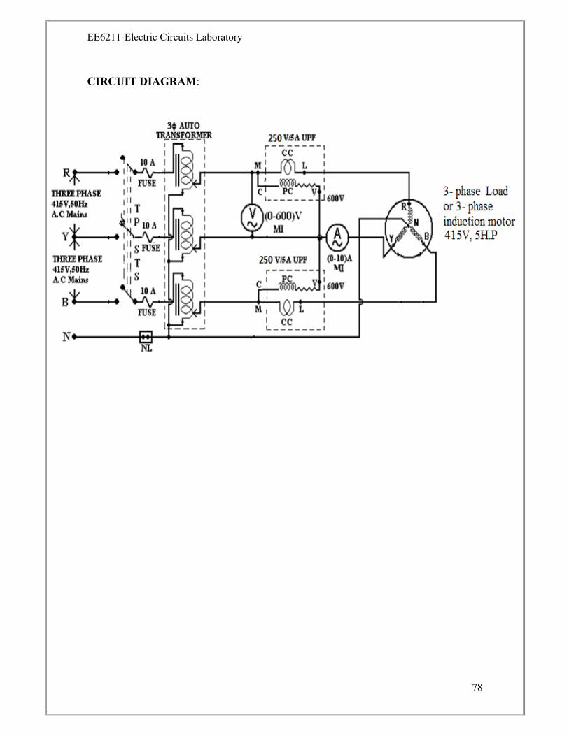
CIRCUIT DIAGRAM:

EE6211-Electric Circuits Laboratory
79
EXP NO.:
DATE :
EXPERIMENTAL DETERMINATION OF POWER IN THREE PHASE
CIRCUITS BY TWO-WATT METER METHOD
AIM:
To determine the power in three-phase balanced and unbalanced circuit using
two-watt meter method.
APPARATUS REQUIRED:
THEORY:
Two wattmeter method can be employed to measure power in a 3- phase,3 wire
star or delta connected balance or unbalanced load. In this method, the current coils of
the watt meters are connected in any two lines say R and Y and potential coil of each
watt meters is joined across the same line and third line i.e. B. Then the sum of the
power measured by two watt meters W1 and W2 is equal to the power absorbed By
the 3- phase load
PROCEDURE:
1. Connect the Voltmeter, Ammeter and Watt meters to the load through 3ф
Auto transformer as shown fig and set up the Autotransformer to Zero position.
2. Switch on the 3ф A.C. supply and adjust the autotransformer till a suitable
voltage.
SLNO NAME OF ITEM SPECIFICATION QUANTITY
1. 3-phase Auto transformer 20 Amp. 440v 50 Hz 1
2. Ammeter MI(0-10A) 1
3. Voltmeter MI(0-600V) 1
4. Wattmeter 250v, 5A 2
5. 3- phase Load or 3- phase
induction motor 415V, 5H.P 1
6 Connecting wires - Few

EE6211-Electric Circuits Laboratory
80
OBSERVATION TABLE:
S.
No
Voltmeter
reading
VL
Ammeter
reading
IL
Wattmeter reading
(watts)
Total
power
P
Reactive
power
Q
Power
factor
(V) (A)
W1
obser
ved
W1
Actu
al
W2
Obser
ved
W2
actua
l
(watts) (watts)
MODEL CALCULATION:

EE6211-Electric Circuits Laboratory
81
3. Note down the readings of watt meters, voltmeter& ammeter
4. Vary the voltage by Autotransformer and note down the Various readings.
5. Now after the observation switch off and disconnect all the Equipment or
remove the lead wire.
FORMULAE USED:
1. Total power or Real power P = √3VLILCOSф =W1actual+W2actual
2. Reactive power of load= Q=√3(W1actual-W2actual)
3. tan ф= [√3(W1actual-W2actual)]/[ W1actual+W2actual]
4. Power factor=cos ф
PRECAUTION & SOURCES OF ERROR:
1. Proper currents and voltage range must be selected before putting the
instruments in the circuit.
2. If any Wattmeter reads backward, reverse its pressure coil connection and the
reading as negative.
3. As the supply voltage Fluctuates it is not possible to observe the readings
correctly.
VIVA QUESTIONS:
1. What are the various types of wattmeter?
2. How many coils are there in wattmeter?
3. What is meant by real power?
4. What is meant by apparent power?
RESULT:
The power measured in the 3-phase circuit and there corresponding power
factors are in observation table.
EE6211-Electric Circuits Laboratory
82
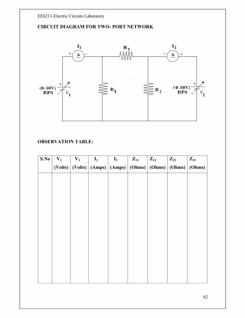
CIRCUIT DIAGRAM FOR TWO- PORT NETWORK
OBSERVATION TABLE:
S.No V1
(Volts)
V2
(Volts)
I1
(Amps)
I2
(Amps)
Z11
(Ohms)
Z12
(Ohms)
Z22
(Ohms)
Z21
(Ohms)

EE6211-Electric Circuits Laboratory
83
EXP NO.:
DATE :
DETERMINATION OF TWO PORT NETWORK PARAMETERS
AIM:
To determine the two port parameters for the given electric circuit.
APPARATUS REQUIRED:
THEORY:
1 2
1’ 2’
The terminal pair where the signal enters the network is called as the INPUT
PORT and the terminal pair where it leaves the network is called as the OUTPUT
PORT. V1& I1 are measured at the Input terminals and V2 & I2 are measured at the
Output terminals. The two port network parameters express the inter relationship
between V1, I1,V2 and I2 They are Z- parameters, Y- parameters, H-parameters, ABCD
parameters and image parameters.
S.NO Name of the
Apparatus/Component Range Type Quantity
1 Ammeter MC
2 Power Supply
3 Voltmeter MC
4 Connecting wires
5 Resistors
6 Breadboard
Linear Network

EE6211-Electric Circuits Laboratory
84
MODEL CALCULATION:

EE6211-Electric Circuits Laboratory
85
The Impedance parameters are also called as Z parameters.
V1 = Z11I1 + Z12I2 …………..……. (i)
V2 = Z21I1 + Z22I2 …………..……. (ii)
where, Z11, Z12, Z22 and Z21 are constants of the network called Z parameters.
When I2=0, (Open circuit the output terminal)
Z11=V1/I1 ….……………... (iii)
Z21=V2/I1 ..……………....... (iv)
When I1=0, ( Open circuit the Input terminal)
Z12=V1/I2 ….……………... (v)
Z22=V2/I2 ….……………... (vi)
PROCEDURE:
1. Connect the circuit as per the circuit diagram.
2. Open circuit the output terminal (2,2’).
3. Vary the power supply to a fixed value and note down the ammeter and
voltmeter readings.
4. Open circuit the Input terminal (1,1’).
5. Vary the power supply to a fixed value and note down the ammeter and
voltmeter readings.
6. Tabulate the readings and calculate the Z parameters.
VIVA QUESTIONS:
1. What is meant by a two-port network?
2. Give the use of two-port network model.
3. What are impedance parameters?
4. What are admittance parameters?
5. What are hybrid parameters?
6. What are ABCD parameters? Mention their significance.
RESULT:
Thus the two port parameters are measured for the given electric circuit.