Embed Size (px)
Citation preview
EECC550 - ShaabanEECC550 - Shaaban#1 Lec # 4 Winter 2000 12-13-2000
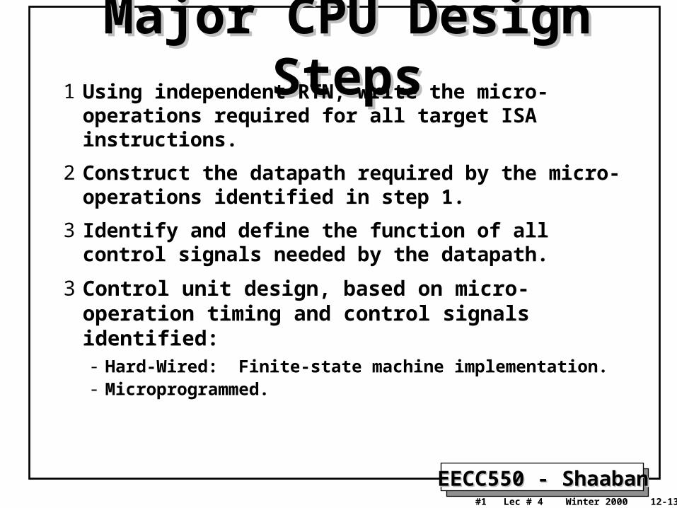
Major CPU Design StepsMajor CPU Design Steps1 Using independent RTN, write the micro-operations
required for all target ISA instructions.
2 Construct the datapath required by the micro-operations identified in step 1.
3 Identify and define the function of all control signals needed by the datapath.
3 Control unit design, based on micro-operation timing and control signals identified:- Hard-Wired: Finite-state machine implementation.- Microprogrammed.
EECC550 - ShaabanEECC550 - Shaaban#2 Lec # 4 Winter 2000 12-13-2000
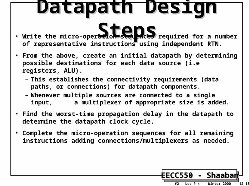
Datapath Design StepsDatapath Design Steps• Write the micro-operation sequences required for a number of
representative instructions using independent RTN.
• From the above, create an initial datapath by determining possible destinations for each data source (i.e registers, ALU).– This establishes the connectivity requirements (data paths, or
connections) for datapath components.
– Whenever multiple sources are connected to a single input, a multiplexer of appropriate size is added.
• Find the worst-time propagation delay in the datapath to determine the datapath clock cycle.
• Complete the micro-operation sequences for all remaining instructions adding connections/multiplexers as needed.
EECC550 - ShaabanEECC550 - Shaaban#3 Lec # 4 Winter 2000 12-13-2000
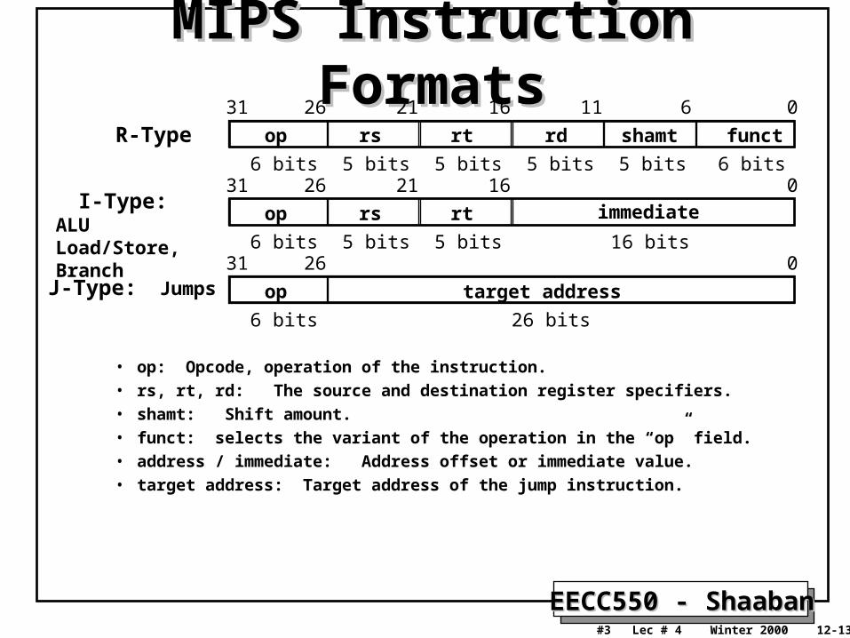
MIPS Instruction FormatsMIPS Instruction Formats
• op: Opcode, operation of the instruction.
• rs, rt, rd: The source and destination register specifiers.
• shamt: Shift amount.
• funct: selects the variant of the operation in the “op” field.
• address / immediate: Address offset or immediate value.
• target address: Target address of the jump instruction.
op target address
02631
6 bits 26 bits
op rs rt rd shamt funct
061116212631
6 bits 6 bits5 bits5 bits5 bits5 bits
op rs rt immediate
016212631
6 bits 16 bits5 bits5 bits
R-Type
I-Type: ALULoad/Store, Branch
J-Type: Jumps
EECC550 - ShaabanEECC550 - Shaaban#4 Lec # 4 Winter 2000 12-13-2000
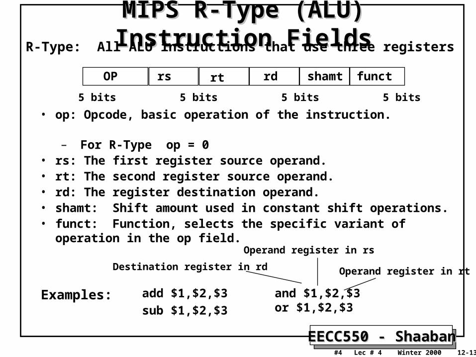
MIPS R-Type (ALU) Instruction FieldsMIPS R-Type (ALU) Instruction Fields
• op: Opcode, basic operation of the instruction. – For R-Type op = 0
• rs: The first register source operand.• rt: The second register source operand.• rd: The register destination operand.• shamt: Shift amount used in constant shift operations.• funct: Function, selects the specific variant of operation in the op
field.
OP rs rt rd shamt funct
6 bits 5 bits 5 bits 5 bits 5 bits 6 bits
R-Type: All ALU instructions that use three registers
add $1,$2,$3
sub $1,$2,$3
and $1,$2,$3or $1,$2,$3
Examples:
Destination register in rd Operand register in rt
Operand register in rs
EECC550 - ShaabanEECC550 - Shaaban#5 Lec # 4 Winter 2000 12-13-2000
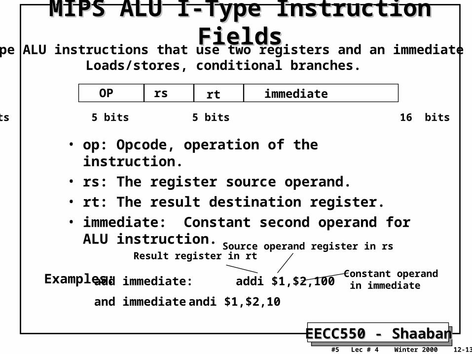
MIPS ALU I-Type Instruction FieldsMIPS ALU I-Type Instruction FieldsI-Type ALU instructions that use two registers and an immediate value Loads/stores, conditional branches.
• op: Opcode, operation of the instruction.
• rs: The register source operand.
• rt: The result destination register.
• immediate: Constant second operand for ALU instruction.
OP rs rt immediate
6 bits 5 bits 5 bits 16 bits
add immediate: addi $1,$2,100
and immediate andi $1,$2,10
Examples:
Result register in rtSource operand register in rs
Constant operand in immediate
EECC550 - ShaabanEECC550 - Shaaban#6 Lec # 4 Winter 2000 12-13-2000
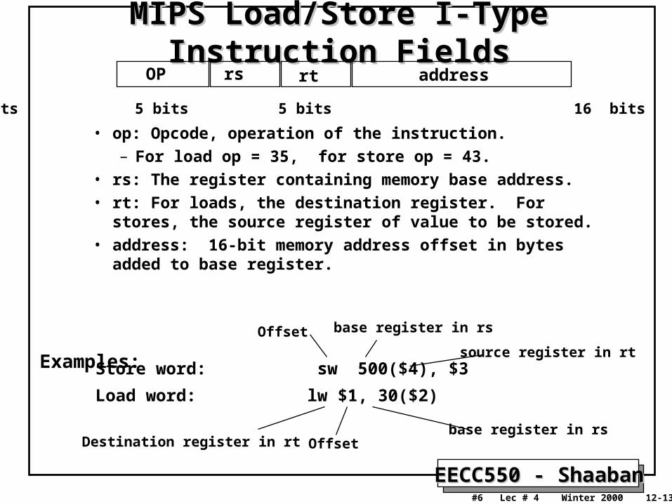
MIPS Load/Store I-Type Instruction FieldsMIPS Load/Store I-Type Instruction Fields
• op: Opcode, operation of the instruction.– For load op = 35, for store op = 43.
• rs: The register containing memory base address. • rt: For loads, the destination register. For stores, the source
register of value to be stored. • address: 16-bit memory address offset in bytes added to base
register.
OP rs rt address
6 bits 5 bits 5 bits 16 bits
Store word: sw 500($4), $3
Load word: lw $1, 30($2)
Examples:
Offset base register in rs
source register in rt
Destination register in rt Offsetbase register in rs
EECC550 - ShaabanEECC550 - Shaaban#7 Lec # 4 Winter 2000 12-13-2000
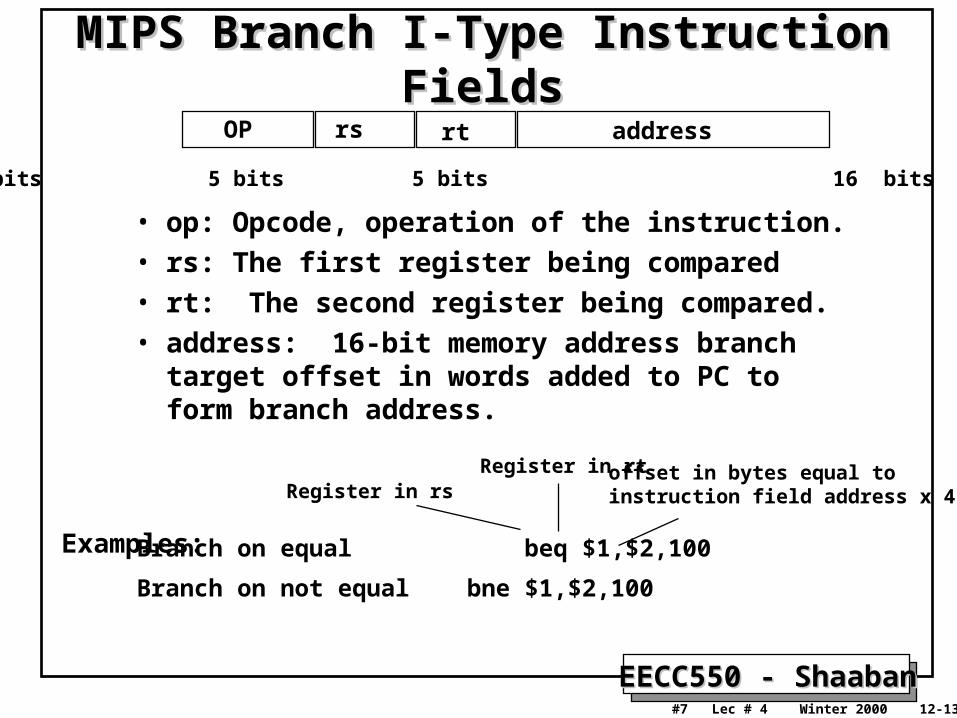
MIPS Branch I-Type Instruction FieldsMIPS Branch I-Type Instruction Fields
• op: Opcode, operation of the instruction.
• rs: The first register being compared
• rt: The second register being compared.
• address: 16-bit memory address branch target offset in words added to PC to form branch address.
OP rs rt address
6 bits 5 bits 5 bits 16 bits
Branch on equal beq $1,$2,100
Branch on not equal bne $1,$2,100
Examples:
Register in rsRegister in rt offset in bytes equal to
instruction field address x 4
EECC550 - ShaabanEECC550 - Shaaban#8 Lec # 4 Winter 2000 12-13-2000
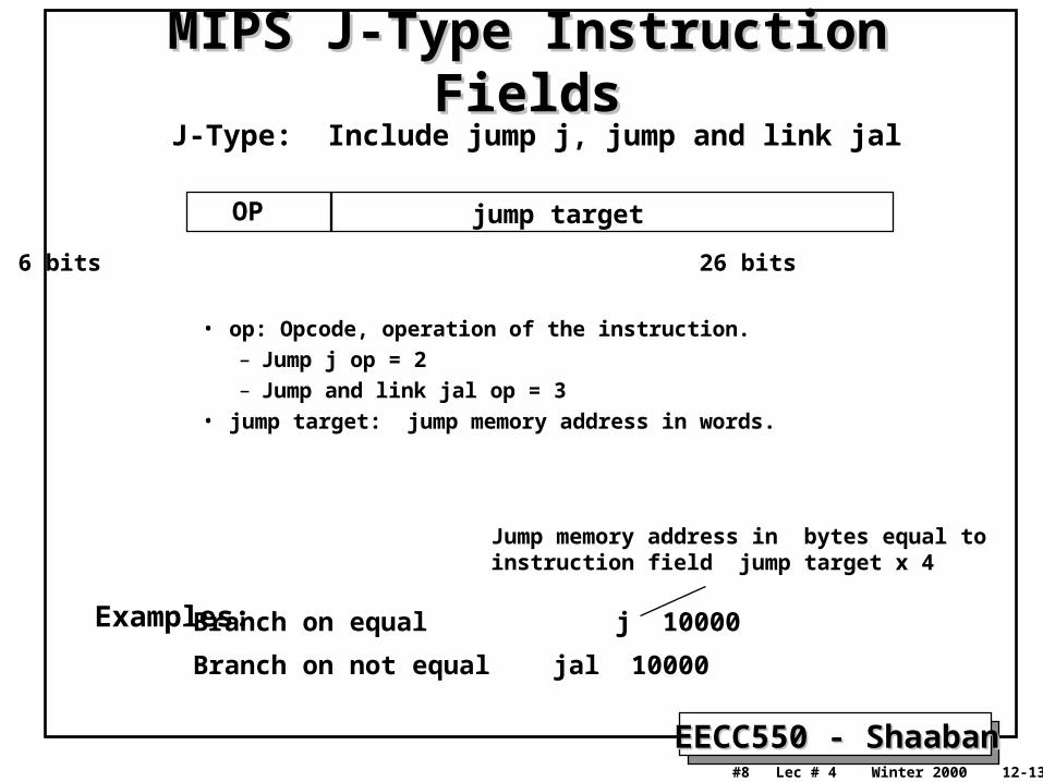
MIPS J-Type Instruction FieldsMIPS J-Type Instruction Fields
• op: Opcode, operation of the instruction.– Jump j op = 2– Jump and link jal op = 3
• jump target: jump memory address in words.
J-Type: Include jump j, jump and link jal
OP jump target
6 bits 26 bits
Branch on equal j 10000
Branch on not equal jal 10000
Examples:
Jump memory address in bytes equal toinstruction field jump target x 4
EECC550 - ShaabanEECC550 - Shaaban#9 Lec # 4 Winter 2000 12-13-2000
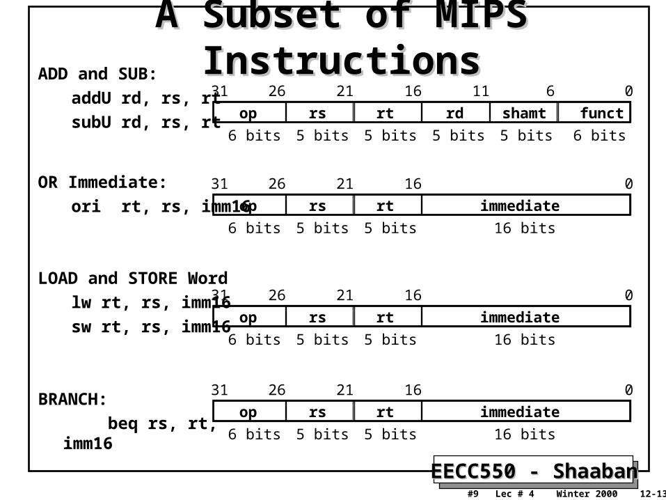
A Subset of MIPS InstructionsA Subset of MIPS InstructionsADD and SUB:
addU rd, rs, rt
subU rd, rs, rt
OR Immediate:
ori rt, rs, imm16
LOAD and STORE Word
lw rt, rs, imm16
sw rt, rs, imm16
BRANCH:
beq rs, rt, imm16
op rs rt rd shamt funct
061116212631
6 bits 6 bits5 bits5 bits5 bits5 bits
op rs rt immediate
016212631
6 bits 16 bits5 bits5 bits
op rs rt immediate
016212631
6 bits 16 bits5 bits5 bits
op rs rt immediate
016212631
6 bits 16 bits5 bits5 bits

EECC550 - ShaabanEECC550 - Shaaban#10 Lec # 4 Winter 2000 12-13-2000
Instruction Processing StepsInstruction Processing Steps
Obtain instruction from program storage
Determine instruction type
Obtain operands from registers
Compute result value or status
Store result in register/memory if needed
(usually called Write Back).
Update program counter to address
of next instruction}
Commonsteps for all instructions
Instruction
Fetch
Instruction
Decode
Execute
Result
Store
Next
Instruction
EECC550 - ShaabanEECC550 - Shaaban#11 Lec # 4 Winter 2000 12-13-2000
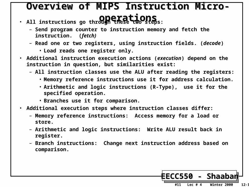
Overview of MIPS Instruction Micro-operationsOverview of MIPS Instruction Micro-operations• All instructions go through these two steps:
– Send program counter to instruction memory and fetch the instruction. (fetch)
– Read one or two registers, using instruction fields. (decode)• Load reads one register only.
• Additional instruction execution actions (execution) depend on the instruction in question, but similarities exist:– All instruction classes use the ALU after reading the registers:
• Memory reference instructions use it for address calculation.• Arithmetic and logic instructions (R-Type), use it for the specified
operation.• Branches use it for comparison.
• Additional execution steps where instruction classes differ:– Memory reference instructions: Access memory for a load or store.– Arithmetic and logic instructions: Write ALU result back in register.– Branch instructions: Change next instruction address based on
comparison.
EECC550 - ShaabanEECC550 - Shaaban#12 Lec # 4 Winter 2000 12-13-2000
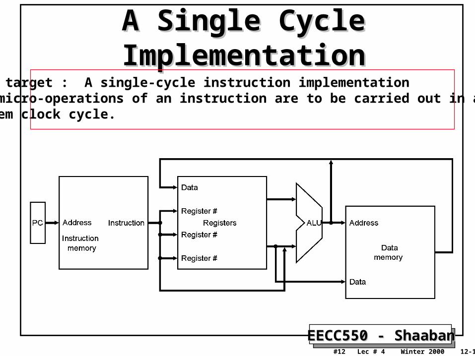
A Single Cycle ImplementationA Single Cycle ImplementationDesign target : A single-cycle instruction implementation All micro-operations of an instruction are to be carried out in a single system clock cycle.
EECC550 - ShaabanEECC550 - Shaaban#13 Lec # 4 Winter 2000 12-13-2000
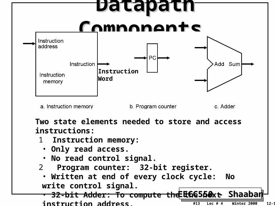
Datapath ComponentsDatapath Components
Two state elements needed to store and access instructions:1 Instruction memory: • Only read access.• No read control signal.
2 Program counter: 32-bit register.• Written at end of every clock cycle: No write control signal.• 32-bit Adder: To compute the the next instruction address.
InstructionWord
EECC550 - ShaabanEECC550 - Shaaban#14 Lec # 4 Winter 2000 12-13-2000
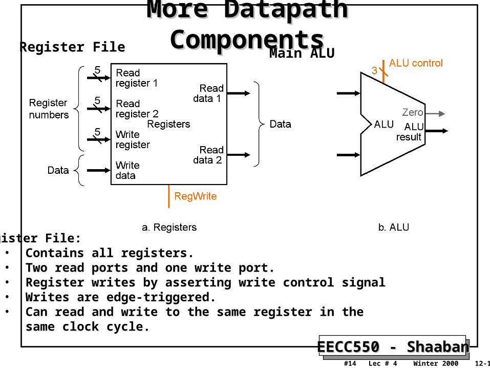
More Datapath ComponentsMore Datapath Components
Register File:• Contains all registers.• Two read ports and one write port.• Register writes by asserting write control signal• Writes are edge-triggered.• Can read and write to the same register in the same clock cycle.
Register File Main ALU
EECC550 - ShaabanEECC550 - Shaaban#15 Lec # 4 Winter 2000 12-13-2000
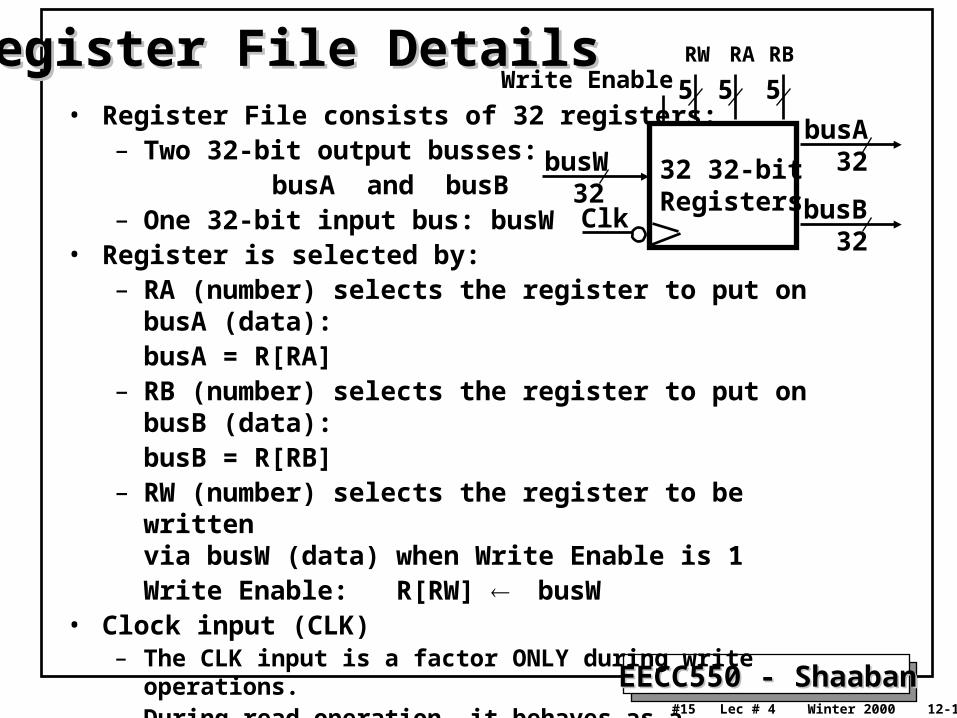
• Register File consists of 32 registers:– Two 32-bit output busses: busA and busB– One 32-bit input bus: busW
• Register is selected by:– RA (number) selects the register to put on busA (data):
busA = R[RA]– RB (number) selects the register to put on busB (data):
busB = R[RB]– RW (number) selects the register to be written
via busW (data) when Write Enable is 1Write Enable: R[RW] busW
• Clock input (CLK) – The CLK input is a factor ONLY during write operations.– During read operation, it behaves as a combinational logic block:
• RA or RB valid => busA or busB valid after “access time.”
Register File DetailsRegister File Details
Clk
busW
Write Enable
3232
busA
32busB
5 5 5
RW RA RB
32 32-bitRegisters
EECC550 - ShaabanEECC550 - Shaaban#16 Lec # 4 Winter 2000 12-13-2000
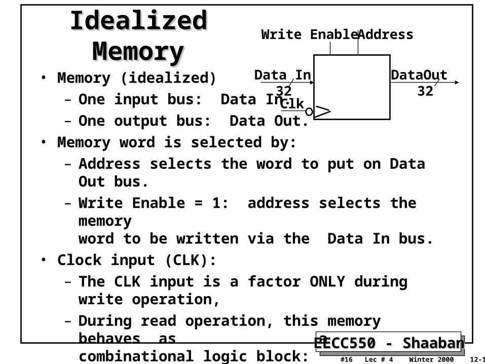
Idealized MemoryIdealized Memory
• Memory (idealized)
– One input bus: Data In.
– One output bus: Data Out.
• Memory word is selected by:
– Address selects the word to put on Data Out bus.
– Write Enable = 1: address selects the memoryword to be written via the Data In bus.
• Clock input (CLK):
– The CLK input is a factor ONLY during write operation,
– During read operation, this memory behaves as a combinational logic block:
• Address valid => Data Out valid after “access time.”
Clk
Data In
Write Enable
32 32DataOut
Address
EECC550 - ShaabanEECC550 - Shaaban#17 Lec # 4 Winter 2000 12-13-2000
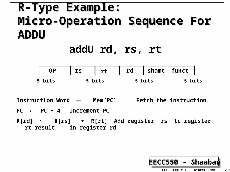
Instruction Word Mem[PC] Fetch the instruction
PC PC + 4 Increment PC
R[rd] R[rs] + R[rt] Add register rs to register rt result in register rd
R-Type Example:R-Type Example:Micro-Operation Sequence For ADDUMicro-Operation Sequence For ADDU
OP rs rt rd shamt funct
6 bits 5 bits 5 bits 5 bits 5 bits 6 bits
addU rd, rs, rt
EECC550 - ShaabanEECC550 - Shaaban#18 Lec # 4 Winter 2000 12-13-2000
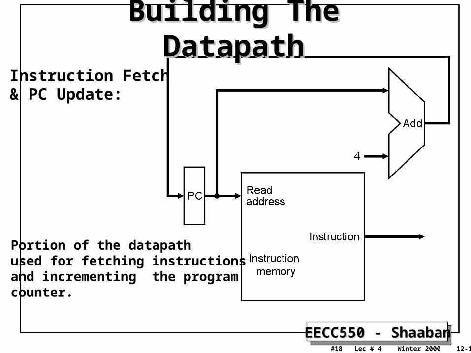
Building The DatapathBuilding The Datapath
Portion of the datapath used for fetching instructionsand incrementing the program counter.
Instruction Fetch& PC Update:
EECC550 - ShaabanEECC550 - Shaaban#19 Lec # 4 Winter 2000 12-13-2000
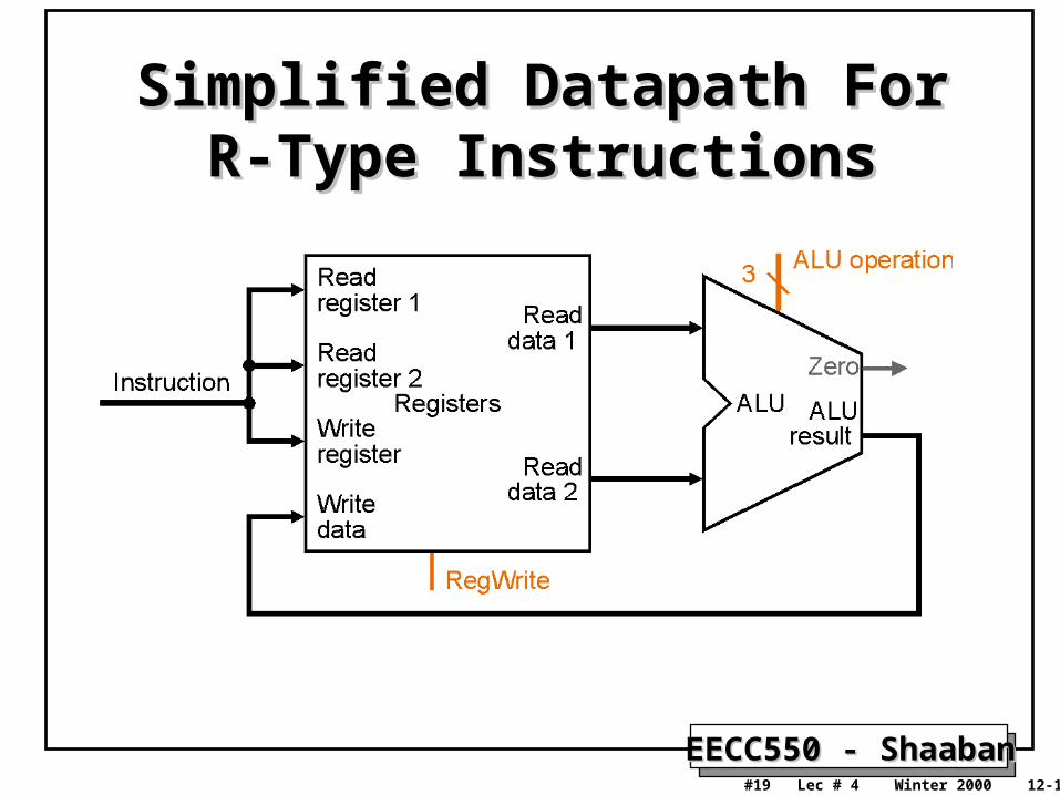
Simplified Datapath For R-Type Simplified Datapath For R-Type InstructionsInstructions
EECC550 - ShaabanEECC550 - Shaaban#20 Lec # 4 Winter 2000 12-13-2000
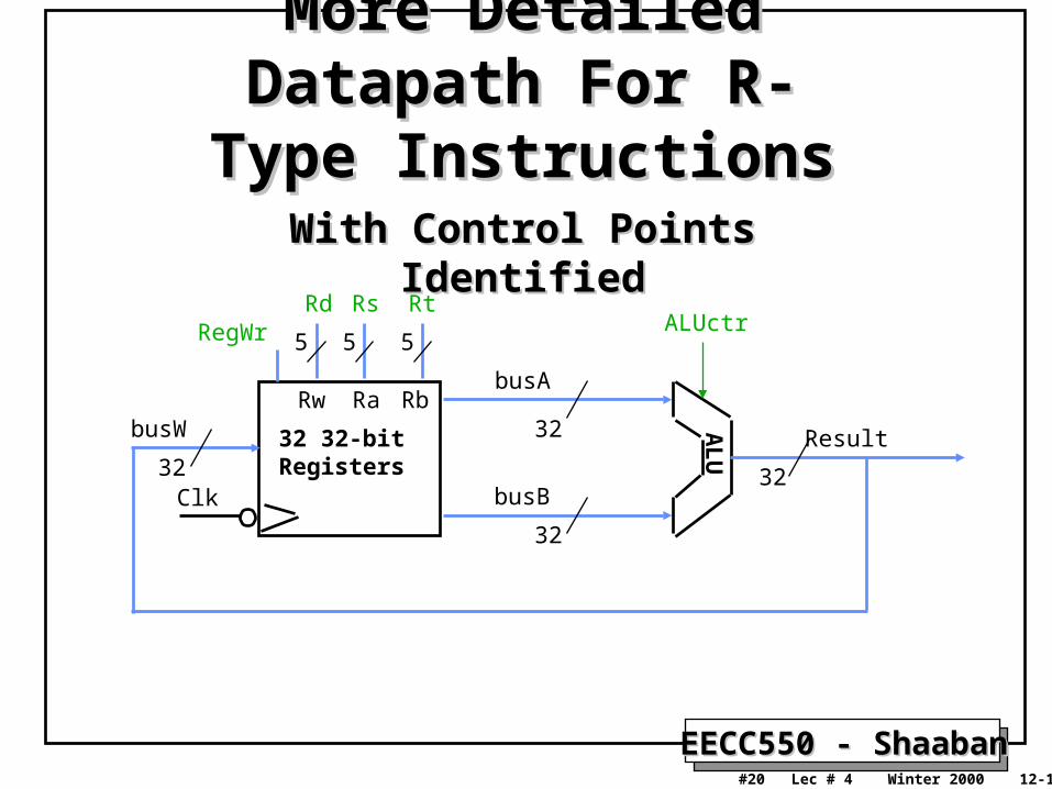
More Detailed Datapath More Detailed Datapath For R-Type InstructionsFor R-Type Instructions
With Control Points IdentifiedWith Control Points Identified
32
Result
ALUctr
Clk
busW
RegWr
32
32
busA
32
busB
5 5 5
Rw Ra Rb
32 32-bitRegisters
Rs RtRd
AL
U
EECC550 - ShaabanEECC550 - Shaaban#21 Lec # 4 Winter 2000 12-13-2000
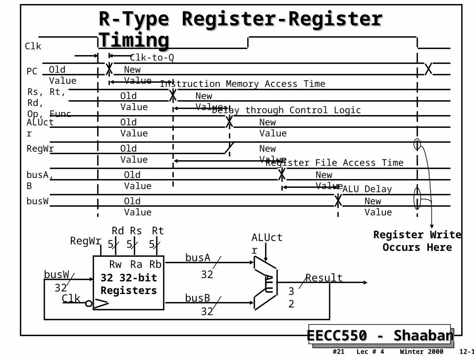
R-Type Register-Register TimingR-Type Register-Register Timing
32Result
ALUctr
Clk
busW
RegWr
3232
busA
32busB
5 5 5
Rw Ra Rb32 32-bitRegisters
Rs RtRd
AL
U
Clk
PC
Rs, Rt, Rd,Op, Func
Clk-to-Q
ALUctr
Instruction Memory Access Time
Old Value
New Value
RegWr Old Value
New Value
Delay through Control Logic
busA, B
Register File Access TimeOld Value
New Value
busWALU Delay
Old Value
New Value
Old Value
New Value
New ValueOld Value
Register WriteOccurs Here
EECC550 - ShaabanEECC550 - Shaaban#22 Lec # 4 Winter 2000 12-13-2000
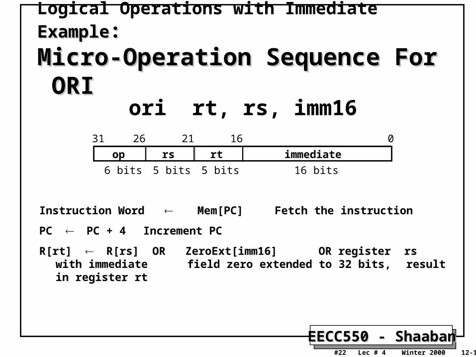
Instruction Word Mem[PC] Fetch the instruction
PC PC + 4 Increment PC
R[rt] R[rs] OR ZeroExt[imm16] OR register rs with immediate field zero extended to 32 bits, result in register rt
Logical Operations with Immediate Example Example::
Micro-Operation Sequence For ORIMicro-Operation Sequence For ORI
op rs rt immediate
016212631
6 bits 16 bits5 bits5 bits
ori rt, rs, imm16
EECC550 - ShaabanEECC550 - Shaaban#23 Lec # 4 Winter 2000 12-13-2000
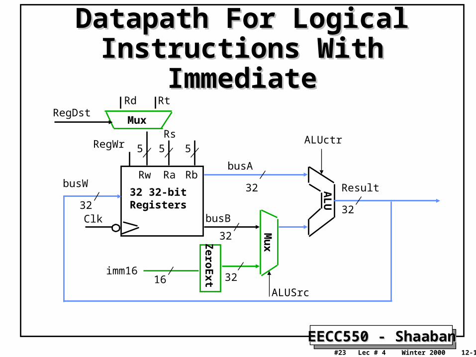
Datapath For Logical Datapath For Logical Instructions With ImmediateInstructions With Immediate
32
Result
ALUctr
Clk
busW
RegWr
32
32
busA
32
busB
5 5 5
Rw Ra Rb
32 32-bitRegisters
Rs
RtRdRegDst
ZeroE
xt
Mu
x
Mux
3216imm16
ALUSrc
AL
U
EECC550 - ShaabanEECC550 - Shaaban#24 Lec # 4 Winter 2000 12-13-2000
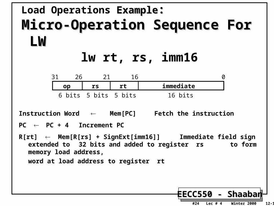
Instruction Word Mem[PC] Fetch the instruction
PC PC + 4 Increment PC
R[rt] Mem[R[rs] + SignExt[imm16]] Immediate field sign extended to 32 bits and added to register rs to form memory load address,
word at load address to register rt
Load Operations ExampleExample::
Micro-Operation Sequence For LWMicro-Operation Sequence For LW
op rs rt immediate
016212631
6 bits 16 bits5 bits5 bits
lw rt, rs, imm16
EECC550 - ShaabanEECC550 - Shaaban#25 Lec # 4 Winter 2000 12-13-2000
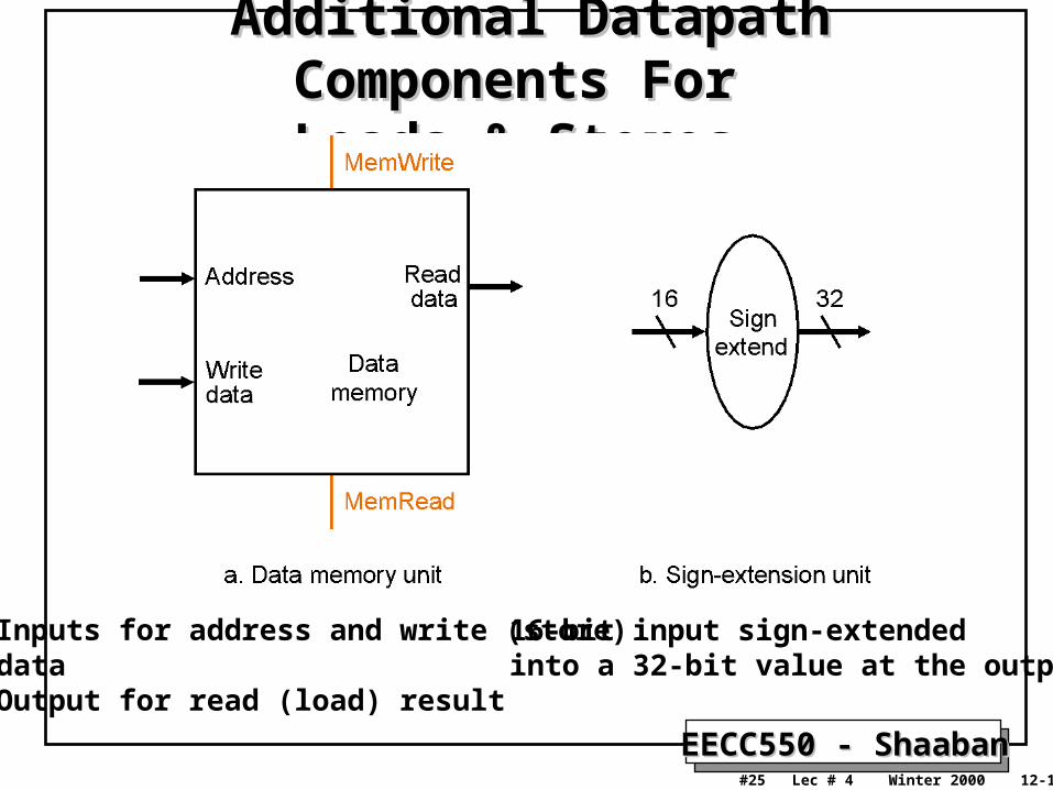
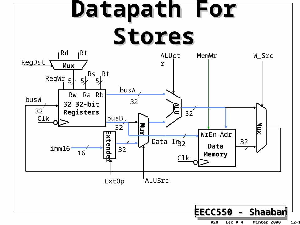
Additional Datapath Components For Additional Datapath Components For Loads & StoresLoads & Stores
Inputs for address and write (store)dataOutput for read (load) result
16-bit input sign-extended into a 32-bit value at the output
EECC550 - ShaabanEECC550 - Shaaban#26 Lec # 4 Winter 2000 12-13-2000
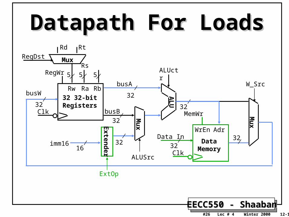
Datapath For LoadsDatapath For Loads
32
ALUctr
Clk
busW
RegWr
32
32
busA
32
busB
5 5 5
Rw Ra Rb
32 32-bitRegisters
Rs
RtRd
RegDst
Exten
der
Mu
x
Mux
3216
imm16
ALUSrc
ExtOp
Clk
Data InWrEn
32
Adr
DataMemory
32
AL
UMemWr M
ux
W_Src
EECC550 - ShaabanEECC550 - Shaaban#27 Lec # 4 Winter 2000 12-13-2000
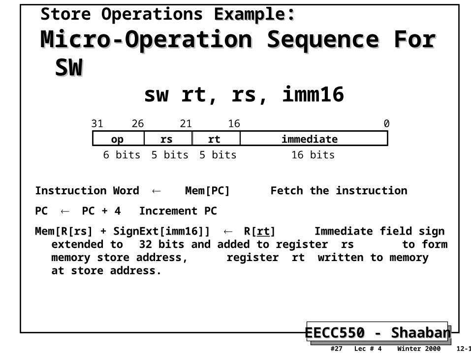
Instruction Word Mem[PC] Fetch the instruction
PC PC + 4 Increment PC
Mem[R[rs] + SignExt[imm16]] R[rt] Immediate field sign extended to 32 bits and added to register rs
to form memory store address,register rt written to memory at store address.
Store Operations ExampleExample::
Micro-Operation Sequence For SWMicro-Operation Sequence For SW
op rs rt immediate
016212631
6 bits 16 bits5 bits5 bits
sw rt, rs, imm16
EECC550 - ShaabanEECC550 - Shaaban#28 Lec # 4 Winter 2000 12-13-2000
Datapath For StoresDatapath For Stores
ALUSrcExtOp
32
ALUctr
Clk
busW
RegWr
32
32
busA
32
busB
55 5
Rw Ra Rb
32 32-bitRegisters
Rs
Rt
Rt
Rd
RegDst
Exten
der
Mu
x
Mux
3216imm16
Clk
Data InWrEn
32
Adr
DataMemory
MemWr
AL
U
32
Mu
x
W_Src
EECC550 - ShaabanEECC550 - Shaaban#29 Lec # 4 Winter 2000 12-13-2000
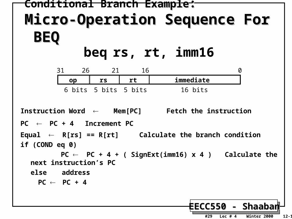
Instruction Word Mem[PC] Fetch the instruction
PC PC + 4 Increment PC
Equal R[rs] == R[rt] Calculate the branch condition
if (COND eq 0)
PC PC + 4 + ( SignExt(imm16) x 4 ) Calculate the next instruction’s PC
else address
PC PC + 4
Conditional Branch ExampleExample::
Micro-Operation Sequence For BEQMicro-Operation Sequence For BEQ
op rs rt immediate
016212631
6 bits 16 bits5 bits5 bits
beq rs, rt, imm16
EECC550 - ShaabanEECC550 - Shaaban#30 Lec # 4 Winter 2000 12-13-2000
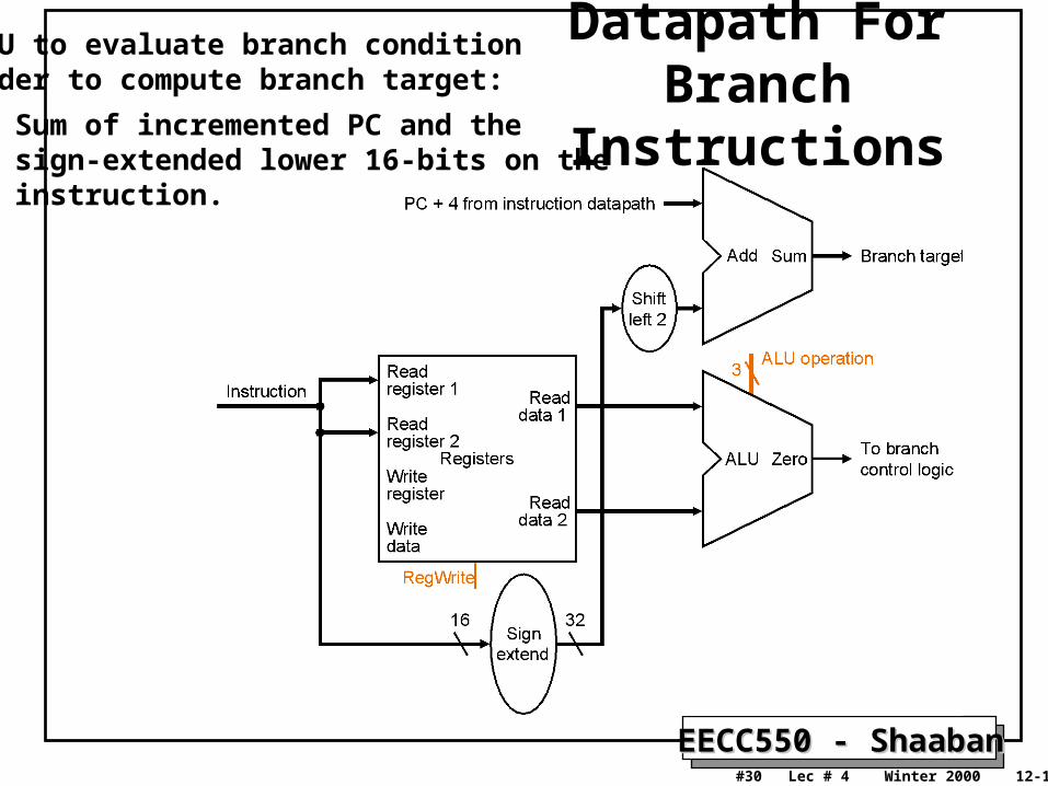
Datapath For Branch Instructions
ALU to evaluate branch conditionAdder to compute branch target:
• Sum of incremented PC and the sign-extended lower 16-bits on the instruction.
EECC550 - ShaabanEECC550 - Shaaban#31 Lec # 4 Winter 2000 12-13-2000
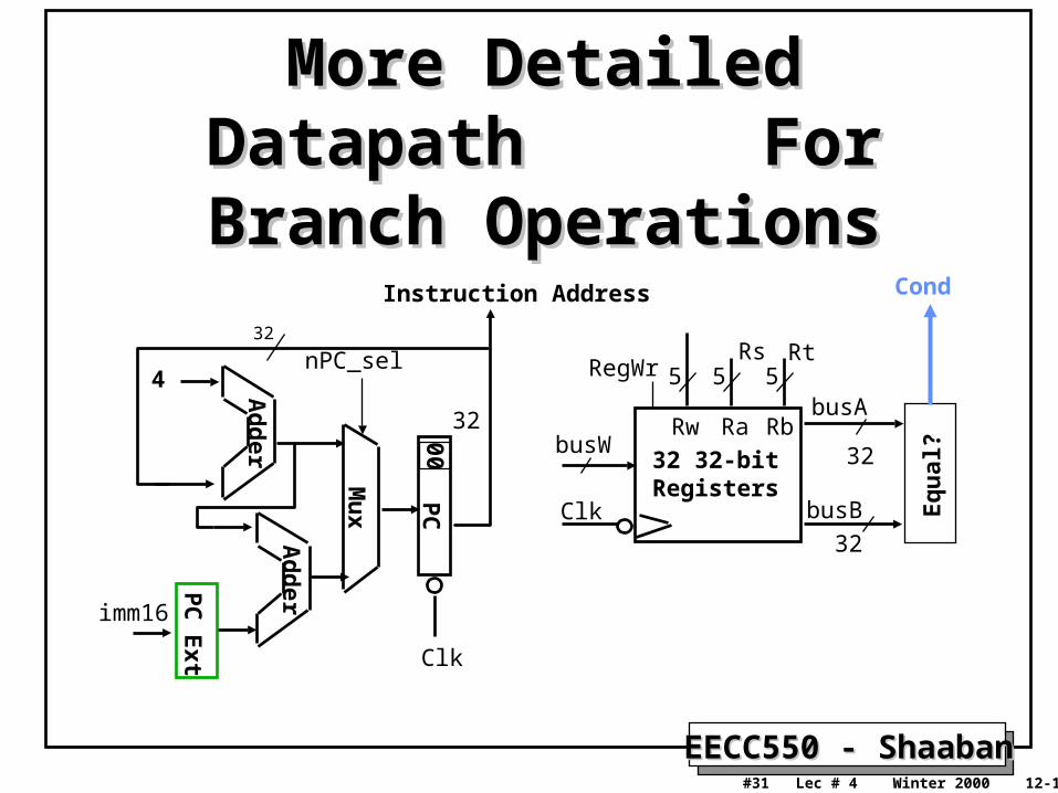
More Detailed Datapath More Detailed Datapath For Branch Operations For Branch Operations
Clk
busW
RegWr
32
busA
32
busB
5 5 5
Rw Ra Rb
32 32-bitRegisters
Rs Rt
Eq
ual
?
Cond
32
imm16P
CClk
00
Ad
der
Mu
x
Ad
der
4nPC_sel
PC
Ext
Instruction Address
32
EECC550 - ShaabanEECC550 - Shaaban#32 Lec # 4 Winter 2000 12-13-2000
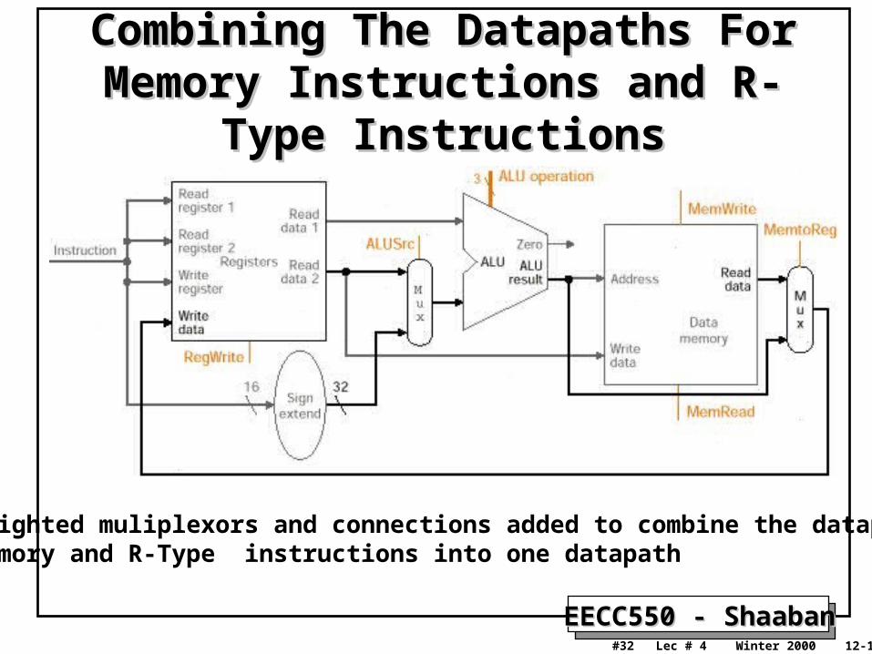
Combining The Datapaths For Memory Combining The Datapaths For Memory Instructions and R-Type InstructionsInstructions and R-Type Instructions
Highlighted muliplexors and connections added to combine the datapaths of memory and R-Type instructions into one datapath
EECC550 - ShaabanEECC550 - Shaaban#33 Lec # 4 Winter 2000 12-13-2000
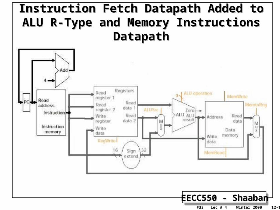
Instruction Fetch Datapath Added toInstruction Fetch Datapath Added toALU R-Type and Memory Instructions DatapathALU R-Type and Memory Instructions Datapath
EECC550 - ShaabanEECC550 - Shaaban#34 Lec # 4 Winter 2000 12-13-2000
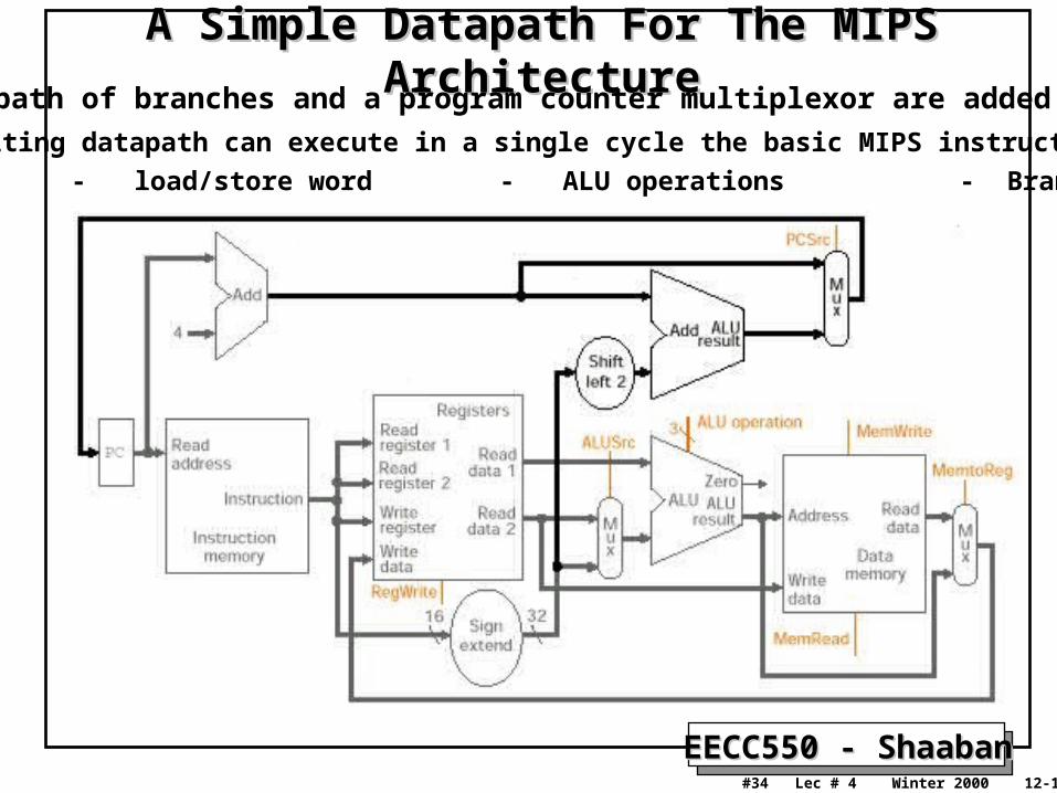
A Simple Datapath For The MIPS ArchitectureA Simple Datapath For The MIPS ArchitectureDatapath of branches and a program counter multiplexor are added.
Resulting datapath can execute in a single cycle the basic MIPS instruction:
- load/store word - ALU operations - Branches
EECC550 - ShaabanEECC550 - Shaaban#35 Lec # 4 Winter 2000 12-13-2000
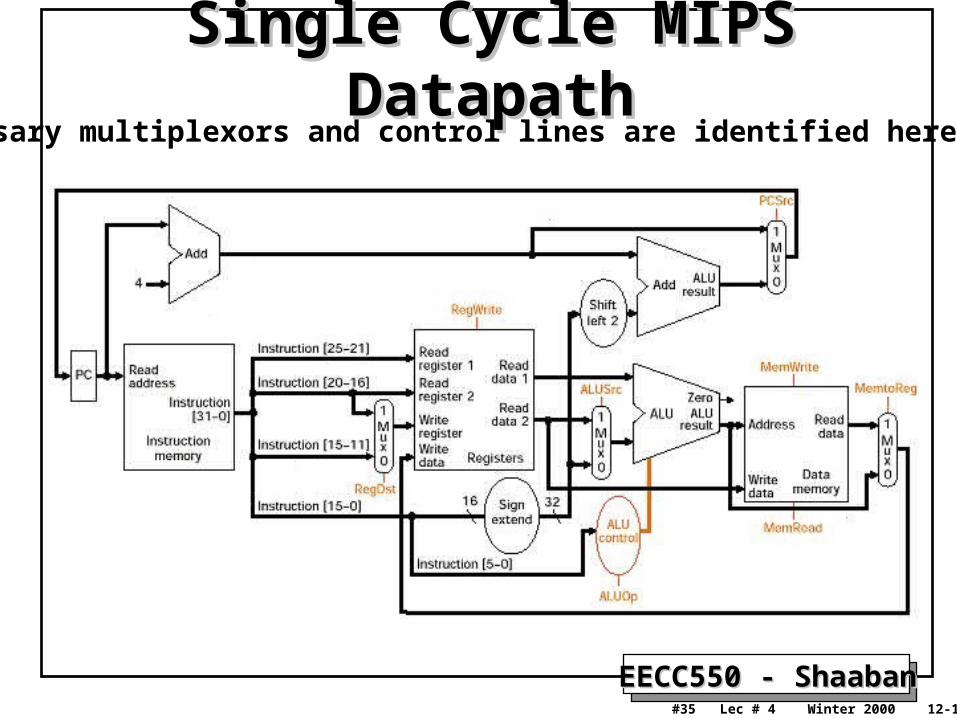
Single Cycle MIPS DatapathSingle Cycle MIPS DatapathNecessary multiplexors and control lines are identified here:
EECC550 - ShaabanEECC550 - Shaaban#36 Lec # 4 Winter 2000 12-13-2000
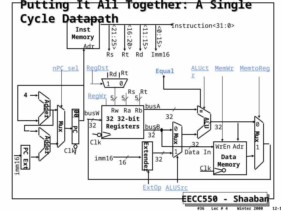
Putting It All Together: A Single Cycle DatapathPutting It All Together: A Single Cycle Datapathim
m16
32
ALUctr
Clk
busW
RegWr
32
32
busA
32busB
55 5
Rw Ra Rb32 32-bitRegisters
Rs
Rt
Rt
RdRegDst
Exten
der
Mu
x
3216imm16
ALUSrcExtOp
Mu
x
MemtoReg
Clk
Data InWrEn32 Adr
DataMemory
MemWrA
LU
Equal
Instruction<31:0>
0
1
0
1
01
<21:25>
<16:20>
<11:15>
<0:15>
Imm16RdRtRs
=
Ad
der
Ad
der
PC
Clk
00
Mu
x
4
nPC_sel
PC
Ext
Adr
InstMemory
EECC550 - ShaabanEECC550 - Shaaban#37 Lec # 4 Winter 2000 12-13-2000
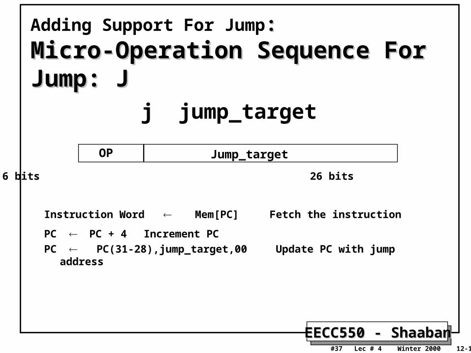
Instruction Word Mem[PC] Fetch the instruction
PC PC + 4 Increment PC
PC PC(31-28),jump_target,00 Update PC with jump address
Adding Support For Jump::
Micro-Operation Sequence For Jump: JMicro-Operation Sequence For Jump: J
OP Jump_target
6 bits 26 bits
j jump_target
EECC550 - ShaabanEECC550 - Shaaban#38 Lec # 4 Winter 2000 12-13-2000
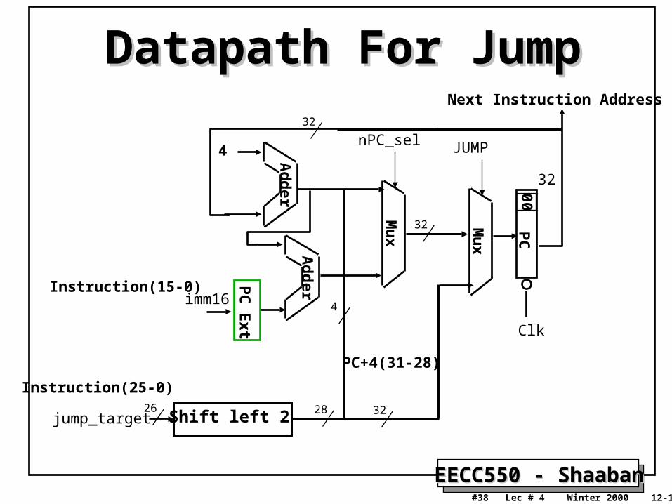
Datapath For JumpDatapath For Jump
32
PC
Clk
00
Mu
x
nPC_sel
imm16
Ad
der
Ad
der
4
PC
Ext
Next Instruction Address
Mu
x
JUMP
Shift left 2jump_target
Instruction(15-0)
Instruction(25-0)
32
26
PC+4(31-28)
28 32
4
32
EECC550 - ShaabanEECC550 - Shaaban#39 Lec # 4 Winter 2000 12-13-2000
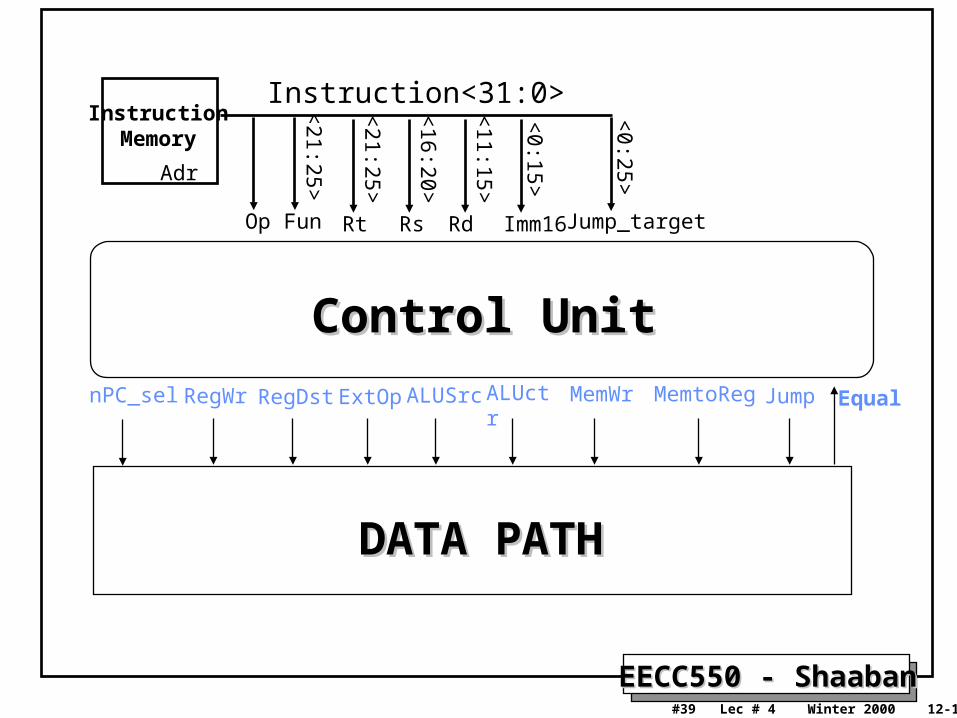
RegDst ALUctrALUSrc MemtoReg Equal
Instruction<31:0>
<21:25>
<16:20>
<11:15>
<0:15>
Imm16RdRsRt
Adr
InstructionMemory
DATA PATHDATA PATH
ExtOp MemWr
Control UnitControl Unit
Op
<21:25>
Fun
nPC_sel RegWr
<0:25>
Jump_target
Jump
EECC550 - ShaabanEECC550 - Shaaban#40 Lec # 4 Winter 2000 12-13-2000
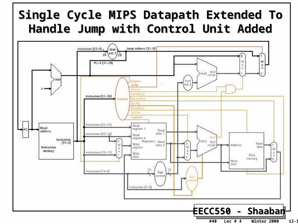
Single Cycle MIPS Datapath Extended To Handle Single Cycle MIPS Datapath Extended To Handle Jump with Control Unit AddedJump with Control Unit Added
EECC550 - ShaabanEECC550 - Shaaban#41 Lec # 4 Winter 2000 12-13-2000
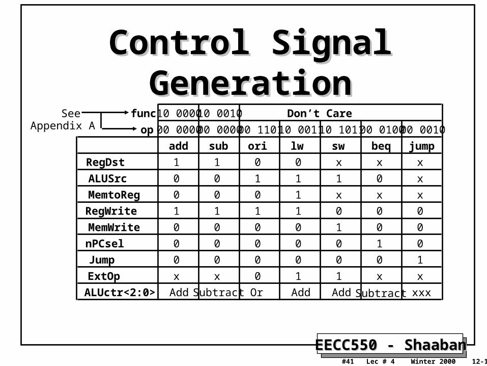
Control Signal GenerationControl Signal Generation
add sub ori lw sw beq jump
RegDst
ALUSrc
MemtoReg
RegWrite
MemWrite
nPCsel
Jump
ExtOp
ALUctr<2:0>
1
0
0
1
0
0
0
x
Add
1
0
0
1
0
0
0
x
Subtract
0
1
0
1
0
0
0
0
Or
0
1
1
1
0
0
0
1
Add
x
1
x
0
1
0
0
1
Add
x
0
x
0
0
1
0
x
Subtract
x
x
x
0
0
0
1
x
xxx
func
op 00 0000 00 0000 00 1101 10 0011 10 1011 00 0100 00 0010Appendix A10 0000See 10 0010 Don’t Care
EECC550 - ShaabanEECC550 - Shaaban#42 Lec # 4 Winter 2000 12-13-2000
The Concept of Local DecodingThe Concept of Local Decoding
R-type ori lw sw beq jump
RegDst
ALUSrc
MemtoReg
RegWrite
MemWrite
Branch
Jump
ExtOp
ALUop<N:0>
1
0
0
1
0
0
0
x
“R-type”
0
1
0
1
0
0
0
0
Or
0
1
1
1
0
0
0
1
Add
x
1
x
0
1
0
0
1
Add
x
0
x
0
0
1
0
x
Subtract
x
x
x
0
0
0
1
x
xxx
op 00 0000 00 1101 10 0011 10 1011 00 0100 00 0010
MainControl
op
6
ALUControl(Local)
func
N
6ALUop
ALUctr
3
AL
U
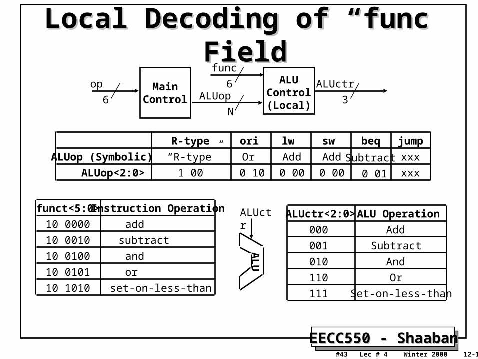
EECC550 - ShaabanEECC550 - Shaaban#43 Lec # 4 Winter 2000 12-13-2000
Local Decoding of “func” FieldLocal Decoding of “func” Field
R-type ori lw sw beq jump
ALUop (Symbolic) “R-type” Or Add Add Subtract xxx
ALUop<2:0> 1 00 0 10 0 00 0 00 0 01 xxx
MainControl
op
6
ALUControl(Local)
func
N
6ALUop
ALUctr
3
funct<5:0> Instruction Operation
10 0000
10 0010
10 0100
10 0101
10 1010
add
subtract
and
or
set-on-less-than
ALUctr<2:0> ALU Operation
000
001
010
110
111
Add
Subtract
And
Or
Set-on-less-than
ALUctrA
LU
EECC550 - ShaabanEECC550 - Shaaban#44 Lec # 4 Winter 2000 12-13-2000
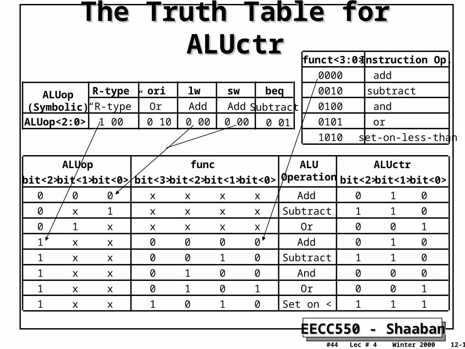
The Truth Table for ALUctrThe Truth Table for ALUctr
R-type ori lw sw beqALUop(Symbolic) “R-type” Or Add Add Subtract
ALUop<2:0> 1 00 0 10 0 00 0 00 0 01
ALUop func
bit<2> bit<1> bit<0> bit<2> bit<1> bit<0>bit<3>
0 0 0 x x x x
ALUctrALUOperation
Add 0 1 0
bit<2> bit<1> bit<0>
0 x 1 x x x x Subtract 1 1 0
0 1 x x x x x Or 0 0 1
1 x x 0 0 0 0 Add 0 1 0
1 x x 0 0 1 0 Subtract 1 1 0
1 x x 0 1 0 0 And 0 0 0
1 x x 0 1 0 1 Or 0 0 1
1 x x 1 0 1 0 Set on < 1 1 1
funct<3:0> Instruction Op.
0000
0010
0100
0101
1010
add
subtract
and
or
set-on-less-than
EECC550 - ShaabanEECC550 - Shaaban#45 Lec # 4 Winter 2000 12-13-2000
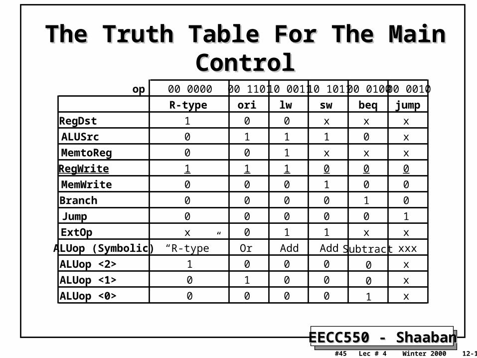
The Truth Table For The Main ControlThe Truth Table For The Main Control
R-type ori lw sw beq jump
RegDst
ALUSrc
MemtoReg
RegWrite
MemWrite
Branch
Jump
ExtOp
ALUop (Symbolic)
1
0
0
1
0
0
0
x
“R-type”
0
1
0
1
0
0
0
0
Or
0
1
1
1
0
0
0
1
Add
x
1
x
0
1
0
0
1
Add
x
0
x
0
0
1
0
x
Subtract
x
x
x
0
0
0
1
x
xxx
op 00 0000 00 1101 10 0011 10 1011 00 0100 00 0010
ALUop <2> 1 0 0 0 0 x
ALUop <1> 0 1 0 0 0 x
ALUop <0> 0 0 0 0 1 x
EECC550 - ShaabanEECC550 - Shaaban#46 Lec # 4 Winter 2000 12-13-2000
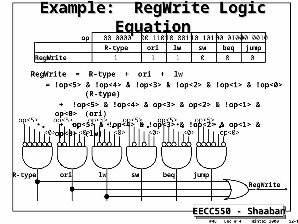
Example: RegWrite Logic EquationExample: RegWrite Logic Equation
R-type ori lw sw beq jump
RegWrite 1 1 1 0 0 0
op 00 0000 00 1101 10 0011 10 1011 00 0100 00 0010
RegWrite = R-type + ori + lw
= !op<5> & !op<4> & !op<3> & !op<2> & !op<1> & !op<0> (R-type)
+ !op<5> & !op<4> & op<3> & op<2> & !op<1> & op<0> (ori)
+ op<5> & !op<4> & !op<3> & !op<2> & op<1> & op<0> (lw)
op<0>
op<5>. .op<5>. .<0>
op<5>. .<0>
op<5>. .<0>
op<5>. .<0>
op<5>. .<0>
R-type ori lw sw beq jump
RegWrite
EECC550 - ShaabanEECC550 - Shaaban#47 Lec # 4 Winter 2000 12-13-2000
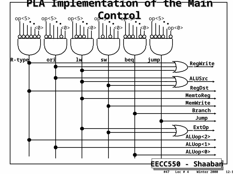
PLA Implementation of the Main ControlPLA Implementation of the Main Control
op<0>
op<5>. .op<5>. .<0>
op<5>. .<0>
op<5>. .<0>
op<5>. .<0>
op<5>. .<0>
R-type ori lw sw beq jumpRegWrite
ALUSrc
MemtoReg
MemWrite
Branch
Jump
RegDst
ExtOp
ALUop<2>
ALUop<1>
ALUop<0>
EECC550 - ShaabanEECC550 - Shaaban#48 Lec # 4 Winter 2000 12-13-2000
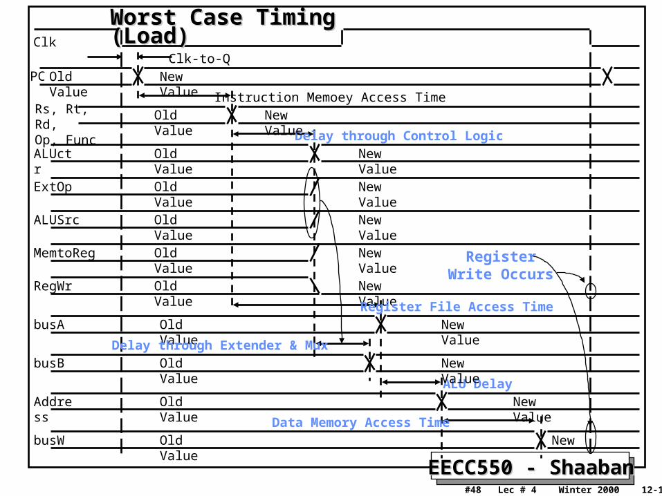
Clk
PC
Rs, Rt, Rd,Op, Func
Clk-to-Q
ALUctr
Instruction Memoey Access Time
Old Value New Value
RegWr Old Value New Value
Delay through Control Logic
busA
Register File Access Time
Old Value New Value
busB
ALU Delay
Old Value New Value
Old Value New Value
New ValueOld Value
ExtOp Old Value New Value
ALUSrc Old Value New Value
MemtoReg Old Value New Value
Address Old Value New Value
busW Old Value New
Delay through Extender & Mux
RegisterWrite Occurs
Data Memory Access Time
Worst Case Timing (Load)Worst Case Timing (Load)
EECC550 - ShaabanEECC550 - Shaaban#49 Lec # 4 Winter 2000 12-13-2000
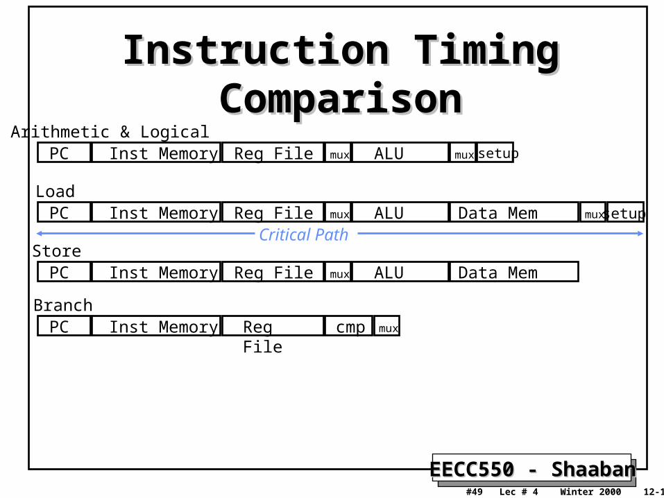
Instruction Timing ComparisonInstruction Timing Comparison
PC Inst Memory mux ALU Data Mem mux
PC Reg FileInst Memory mux ALU mux
PC Inst Memory mux ALU Data Mem
PC Inst Memory cmp mux
Reg File
Reg File
Reg File
Arithmetic & Logical
Load
Store
Branch
Critical Path
setup
setup
EECC550 - ShaabanEECC550 - Shaaban#50 Lec # 4 Winter 2000 12-13-2000
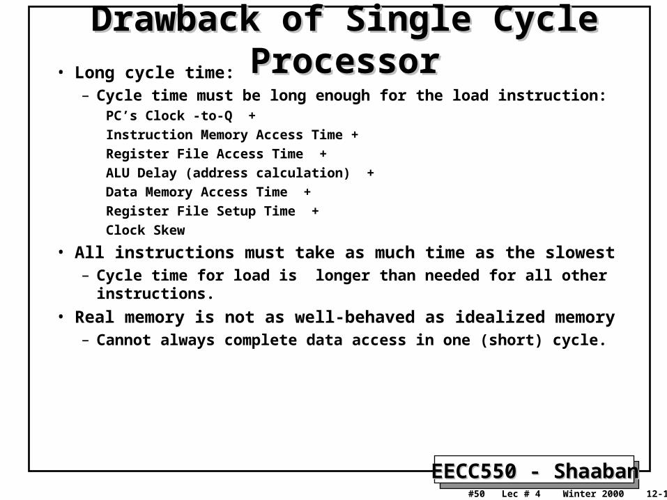
Drawback of Single Cycle ProcessorDrawback of Single Cycle Processor• Long cycle time:
– Cycle time must be long enough for the load instruction:PC’s Clock -to-Q +
Instruction Memory Access Time +
Register File Access Time +
ALU Delay (address calculation) +
Data Memory Access Time +
Register File Setup Time +
Clock Skew
• All instructions must take as much time as the slowest– Cycle time for load is longer than needed for all other
instructions.
• Real memory is not as well-behaved as idealized memory– Cannot always complete data access in one (short) cycle.