Embed Size (px)
Citation preview

EECC550 - ShaabanEECC550 - Shaaban#1 Lec # 9 Winter 2002 1-18-2003
Main MemoryMain Memory• Main memory generally utilizes Dynamic RAM (DRAM),
which use a single transistor to store a bit, but require a periodic data refresh by reading every row.
• Static RAM may be used for main memory if the added expense, low density, high power consumption, and complexity is feasible (e.g. Cray Vector Supercomputers).
• Main memory performance is affected by:
– Memory latency: Affects cache miss penalty. Measured by:• Access time: The time it takes between a memory access request is issued to
main memory and the time the requested information is available to cache/CPU.
• Cycle time: The minimum time between requests to memory
(greater than access time in DRAM to allow address lines to be stable)
– Memory bandwidth: The maximum sustained data transfer rate between main memory and cache/CPU.
EECC550 - ShaabanEECC550 - Shaaban#2 Lec # 9 Winter 2002 1-18-2003
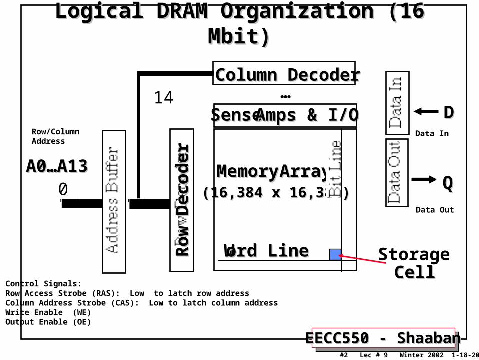
Logical DRAM Organization (16 Mbit)Logical DRAM Organization (16 Mbit)
Data In
Data Out
Column DecoderColumn Decoder
Sense Sense Amps & I/OAmps & I/O
Memory Memory ArrayArray(16,384 x 16,384)(16,384 x 16,384)
A0…A13A0…A130
…14DD
WWord Lineord Line Storage CellCell
Row
Dec
oder
Row
Dec
oder
Row/ColumnAddress
Control Signals:Row Access Strobe (RAS): Low to latch row addressColumn Address Strobe (CAS): Low to latch column addressWrite Enable (WE)Output Enable (OE)

EECC550 - ShaabanEECC550 - Shaaban#3 Lec # 9 Winter 2002 1-18-2003
Logical Diagram of A Typical DRAMLogical Diagram of A Typical DRAM

EECC550 - ShaabanEECC550 - Shaaban#4 Lec # 9 Winter 2002 1-18-2003
Four Key DRAM Timing ParametersFour Key DRAM Timing Parameters• tRAC: Minimum time from RAS (Row Access Strobe) line falling to the valid data output.
– Usually quoted as the nominal speed of a DRAM chip
– For a typical 64Mb DRAM tRAC = 60 ns
• tRC: Minimum time from the start of one row access to the start of the next (memory cycle time).
– tRC = 110 ns for a 64Mbit DRAM with a tRAC of 60 ns
• tCAC: minimum time from CAS (Column Access Strobe) line falling to valid data output.
– 12 ns for a 64Mbit DRAM with a tRAC of 60 ns
• tPC: minimum time from the start of one column access to the start of the next.
– About 25 ns for a 64Mbit DRAM with a tRAC of 60 ns

EECC550 - ShaabanEECC550 - Shaaban#5 Lec # 9 Winter 2002 1-18-2003
DRAM PerformanceDRAM Performance• A 60 ns (tRAC) DRAM chip can:
– Perform a row access only every 110 ns (tRC)
– Perform column access (tCAC) in 12 ns, but time between column accesses is at least 25 ns (tPC).
• In practice, external address delays and turning around buses make it 30 to 40 ns
• These times do not include the time to drive the addresses off the CPU or the memory controller overhead.
EECC550 - ShaabanEECC550 - Shaaban#6 Lec # 9 Winter 2002 1-18-2003
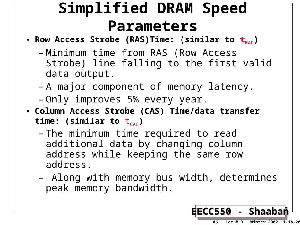
Simplified DRAM Speed Parameters
• Row Access Strobe (RAS)Time: (similar to tRAC)
– Minimum time from RAS (Row Access Strobe) line falling to the first valid data output.
– A major component of memory latency.– Only improves 5% every year.
• Column Access Strobe (CAS) Time/data transfer time: (similar to tCAC)
– The minimum time required to read additional data by changing column address while keeping the same row address.
– Along with memory bus width, determines peak memory bandwidth.

EECC550 - ShaabanEECC550 - Shaaban#7 Lec # 9 Winter 2002 1-18-2003
DRAM Generations
Year Size RAS (ns) CAS (ns) Cycle Time Memory Type
1980 64 Kb 150-180 75 250 ns Page Mode1983 256 Kb 120-150 50 220 ns Page Mode1986 1 Mb 100-120 25 190 ns1989 4 Mb 80-100 20 165 ns Fast Page Mode1992 16 Mb 60-80 15 120 ns EDO 1996 64 Mb 50-70 12 110 ns PC66 SDRAM1998 128 Mb 50-70 10 100 ns PC100 SDRAM2000 256 Mb 45-65 7 90 ns PC133 SDRAM2002 512 Mb 40-60 5 80 ns PC2700 DDR SDRAM
8000:1 15:1 3:1 (Capacity) (~bandwidth) (Latency)

EECC550 - ShaabanEECC550 - Shaaban#8 Lec # 9 Winter 2002 1-18-2003
Page Mode DRAMPage Mode DRAM

EECC550 - ShaabanEECC550 - Shaaban#9 Lec # 9 Winter 2002 1-18-2003
Page Mode DRAM Write TimingPage Mode DRAM Write Timing
EECC550 - ShaabanEECC550 - Shaaban#10 Lec # 9 Winter 2002 1-18-2003
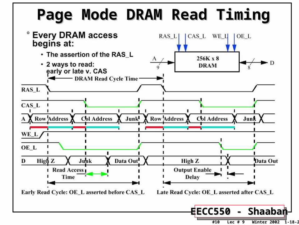
Page Mode DRAM Read TimingPage Mode DRAM Read Timing

EECC550 - ShaabanEECC550 - Shaaban#11 Lec # 9 Winter 2002 1-18-2003
Simplified Asynchronous Page Mode DRAM Simplified Asynchronous Page Mode DRAM Read TimingRead Timing
Source: http://arstechnica.com/paedia/r/ram_guide/ram_guide.part2-1.html

EECC550 - ShaabanEECC550 - Shaaban#12 Lec # 9 Winter 2002 1-18-2003
Fast Page Mode DRAMFast Page Mode DRAM

EECC550 - ShaabanEECC550 - Shaaban#13 Lec # 9 Winter 2002 1-18-2003
Simplified Asynchronous Fast Page Mode Simplified Asynchronous Fast Page Mode (FPM) DRAM Read Timing(FPM) DRAM Read Timing
Typical timing at 66 MHZ : 5-3-3-3For bus width = 64 bits = 8 bytes cache block size = 32 bytesIt takes = 5+3+3+3 = 14 memory cycles or 15 ns x 14 = 210 ns to read 32 byte blockRead Miss penalty for CPU running at 1 GHZ = 15 x 14 = 210 CPU cycles
FPM DRAM speed rated using tRAC ~ 50-70ns

EECC550 - ShaabanEECC550 - Shaaban#14 Lec # 9 Winter 2002 1-18-2003
• Extended Data Out DRAM operates in a similar fashion to Fast Page Mode DRAM except the data from one read is on the output pins at the same time the column address for the next read is being latched in.
Simplified Asynchronous Extended Data Out (EDO) Simplified Asynchronous Extended Data Out (EDO) DRAM Read TimingDRAM Read Timing
Source: http://arstechnica.com/paedia/r/ram_guide/ram_guide.part2-1.html
Typical timing at 66 MHZ : 5-2-2-2For bus width = 64 bits = 8 bytes Max. Bandwidth = 8 x 66 / 2 = 264 Mbytes/sec It takes = 5+2+2+2 = 11 memory cycles or 15 ns x 11 = 165 ns to read 32 byte cache blockMinimum Read Miss penalty for CPU running at 1 GHZ = 11 x 15 = 165 CPU cycles
EDO DRAM speed rated using tRAC ~ 40-60ns

EECC550 - ShaabanEECC550 - Shaaban#15 Lec # 9 Winter 2002 1-18-2003
Memory Bandwidth Improvement TechniquesMemory Bandwidth Improvement Techniques• Wider Main Memory: Memory width is increased to a number of words (usually the size of a
cache block). Memory bandwidth is proportional to memory width.
e.g Doubling the width of cache and memory doubles
memory bandwidth
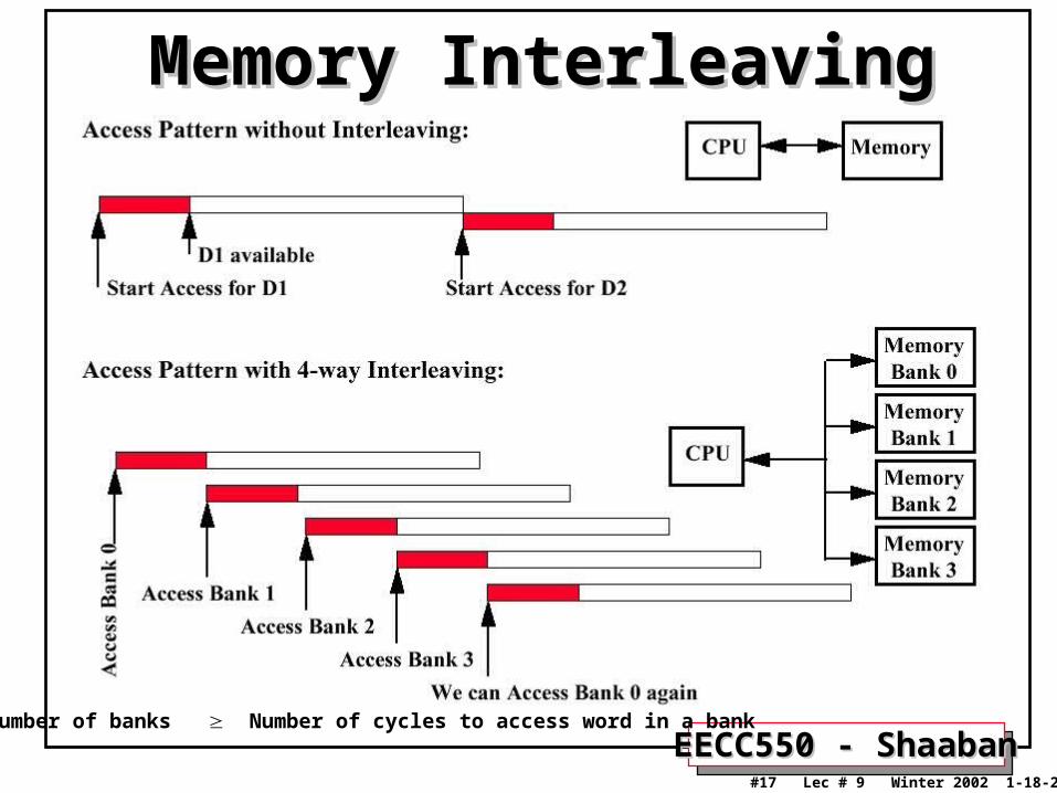
• Simple Interleaved Memory: Memory is organized as a number of banks each one word wide.
– Simultaneous multiple word memory reads or writes are accomplished by sending memory addresses to several memory banks at once.
– Interleaving factor: Refers to the mapping of memory addressees to memory banks.
e.g. using 4 banks, bank 0 has all words whose address is:
(word address mod) 4 = 0

EECC550 - ShaabanEECC550 - Shaaban#16 Lec # 9 Winter 2002 1-18-2003
Three examples of bus width, memory width, and memory interleaving to achieve higher memory bandwidth
Narrow busand cachewithinterleaved memory
Wider memory, busand cache
Simplest design:Everything is the width of one word
EECC550 - ShaabanEECC550 - Shaaban#17 Lec # 9 Winter 2002 1-18-2003
Memory InterleavingMemory Interleaving
Number of banks Number of cycles to access word in a bank

EECC550 - ShaabanEECC550 - Shaaban#18 Lec # 9 Winter 2002 1-18-2003
SynchronousSynchronousDynamic RAMDynamic RAM(SDRAM)(SDRAM)OrganizationOrganization
DDR SDRAM organization is similar but four banks are used in each DDR SDRAM chip instead of two.
Data transfer on both rising and falling edges of the clock.
DDR SDRAM rated by maximum memory bandwidthPC1600 = 8 bytes x 100 Mhz x 2 = 1600 Mbytes/sec
SDRAM speed is rated at max.clock speed supported:66MHZ = PC66100MHZ = PC100133MHZ = PC133

EECC550 - ShaabanEECC550 - Shaaban#19 Lec # 9 Winter 2002 1-18-2003
Simplified SDRAM Read TimingSimplified SDRAM Read Timing
Typical timing at 133 MHZ (PC133 SDRAM) : 5-1-1-1For bus width = 64 bits = 8 bytes Max. Bandwidth = 133 x 8 = 1064 Mbytes/secIt takes = 5+1+1+1 = 8 memory cycles or 7.5 ns x 8 = 60 ns to read 32 byte cache blockMinimum Read Miss penalty for CPU running at 1 GHZ = 7.5 x 8 = 60 CPU cycles

EECC550 - ShaabanEECC550 - Shaaban#20 Lec # 9 Winter 2002 1-18-2003
Four way interleaved memory
Three memory banks address interleaving : Sequentially interleaved addresses on the left, address requires a divisionRight: Alternate interleaving requires only modulo to a power of 2

EECC550 - ShaabanEECC550 - Shaaban#21 Lec # 9 Winter 2002 1-18-2003
Current Synchronous DRAM Interface Characteristics Summary
SDRAM
# of Banks per DRAM Chip
2 4 4? 32
EECC550 - ShaabanEECC550 - Shaaban#22 Lec # 9 Winter 2002 1-18-2003
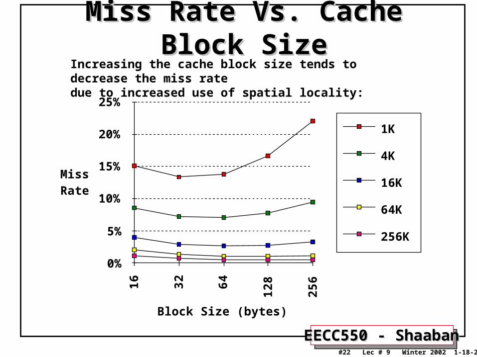
Miss Rate Vs. Cache Block SizeMiss Rate Vs. Cache Block SizeIncreasing the cache block size tends to decrease the miss ratedue to increased use of spatial locality:
Block Size (bytes)
Miss Rate
0%
5%
10%
15%
20%
25%
16
32
64
12
8
25
6
1K
4K
16K
64K
256K

EECC550 - ShaabanEECC550 - Shaaban#23 Lec # 9 Winter 2002 1-18-2003
Memory Width, Interleaving: An ExampleMemory Width, Interleaving: An ExampleGiven the following system parameters with single cache level L1:Block size=1 word Memory bus width=1 word Miss rate =3% Miss penalty=32 cycles
(4 cycles to send address 24 cycles access time/word, 4 cycles to send a word)
Memory access/instruction = 1.2 Ideal CPI (ignoring cache misses) = 2
Miss rate (block size=2 word)=2% Miss rate (block size=4 words) =1%
• The CPI of the base machine with 1-word blocks = 2+(1.2 x 0.03 x 32) = 3.15
• Increasing the block size to two words gives the following CPI:
– 32-bit bus and memory, no interleaving = 2 + (1.2 x .02 x 2 x 32) = 3.54
– 32-bit bus and memory, interleaved = 2 + (1.2 x .02 x (4 + 24 + 8) = 2.86
– 64-bit bus and memory, no interleaving = 2 + (1.2 x 0.02 x 1 x 32) = 2.77
• Increasing the block size to four words; resulting CPI:
– 32-bit bus and memory, no interleaving = 2 + (1.2 x 0.01 x 4 x 32) = 3.54
– 32-bit bus and memory, interleaved = 2 + (1.2 x 0.01 x (4 +24 + 16) = 2.53
– 64-bit bus and memory, no interleaving = 2 + (1.2 x 0.01 x 2 x 32) = 2.77
EECC550 - ShaabanEECC550 - Shaaban#24 Lec # 9 Winter 2002 1-18-2003
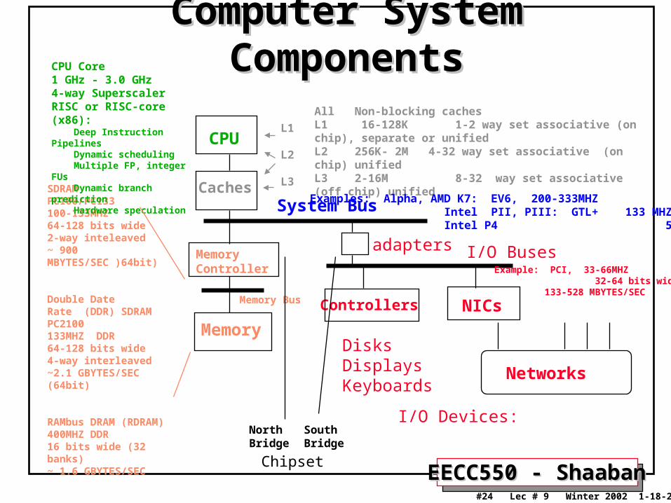
Computer System ComponentsComputer System Components
SDRAMPC100/PC133100-133MHZ64-128 bits wide2-way inteleaved~ 900 MBYTES/SEC )64bit)
Double DateRate (DDR) SDRAMPC2100133MHZ DDR64-128 bits wide4-way interleaved~2.1 GBYTES/SEC (64bit)
RAMbus DRAM (RDRAM)400MHZ DDR16 bits wide (32 banks)~ 1.6 GBYTES/SEC
CPU
CachesSystem Bus
I/O Devices:
Memory
Controllers
adapters
DisksDisplaysKeyboards
Networks
NICs
I/O BusesMemoryController Example: PCI, 33-66MHZ
32-64 bits wide 133-528 MBYTES/SEC
CPU Core1 GHz - 3.0 GHz4-way SuperscalerRISC or RISC-core (x86): Deep Instruction Pipelines Dynamic scheduling Multiple FP, integer FUs Dynamic branch prediction Hardware speculation
L1
L2 L3
Memory Bus
All Non-blocking cachesL1 16-128K 1-2 way set associative (on chip), separate or unifiedL2 256K- 2M 4-32 way set associative (on chip) unifiedL3 2-16M 8-32 way set associative (off chip) unified
Examples: Alpha, AMD K7: EV6, 200-333MHZ Intel PII, PIII: GTL+ 133 MHZ Intel P4 533 MHZ
NorthBridge
SouthBridge
Chipset

EECC550 - ShaabanEECC550 - Shaaban#25 Lec # 9 Winter 2002 1-18-2003
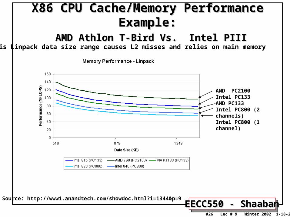
X86 CPU Cache/Memory Performance ExampleX86 CPU Cache/Memory Performance ExampleAMD Athlon T-Bird Vs. Intel PIIIAMD Athlon T-Bird Vs. Intel PIII
AMD Athlon T-Bird 1GHZL1: 64K INST, 64K DATA (3 cycle latency), both 2-wayL2: 256K 16-way 64 bit bus Latency: 7 cycles L1,L2 on-chip
Intel PIII GHZL1: 16K INST, 16K DATA (3 cycle latency), both 2-wayL2: 256K 8-way 256 bit , Latency: 7 cycles
L1,L2 on-chip (32 byte blocks)
Main Memory:
PC2100133MHZ DDR SDRAM 64bitPeak bandwidth: 2100 MB/sLatency Range: 19ns - 64ns
PC133133MHZ SDRAM 64bitPeak bandwidth: 1000 MB/sLatency Range: 25ns - 80ns
PC800Rambus DRDRAM400 MHZ DDR 16-bitPeak bandwidth: 1600 MB/s (1 channel)Latency Range: 35ns - 80ns
Intel 840 uses two PC800 channels Source: http://www1.anandtech.com/showdoc.html?i=1344&p=9
L1 HitL1 MissL2 Hit
L1 MissL2 Miss
64K320K
EECC550 - ShaabanEECC550 - Shaaban#26 Lec # 9 Winter 2002 1-18-2003
X86 CPU Cache/Memory Performance Example:X86 CPU Cache/Memory Performance Example: AMD Athlon T-Bird Vs. Intel PIIIAMD Athlon T-Bird Vs. Intel PIII
AMD PC2100Intel PC133AMD PC133Intel PC800 (2 channels)Intel PC800 (1 channel)
This Linpack data size range causes L2 misses and relies on main memory
Source: http://www1.anandtech.com/showdoc.html?i=1344&p=9

EECC550 - ShaabanEECC550 - Shaaban#27 Lec # 9 Winter 2002 1-18-2003
X86 CPU Cache/Memory Performance Example:X86 CPU Cache/Memory Performance Example:AMD Athlon T-Bird Vs. Intel PIII, Vs. P4AMD Athlon T-Bird Vs. Intel PIII, Vs. P4
AMD Athlon T-Bird 1GHZL1: 64K INST, 64K DATA (3 cycle latency), both 2-way L2: 256K 16-way 64 bit bus Latency: 7 cycles L1,L2 on-chip
Intel PIII 1 GHZL1: 16K INST, 16K DATA (3 cycle latency) both 2-way 32 byte blocksL2: 256K 8-way 256 bit bus , Latency: 7 cycles
L1,L2 on-chip
Intel P 4, 1.5 GHZL1: 8K DATA (2 cycle latency) 4-way 64 byte blocks 96KB Execution Trace CacheL2: 256K 8-way 256 bit bus , 128 byte blocks Latency: 7 cycles
L1,L2 on-chip
Source: http://www1.anandtech.com/showdoc.html?i=1360&p=15
EECC550 - ShaabanEECC550 - Shaaban#28 Lec # 9 Winter 2002 1-18-2003
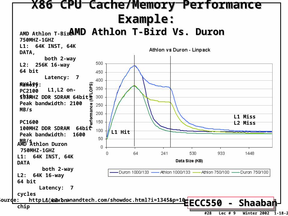
X86 CPU Cache/Memory Performance Example:X86 CPU Cache/Memory Performance Example:AMD Athlon T-Bird Vs. DuronAMD Athlon T-Bird Vs. Duron
AMD Athlon T-Bird 750MHZ-1GHZL1: 64K INST, 64K DATA, both 2-wayL2: 256K 16-way 64 bit Latency: 7 cycles L1,L2 on-chip
AMD Athlon Duron 750MHZ-1GHZL1: 64K INST, 64K DATA both 2-wayL2: 64K 16-way 64 bit Latency: 7 cycles L1,L2 on-chip
Source: http://www1.anandtech.com/showdoc.html?i=1345&p=10
Memory:PC2100133MHZ DDR SDRAM 64bitPeak bandwidth: 2100 MB/s
PC1600100MHZ DDR SDRAM 64bitPeak bandwidth: 1600 MB/s
L1 MissL2 Miss
L1 Hit

EECC550 - ShaabanEECC550 - Shaaban#29 Lec # 9 Winter 2002 1-18-2003
A Typical Memory HierarchyA Typical Memory Hierarchy
Control
Datapath
VirtualMemory,
SecondaryStorage(Disk)
Processor
Registers
MainMemory(DRAM)
SecondLevelCache
(SRAM)L2
1s 10,000,000s
(10s ms)
Speed (ns): 10s 100s
100s GsSize (bytes): Ks Ms
TertiaryStorage(Tape)
10,000,000,000s (10s sec)
Ts
On-ChipLevel OneCache L1
Larger CapacityFaster

EECC550 - ShaabanEECC550 - Shaaban#30 Lec # 9 Winter 2002 1-18-2003
Virtual MemoryVirtual Memory• Virtual memory controls two levels of the memory hierarchy:
• Main memory (DRAM).
• Mass storage (usually magnetic disks).
• Main memory is divided into blocks allocated to different running processes in the system:
• Fixed size blocks: Pages (size 4k to 64k bytes).
• Variable size blocks: Segments (largest size 216 up to 232).
• At any given time, for any running process, a portion of its data/code is
loaded in main memory while the rest is available only in mass storage. • A program code/data block needed for process execution and not present in
main memory result in a page fault (address fault) and the block has to be loaded into main main memory from disk.
• A program can be run in any location in main memory or disk by using a relocation mechanism controlled by the operating system which maps the address from virtual address space (logical program address) to physical address space (main memory, disk).

EECC550 - ShaabanEECC550 - Shaaban#31 Lec # 9 Winter 2002 1-18-2003
– Illusion of having more physical main memory
– Allows program relocation
– Protection from illegal memory access
Virtual MemoryVirtual MemoryBenefitsBenefits
3 2 1 01 1 1 0 9 81 5 1 4 1 3 1 23 1 3 0 2 9 2 8 2 7
Page offsetVirtual page number
Virtual address
3 2 1 01 1 1 0 9 81 5 1 4 1 3 1 22 9 2 8 2 7
Page offsetPhysical page number
Physical address
Translation

EECC550 - ShaabanEECC550 - Shaaban#32 Lec # 9 Winter 2002 1-18-2003
Paging Versus SegmentationPaging Versus Segmentation

EECC550 - ShaabanEECC550 - Shaaban#33 Lec # 9 Winter 2002 1-18-2003
Physical location of blocks A, B, C(allocated in memory by operating system)
Contiguous virtual addressspace of a program
Virtual Virtual Physical Address TranslationPhysical Address Translation
Page Fault: D in Disk(not allocated in main memory)

EECC550 - ShaabanEECC550 - Shaaban#34 Lec # 9 Winter 2002 1-18-2003
Mapping Virtual Addresses to Physical Mapping Virtual Addresses to Physical Addresses Using A Page TableAddresses Using A Page Table

EECC550 - ShaabanEECC550 - Shaaban#35 Lec # 9 Winter 2002 1-18-2003
Virtual Address TranslationVirtual Address Translation
Physical memory
Disk storage
Valid
1
1
1
1
0
1
1
0
1
1
0
1
Page table
Virtual page
number
Physica l page or
disk address
Pages allocated in main memory by operating system
Pages not allocated yet in main memory by operating system: Page Faults

EECC550 - ShaabanEECC550 - Shaaban#36 Lec # 9 Winter 2002 1-18-2003
Page Table OrganizationPage Table Organization
Page offsetVirtual page number
Virtual address
Page offsetPhysical page number
Physical address
Physical page numberV a lid
If 0 then page is notpresent in memory
Page table register
Page table
2 0 1 2
18
3 1 30 2 9 2 8 2 7 1 5 1 4 1 3 12 1 1 1 0 9 8 3 2 1 0
2 9 2 8 2 7 1 5 1 4 1 3 1 2 1 1 1 0 9 8 3 2 1 0
Two memory accesses needed:
• First to page table.• Second to item.

EECC550 - ShaabanEECC550 - Shaaban#37 Lec # 9 Winter 2002 1-18-2003
Typical Parameter Range For Typical Parameter Range For Cache & Virtual MemoryCache & Virtual Memory

EECC550 - ShaabanEECC550 - Shaaban#38 Lec # 9 Winter 2002 1-18-2003
Virtual Memory Issues/StrategiesVirtual Memory Issues/Strategies• Main memory block placement: Fully associative placement is used
to lower the miss rate.
• Block replacement: The least recently used (LRU) block is replaced when a new block is brought into main memory from disk.
• Write strategy: Write back is used and only those pages changed in main memory are written to disk (dirty bit scheme is used).
• To locate blocks in main memory a page table is utilized. The page table is indexed by the virtual page number and contains the physical address of the block.
– In paging: Offset is concatenated to this physical page address.
– In segmentation: Offset is added to the physical segment address.
• To limit the size of the page table to the number of physical pages in main memory a hashing scheme is used.
• Utilizing address locality, a translation look-aside buffer (TLB) is usually used to cache recent address translations and prevent a second memory access to read the page table.

EECC550 - ShaabanEECC550 - Shaaban#39 Lec # 9 Winter 2002 1-18-2003
Speeding Up Address Translation:Speeding Up Address Translation:
Translation Lookaside Buffer (TLB)Translation Lookaside Buffer (TLB)• TLB: A small on-chip cache used for address translations.• If a virtual address is found in TLB (a TLB hit), the page table in main memory is not accessed.
1
1
1
1
0
1
1
0
1
1
0
1
1
1
1
1
0
1
Physical Memory
Disk Storage
TLB (on-chip)32-256 TLB Entries
Physical Page Address
Virtual Page Number
Page Table(in main memory)
Physical Pageor Disk Address
TagValid
Valid

EECC550 - ShaabanEECC550 - Shaaban#40 Lec # 9 Winter 2002 1-18-2003
Operation of The Alpha 21264 Data TLB Operation of The Alpha 21264 Data TLB (DTLB) During Address Translation(DTLB) During Address Translation
Virtual addressVirtual address
DTLB = 128 entriesDTLB = 128 entries
ProtectionProtectionPermissionsPermissions Valid bitValid bit
Address Space Address Space Number (ASN)Number (ASN)Identifies processIdentifies processsimilar to PIDsimilar to PID(no need to flush (no need to flush TLB on context TLB on context switch)switch)
EECC550 - ShaabanEECC550 - Shaaban#41 Lec # 9 Winter 2002 1-18-2003
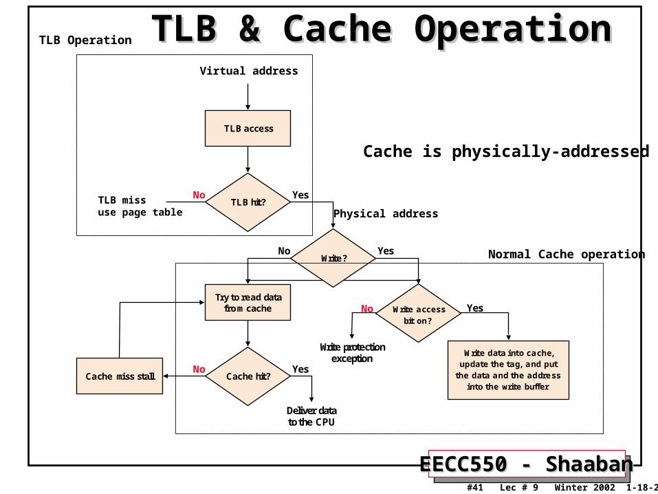
TLB & Cache OperationTLB & Cache Operation
Yes
Deliver datato the CPU
Write?
Try to read datafrom cache
W rite data into cache,update the tag, and put
the data and the addressinto the write buffer
Cache hit?Cache miss stall
TLB hit?
TLB access
No
YesNo
YesNo
W rite access
bit on?
YesNo
Write protectionexception
TLB missuse page table
Virtual address
Physical address
Normal Cache operation
Cache is physically-addressed
TLB Operation

EECC550 - ShaabanEECC550 - Shaaban#42 Lec # 9 Winter 2002 1-18-2003
CPU Performance with Real TLBsWhen a real TLB is used with a TLB miss rate and a TLB miss penalty is used:
CPI = CPIexecution + mem stalls per instruction + TLB stalls per instruction
Where:
Mem Stalls per instruction = Mem accesses per instruction x mem stalls per access
Similarly:
TLB Stalls per instruction = Mem accesses per instruction x TLB stalls per access
TLB stalls per access = TLB miss rate x TLB miss penalty
Example:
Given: CPIexecution = 1.3 Mem accesses per instruction = 1.4
Mem stalls per access = .5 TLB miss rate = .3% TLB miss penalty = 30 cycles
What is the reluting CPU CPI?
Mem Stalls per instruction = 1.4 x .5 = .7 cycles/instruction
TLB stalls per instruction = 1.4 x (TLB miss rate x TLB miss penalty)
= 1.4 x .003 x 30 = .126 cycles/instruction
CPI = 1. 3 + .7 + .126 = 2.126
EECC550 - ShaabanEECC550 - Shaaban#43 Lec # 9 Winter 2002 1-18-2003
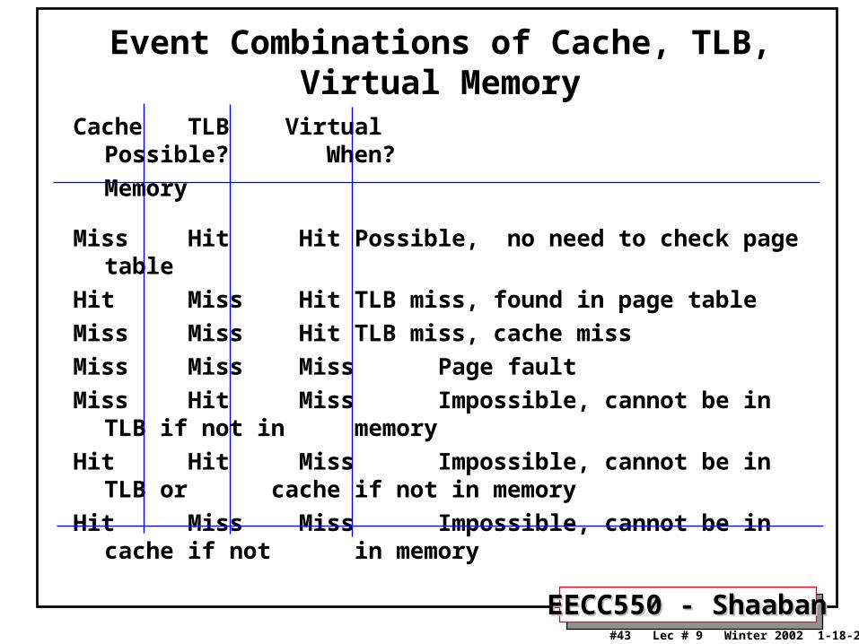
Event Combinations of Cache, TLB, Virtual Memory
Cache TLB Virtual Possible? When?
Memory
Miss Hit Hit Possible, no need to check page table
Hit Miss Hit TLB miss, found in page table
Miss Miss Hit TLB miss, cache miss
Miss Miss Miss Page fault
Miss Hit Miss Impossible, cannot be in TLB if not in memory
Hit Hit Miss Impossible, cannot be in TLB or cache if not in memory
Hit Miss Miss Impossible, cannot be in cache if not in memory