Embed Size (px)
Citation preview
EECE476
Lectures 10: Multi-cycle CPU Control
Chapter 5: Section 5.5
The University ofBritish Columbia EECE 476 © 2005 Guy Lemieux
2
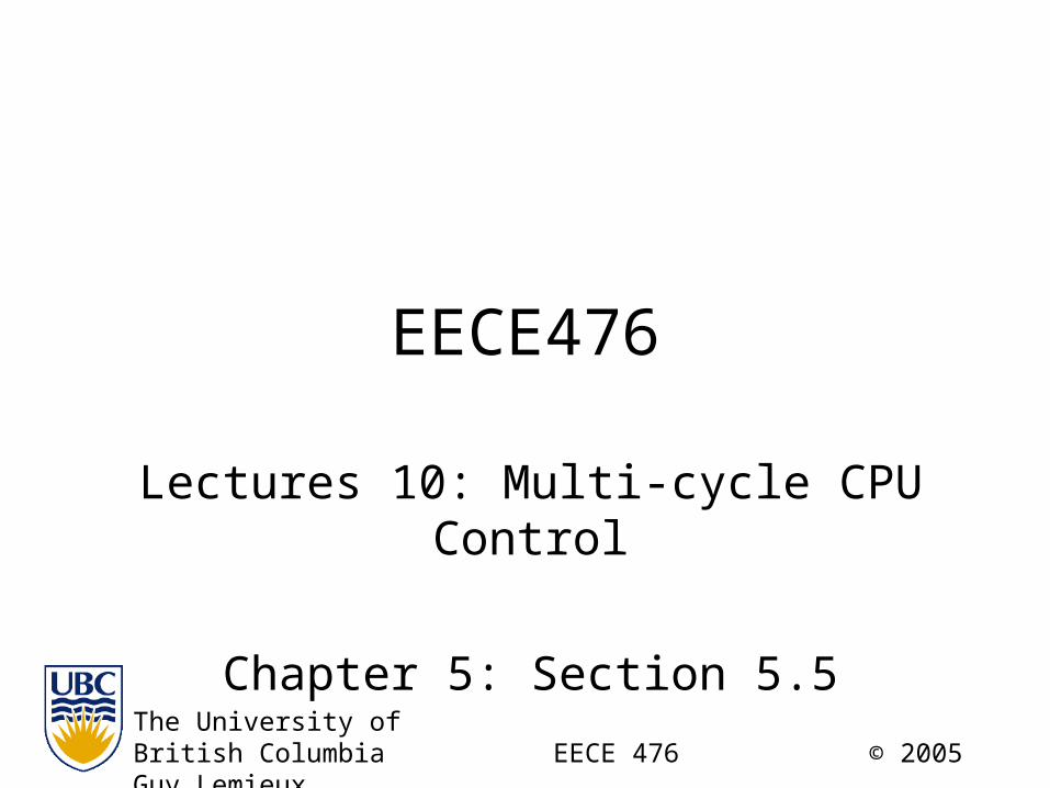
Multi-cycle BEQ Instruction
1. Fetch InstructionInstructionRegister ← Mem[PC]; PC ← PC + 4
2. Read Registers, Precompute TargetA ← Registers[Rs] ; B ← Registers[Rt] ; ALUOut ← PC + {SignExt{Imm16},b’00’}
3. Compare Registers, Conditional Branchif( (A – B) ==0 ) PC ← ALUOut
Green shows PC calculation flow (in parallel with other operations)
HOMEWORK FOR TOMORROWPrint out datapath diagram & ensure RTL is Valid !Determine control signal value for each cycle !!

3
Multi-cycle CPU Datapath+ Control Signals
Instr[25:21]
Instr[20:16]
Instr[15:0]
Instr[15:0]
Instruction[5:0]
In[15:11]
Instr[25:0]
PC[31..28]
Jumpaddress
[31..0]
PCWrite
IorDMemRead
MemWrite
MemtoReg
IRWritePCSrc
ALUOp
ALUSrcA
ALUSrcB
RegWrite
RegDst
ALUControl
4
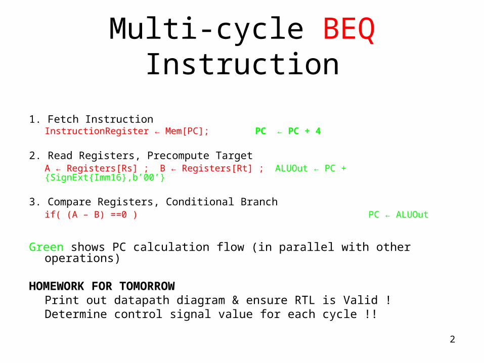
Multi-cycle CPU Datapath+ Controller
Instr.[31:26]
Instr[31:26]
Instr[25:21]
Instr[20:16]
Instr[15:0]
Instr[15:0]
Instruction[5:0]
In[15:11]
Instr[25:0]
PC[31..28]
Jumpaddress
[31..0]
5
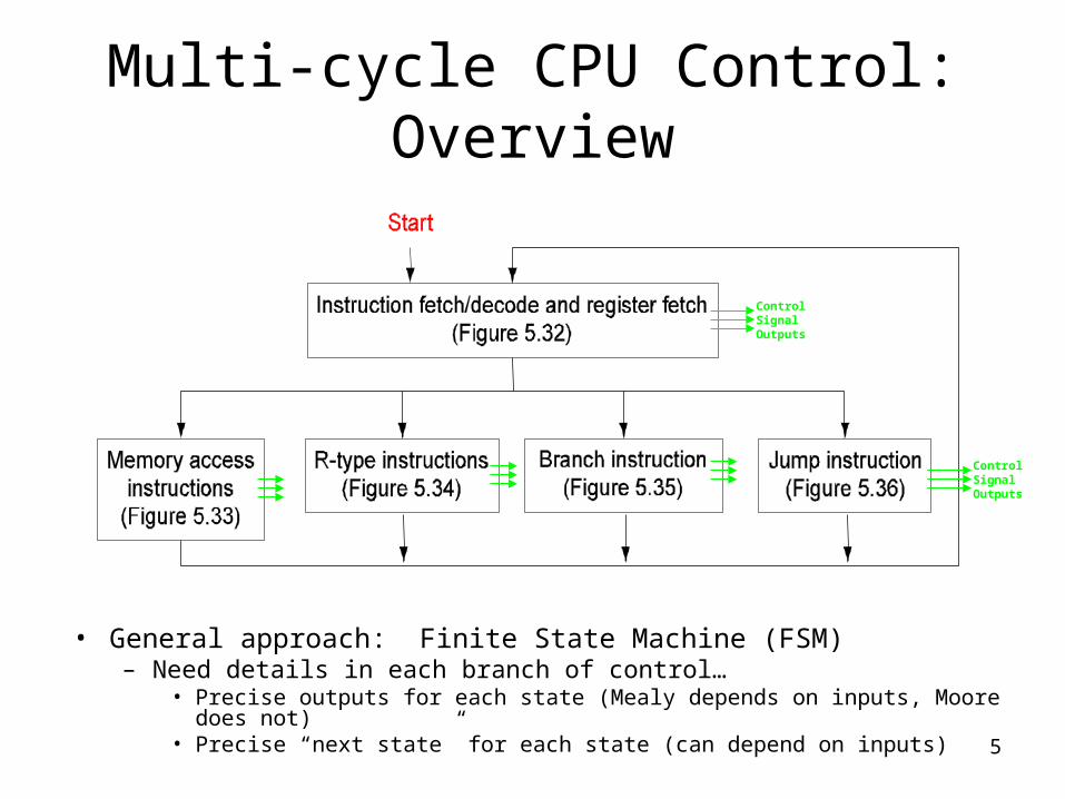
Multi-cycle CPU Control: Overview
• General approach: Finite State Machine (FSM)– Need details in each branch of control…
• Precise outputs for each state (Mealy depends on inputs, Moore does not)• Precise “next state” for each state (can depend on inputs)
ControlSignalOutputs
ControlSignalOutputs

6
How to Implement FSM ?• Manually with logic gates + FFs
– Bubble diagram, next-state table, state assignment– Karnaugh map for each state bit, each output bit (painful!)
• High-level language description (eg, Verilog, VHDL)– Describe FSM bubble diagram (next-states, output values)– Automatically synthesized into gates + FFs
• Microcode (µ-code) description– Sequence through many µ-ops for each CPU instruction
• One µ-op (µ-instruction) sends correct control signal for 1 cycle• µ-op similar to one bubble in FSM
– Acts like a mini-CPU within a CPU• µPC: microcode program counter• Microcode storage memory contains µ-ops
– Can look similar to RTL or some new “assembly language”

7
FSM Specification: Bubble Diagram
Can build thisby examiningRTL
It is possible toautomaticallyconvert RTLinto this form !

8
FSM: Gates + FFs Implementation
FSMHigh-level
Organization

9
FSM: Microcode Implementation
Adder
1
Datapathcontroloutputs
Sequencingcontrol
Inputs from instructionregister opcode field
MicrocodeStorage
(memory)
Inputs
Outputs
Microprogram Counter
Address Select Logic

10
Multi-cycle CPU:Datapath + Control FSM
Instr.[31:26]
Instr[31:26]
Instr[25:21]
Instr[20:16]
Instr[15:0]
Instr[15:0]
Instruction[5:0]
In[15:11]
Instr[25:0]
PC[31..28]
Jumpaddress
[31..0]
FSMControlOutputs
ConditionalBranch

11
Control FSM: Overview
• General approach: Finite State Machine (FSM)• Need details in each branch of control…

12
Detailed FSM
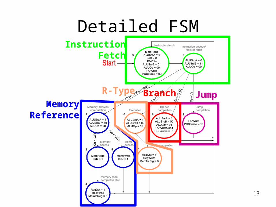
13
Detailed FSMInstruction
Fetch
MemoryReference
Branch JumpR-Type
14
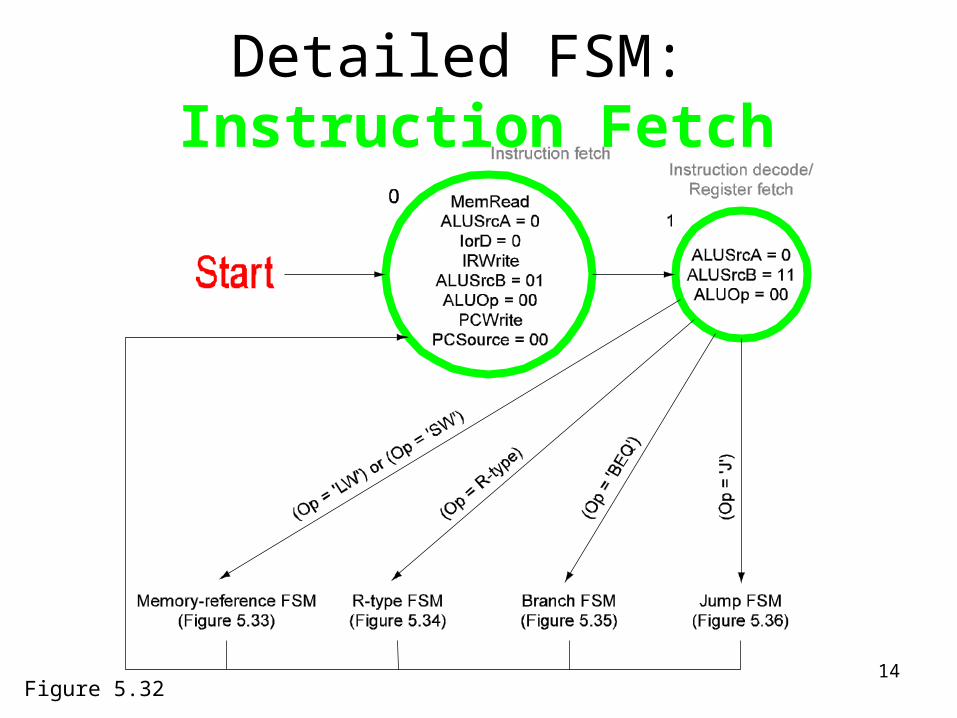
Detailed FSM: Instruction Fetch
Figure 5.32

15
Detailed FSM: Memory Reference
Figure 5.33
LW SW

16
Detailed FSM: R-Type Instruction
Figure 5.34

17
Detailed FSM: Branch Instruction
Figure 5.35
18
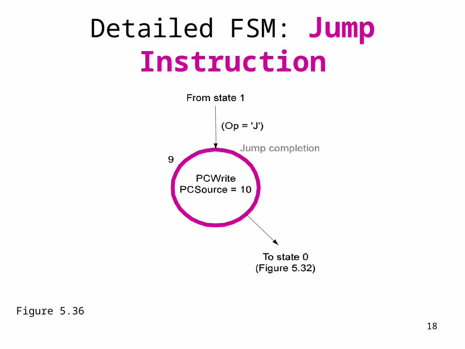
Detailed FSM: Jump Instruction
Figure 5.36

High-level Performance Comparison
Single-cycle CPU
vs
Multi-cycle CPU

20
Simple Comparison
Single-cycle CPU
1 clock cycle
5 clock cycles
Multi-cycle CPU
4 clock cycles
Multi-cycle CPU
3 clock cycles
Multi-cycle CPU
SW, R-type
BEQ, J
LW
All

21
What’s really happening?
Single-cycle CPU
Multi-cycle CPU
( Load Word Instruction )
Fetch Decode Memory WriteCalcAddr
Ideally:

22
In practise, steps differ in speeds…
Single-cycle CPU
Multi-cycle CPU
Fetch Decode MemoryCalcAddr
Fetch Decode MemoryCalcAddr
Write
Write
Violation!Wasted time!
Load Word Instruction

23
Single-cycle vs Multi-cycle
Single-cycle CPU
LW instruction faster for single-cycle
Fetch Decode MemoryCalcAddr
Fetch Decode MemoryCalcAddr
Write
Write
Violation fixed!
Multi-cycle CPU
Now wasted time is larger!

24
Single-cycle vs Multi-cycle
Single-cycle CPU
SW instruction ~ same speed
Fetch Decode MemoryCalcAddr
Fetch Decode MemoryCalcAddr
Multi-cycle CPU
Wasted time!
Speed diff

25
Single-cycle vs Multi-cycle
Single-cycle CPU
BEQ, J instruction faster for multi-cycle
Fetch DecodeCalcAddr
Fetch DecodeCalcAddr
Wasted time!
Speed diff
Multi-cycle CPU
26
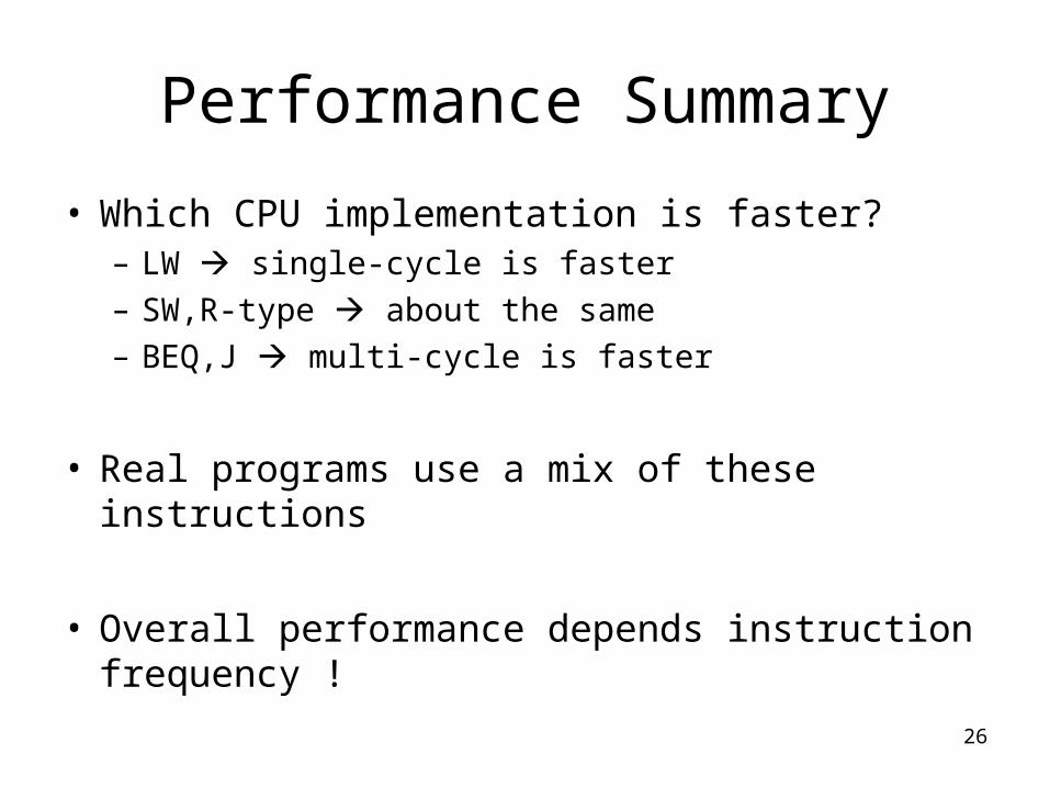
Performance Summary
• Which CPU implementation is faster?– LW single-cycle is faster– SW,R-type about the same– BEQ,J multi-cycle is faster
• Real programs use a mix of these instructions
• Overall performance depends instruction frequency !

27
Implementation Summary• Single-cycle CPU
– 1 instruction per cycle (eg, 1MHz 1 MIPS)– No “wasted time” on most complex instruction– Large wasted time on simpler instructions– Simple controller (just a lookup table or memory)– Simple instructions
• Multi-cycle CPU– << 1 instruction per cycle (eg, 1MHz 0.2 MIPS)– Small time wasted on most complex instruction
• Hence, this instruction always slower than single-cycle CPU– Small time wasted on simple instructions
• Eliminates “large wasted time” by using fewer clock cycles– Complex controller (FSM)– Potential to create complex instructions