Embed Size (px)
Citation preview
1 SM EECE 488 – Set 1: Introduction and Background
EECE488: Analog CMOS Integrated Circuit Design
Introduction and Background
Shahriar Mirabbasi
Department of Electrical and Computer Engineering
University of British Columbia
Technical contributions of Pedram Lajevardi in revising the slides is greatly acknowledged.

2 SM EECE 488 – Set 1: Introduction and Background
Marking
Assignments
10% (4 to 6)
Midterm 15%
Project 25%
Final Exam 50%
3 SM EECE 488 – Set 1: Introduction and Background
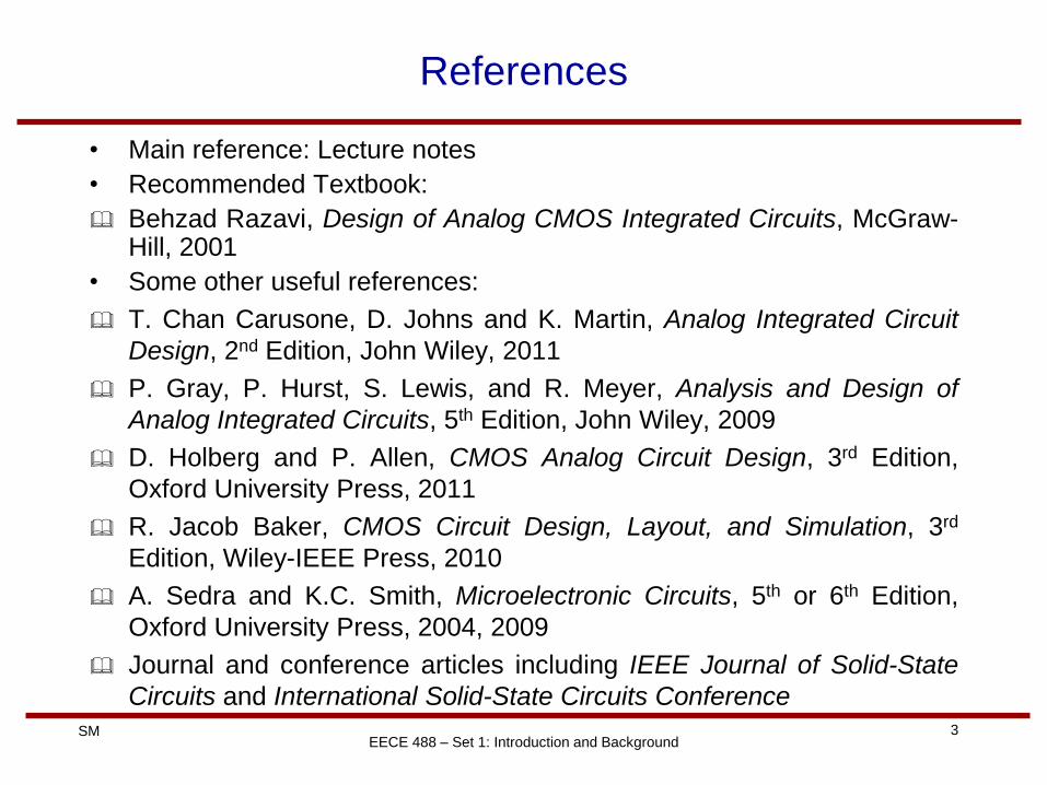
References
• Main reference: Lecture notes
• Recommended Textbook:
Behzad Razavi, Design of Analog CMOS Integrated Circuits, McGraw-Hill, 2001
• Some other useful references:
T. Chan Carusone, D. Johns and K. Martin, Analog Integrated Circuit
Design, 2nd Edition, John Wiley, 2011
P. Gray, P. Hurst, S. Lewis, and R. Meyer, Analysis and Design of
Analog Integrated Circuits, 5th Edition, John Wiley, 2009
D. Holberg and P. Allen, CMOS Analog Circuit Design, 3rd Edition,
Oxford University Press, 2011
R. Jacob Baker, CMOS Circuit Design, Layout, and Simulation, 3rd
Edition, Wiley-IEEE Press, 2010
A. Sedra and K.C. Smith, Microelectronic Circuits, 5th or 6th Edition,
Oxford University Press, 2004, 2009
Journal and conference articles including IEEE Journal of Solid-State
Circuits and International Solid-State Circuits Conference
4 SM EECE 488 – Set 1: Introduction and Background
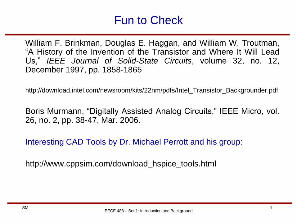
Fun to Check
William F. Brinkman, Douglas E. Haggan, and William W. Troutman, “A History of the Invention of the Transistor and Where It Will Lead Us,” IEEE Journal of Solid-State Circuits, volume 32, no. 12, December 1997, pp. 1858-1865
http://download.intel.com/newsroom/kits/22nm/pdfs/Intel_Transistor_Backgrounder.pdf
Boris Murmann, “Digitally Assisted Analog Circuits,” IEEE Micro, vol. 26, no. 2, pp. 38-47, Mar. 2006.
Interesting CAD Tools by Dr. Michael Perrott and his group:
http://www.cppsim.com/download_hspice_tools.html
5 SM EECE 488 – Set 1: Introduction and Background
Why Analog?
• Most of the physical signals are analog in nature!
• Although digital is great we need an analog interface to convert physical signals from analog to digital
• Also, in some application after processing the signals in digital domain, we need to convert them back to analog.
• Thus in many applications analog and mixed-signal circuits are the performance bottlenecks.
• Also with constant process improvements the boundary of between high-speed digital and analog circuits becomes more and more fuzzy!
• That is why analog and mixed-signal designers are still and hopefully will be in demand for the foreseeable future.
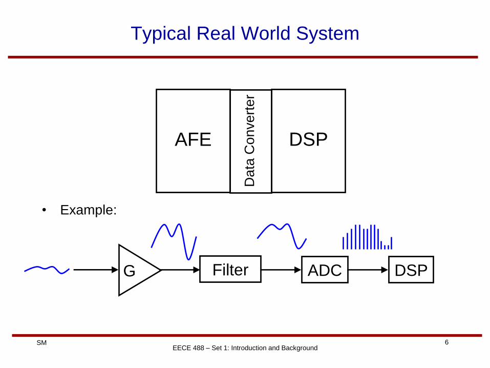
6 SM EECE 488 – Set 1: Introduction and Background
Typical Real World System
• Example:
DSP
Da
ta C
on
ve
rte
r
AFE
Filter ADC DSP G

7 SM
Intel’s Tick-Tock Model
EECE 488 – Set 1: Introduction and Background
Tick (process technology advancement), Tock (new microarchitecture)
http://www.intel.com/content/www/us/en/silicon-innovations/intel-tick-tock-model-general.html
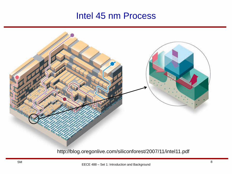
8 SM
Intel 45 nm Process
EECE 488 – Set 1: Introduction and Background
http://blog.oregonlive.com/siliconforest/2007/11/intel11.pdf
9 SM EECE 488 – Set 1: Introduction and Background
Background
1. Suggested Reading
2. Structure of MOS Transistors
3. Threshold Voltage
4. Long-Channel Current Equations
5. Regions of Operation
6. Transconductance
7. Second-Order Effects
8. Short-Channel Effects
9. MOS Layout
10.Device Capacitances
11.Small-signal Models
12.Circuit Impedance
13.Equivalent Transconductance
10 SM EECE 488 – Set 1: Introduction and Background
Suggested Reading
• Most of the material in this set are based on
Chapters 2, 16, and 17 of the Razavi’s book: Design of Analog
CMOS Integrated Circuits
Many of the figures in this set are from © Design of Analog CMOS Integrated Circuits,
McGraw-Hill, 2001, unless otherwise noted.
11 SM EECE 488 – Set 1: Introduction and Background
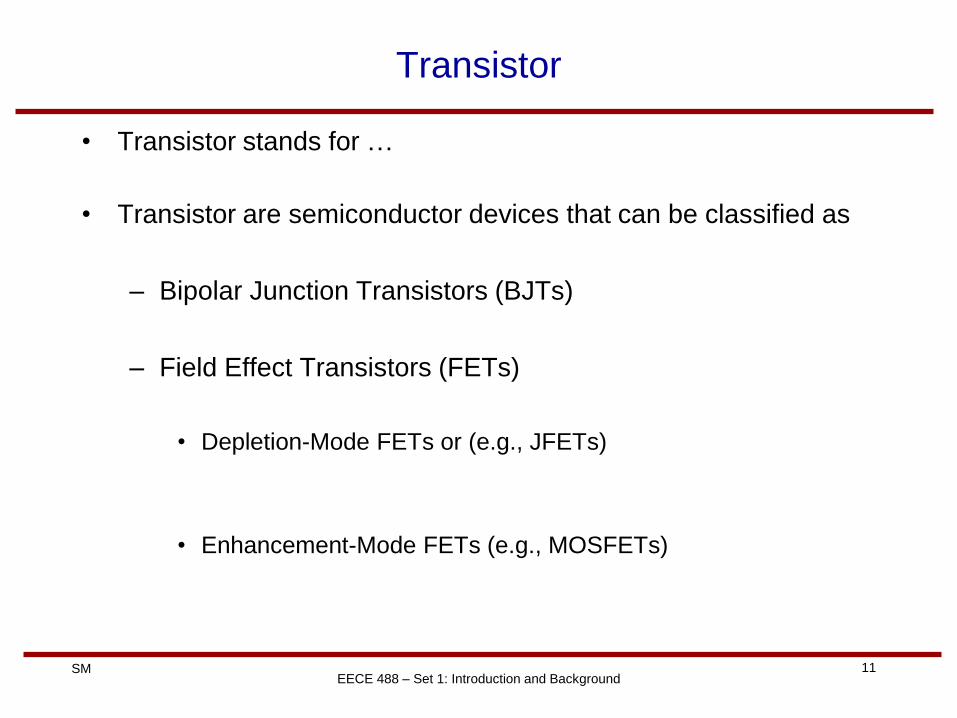
Transistor
• Transistor stands for …
• Transistor are semiconductor devices that can be classified as
– Bipolar Junction Transistors (BJTs)
– Field Effect Transistors (FETs)
• Depletion-Mode FETs or (e.g., JFETs)
• Enhancement-Mode FETs (e.g., MOSFETs)
12 SM EECE 488 – Set 1: Introduction and Background
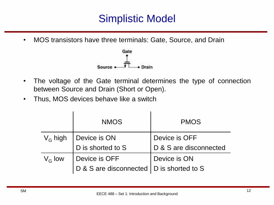
Simplistic Model
• MOS transistors have three terminals: Gate, Source, and Drain
• The voltage of the Gate terminal determines the type of connection
between Source and Drain (Short or Open).
• Thus, MOS devices behave like a switch
Device is ON
D is shorted to S
Device is OFF
D & S are disconnected
VG low
Device is OFF
D & S are disconnected
Device is ON
D is shorted to S
VG high
PMOS NMOS
13 SM EECE 488 – Set 1: Introduction and Background
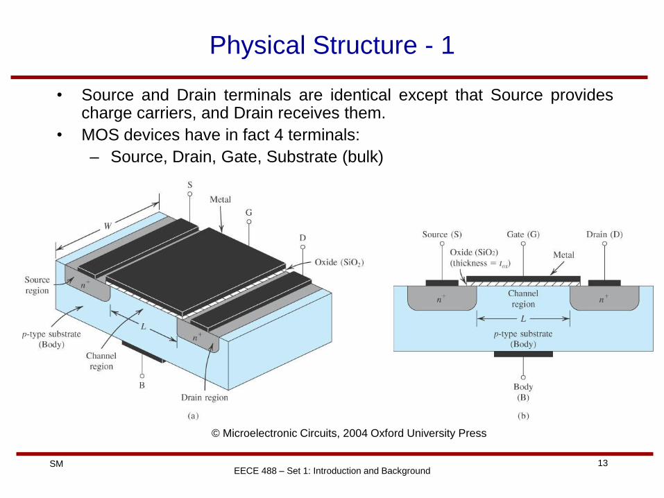
Physical Structure - 1
• Source and Drain terminals are identical except that Source provides charge carriers, and Drain receives them.
• MOS devices have in fact 4 terminals:
– Source, Drain, Gate, Substrate (bulk)
© Microelectronic Circuits, 2004 Oxford University Press
14 SM EECE 488 – Set 1: Introduction and Background
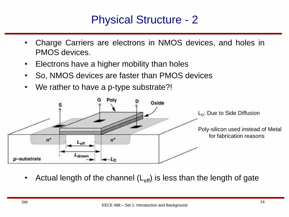
Physical Structure - 2
LD: Due to Side Diffusion
Poly-silicon used instead of Metal
for fabrication reasons
• Actual length of the channel (Leff) is less than the length of gate
• Charge Carriers are electrons in NMOS devices, and holes in
PMOS devices.
• Electrons have a higher mobility than holes
• So, NMOS devices are faster than PMOS devices
• We rather to have a p-type substrate?!
15 SM EECE 488 – Set 1: Introduction and Background
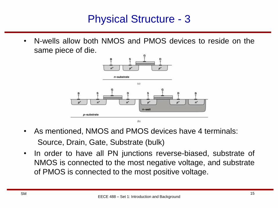
Physical Structure - 3
• N-wells allow both NMOS and PMOS devices to reside on the
same piece of die.
• As mentioned, NMOS and PMOS devices have 4 terminals:
Source, Drain, Gate, Substrate (bulk)
• In order to have all PN junctions reverse-biased, substrate of
NMOS is connected to the most negative voltage, and substrate
of PMOS is connected to the most positive voltage.
16 SM EECE 488 – Set 1: Introduction and Background
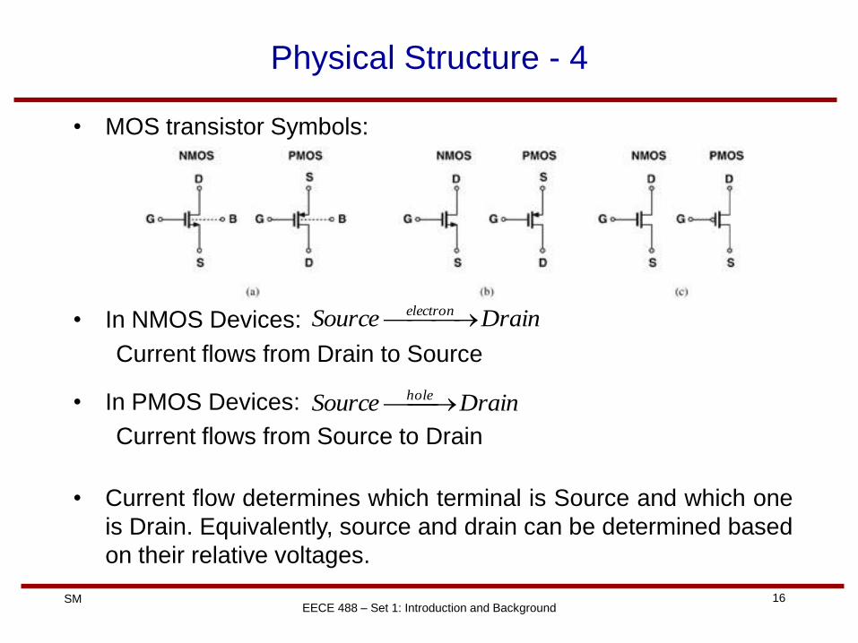
Physical Structure - 4
• MOS transistor Symbols:
• In NMOS Devices:
Current flows from Drain to Source
• In PMOS Devices:
Current flows from Source to Drain
• Current flow determines which terminal is Source and which one
is Drain. Equivalently, source and drain can be determined based
on their relative voltages.
DrainSource electron
DrainSource hole
17 SM EECE 488 – Set 1: Introduction and Background
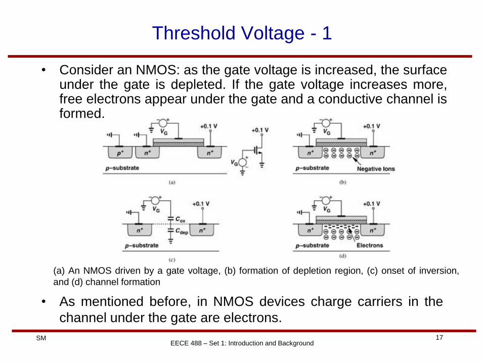
Threshold Voltage - 1
(a) An NMOS driven by a gate voltage, (b) formation of depletion region, (c) onset of inversion,
and (d) channel formation
• Consider an NMOS: as the gate voltage is increased, the surface under the gate is depleted. If the gate voltage increases more, free electrons appear under the gate and a conductive channel is formed.
• As mentioned before, in NMOS devices charge carriers in the
channel under the gate are electrons.
18 SM EECE 488 – Set 1: Introduction and Background
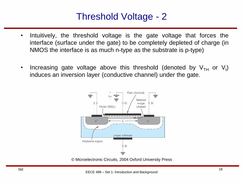
Threshold Voltage - 2
• Intuitively, the threshold voltage is the gate voltage that forces the
interface (surface under the gate) to be completely depleted of charge (in
NMOS the interface is as much n-type as the substrate is p-type)
• Increasing gate voltage above this threshold (denoted by VTH or Vt)
induces an inversion layer (conductive channel) under the gate.
© Microelectronic Circuits, 2004 Oxford University Press
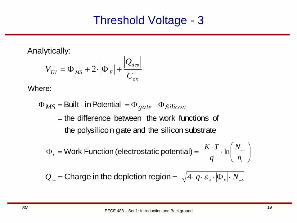
19 SM EECE 488 – Set 1: Introduction and Background
Threshold Voltage - 3
Analytically:
ox
dep
FMSTHC
QV 2
Where:
substrate silicon the and gate npolysilico the
of functions workthe between difference the
Potential in-Built
SilicongateMS
i
sub
F
n
N
q
TK lnpotential)atic (electrost Function Work
subFsidepNq Q 4region depletion the in Charge
20 SM EECE 488 – Set 1: Introduction and Background
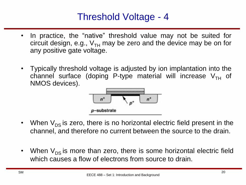
Threshold Voltage - 4
• In practice, the “native” threshold value may not be suited for circuit design, e.g., VTH may be zero and the device may be on for any positive gate voltage.
• Typically threshold voltage is adjusted by ion implantation into the channel surface (doping P-type material will increase VTH of NMOS devices).
• When VDS is zero, there is no horizontal electric field present in the
channel, and therefore no current between the source to the drain.
• When VDS is more than zero, there is some horizontal electric field
which causes a flow of electrons from source to drain.
21 SM EECE 488 – Set 1: Introduction and Background
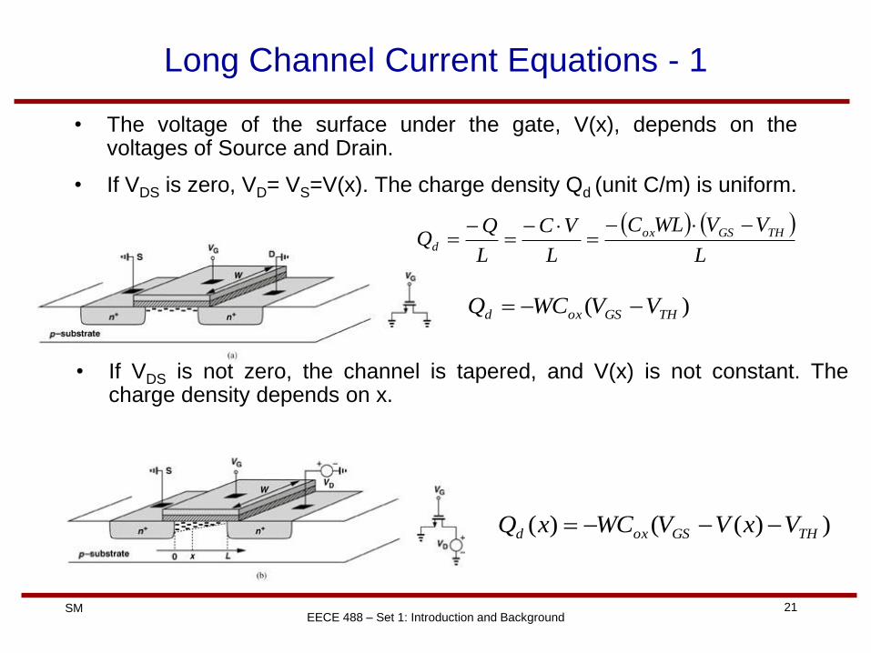
Long Channel Current Equations - 1
• The voltage of the surface under the gate, V(x), depends on the voltages of Source and Drain.
• If VDS is zero, VD= VS=V(x). The charge density Qd (unit C/m) is uniform.
)( THGSoxd VVWCQ
))(()( THGSoxd VxVVWCxQ
L
VVWLC
L
VC
L
QQ THGSox
d
• If VDS is not zero, the channel is tapered, and V(x) is not constant. The charge density depends on x.
22 SM EECE 488 – Set 1: Introduction and Background
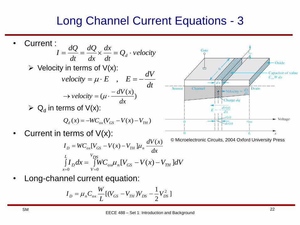
Long Channel Current Equations - 3
velocityQdt
dx
dx
dQ
dt
dQI d
dt
dVEEvelocity ,
))(
(dx
xdVvelocity
))(()( THGSoxd VxVVWCxQ
DSV
VTHGSnox
L
xD dVVxVVWCdxI
00
])([
]2
1)[( 2
DSDSTHGSoxnD VVVVL
WCI
• Current :
Velocity in terms of V(x):
Qd in terms of V(x):
dx
xdVVxVVWCI nTHGSoxD
)(])([
• Current in terms of V(x):
• Long-channel current equation:
© Microelectronic Circuits, 2004 Oxford University Press
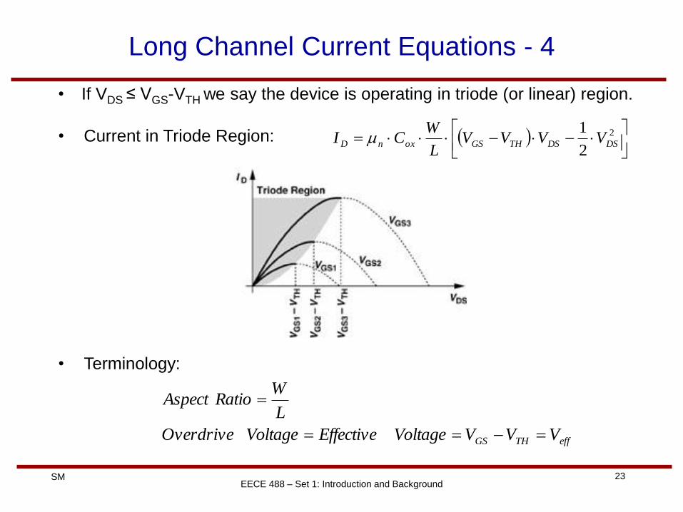
23 SM EECE 488 – Set 1: Introduction and Background
Long Channel Current Equations - 4
2
2
1DSDSTHGSoxnD VVVV
L
WCI
• Terminology:
effTHGS VVVVoltageEffectiveVoltageOverdrive
L
WRatioAspect
• Current in Triode Region:
• If VDS ≤ VGS-VTH we say the device is operating in triode (or linear) region.
24 SM EECE 488 – Set 1: Introduction and Background
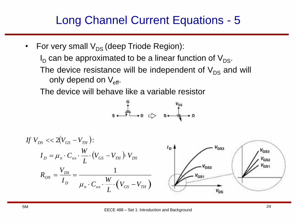
Long Channel Current Equations - 5
THGSoxnD
DSON
DSTHGSoxnD
THGSDS
VVL
WC
I
VR
VVVL
WCI
VVVIf
1
:2
• For very small VDS (deep Triode Region):
ID can be approximated to be a linear function of VDS.
The device resistance will be independent of VDS and will
only depend on Veff.
The device will behave like a variable resistor
25 SM EECE 488 – Set 1: Introduction and Background
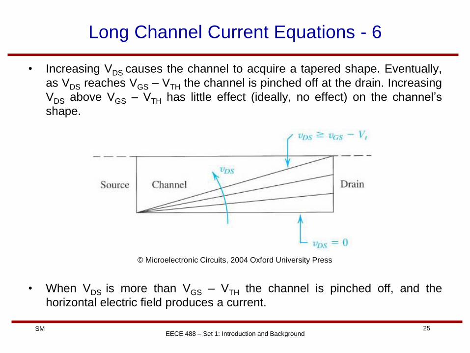
Long Channel Current Equations - 6
• Increasing VDS causes the channel to acquire a tapered shape. Eventually,
as VDS reaches VGS – VTH the channel is pinched off at the drain. Increasing
VDS above VGS – VTH has little effect (ideally, no effect) on the channel’s
shape.
© Microelectronic Circuits, 2004 Oxford University Press
• When VDS is more than VGS – VTH the channel is pinched off, and the
horizontal electric field produces a current.
26 SM EECE 488 – Set 1: Introduction and Background
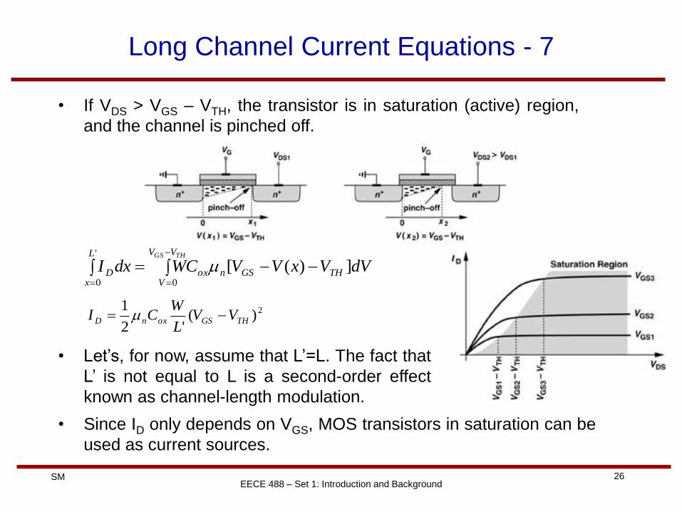
Long Channel Current Equations - 7
• If VDS > VGS – VTH, the transistor is in saturation (active) region,
and the channel is pinched off.
THGS VV
VTHGSnox
L
xD dVVxVVWCdxI
0
'
0
])([
2)('2
1THGSoxnD VV
L
WCI
• Let’s, for now, assume that L’=L. The fact that
L’ is not equal to L is a second-order effect
known as channel-length modulation.
• Since ID only depends on VGS, MOS transistors in saturation can be
used as current sources.
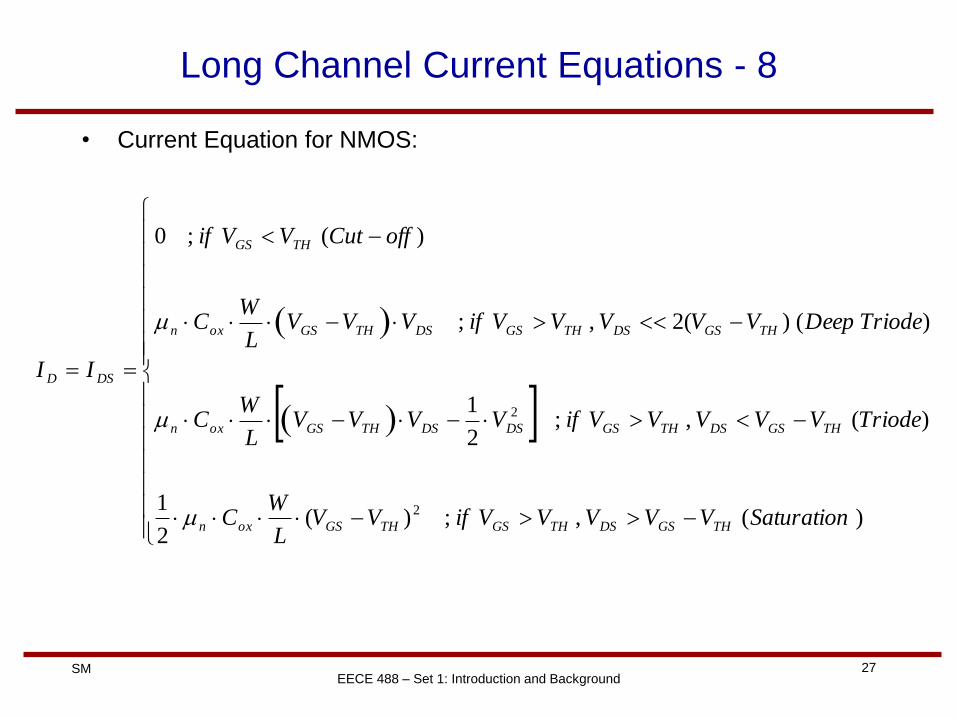
27 SM EECE 488 – Set 1: Introduction and Background
Long Channel Current Equations - 8
• Current Equation for NMOS:
)(,;)(2
1
)(,;2
1
)()(2,;
)(;0
2
2
SaturationVVVVVifVVL
WC
TriodeVVVVVifVVVVL
WC
TriodeDeepVVVVVifVVVL
WC
offCutVVif
II
THGSDSTHGSTHGSoxn
THGSDSTHGSDSDSTHGSoxn
THGSDSTHGSDSTHGSoxn
THGS
DSD
28 SM EECE 488 – Set 1: Introduction and Background
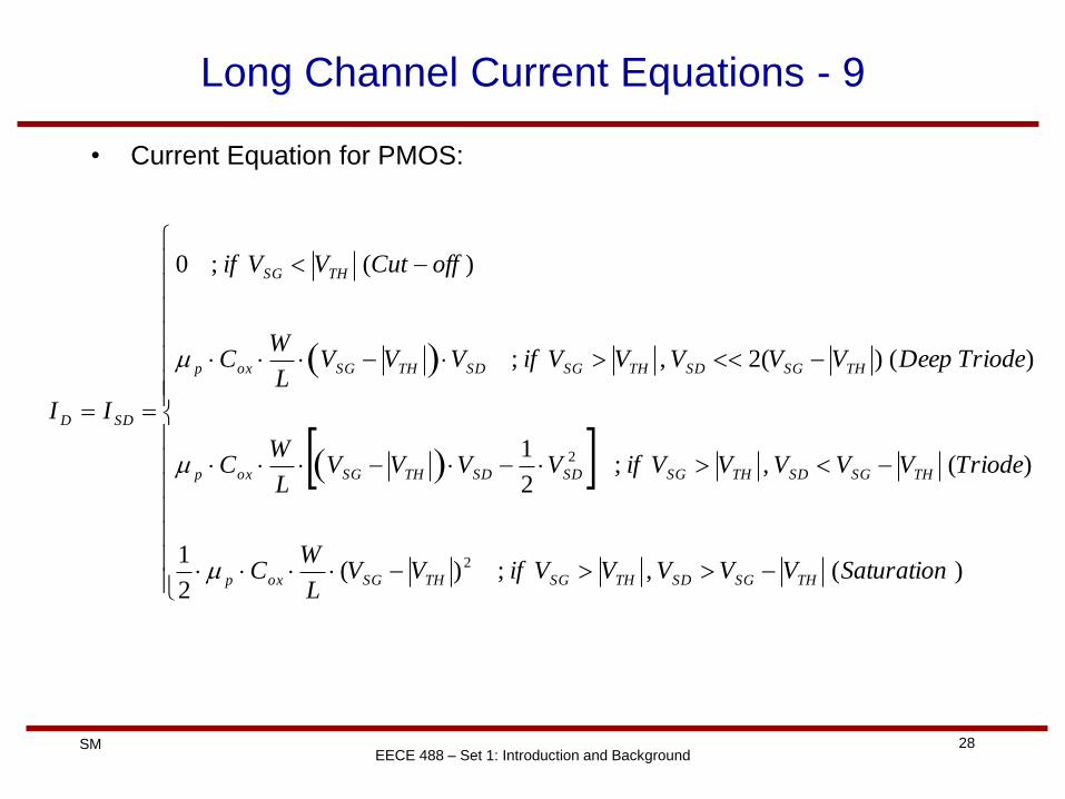
Long Channel Current Equations - 9
• Current Equation for PMOS:
)(,;)(2
1
)(,;2
1
)()(2,;
)(;0
2
2
SaturationVVVVVifVVL
WC
TriodeVVVVVifVVVVL
WC
TriodeDeepVVVVVifVVVL
WC
offCutVVif
II
THSGSDTHSGTHSGoxp
THSGSDTHSGSDSDTHSGoxp
THSGSDTHSGSDTHSGoxp
THSG
SDD
29 SM EECE 488 – Set 1: Introduction and Background
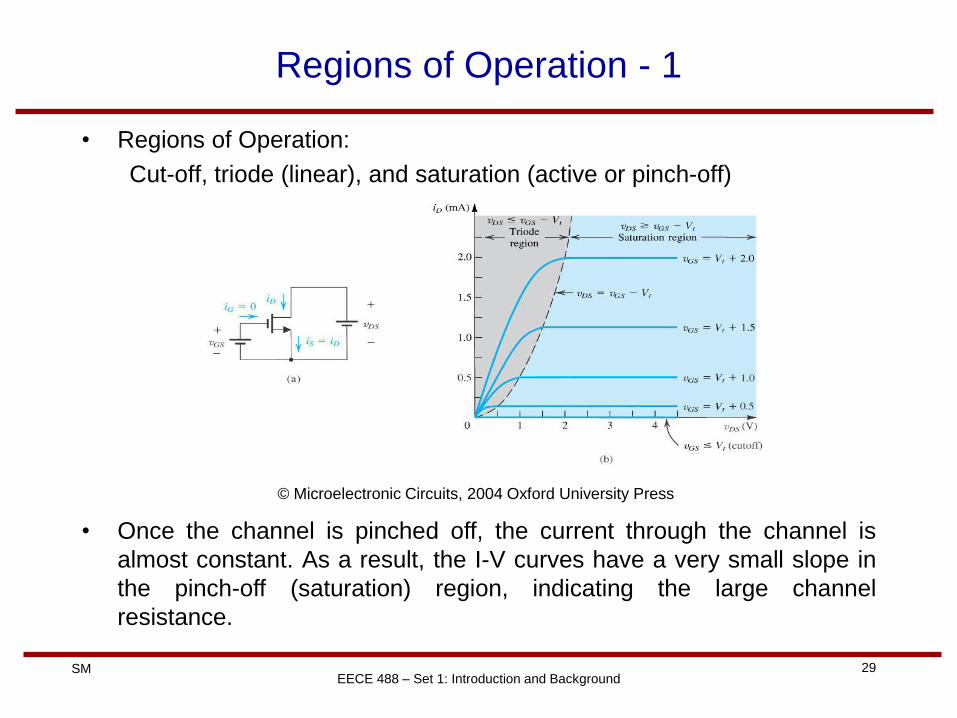
Regions of Operation - 1
• Regions of Operation:
Cut-off, triode (linear), and saturation (active or pinch-off)
© Microelectronic Circuits, 2004 Oxford University Press
• Once the channel is pinched off, the current through the channel is
almost constant. As a result, the I-V curves have a very small slope in
the pinch-off (saturation) region, indicating the large channel
resistance.
30 SM EECE 488 – Set 1: Introduction and Background
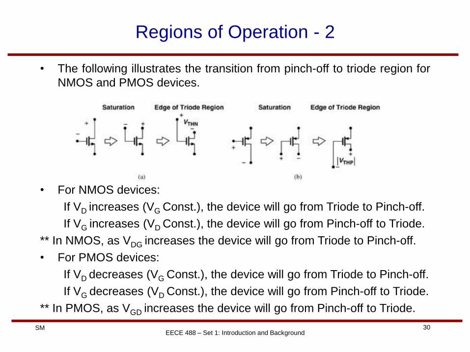
Regions of Operation - 2
• The following illustrates the transition from pinch-off to triode region for
NMOS and PMOS devices.
• For NMOS devices:
If VD increases (VG Const.), the device will go from Triode to Pinch-off.
If VG increases (VD Const.), the device will go from Pinch-off to Triode.
** In NMOS, as VDG increases the device will go from Triode to Pinch-off.
• For PMOS devices:
If VD decreases (VG Const.), the device will go from Triode to Pinch-off.
If VG decreases (VD Const.), the device will go from Pinch-off to Triode.
** In PMOS, as VGD increases the device will go from Pinch-off to Triode.
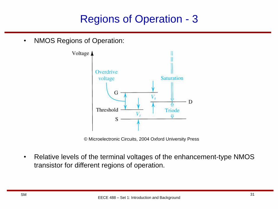
31 SM EECE 488 – Set 1: Introduction and Background
Regions of Operation - 3
© Microelectronic Circuits, 2004 Oxford University Press
• NMOS Regions of Operation:
• Relative levels of the terminal voltages of the enhancement-type NMOS
transistor for different regions of operation.
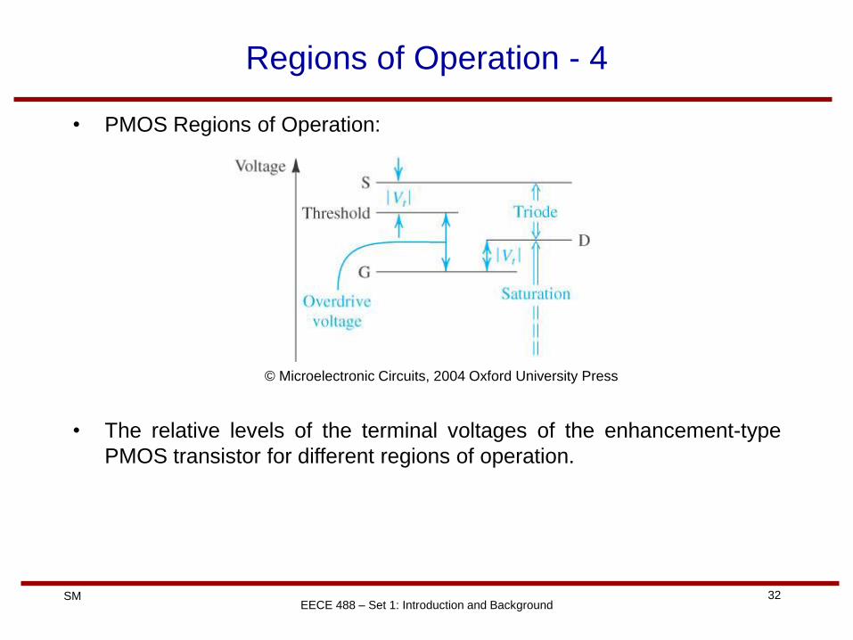
32 SM EECE 488 – Set 1: Introduction and Background
Regions of Operation - 4
© Microelectronic Circuits, 2004 Oxford University Press
• PMOS Regions of Operation:
• The relative levels of the terminal voltages of the enhancement-type
PMOS transistor for different regions of operation.
33 SM EECE 488 – Set 1: Introduction and Background
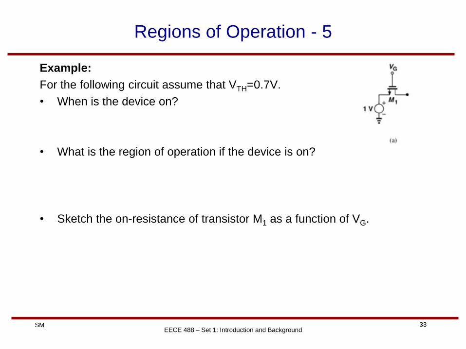
Regions of Operation - 5
Example:
For the following circuit assume that VTH=0.7V.
• When is the device on?
• What is the region of operation if the device is on?
• Sketch the on-resistance of transistor M1 as a function of VG.
34 SM EECE 488 – Set 1: Introduction and Background
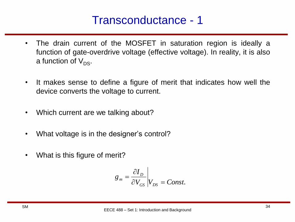
Transconductance - 1
• The drain current of the MOSFET in saturation region is ideally a
function of gate-overdrive voltage (effective voltage). In reality, it is also
a function of VDS.
• It makes sense to define a figure of merit that indicates how well the
device converts the voltage to current.
• Which current are we talking about?
• What voltage is in the designer’s control?
• What is this figure of merit?
.ConstVV
Ig
DSGS
Dm
35 SM EECE 488 – Set 1: Introduction and Background
Transconductance - 2
• Transconductance in triode:
• Transconductance in saturation:
DSoxn
DS
DSDSTHGSoxn
GS
m
VL
WC
ConstVVVVV
L
WC
Vg
.2
1 2
)(
.)(
2
1 2
THGSoxn
DS
THGSoxn
GS
m
VVL
WC
ConstVVV
L
WC
Vg
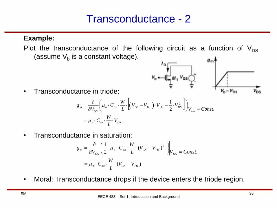
Example:
Plot the transconductance of the following circuit as a function of VDS
(assume Vb is a constant voltage).
• Moral: Transconductance drops if the device enters the triode region.
36 SM EECE 488 – Set 1: Introduction and Background
Transconductance - 3
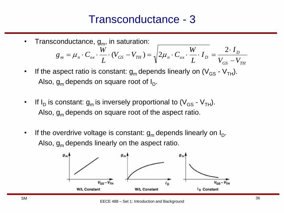
• Transconductance, gm, in saturation:
THGS
DDoxnTHGSoxnm
VV
II
L
WCVV
L
WCg
22)(
• If the aspect ratio is constant: gm depends linearly on (VGS - VTH).
Also, gm depends on square root of ID.
• If ID is constant: gm is inversely proportional to (VGS - VTH).
Also, gm depends on square root of the aspect ratio.
• If the overdrive voltage is constant: gm depends linearly on ID.
Also, gm depends linearly on the aspect ratio.
37 SM EECE 488 – Set 1: Introduction and Background
Second-Order Effects (Body Effect)
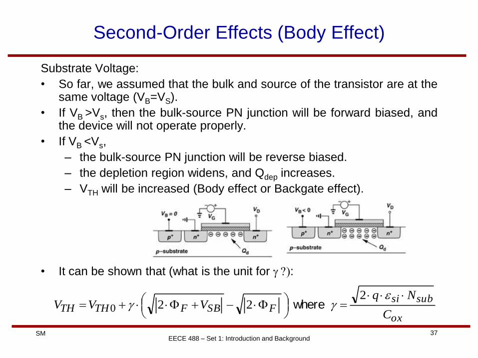
Substrate Voltage:
• So far, we assumed that the bulk and source of the transistor are at the same voltage (VB=VS).
• If VB >Vs, then the bulk-source PN junction will be forward biased, and the device will not operate properly.
• If VB <Vs,
– the bulk-source PN junction will be reverse biased.
– the depletion region widens, and Qdep increases.
– VTH will be increased (Body effect or Backgate effect).
• It can be shown that (what is the unit for g ?:
ox
subsiFSBFTHTH
C
NqVVV
gg2
220 where
38 SM EECE 488 – Set 1: Introduction and Background
Body Effect - 2
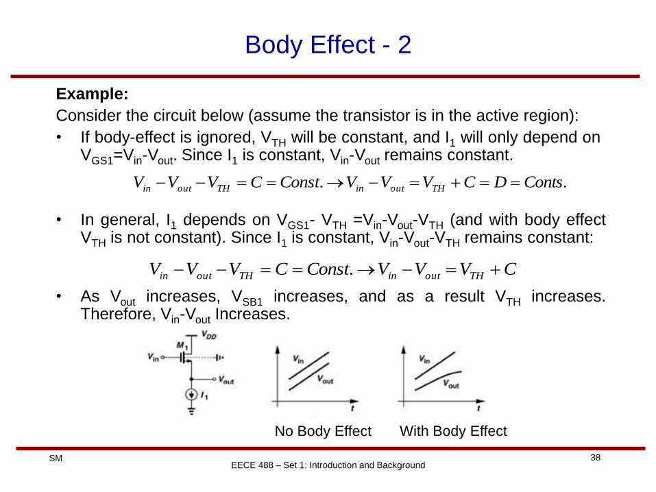
No Body Effect With Body Effect
Example:
Consider the circuit below (assume the transistor is in the active region):
• If body-effect is ignored, VTH will be constant, and I1 will only depend on VGS1=Vin-Vout. Since I1 is constant, Vin-Vout remains constant.
CVVVConstCVVV THoutinTHoutin .
• As Vout increases, VSB1 increases, and as a result VTH increases. Therefore, Vin-Vout Increases.
• In general, I1 depends on VGS1- VTH =Vin-Vout-VTH (and with body effect VTH is not constant). Since I1 is constant, Vin-Vout-VTH remains constant:
.. ContsDCVVVConstCVVV THoutinTHoutin
39 SM EECE 488 – Set 1: Introduction and Background
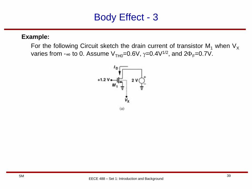
Body Effect - 3
Example:
For the following Circuit sketch the drain current of transistor M1 when VX
varies from -∞ to 0. Assume VTH0=0.6V, g=0.4V1/2, and 2F=0.7V.
40 SM EECE 488 – Set 1: Introduction and Background
Channel Length Modulation - 1
L
L
LL
LLLLLL
11
1
111
'
1
• When a transistor is in the saturation region (VDS > VGS – VTH),
the channel is pinched off.
• The drain current is LL-L'VVL
WCI THGSoxnD where2)(
'2
1
• Assuming we get: DSV
LL DSV
LLL
LL 1
11
1
'
1
• The drain current is DSTHGSoxnTHGSoxnD VVVL
WCVV
L
WCI 1
2
1 )(
'2
1 22
• As ID actually depends on both VGS and VDS, MOS transistors are
not ideal current sources (why?).
41 SM EECE 488 – Set 1: Introduction and Background
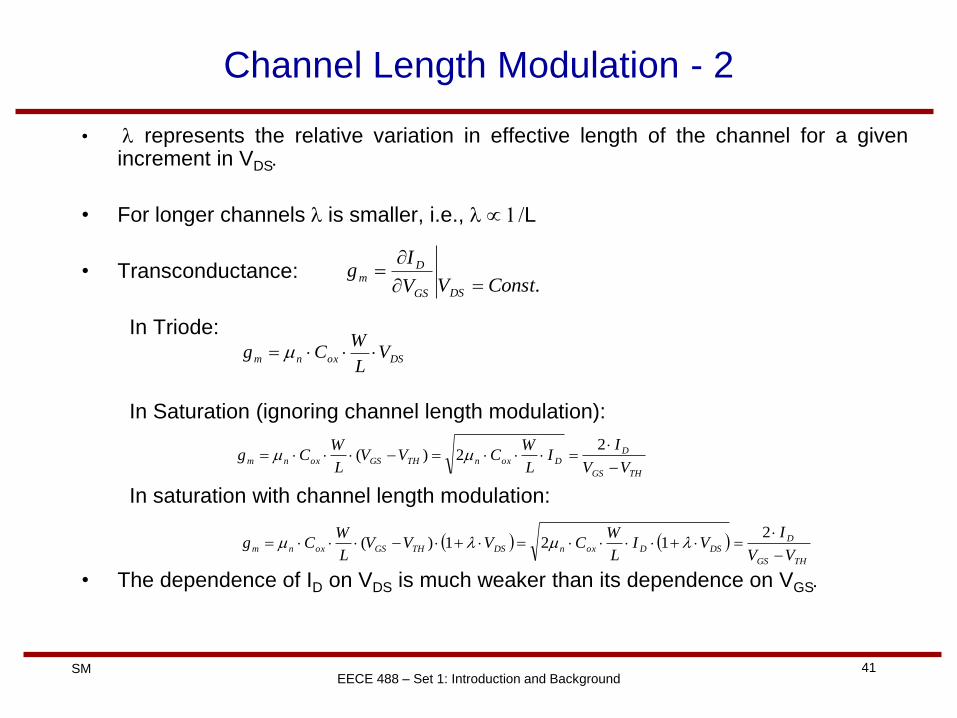
Channel Length Modulation - 2
• represents the relative variation in effective length of the channel for a given increment in VDS.
• For longer channels is smaller, i.e., 1/L
• Transconductance:
In Triode:
In Saturation (ignoring channel length modulation):
In saturation with channel length modulation:
• The dependence of ID on VDS is much weaker than its dependence on VGS.
.ConstVV
Ig
DSGS
Dm
DSoxnm VL
WCg
THGS
DDoxnTHGSoxnm
VV
II
L
WCVV
L
WCg
22)(
THGS
DDSDoxnDSTHGSoxnm
VV
IVI
L
WCVVV
L
WCg
2121)(
42 SM EECE 488 – Set 1: Introduction and Background
Channel Length Modulation - 3
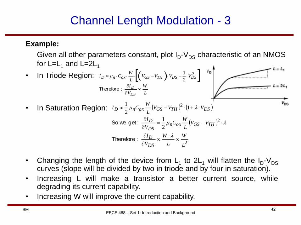
Example:
Given all other parameters constant, plot ID-VDS characteristic of an NMOS
for L=L1 and L=2L1
2
2
2
2
1
12
1
L
W
L
W
V
I
VVL
WC
V
I
VVVL
WCI
DS
D
THGSoxnDS
D
DSTHGSoxnD
:Therefore
: get weSo
• Changing the length of the device from L1 to 2L1 will flatten the ID-VDS curves (slope will be divided by two in triode and by four in saturation).
• Increasing L will make a transistor a better current source, while degrading its current capability.
• Increasing W will improve the current capability.
• In Triode Region:
• In Saturation Region:
L
W
V
I
VVVVL
WCI
DS
D
DSDSTHGSoxnD
:Therefore
2
2
1
43 SM EECE 488 – Set 1: Introduction and Background
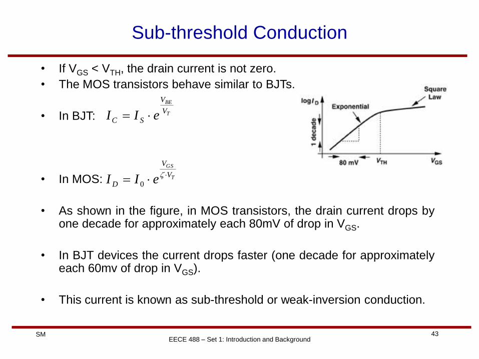
Sub-threshold Conduction
• If VGS < VTH, the drain current is not zero.
• The MOS transistors behave similar to BJTs.
• In BJT:
• In MOS:
• As shown in the figure, in MOS transistors, the drain current drops by one decade for approximately each 80mV of drop in VGS.
• In BJT devices the current drops faster (one decade for approximately each 60mv of drop in VGS).
• This current is known as sub-threshold or weak-inversion conduction.
T
BE
V
V
SC eII
T
GS
V
V
D eII
0
44 SM EECE 488 – Set 1: Introduction and Background
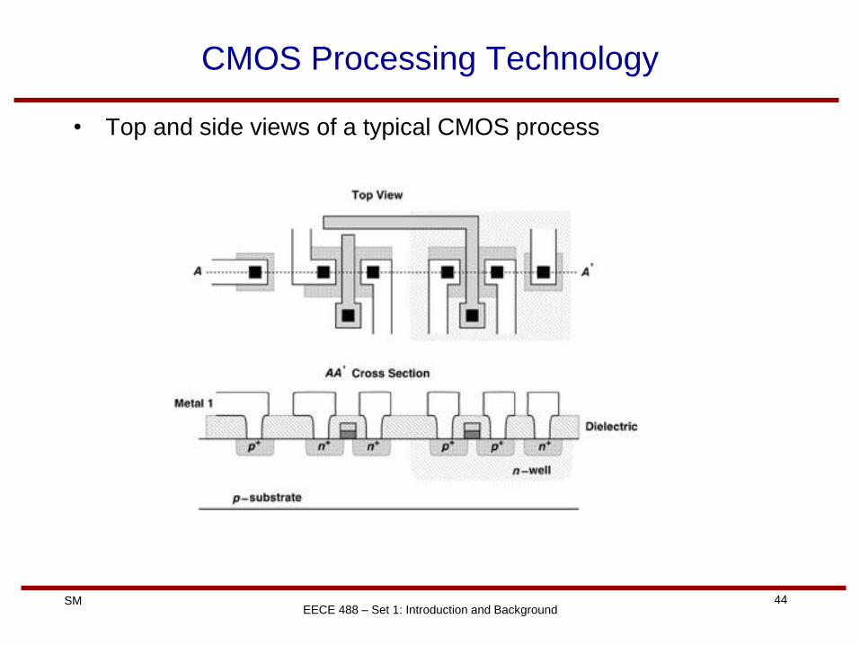
CMOS Processing Technology
• Top and side views of a typical CMOS process
45 SM EECE 488 – Set 1: Introduction and Background
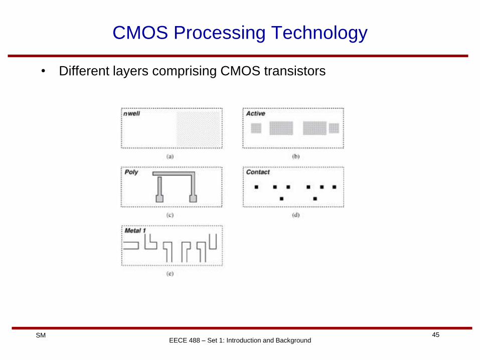
CMOS Processing Technology
• Different layers comprising CMOS transistors
46 SM EECE 488 – Set 1: Introduction and Background
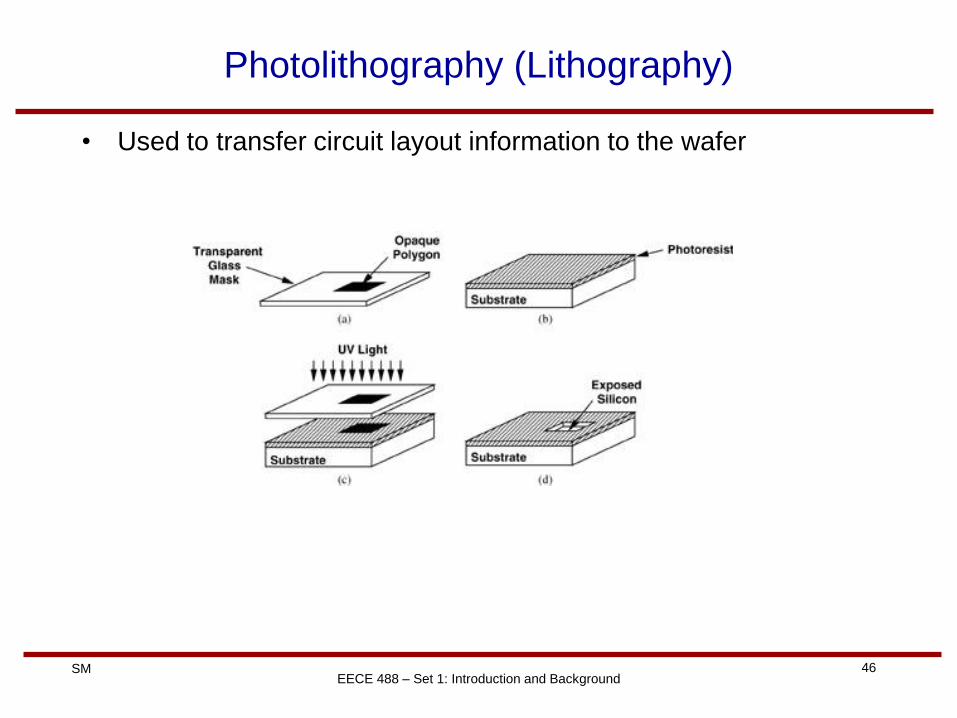
Photolithography (Lithography)
• Used to transfer circuit layout information to the wafer
47 SM
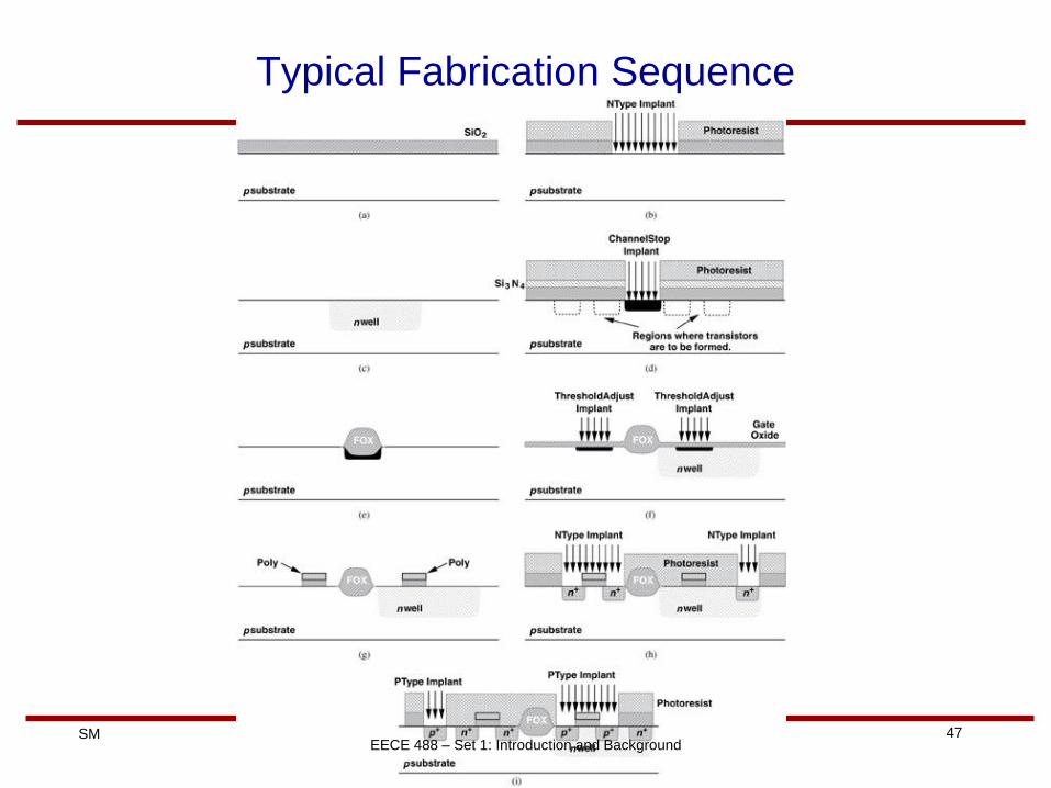
Typical Fabrication Sequence
EECE 488 – Set 1: Introduction and Background
48 SM EECE 488 – Set 1: Introduction and Background
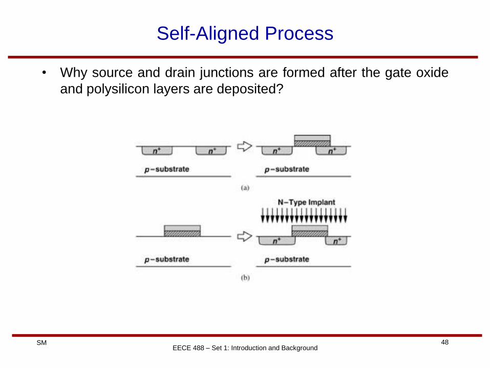
Self-Aligned Process
• Why source and drain junctions are formed after the gate oxide
and polysilicon layers are deposited?
49 SM EECE 488 – Set 1: Introduction and Background
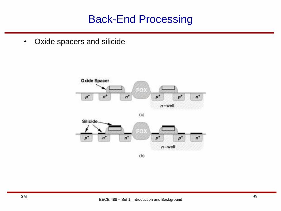
Back-End Processing
• Oxide spacers and silicide
50 SM EECE 488 – Set 1: Introduction and Background
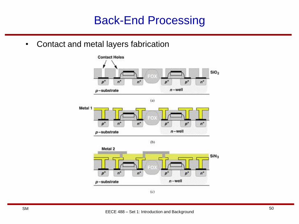
Back-End Processing
• Contact and metal layers fabrication
51 SM EECE 488 – Set 1: Introduction and Background
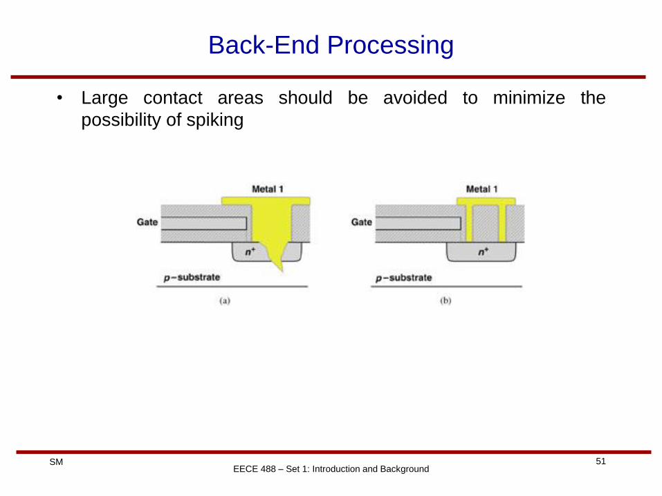
Back-End Processing
• Large contact areas should be avoided to minimize the
possibility of spiking
52 SM EECE 488 – Set 1: Introduction and Background
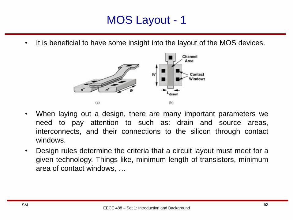
MOS Layout - 1
• It is beneficial to have some insight into the layout of the MOS devices.
• When laying out a design, there are many important parameters we
need to pay attention to such as: drain and source areas,
interconnects, and their connections to the silicon through contact
windows.
• Design rules determine the criteria that a circuit layout must meet for a
given technology. Things like, minimum length of transistors, minimum
area of contact windows, …
53 SM EECE 488 – Set 1: Introduction and Background
MOS Layout - 2
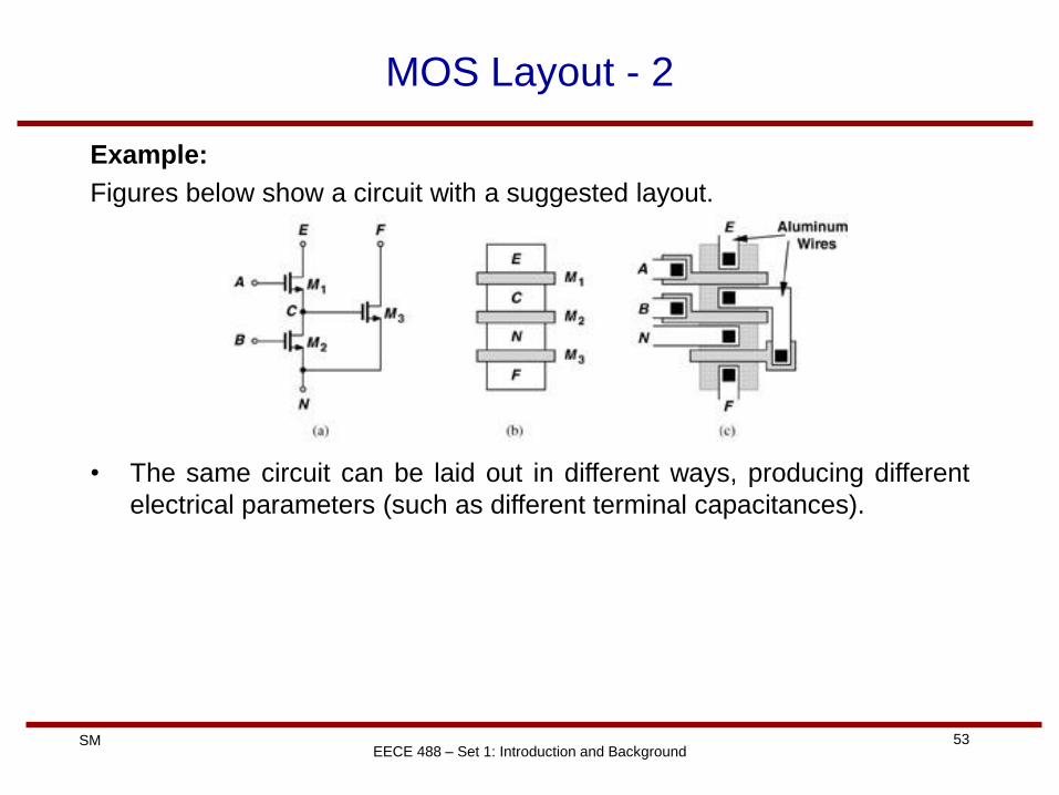
Example:
Figures below show a circuit with a suggested layout.
• The same circuit can be laid out in different ways, producing different
electrical parameters (such as different terminal capacitances).
54 SM EECE 488 – Set 1: Introduction and Background
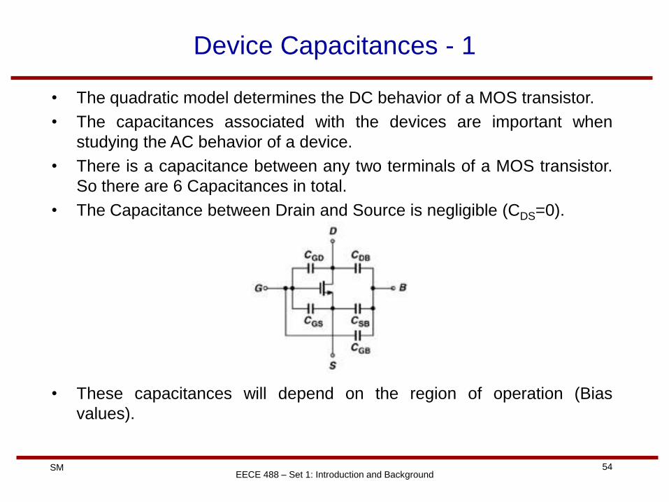
Device Capacitances - 1
• The quadratic model determines the DC behavior of a MOS transistor.
• The capacitances associated with the devices are important when
studying the AC behavior of a device.
• There is a capacitance between any two terminals of a MOS transistor.
So there are 6 Capacitances in total.
• The Capacitance between Drain and Source is negligible (CDS=0).
• These capacitances will depend on the region of operation (Bias
values).
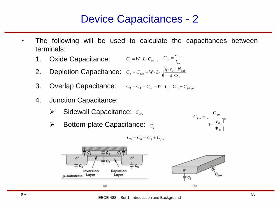
55 SM EECE 488 – Set 1: Introduction and Background
Device Capacitances - 2
• The following will be used to calculate the capacitances between
terminals:
1. Oxide Capacitance: ,
2. Depletion Capacitance:
3. Overlap Capacitance:
4. Junction Capacitance:
Sidewall Capacitance:
Bottom-plate Capacitance:
oxCLWC 1ox
oxox
tC
F
subsi
dep
NqLWCC
42
fringeoxDov CCLWCCC 43
m
B
R
j
jun
V
CC
1
0jswC
jC
jswj CCCC 65
56 SM EECE 488 – Set 1: Introduction and Background
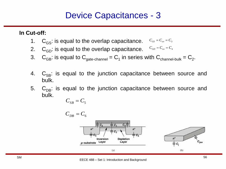
Device Capacitances - 3
In Cut-off:
1. CGS: is equal to the overlap capacitance.
2. CGD: is equal to the overlap capacitance.
3. CGB: is equal to Cgate-channel = C1 in series with Cchannel-bulk = C2.
4. CSB: is equal to the junction capacitance between source and
bulk.
5. CDB: is equal to the junction capacitance between source and
bulk.
3CCC ovGS
4CCC ovGD
5CCSB
6CCDB
57 SM EECE 488 – Set 1: Introduction and Background
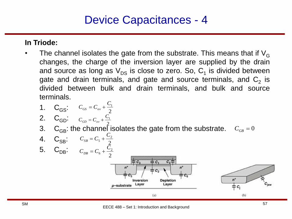
Device Capacitances - 4
In Triode:
• The channel isolates the gate from the substrate. This means that if VG
changes, the charge of the inversion layer are supplied by the drain
and source as long as VDS is close to zero. So, C1 is divided between
gate and drain terminals, and gate and source terminals, and C2 is
divided between bulk and drain terminals, and bulk and source
terminals.
1. CGS:
2. CGD:
3. CGB: the channel isolates the gate from the substrate.
4. CSB:
5. CDB:
0GBC
2
1CCC ovGS
2
25
CCCSB
2
26
CCCDB
2
1CCC ovGD
58 SM EECE 488 – Set 1: Introduction and Background
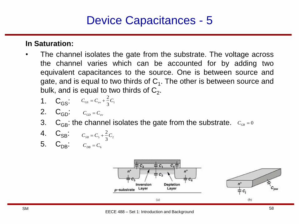
Device Capacitances - 5
In Saturation:
• The channel isolates the gate from the substrate. The voltage across
the channel varies which can be accounted for by adding two
equivalent capacitances to the source. One is between source and
gate, and is equal to two thirds of C1. The other is between source and
bulk, and is equal to two thirds of C2.
1. CGS:
2. CGD:
3. CGB: the channel isolates the gate from the substrate.
4. CSB:
5. CDB:
0GBC
13
2CCC ovGS
253
2CCCSB
6CCDB
ovGD CC
59 SM EECE 488 – Set 1: Introduction and Background
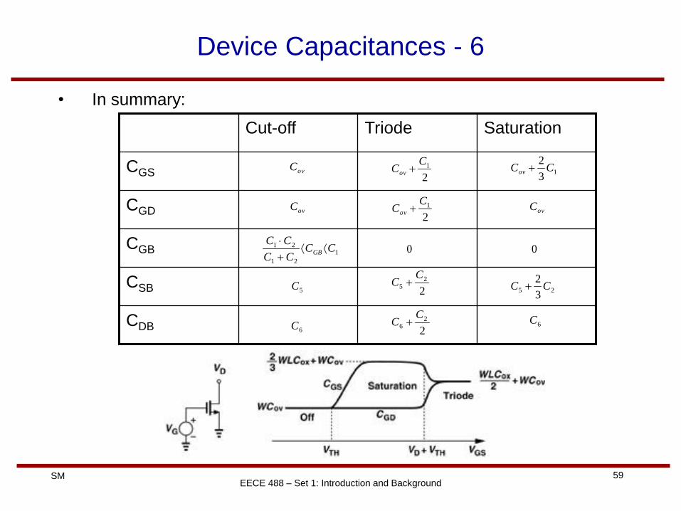
Device Capacitances - 6
• In summary:
CDB
CSB
CGB
CGD
CGS
Saturation Triode Cut-off
ovC
ovC ovC
13
2CCov
253
2CC
0
6C2
26
CC
2
25
CC
2
1CCov
2
1CCov
01
21
21 CCCC
CCGB
6C
5C
60 SM EECE 488 – Set 1: Introduction and Background
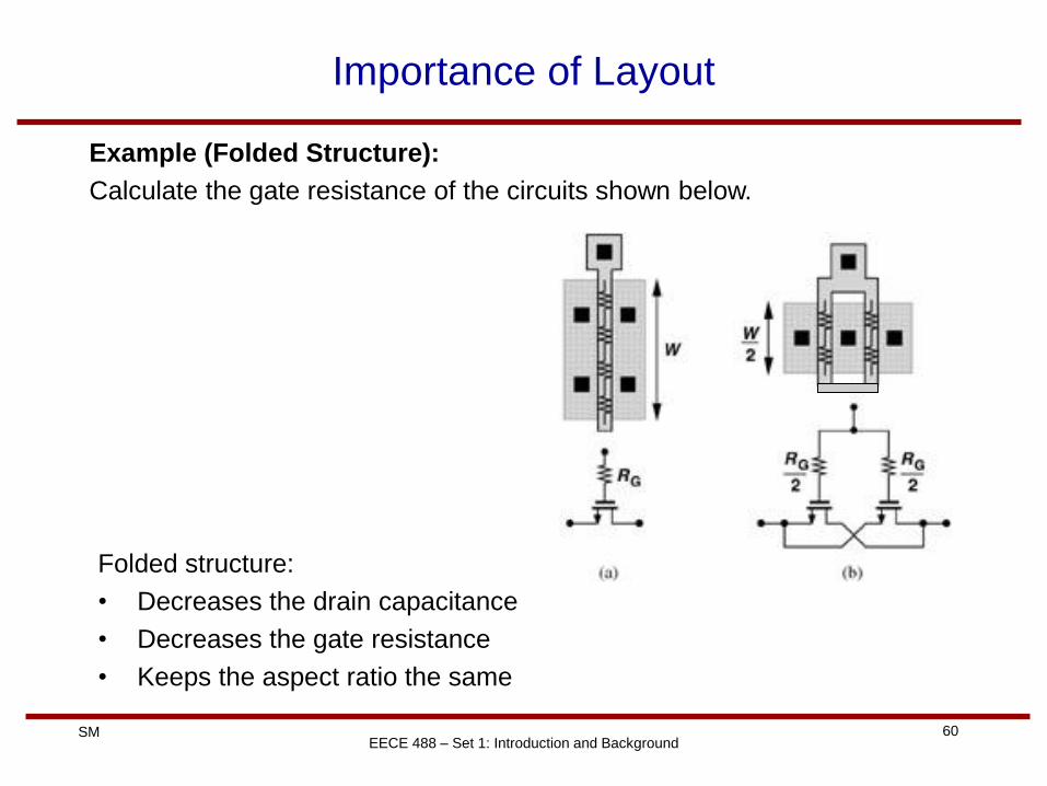
Importance of Layout
Example (Folded Structure):
Calculate the gate resistance of the circuits shown below.
Folded structure:
• Decreases the drain capacitance
• Decreases the gate resistance
• Keeps the aspect ratio the same
61 SM EECE 488 – Set 1: Introduction and Background
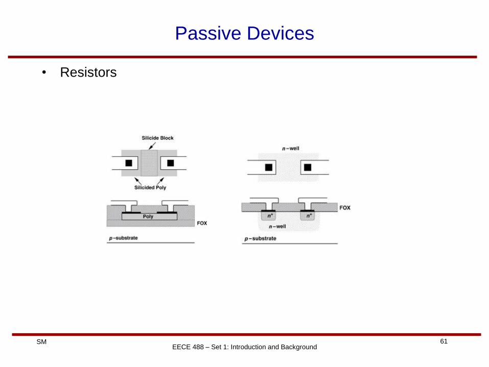
Passive Devices
• Resistors
62 SM EECE 488 – Set 1: Introduction and Background
Passive Devices
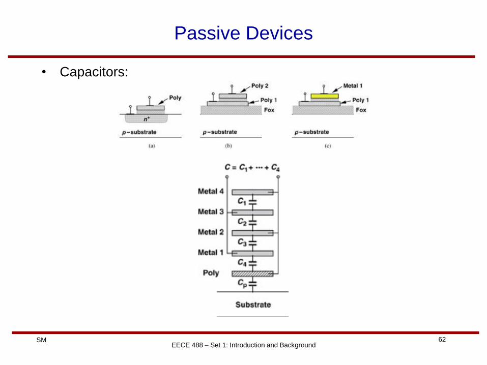
• Capacitors:
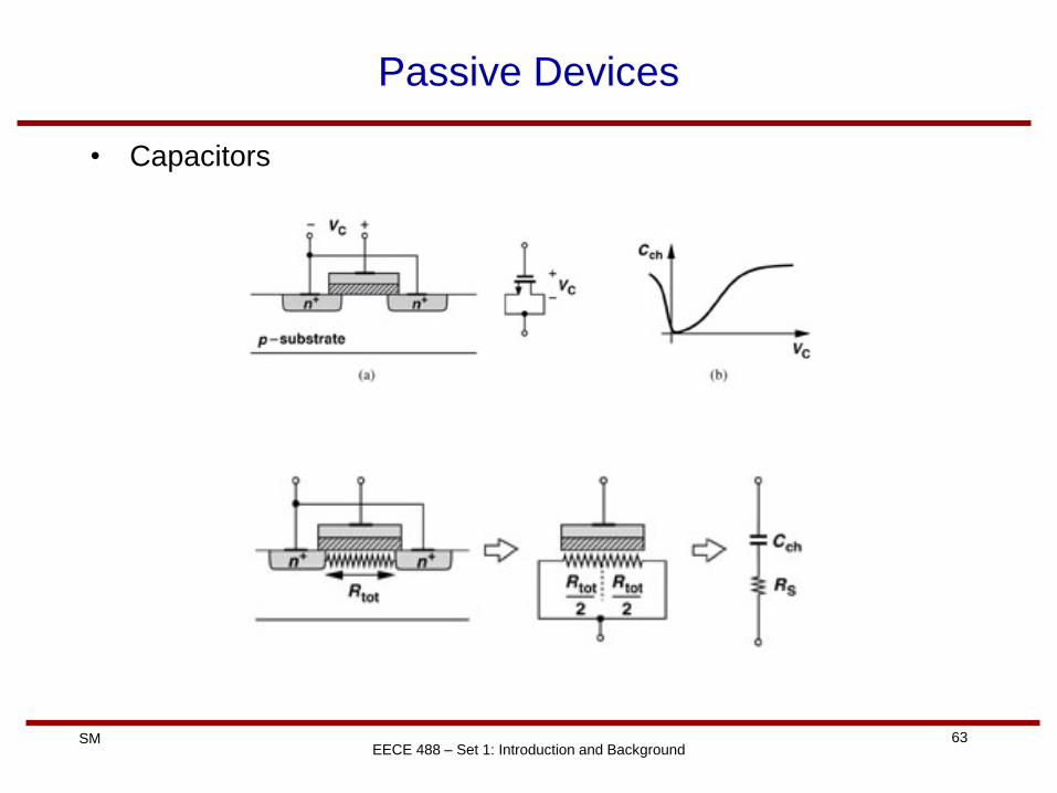
63 SM EECE 488 – Set 1: Introduction and Background
Passive Devices
• Capacitors
64 SM EECE 488 – Set 1: Introduction and Background
Passive Devices
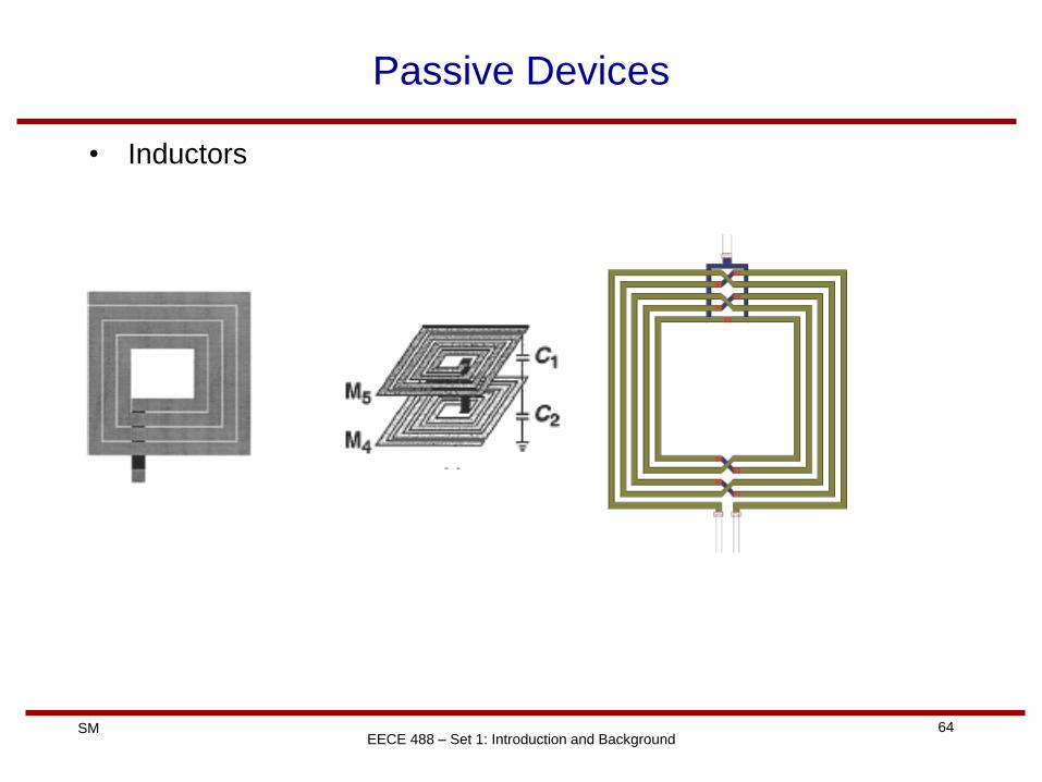
• Inductors
65 SM EECE 488 – Set 1: Introduction and Background
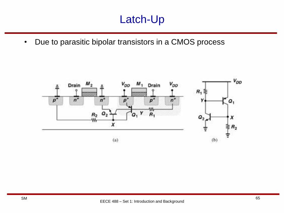
Latch-Up
• Due to parasitic bipolar transistors in a CMOS process
66 SM EECE 488 – Set 1: Introduction and Background
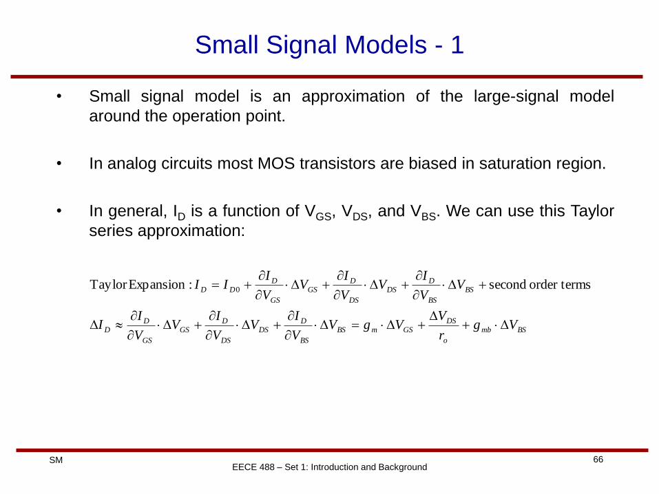
Small Signal Models - 1
• Small signal model is an approximation of the large-signal model
around the operation point.
• In analog circuits most MOS transistors are biased in saturation region.
• In general, ID is a function of VGS, VDS, and VBS. We can use this Taylor
series approximation:
BSmb
o
DSGSmBS
BS
DDS
DS
DGS
GS
DD
BS
BS
DDS
DS
DGS
GS
DDD
Vgr
VVgV
V
IV
V
IV
V
II
VV
IV
V
IV
V
III
sorder term second :ExpansionTaylor 0
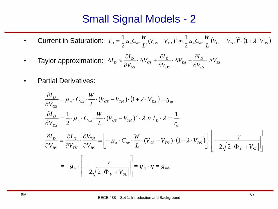
67 SM EECE 488 – Set 1: Introduction and Background
Small Signal Models - 2
• Current in Saturation:
• Taylor approximation:
• Partial Derivatives:
DSTHGSoxnTHGSoxnD VVVL
WCVV
L
WCI 1
2
1 )(
'2
1 22
BS
BS
DDS
DS
DGS
GS
DD V
V
IV
V
IV
V
II
mbm
SBF
m
SBF
DSTHGSoxn
BS
TH
TH
D
BS
D
o
DTHGSoxn
DS
D
mDSTHGSoxn
GS
D
ggV
g
VVVV
L
WC
V
V
V
I
V
I
rIVV
L
WC
V
I
gVVVL
WC
V
I
g
g
22
221)(
1)(
2
1
1)(
2
68 SM EECE 488 – Set 1: Introduction and Background
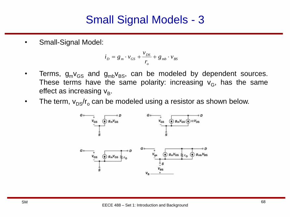
Small Signal Models - 3
• Small-Signal Model:
BSmb
o
DSGSmD vg
r
vvgi
• Terms, gmvGS and gmbvBS, can be modeled by dependent sources.
These terms have the same polarity: increasing vG, has the same
effect as increasing vB.
• The term, vDS/ro can be modeled using a resistor as shown below.
69 SM EECE 488 – Set 1: Introduction and Background
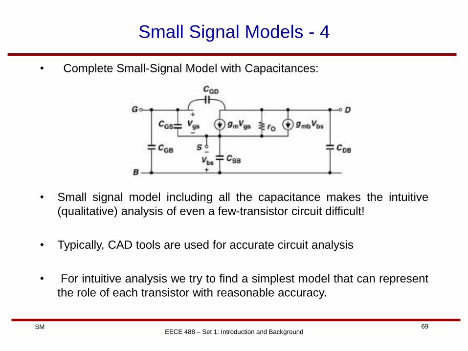
Small Signal Models - 4
• Complete Small-Signal Model with Capacitances:
• Small signal model including all the capacitance makes the intuitive
(qualitative) analysis of even a few-transistor circuit difficult!
• Typically, CAD tools are used for accurate circuit analysis
• For intuitive analysis we try to find a simplest model that can represent
the role of each transistor with reasonable accuracy.
70 SM EECE 488 – Set 1: Introduction and Background
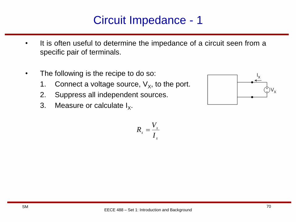
Circuit Impedance - 1
• It is often useful to determine the impedance of a circuit seen from a
specific pair of terminals.
• The following is the recipe to do so:
1. Connect a voltage source, VX, to the port.
2. Suppress all independent sources.
3. Measure or calculate IX.
X
X
X
I
VR
71 SM EECE 488 – Set 1: Introduction and Background
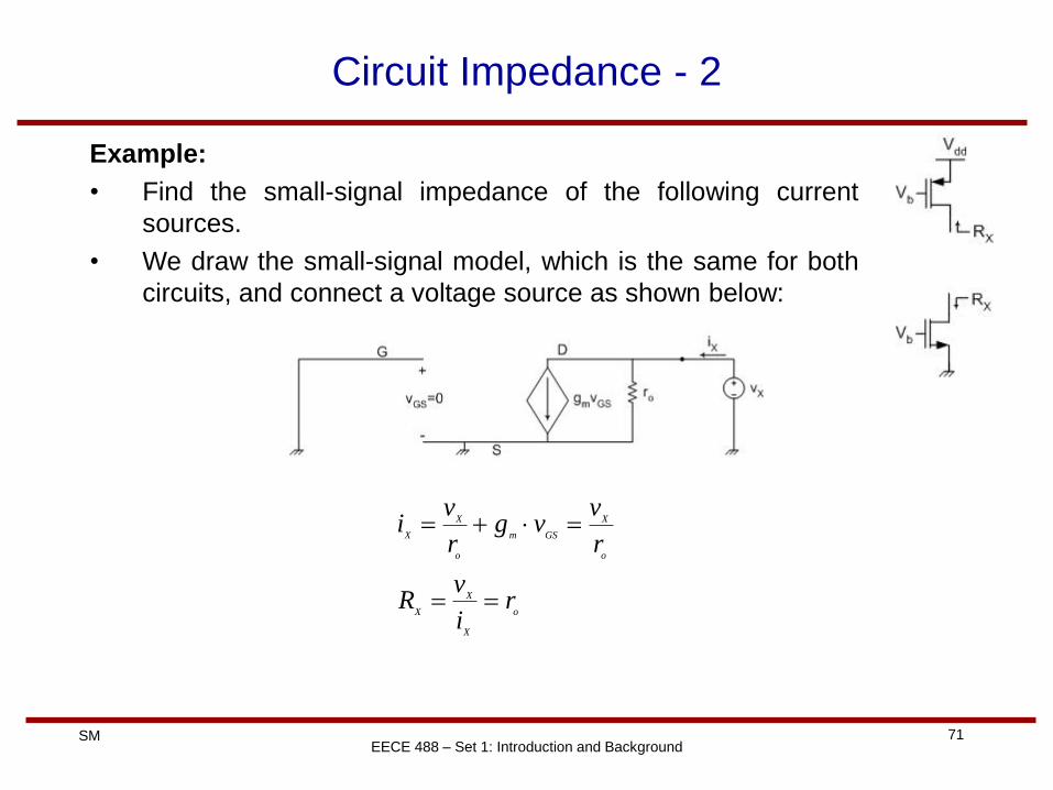
Circuit Impedance - 2
Example:
• Find the small-signal impedance of the following current
sources.
• We draw the small-signal model, which is the same for both
circuits, and connect a voltage source as shown below:
o
X
X
X
o
X
GSm
o
X
X
ri
vR
r
vvg
r
vi
72 SM EECE 488 – Set 1: Introduction and Background
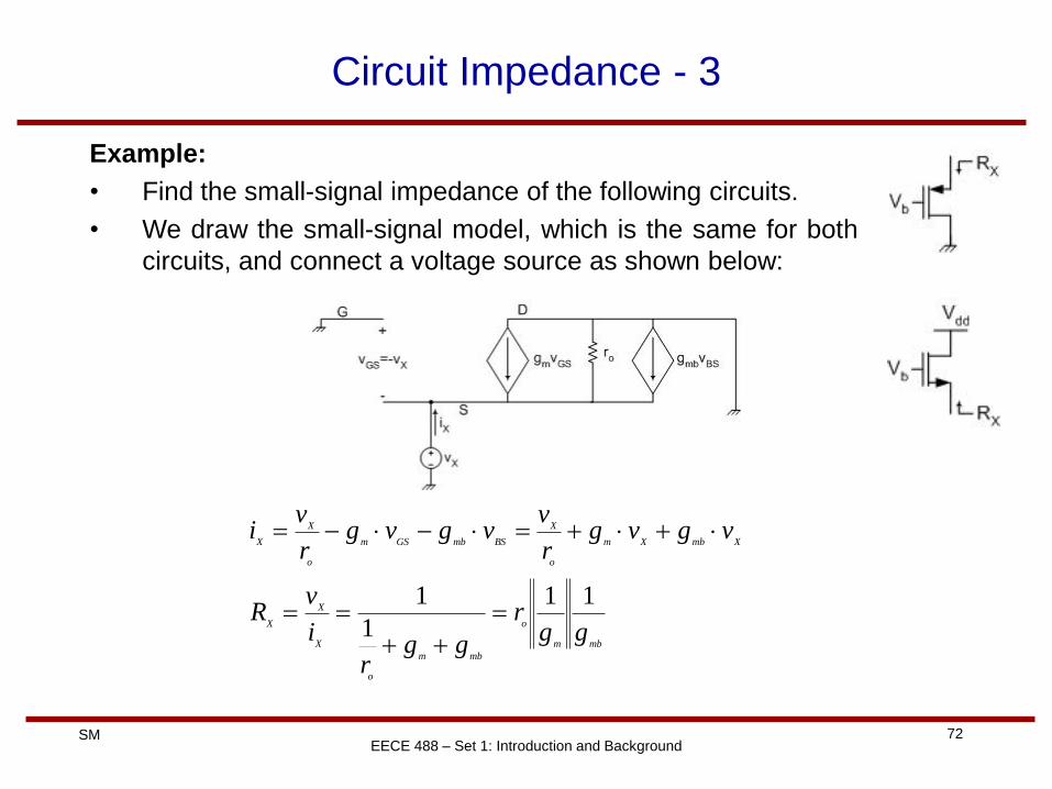
Circuit Impedance - 3
Example:
• Find the small-signal impedance of the following circuits.
• We draw the small-signal model, which is the same for both
circuits, and connect a voltage source as shown below:
mbm
o
mbm
o
X
X
X
XmbXm
o
X
BSmbGSm
o
X
X
ggr
ggr
i
vR
vgvgr
vvgvg
r
vi
11
1
1
73 SM EECE 488 – Set 1: Introduction and Background
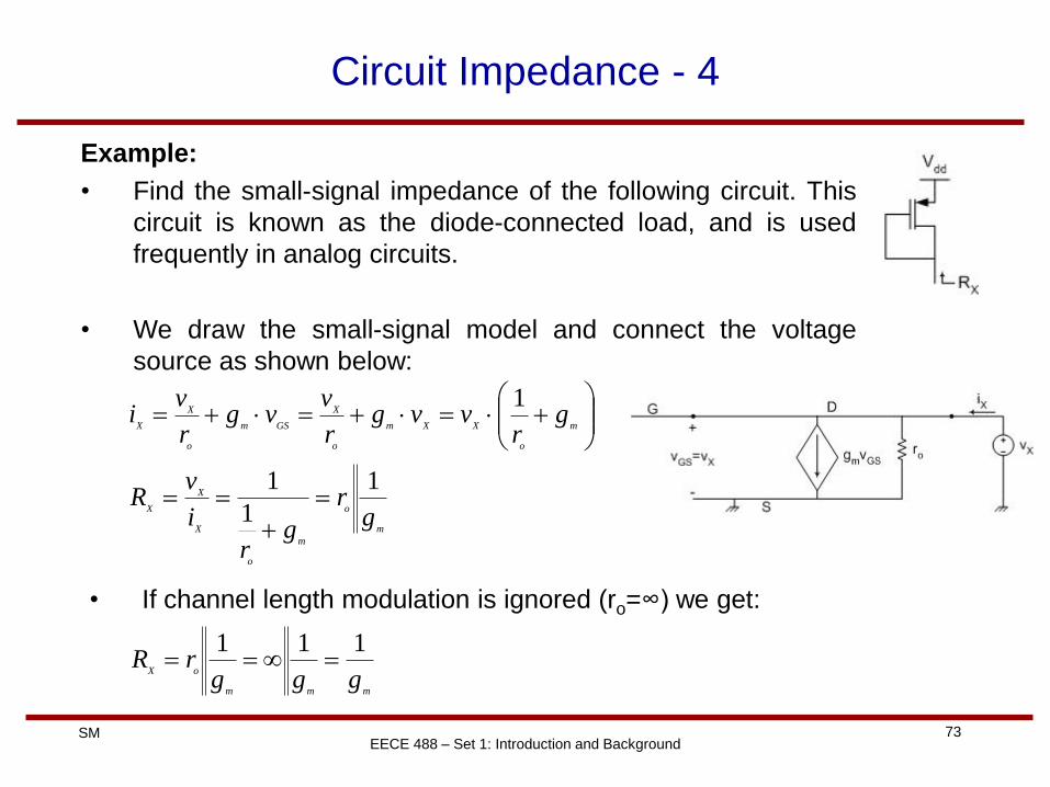
Circuit Impedance - 4
Example:
• Find the small-signal impedance of the following circuit. This
circuit is known as the diode-connected load, and is used
frequently in analog circuits.
• We draw the small-signal model and connect the voltage
source as shown below:
m
o
m
o
X
X
X
m
o
XXm
o
X
GSm
o
X
X
gr
gr
i
vR
gr
vvgr
vvg
r
vi
1
1
1
1
• If channel length modulation is ignored (ro=∞) we get:
mmm
oX
gggrR
111
74 SM EECE 488 – Set 1: Introduction and Background
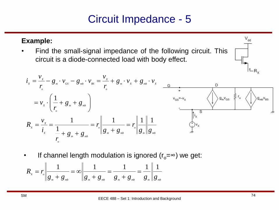
Circuit Impedance - 5
Example:
• Find the small-signal impedance of the following circuit. This
circuit is a diode-connected load with body effect.
mbm
o
mbm
o
mbm
o
X
X
X
mbm
o
X
XmbXm
o
X
BSmbGSm
o
X
X
ggr
ggr
ggr
i
vR
ggr
v
vgvgr
vvgvg
r
vi
111
1
1
1
• If channel length modulation is ignored (ro=∞) we get:
mbmmbmmbmmbm
oX
ggggggggrR
11111
75 SM EECE 488 – Set 1: Introduction and Background
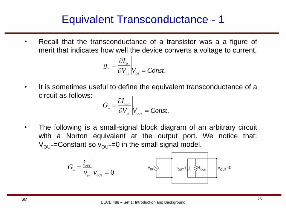
Equivalent Transconductance - 1
• Recall that the transconductance of a transistor was a a figure of
merit that indicates how well the device converts a voltage to current.
• It is sometimes useful to define the equivalent transconductance of a
circuit as follows:
.ConstVV
Ig
DSGS
D
m
.ConstVV
IG
OUTIN
OUT
m
• The following is a small-signal block diagram of an arbitrary circuit
with a Norton equivalent at the output port. We notice that:
VOUT=Constant so vOUT=0 in the small signal model.
0
OUTIN
OUT
m
vv
iG
76 SM EECE 488 – Set 1: Introduction and Background
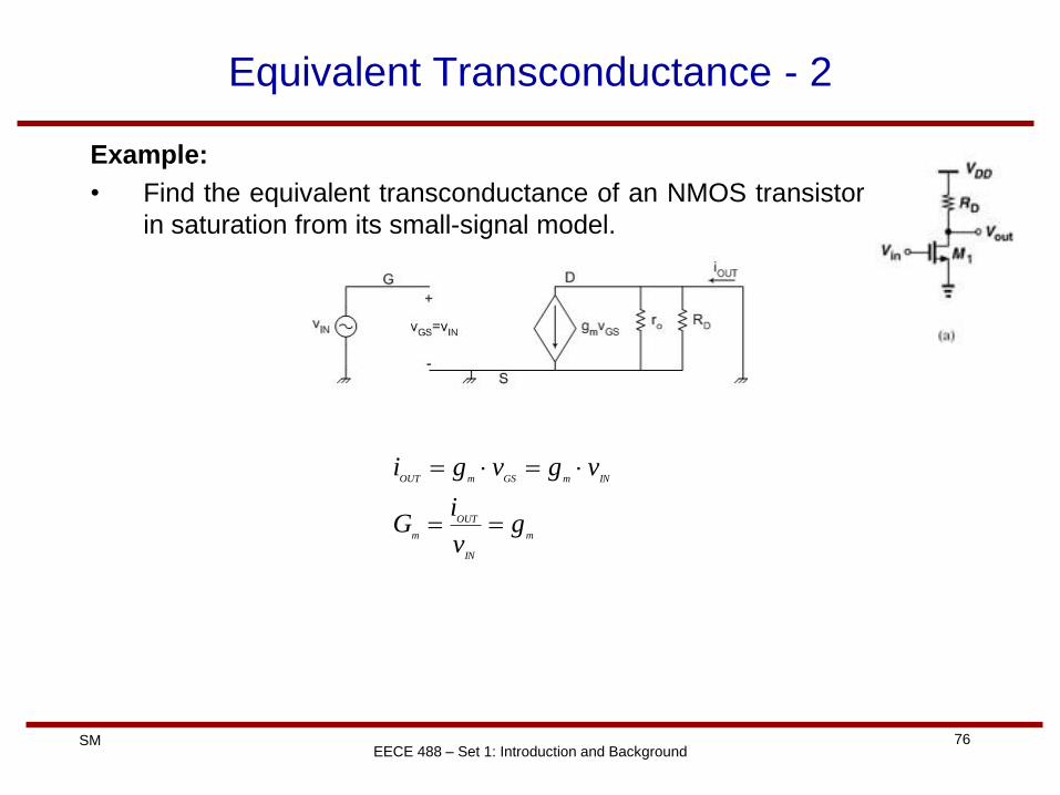
Equivalent Transconductance - 2
Example:
• Find the equivalent transconductance of an NMOS transistor
in saturation from its small-signal model.
m
IN
OUT
m
INmGSmOUT
gv
iG
vgvgi
77 SM EECE 488 – Set 1: Introduction and Background
Equivalent Transconductance - 3
Example:
• Find the equivalent transconductance of the following circuit
when the NMOS transistor in saturation.
SSmbSmOO
Om
O
S
SmbSm
m
IN
OUT
m
INm
O
S
SmbSmOUT
O
SOUT
SOUTmbSOUTINm
O
S
BSmbGSmOUT
SOUTGSSGSIN
RRgRgrr
rg
r
RRgRg
g
v
iG
vgr
RRgRgi
r
RiRigRivg
r
vvgvgi
Rivvvv
1
1
)(
78 SM EECE 488 – Set 1: Introduction and Background
Short-Channel Effects
• Threshold Reduction
– Drain-induced barrier lowering (DIBL)
• Mobility degradation
• Velocity saturation
• Hot carrier effects
– Substrate current
– Gate current
• Output impedance variation
79 SM EECE 488 – Set 1: Introduction and Background
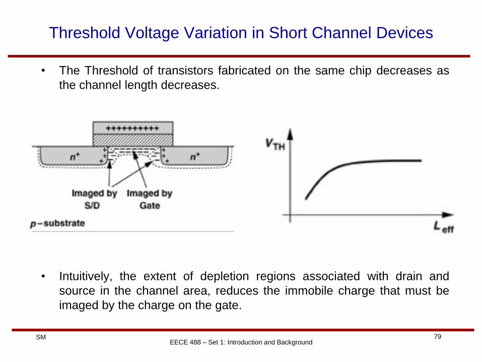
Threshold Voltage Variation in Short Channel Devices
• The Threshold of transistors fabricated on the same chip decreases as
the channel length decreases.
• Intuitively, the extent of depletion regions associated with drain and
source in the channel area, reduces the immobile charge that must be
imaged by the charge on the gate.
80 SM EECE 488 – Set 1: Introduction and Background
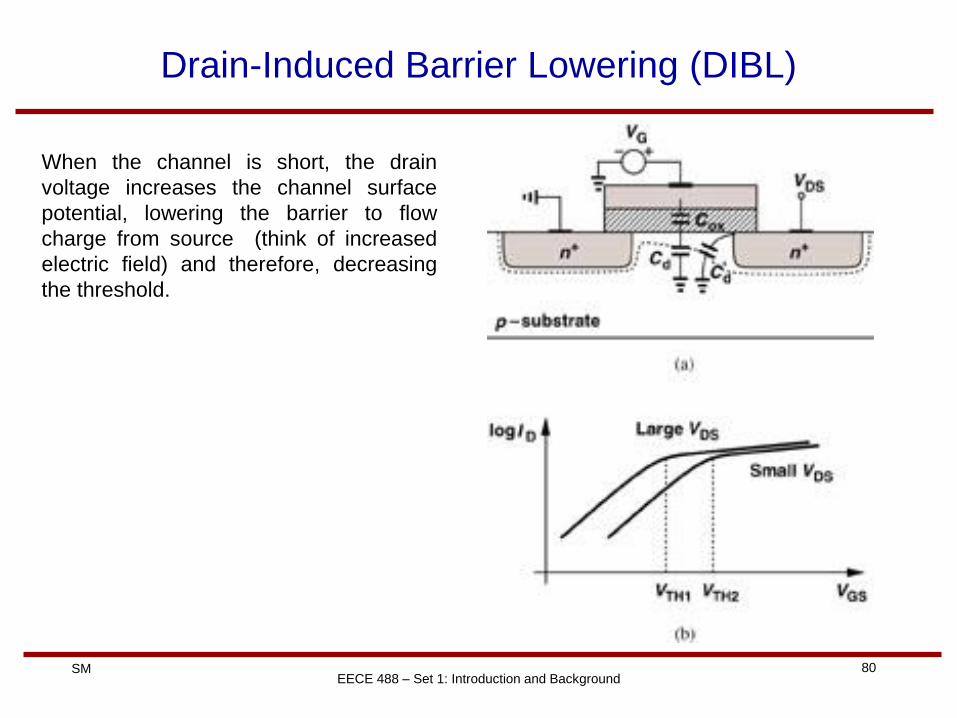
Drain-Induced Barrier Lowering (DIBL)
When the channel is short, the drain
voltage increases the channel surface
potential, lowering the barrier to flow
charge from source (think of increased
electric field) and therefore, decreasing
the threshold.
81 SM EECE 488 – Set 1: Introduction and Background
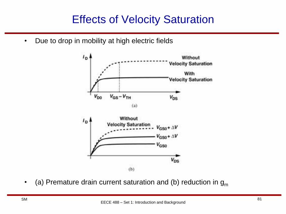
Effects of Velocity Saturation
• Due to drop in mobility at high electric fields
• (a) Premature drain current saturation and (b) reduction in gm
82 SM EECE 488 – Set 1: Introduction and Background
Hot Carrier Effects
• Short channel devices may experience high lateral drain-source
electric field
• Some carriers that make it to drain have high velocity (called
“hot” carriers)
• “Hot” carriers may “hit” silicon atoms at high speed and cause
impact ionization
• The resulting electron and holes are absorbed by the drain and
substrate causing extra drain-substrate current
• Really “hot” carriers may be injected into gate oxide and flow out
of gate causing gate current!
83 SM EECE 488 – Set 1: Introduction and Background
Output Impedance Variation
Recall the definition of .
84 SM EECE 488 – Set 1: Introduction and Background
Output Impedance Variation in Short-Channel Devices