Embed Size (px)
DESCRIPTION
EEM 486 : Computer Architecture Lecture 4 Designing a Multicycle Processor. Processor. Input. Control. Memory. Datapath. Output. The Big Picture. Designing a Multiple Clock Cycle Datapath. OPcode. Control Logic / Store (PLA, ROM). Decode. microinstruction. Conditions. - PowerPoint PPT Presentation
Citation preview

EEM 486
EEM 486: Computer Architecture
Lecture 4
Designing a Multicycle Processor

Lec 4.2
The Big Picture
Designing a Multiple Clock Cycle Datapath
Control
Datapath
Memory
Processor
Input
Output

Lec 4.3
Single-Cycle Processor
In our single-cycle processor, each instruction is realized
by exactly one control command or microinstruction
Control Logic / Store (PLA, ROM)
OPcode
Datapath
Inst
ruct
ion
Decode
Condit
ions
ControlPoints
microinstruction

Lec 4.4
Abstract View of Single Cycle-Processor
PC
Next
PC
Regis
ter
Fetc
h ALU
Reg.
Wrt
Mem
Acc
ess
Data
MemInst
ruct
ion
Fetc
h
ALU
ctr
RegD
st
ALU
Src
ExtO
p
Mem
Wr
Equal
nPC
_sel
RegW
r
Mem
Wr
Mem
Rd
MainControl
ALUcontrol
op
fun
Ext

Lec 4.5
What’s Wrong with CPI=1 Processor?
Long Cycle Time
All instructions take as much time as the slowest
Real memory is not as nice as our idealized memory• Cannot always get the job done in one (short) cycle
PC Inst Memory mux ALU Data Mem mux
PC Reg FileInst Memory mux ALU mux
PC Inst Memory mux ALU Data Mem
PC Inst Memory cmp mux
Reg File
Reg File
Reg File
Arithmetic & Logical
Load
Store
Branch
Critical Path
setup
setup

Lec 4.6
Memory Access Time Physics => fast memories are small (large memories are
slow)
=> Use a hierarchy of memories
Storage Arrayselected word line
addressstorage cellbit line
sense ampsaddressdecoder
CacheProcessor
1 time-period
pro
c. b
us
L2Cache
mem
. bus
2-3 time-periods20 - 50 time-periods
memory

Lec 4.7
Break up the instructions into steps:• Let each step take one “smaller” clock cycle
- Balance the amount of work to be done
- Restrict each cycle to use only one major functional unit
Major functional units: Memory, Register File, and ALU
• Let different instructions take different numbers of cycles
Use a functional unit more than once within execution of one instruction (Less hardware)• A single memory unit for both instructions and data
• A single ALU, rather than an ALU and two adders
At the end of a cycle• store values for use in later cycles
• introduce additional “internal” registers
Multicycle Approach

Lec 4.8
Partitioning the CPI=1 Datapath Add registers between smallest steps
PC
Next
PC
Opera
nd
Fetc
h Exec Reg.
File
Mem
Acc
ess
Data
Mem
Inst
ruct
ion
Fetc
h
ALU
ctr
RegD
st
ALU
Src
ExtO
p
Mem
Wr
nPC
_sel
RegW
r
Mem
Wr
Mem
Rd
Equ
al
Instruction fetch
Decode and Operand fetch
Execution Memory access
Writeback
Lec 4.9
Recall: Step-by-step Processor Design
Step 1: ISA => Logical Register Transfers
Step 2: Components of the Datapath
Step 3: RTL + Components => Datapath
Step 4: Datapath + Logical RTs => Physical RTs
Step 5: Physical RTs => Control

Lec 4.10
Step 4: R-type (add, sub, . . .)inst Logical Register Transfers
ADDU R[rd]<–R[rs] + R[rt]; PC <– PC + 4
Step 1. Instruction Fetch
IR ← MEM[PC], PC ← PC + 4
Step 2. Instruction Decode and Register Fetch
A ← R[rs], B ← R[rt]
Step 3. Execution
ALUOut ← A op B
Step 4. Write-back
R[rd] ← ALUOut

Lec 4.11
R-type - Fetch
4
ALU
Instruction register
Address
MemData
Memory
MemRead=1 IRWrite=1
ALUctr=Add
nPCWrite=1
PC
WriteData

Lec 4.12
R-type – Decode/Register Fetch
PC
A
B 4
ALU
Rs
Rw
Rt Registers
Write data
Read data 1
Read data 2
Instruction [25-21]
Instruction [20-16]
Instruction [15-11]
Instruction register
Address
MemData
Writedata
Memory
MemRead=0 IRWrite=0 RegWrite=0
ALUctr=x
nPCWrite=0

Lec 4.13
R-type - Execution
PC
A
B
0
1
0
14
ALU ALUOut
Rs
Rw
Rt Registers
Write data
Read data 1
Read data 2
Instruction [25-21]
Instruction [20-16]
Instruction [15-11]
Instruction register
Address
MemData
Writedata
Memory
MemRead=0 IRWrite=0 RegWrite=0 ALUSrcA=1
ALUSrcB=0 ALUctr= Func
nPCWrite=0

Lec 4.14
R-type – Write Back
PC
A
B
0
1
0
14
ALU ALUOut
Rs
Rw
Rt Registers
Write data
Read data 1
Read data 2
Instruction [25-21]
Instruction [20-16]
Instruction [15-11]
Instruction register
Address
MemData
Writedata
Memory
MemRead=0 IRWrite=0 RegWrite=1 ALUSrcA=x
ALUSrcB=x ALUctr=x
nPCWrite=0

Lec 4.15
Step 4: Logical immedinst Logical Register Transfers
ORI R[rt] <– R[rs] OR ZExt(Im16); PC <– PC + 4
Step 1. Instruction Fetch
IR ← MEM[PC], PC ← PC + 4
Step 2. Instruction Decode and Register Fetch
A ← R[rs]
Step 3. Execution
ALUOut ← A OR ZExt(Im16)
Step 4. Write-back
R[rt] ← ALUOut

Lec 4.16
Logical immediate - Execution
PC
Inst [15-11]
A
B
0
1
0
14
ALU ALUOut
Rs
Rw
Rt Registers
Write data
Read data 1
Read data 2
Instruction [25-21]
Instruction [20-16]
Instruction [15-0]
Instruction register
Address
MemData
Writedata
Memory
MemRead=0 IRWrite=0 RegWrite=0 ALUSrcA=1
ALUSrcB=2 ALUctr=Or
nPCWrite=0
2
Zeroextend16 32

Lec 4.17
Logical immediate – Write Back
PC
Inst [15-11]
A
B
0
1
0
14
ALU ALUOut
Rs
Rw
Rt Registers
Write data
Read data 1
Read data 2
Instruction [25-21]
Instruction [20-16]
Instruction [15-0]
Instruction register
Address
MemData
Writedata
Memory
MemRead=0 IRWrite=0 RegWrite=1 ALUSrcA=x
ALUSrcB=x ALUctr=x
nPCWrite=0
2
Zeroextend
0
1
RegDst=0
16 32

Lec 4.18
Step 4 : Loadinst Logical Register Transfers
LW R[rt] <– MEM[R[rs] + SExt(Im16)]; PC <– PC + 4
Step 1. Instruction Fetch
IR ← MEM[PC], PC ← PC + 4
Step 2. Instruction Decode and Register Fetch
A ← R[rs]
Step 3. Memory address computation
ALUOut ← A + SExt(Im16)
Step 4. Memory access
MDR ← Memory[ALUOut]
Step 5. Load completion
R[rt] ← MDR

Lec 4.19
Load: Address Calculation
PC
Inst [15-11]
A
B
0
1
0
14
ALU
ALUOut
Rs
Rw
Rt Registers
Write data
Read data 1
Read data 2
Instruction [25-21]
Instruction [20-16]
Instruction [15-0]
Instruction register
Address
MemData
Writedata
Memory
MemRead=0 IRWrite=0 RegWrite=0 ALUSrcA=1
ALUSrcB=2 ALUctr=Add
nPCWrite=0
2
Zero/Sign
extend
0
1
RegDst=x
16 32
ExtOp=Sign

Lec 4.20
Load: Memory Read
PC
Inst [15-11]
A
B
0
1
0
14
ALU ALUOut
Rs
Rw
Rt Registers
Write data
Read data 1
Read data 2
Instruction [31-26]
Instruction [25-21]
Instruction [20-16]
Instruction [15-0]
Instruction register
Address
MemData
Writedata
Memory
MemRead=1 IRWrite=0 RegWrite=0 ALUSrcA=x
ALUSrcB=x ALUctr=x
nPCWrite=0
2
Extender
0
1
RegDst=x
16 32
0
1
MDR
IorD=1 ExtOp=x

Lec 4.21
Load: Write Back
PC
Inst [15-11]
A
B
0
1
0
14
ALU ALUOut
Rs
Rw
Rt Registers
Write data
Read data 1
Read data 2
Instruction [25-21]
Instruction [20-16]
Instruction [15-0]
Instruction register
Address
MemData
Writedata
Memory
MemRead=0 IRWrite=0 RegWrite=1 ALUSrcA
ALUSrcB=x ALUctr=x
nPCWrite=0
2
Extender
0
1
RegDst=0
16 32
0
1
MDR
0
1
IorD=x MemtoReg=1 ExtOp=x

Lec 4.22
Step 4 : Storeinst Logical Register Transfers
SW MEM[R[rs] + SExt(Im16)] <– R[rt]; PC <– PC + 4
Step 1. Instruction Fetch
IR ← MEM[PC], PC ← PC + 4
Step 2. Instruction Decode and Register Fetch
A ← R[rs], B ← R[rt]
Step 3. Memory address computation
ALUOut ← A + SExt(Im16)
Step 4. Memory access
Memory[ALUOut] ← B

Lec 4.23
Store: Address Calculation
PC
Inst [15-11]
A
B
0
1
0
14
ALU
ALUOut
Rs
Rw
Rt Registers
Write data
Read data 1
Read data 2
Instruction [25-21]
Instruction [20-16]
Instruction [15-0]
Instruction register
Address
MemData
Writedata
Memory
MemRead=0 IRWrite=0 RegWrite=0 ALUSrcA=1
ALUSrcB=2 ALUctr=Add
nPCWrite=0
2
Extender
0
1
RegDst=x
16 32
0
1
MDR
0
1
IorD=x MemtoReg=x ExtOp=Sign

Lec 4.24
Store: Memory Write
PC
Inst [15-11]
A
B
0
1
0
14
ALU ALUOut
Rs
Rw
Rt Registers
Write data
Read data 1
Read data 2
Instruction [25-21]
Instruction [20-16]
Instruction [15-0]
Instruction register
Address
MemData
Writedata
Memory
MemRead=0 MemWrite=1 IRWrite=0 RegWrite=1 ALUSrcA=x
ALUSrcB=x ALUctr=x
nPCWrite=0
2
Extender
0
1
RegDst=x
16 32
0
1
MDR
0
1
IorD=1 MemtoReg=x ExtOp=x

Lec 4.25
Step 4 : Branchinst Logical Register Transfers
BEQ if R[rs] == R[rt] then PC <= PC + 4 + SExt(Im16) || 00
else PC <= PC + 4
Step 1. Instruction Fetch
IR ← MEM[PC], PC ← PC + 4
Step 2. Instruction Decode and Register Fetch
A ← R[rs], B ← R[rt]
ALUOut ← PC + SExt(Im16) || 00
Step 3. Branch completion
If A = B, PC ← ALUOut

Lec 4.26
Branch – Address Calculation
PC
Inst [15-11]
A
B
0
1
0
14
ALUALUOut
Rs
Rw
Rt Registers
Write data
Read data 1
Read data 2
Instruction [31-26]
Instruction [25-21]
Instruction [20-16]
Instruction [15-0]
Instruction register
Address
MemData
Writedata
Memory
MemRead=0 MemWrite=0 IRWrite=0 RegWrite=0 ALUSrcA=0
ALUSrcB=3 ALUctr=Add
2
Ex
ten
de
r
0
1
RegDst=0
16 32
0
1
MDR
0
1
IorD=x MemtoReg=x
3
Shift left 2
ExtOp=Sign

Lec 4.27
Branch:Execution
PC
Inst [15-11]
A
B
0
1
0
14
ALU
ALUOut
Rs
Rw
Rt Registers
Write data
Read data 1
Read data 2
Instruction [31-26]
Instruction [25-21]
Instruction [20-16]
Instruction [15-0]
Instruction register
Address
MemData
Writedata
Memory
MemRead=0 MemWrite=0 IRWrite=0 RegWrite=0 ALUSrcA=1
ALUSrcB=0 ALUctr=Sub
2
Ex
ten
de
r
0
1
RegDst=x
16 32
0
1
MDR
0
1
IorD=0 MemtoReg=x
3
Shift left 2
1
0
PCSource=1PCWrite=0 PCWriteCond=1
Zero
ExtOp=x

Lec 4.28
Multicycle Processor
RegWrite
ALUSrcA
RegDst
PCSource
PCWriteCond
PC
Inst [15-11]
A
B
01
0
14
ALU
ALUOut
Rs
Rw
Rt Registers
Write data
Read data 1
Read data 2
Instruction [31-26]
Instruction [25-21]
Instruction [20-16]
Instruction [15-0]
Instruction register
Address
MemData
Writedata
Memory
MemReadMemWrite
IRWrite
ALUSrcB
ALUOp
2
Ex
ten
de
r
01
16 32
01
MDR
01
IorD
MemtoReg
3
Shift left 2
1 0
PCWrite
Zero
ExtOp
Control
Op [5-0]
ALUControl
Instruction [ 5-0]

Lec 4.29
Step nameAction for R-type
instructionsAction for memory-reference
instructionsAction for branches
Action for jumps
Instruction fetch IR = Memory[PC]PC = PC + 4
Instruction A = Reg [IR[25-21]]decode/register fetch B = Reg [IR[20-16]]
ALUOut = PC + (sign-extend (IR[15-0]) << 2)
Execution, address ALUOut = A op B ALUOut = A + sign-extend if (A ==B) then PC = PC [31-28] IIcomputation, branch/ (IR[15-0]) PC = ALUOut (IR[25-0]<<2)jump completion
Memory access or R-type Reg [IR[15-11]] = Load: MDR = Memory[ALUOut]completion ALUOut or
Store: Memory [ALUOut] = B
Memory read completion Load: Reg[IR[20-16]] = MDR
Summary of Instruction Steps

Lec 4.30
How many cycles will it take to execute this code?
lw $t2, 0($t3)lw $t3, 4($t3)beq $t2, $t3, Label #assume notadd $t5, $t2, $t3sw $t5, 8($t3)
Label: ...
What is going on during the 8th cycle of execution?
In what cycle does the actual addition of $t2 and $t3 takes place?
Simple Questions

Lec 4.31
Finite State Machine (FSM) Controller
State specifies control points for Register Transfer
Transfer occurs upon exiting state (same falling edge)
Control State
Next StateLogic
Output Logic
inputs (conditions)
outputs (control points)

Lec 4.32
FSM for Control
PCWrite
PCWriteCond
IorD
MemtoReg
PCSource
ALUOp
ALUSrcB
ALUSrcA
RegWrite
RegDst
NS3NS2NS1NS0
Op5
Op4
Op3
Op2
Op1
Op0
S3
S2
S1
S0
State register
IRWrite
MemRead
MemWrite
Instruction registeropcode field
Outputs
Control logic
Inputs

Lec 4.33
Step 4 Control Specification
IR <= MEM[PC] PC <= PC + 4
R-type
A <= R[rs], B <= R[rt] S <= PC + SX || 00
S <= A fun B
R[rd] <= S
S <= A or ZX
R[rt] <= S
ORi
S <= A + SX
R[rt] <= M
M<=MEM[S]
LW
MEM[S] <= B
BEQ PC <= Next(PC,Equal)
SW
instruction fetch
decode / operand fetch
execute
memory
write-back

Lec 4.34
Step 5 (datapath + state diagram control)
Translate RTs into control points
Assign states
Then go build the controller

Lec 4.35
Mapping RTs to Control Points
PCSource= 0 PCWrite IorD= 0 MemRead IRWriteALUSrcA= 0ALUSrcB= 01 ALUOp= 000
ALUSrcA= 0ALUSrcB= 11 ALUOp= 000 ExtOp= 1
Instruction fetch Instruction decode /
register fetch
ALUSrcA= 1ALUSrcB= 00 ALUOp= 100
ALUSrcA= 1ALUSrcB= 10 ALUOp= 010 ExtOp= 0
ALUSrcA= 1ALUSrcB= 10 ALUOp= 000 ExtOp= 1
ALUSrcA= 1ALUSrcB= 00 ALUOp= 001 PCSource= 1 PCWriteCond
RegDst= 1 RegWrite MemtoReg= 0
RegDst= 0 RegWrite MemtoReg= 0
IorD= 1 MemRead
IorD= 1 MemWrite
RegDst= 0 RegWrite MemtoReg= 1
R-type ORi LW / SW
LW SW
Branch

Lec 4.36
Assigning States
IR <= MEM[PC] PC <= PC + 4
R-type
A <= R[rs], B <= R[rt] S <= PC + SX || 00
S <= A fun B
R[rd] <= S
S <= A or ZX
R[rt] <= S
ORi
S <= A + SX
R[rt] <= M
M<=MEM[S]
LW
MEM[S] <= B
BEQ PC <= Next(PC,Equal)
SW
0000
0001
0100
0101
0110
0111 1010
1000
10011011
0011

Lec 4.37
Output Current State
PCSource state3
PCWrite state0
PCWriteCond state3
IorD state9 + state11
MemRead state0 + state9
MemWrite state11
IRWrite state0
RegDst state4
MemtoReg state10
RegWrite state5 + state7 +
state10
ALUSrcA state3+ state4 +
state6 + state8
ALUSrcB1 state1 + state6 +
state8
ALUSrcB0 state0 + state1
ExtOp state1 + state8
ALUOp2 state4
ALUOp1 state6
ALUOp0 state3
Control Logic – Datapath Control Outputs
PCSource= 0 PCWrite IorD= 0 MemRead IRWriteALUSrcA= 0ALUSrcB= 01 ALUOp= 000
ALUSrcA= 0ALUSrcB= 11 ALUOp= 000 ExtOp= 1
Instruction fetch Instruction decode /
register fetch
ALUSrcA= 1ALUSrcB= 00 ALUOp= 100
ALUSrcA= 1ALUSrcB= 10 ALUOp= 010 ExtOp= 0
ALUSrcA= 1ALUSrcB= 10 ALUOp= 000 ExtOp= 1
ALUSrcA= 1ALUSrcB= 00 ALUOp= 001 PCSource= 1 PCWriteCond
RegDst= 1 RegWrite MemtoReg= 0
RegDst= 0 RegWrite MemtoReg= 0
IorD= 1 MemRead
IorD= 1 MemWrite
RegDst= 0 RegWrite MemtoReg= 1
R-type ORi LW / SW
LW SW
Branch
0 1
4 6 8 3
5 7 9
10
11

Lec 4.38
Control Logic – Next State Function
Output Current State
Opcode
NextState0 state3 + state5+ state7+ state10+ state11
NextState1 state0
NextState3 state1 BEQ
NextState4 state1 R-type
NextState5 state4
NextState6 state1 ORi
NextState7 state6
NextState8 state1 LW + SW
NextState9 state8 LW
NextState10 state9
NextState11 state5 SW
PCSource= 0 PCWrite IorD= 0 MemRead IRWriteALUSrcA= 0ALUSrcB= 01 ALUOp= 000
ALUSrcA= 0ALUSrcB= 11 ALUOp= 000 ExtOp= 1
Instruction fetch Instruction decode /
register fetch
ALUSrcA= 1ALUSrcB= 00 ALUOp= 100
ALUSrcA= 1ALUSrcB= 10 ALUOp= 010 ExtOp= 0
ALUSrcA= 1ALUSrcB= 10 ALUOp= 000 ExtOp= 1
ALUSrcA= 1ALUSrcB= 00 ALUOp= 001 PCSource= 1 PCWriteCond
RegDst= 1 RegWrite MemtoReg= 0
RegDst= 0 RegWrite MemtoReg= 0
IorD= 1 MemRead
IorD= 1 MemWrite
RegDst= 0 RegWrite MemtoReg= 1
R-type ORi LW / SW
LW SW
Branch
0 1
4 6 8 3
5 7 9
10
11

Lec 4.39
Op5
Op4
Op3
Op2
Op1
Op0
S3
S2
S1
S0
IorD
IRWrite
MemReadMemWrite
PCWritePCWriteCond
MemtoRegPCSource1
ALUOp1
ALUSrcB0ALUSrcARegWriteRegDstNS3NS2NS1NS0
ALUSrcB1ALUOp0
PCSource0
PLA Implementation

Lec 4.40
Performance Evaluation What is the average CPI?
• State diagram gives CPI for each instruction type
• Workload gives frequency of each type
Type CPIi for type Frequency CPIi x freqIi
Arith/Logic 4 40% 1.6
Load 5 30% 1.5
Store 4 10% 0.4
branch 3 20% 0.6
Average CPI: 4.1

Lec 4.41
AddrCtl
Outputs
PLA or ROM
State
Address select logic
Op
[5–
0]
Adder
Instruction registeropcode field
1
Control unit
Input
PCWritePCWriteCondIorD
MemtoRegPCSourceALUOpALUSrcBALUSrcARegWriteRegDst
IRWrite
MemReadMemWrite
BWrite
Another Implementation Style

Lec 4.42
State
Op
Adder
1
PLA or ROM
Mux3 2 1 0
Dispatch ROM 1Dispatch ROM 2
0
AddrCtl
Address select logic
Instruction registeropcode field
Address Select Logic

Lec 4.43
Address Select Logic
Current
StateAddress Control Action AddrCtl
0 Use incremented state 3
1 Use dispatch ROM 1 1
2 Use dispatch ROM 2 2
3 Use incremented state 3
4 Replace state number by 0 0
5 Replace state number by 0 0
6 Use incremented state 3
7 Replace state number by 0 0
8 Replace state number by 0 0
9 Replace state number by 0 0
PCWritePCSource = 10
ALUSrcA = 1ALUSrcB = 00ALUOp = 01PCWriteCond
PCSource = 01
ALUSrcA =1ALUSrcB = 00ALUOp= 10
RegDst = 1RegWrite
MemtoReg = 0
MemWriteIorD = 1
MemReadIorD = 1
ALUSrcA = 1ALUSrcB = 10ALUOp = 00
RegDst=0RegWrite
MemtoReg=1
ALUSrcA = 0ALUSrcB = 11ALUOp = 00
MemReadALUSrcA = 0
IorD = 0IRWrite
ALUSrcB = 01ALUOp = 00
PCWritePCSource = 00
Instruction fetchInstruction decode/
register fetch
Jumpcompletion
BranchcompletionExecution
Memory addresscomputation
Memoryaccess
Memoryaccess R-type completion
Write-back step
(Op = 'LW') or (Op = 'SW') (Op = R-type)
(Op
= 'B
EQ')
(Op
= 'J
')
(Op = 'SW
')
(Op
= 'L
W')
4
01
9862
753
Start
State
Op
Adder
1
PLA or ROM
Mux
3 2 1 0
Dispatch ROM 1Dispatch ROM 2
0
AddrCtl
Address select logic
Instruction registeropcode field

Lec 4.44
Dispatch ROMs
Dispatch ROM 1
Dispatch ROM 2
Op Opcode name Value
Op Opcode name Value
000000 R-format 0110
100011 lw 0011
000010 jmp 1001
101011 sw 0101
000100 beq 1000100011 lw 0010101011 sw 0010
PCWritePCSource = 10
ALUSrcA = 1ALUSrcB = 00ALUOp = 01PCWriteCond
PCSource = 01
ALUSrcA =1ALUSrcB = 00ALUOp= 10
RegDst = 1RegWrite
MemtoReg = 0
MemWriteIorD = 1
MemReadIorD = 1
ALUSrcA = 1ALUSrcB = 10ALUOp = 00
RegDst=0RegWrite
MemtoReg=1
ALUSrcA = 0ALUSrcB = 11ALUOp = 00
MemReadALUSrcA = 0
IorD = 0IRWrite
ALUSrcB = 01ALUOp = 00
PCWritePCSource = 00
Instruction fetchInstruction decode/
register fetch
Jumpcompletion
BranchcompletionExecution
Memory addresscomputation
Memoryaccess
Memoryaccess R-type completion
Write-back step
(Op = 'LW') or (Op = 'SW') (Op = R-type)
(Op
= 'B
EQ')
(Op
= 'J
')
(Op = 'SW
')
(Op
= 'L
W')
4
01
9862
753
Start
Lec 4.45
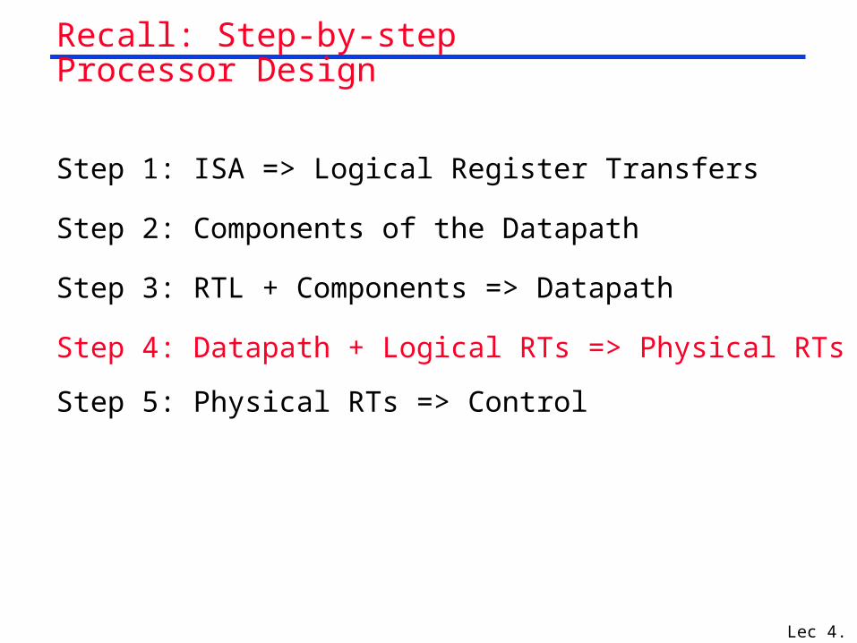
Microprogramming: Designing the control as a program that
implements the machine instructions in terms of microinstructions
PCWritePCWriteCondIorD
MemtoRegPCSourceALUOpALUSrcBALUSrcARegWrite
AddrCtl
Outputs
Microcode memory
IRWrite
MemReadMemWrite
RegDst
Control unit
Input
Microprogram counter
Address select logic
Op[
5–
0]
Adder
1
Datapath
Instruction registeropcode field
BWrite
Microprogramming

Lec 4.46
MainMemory
executionunit
controlmemory
CPU
ADDSUBAND
DATA
.
.
.
User program plus Data
this can change!
AND microsequence
e.g., Fetch Calc Operand Addr Fetch Operand(s) Calculate Save Answer(s)
one of these ismapped into oneof these
Microinstruction ???

Lec 4.47
Microprogramming a Multicycle Processor
1) Choose datapath and sequencer architecture
2) Assign states and sequence of each (multicycle) instruction (i.e., define the controller FSM)
3) Choose microinstruction format (minimum bits to describe all allowable functions of sequencer and datapath)
4) Map instructions into microinstruction sequences

Lec 4.48
Designing a Microinstruction Set
1) Start with list of control signals
2) Group signals together that make sense: called “fields”
3) Place fields in some logical order (e.g., ALU operation & ALU operands first and microinstruction sequencing last)
4) Create a symbolic legend for the microinstruction format, showing name of field values and how they set the control signals
5) To minimize the width, encode operations that will never be used at the same time

Lec 4.49
Multicycle Processor
RegWrite
ALUSrcA
RegDst
PCSource
PCWriteCond
PC
Inst [15-11]
A
B
01
0
14
ALU
ALUOut
Rs
Rw
Rt Registers
Write data
Read data 1
Read data 2
Instruction [31-26]
Instruction [25-21]
Instruction [20-16]
Instruction [15-0]
Instruction register
Address
MemData
Writedata
Memory
MemReadMemWrite
IRWrite
ALUSrcB
ALUOp
2
Ex
ten
de
r
01
16 32
01
MDR
01
IorD
MemtoReg
3
Shift left 2
1 0
PCWrite
Zero
ExtOp
Control
Op [5-0]
ALUControl
Instruction [ 5-0]

Lec 4.50
Microinstruction fieldsField name Value Signals active Comment
Add ALUOp = 00 Cause the ALU to add.ALU control Subt ALUOp = 01 Cause the ALU to subtract; this implements the compare for
branches.Func code ALUOp = 10 Use the instruction's function code to determine ALU control.
SRC1 PC ALUSrcA = 0 Use the PC as the first ALU input.A ALUSrcA = 1 Register A is the first ALU input.B ALUSrcB = 00 Register B is the second ALU input.
SRC2 4 ALUSrcB = 01 Use 4 as the second ALU input.Extend ALUSrcB = 10 Use output of the sign extension unit as the second ALU input.Extshft ALUSrcB = 11 Use the output of the shift-by-two unit as the second ALU input.Read Read two registers using the rs and rt fields of the IR as the register
numbers and putting the data into registers A and B.Write ALU RegWrite, Write a register using the rd field of the IR as the register number and
Register RegDst = 1, the contents of the ALUOut as the data.control MemtoReg = 0
Write MDR RegWrite, Write a register using the rt field of the IR as the register number andRegDst = 0, the contents of the MDR as the data.MemtoReg = 1
Read PC MemRead, Read memory using the PC as address; write result into IR (and lorD = 0 the MDR).
Memory Read ALU MemRead, Read memory using the ALUOut as address; write result into MDR.lorD = 1
Write ALU MemWrite, Write memory using the ALUOut as address, contents of B as thelorD = 1 data.
ALU PCSource = 00 Write the output of the ALU into the PC.PCWrite
PC write control ALUOut-cond PCSource = 01, If the Zero output of the ALU is active, write the PC with the contentsPCWriteCond of the register ALUOut.
jump address PCSource = 10, Write the PC with the jump address from the instruction.PCWrite
Seq AddrCtl = 11 Choose the next microinstruction sequentially.Sequencing Fetch AddrCtl = 00 Go to the first microinstruction to begin a new instruction.
Dispatch 1 AddrCtl = 01 Dispatch using the ROM 1.Dispatch 2 AddrCtl = 10 Dispatch using the ROM 2.

Lec 4.51
State
Op
Adder
1
PLA or ROM
Mux3 2 1 0
Dispatch ROM 1Dispatch ROM 2
0
AddrCtl
Address select logic
Instruction registeropcode field
Sequencer
Dispatch ROM 1Op Opcode name Value
000000 R-format Rformat1
000010 jmp JUMP1000100 beq BEQ1100011 lw Mem1101011 sw Mem1
Dispatch ROM 2Op Opcode name Value
100011 lw LW2101011 sw SW2

Lec 4.52
Microinstructions
Label ALU
controlSRC1 SRC2
Register
control
Memory
PCWrite
controlSequencing
Fetch Add PC 4 Read PC ALU Seq
Add PC Extshft Read Dispatch 1
Fetch and Decode:
R-type instructions
Label ALU
control
SRC1 SRC2Register
controlMemory
PCWrite
controlSequencing
Rformat1
Func code A B Seq
Write ALU Fetch

Lec 4.53
Microinstructions
Label ALU
controlSRC1 SRC2
Register
controlMemory
PCWrite
controlSequencing
Mem1 Add A Exten
d Dispatch 2
LW2 Read ALU Seq
Write MDR Fetch
SW2 Write ALU Fetch
Memory-reference:
Branch
Label ALU
controlSRC1 SRC2
Register
controlMemory
PCWrite
controlSequencing
BEQ1 Subt A B ALUOut - cond Fetch

Lec 4.54
LabelALU
control SRC1 SRC2Register control Memory
PCWrite control Sequencing
Fetch Add PC 4 Read PC ALU SeqAdd PC Extshft Read Dispatch 1
Mem1 Add A Extend Dispatch 2LW2 Read ALU Seq
Write MDR FetchSW2 Write ALU FetchRformat1 Func code A B Seq
Write ALU FetchBEQ1 Subt A B ALUOut-cond FetchJUMP1 Jump address Fetch
Microprogram

Lec 4.55
Summary
Disadvantages of the Single Cycle Processor• Long cycle time
• Cycle time is too long for all instructions except the Load
Multiple Cycle Processor:• Divide the instructions into smaller steps
• Execute each step (instead of the entire instruction) in one cycle
Partition datapath into equal size chunks to minimize cycle time
Follow same 5-step method for designing “real” processor