Embed Size (px)
Citation preview
Rev. 0.1 10/13 Copyright © 2013 by Silicon Laboratories AN798
AN798
EEPROM EMULATION WITH WEAR-LEVELING FOR 8-BIT FLASH MCUS
1. Introduction
This application note demonstrates a way to use the flash memory of an 8-bit flash MCU to emulate single-variable-rewritable EEPROM memory through firmware. The example API provided enables reading and writing ofsingle variables to non-volatile flash memory. The erase-rewrite algorithm implements wear-leveling on the flash bydistributing page erases.
AN568: EEPROM Emulation for Flash Microcontrollers discusses an alternate method for EEPROM emulation.The differences between the method proposed in this document and AN568 are:
1. The firmware implementation included with AN568 requires an update to the sector area whenever a byte is updated. The method described in this document updates the data byte only, which helps with wear leveling.
2. The EEPROM emulation method in this document contains a logical-to-physical mapping, where firmware can access a logical address using the EEPROM interface functions. The EEPROM emulation uses a transition method to read/write flash physical addresses that match the logical addresses. This method has been widely used in NAND flash data management.
3. In the method described in this document, firmware uses byte units to access the EEPROM, just as with a real EEPROM.
2. Relevant Documentation
Silicon Labs 8-bit application notes and software are available on the website: www.siliconlabs.com/8bit-appnotes.
AN568: EEPROM Emulation for Flash Microcontrollers — This document discusses an alternate method for EEPROM emulation.
3. General Theory
3.1. EEPROM and Flash-Based MemoryEEPROM stands for Electrically Erasable Programmable Read-Only Memory and is a type of nonvolatile memorythat is byte erasable. Therefore, it is often used to store small amounts of data that must be saved when power isremoved. The main difference between the flash memory used by the C8051Fxxx MCU families for non-volatiledata storage and EEPROM is the erasable unit size. Flash memory is block-erasable, which means that bytescannot be erased individually. Instead, a block consisting of several bytes (typically 512 or 1024 on the C8051Fxxxdevices) must be erased at the same time. By using firmware, it is possible to emulate individually erasable andrewritable byte memory using block-erasable flash memory.
To provide EEPROM functionality with an 8-bit flash-based MCU in an application, there are many implementationoptions available. A hardware option is to include an external EEPROM module when designing the hardwarelayout of the application. Another is to use the on-chip flash memory and emulate EEPROM functionality through afirmware API. There are some key differences between these two methods:
1. The write access time for flash memory is shorter than for an external EEPROM. This means that writing to emulated EEPROM is faster than writing to an external EEPROM.
2. While a standalone EEPROM will be able to complete a write operation even if the system is reset, the emulated EEPROM will need the CPU to be active throughout the entire flash operation. The consequences of an aborted flash operation should be taken into account when designing an application. The flash-based EEPROM emulation could use checksums and logging to ensure the integrity of written data.
AN798
2 Rev. 0.1
3. The emulated EEPROM will regularly need to erase pages in flash to free space and be able to write to the same page more than once. On a standalone EEPROM, there is no need for a dedicated erase operation, since all bytes can be erased and rewritten independently.
4. The firmware library emulating the EEPROM must also disable interrupts and enable the VDD monitor while performing the flash write/erase operations. With an external hardware EEPROM, interrupts can still occur during the EEPROM-writing process.
3.2. Flash LimitationsFlash memory is limited to a finite number of program-erase cycles. This means that the embedded flash memoryof the MCU can be erased only a certain number of times before the wear will begin to affect the integrity of thestorage. This deterioration applies to all kinds of flash memory. All 8-bit flash MCUs are guaranteed to withstand anumber of erase cycles, which can be found in the data sheet for each device family.
All flash memory is divided into pages, and each page must be erased as a single unit. The amount of on-chip flashmemory and the page size varies from one 8-bit MCU family to another. See the device data sheet for moreinformation about the page size. Because the erase operation erases only whole pages, it is important to write asmuch data as possible to a single page of flash before erasing the page.
AN798
Rev. 0.1 3
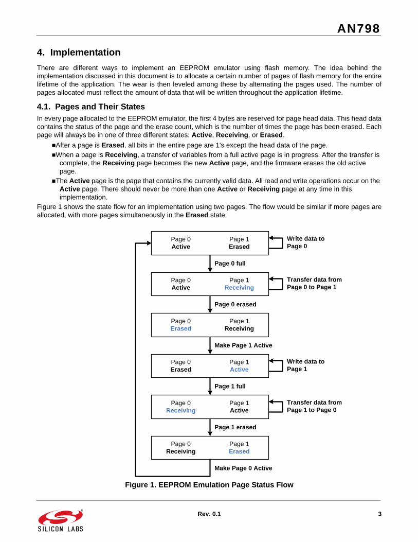
4. Implementation
There are different ways to implement an EEPROM emulator using flash memory. The idea behind theimplementation discussed in this document is to allocate a certain number of pages of flash memory for the entirelifetime of the application. The wear is then leveled among these by alternating the pages used. The number ofpages allocated must reflect the amount of data that will be written throughout the application lifetime.
4.1. Pages and Their StatesIn every page allocated to the EEPROM emulator, the first 4 bytes are reserved for page head data. This head datacontains the status of the page and the erase count, which is the number of times the page has been erased. Eachpage will always be in one of three different states: Active, Receiving, or Erased.
After a page is Erased, all bits in the entire page are 1's except the head data of the page.
When a page is Receiving, a transfer of variables from a full active page is in progress. After the transfer is complete, the Receiving page becomes the new Active page, and the firmware erases the old active page.
The Active page is the page that contains the currently valid data. All read and write operations occur on the Active page. There should never be more than one Active or Receiving page at any time in this implementation.
Figure 1 shows the state flow for an implementation using two pages. The flow would be similar if more pages areallocated, with more pages simultaneously in the Erased state.
Figure 1. EEPROM Emulation Page Status Flow
Page 1 full
Page 1 erased
Page 0Receiving
Page 1Active
Transfer data from Page 1 to Page 0
Make Page 0 Active
Page 0Receiving
Page 1Erased
Page 0 full
Write data to Page 0
Page 0 erased
Page 0Active
Page 1Receiving
Transfer data from Page 0 to Page 1
Page 0Active
Page 1Erased
Make Page 1 Active
Page 0Erased
Page 1Receiving
Page 0Erased
Page 1Active
Write data to Page 1
AN798
4 Rev. 0.1
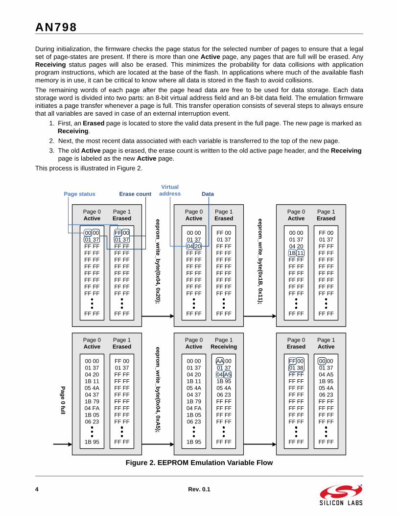
During initialization, the firmware checks the page status for the selected number of pages to ensure that a legalset of page-states are present. If there is more than one Active page, any pages that are full will be erased. AnyReceiving status pages will also be erased. This minimizes the probability for data collisions with applicationprogram instructions, which are located at the base of the flash. In applications where much of the available flashmemory is in use, it can be critical to know where all data is stored in the flash to avoid collisions.
The remaining words of each page after the page head data are free to be used for data storage. Each datastorage word is divided into two parts: an 8-bit virtual address field and an 8-bit data field. The emulation firmwareinitiates a page transfer whenever a page is full. This transfer operation consists of several steps to always ensurethat all variables are saved in case of an external interruption event.
1. First, an Erased page is located to store the valid data present in the full page. The new page is marked as Receiving.
2. Next, the most recent data associated with each variable is transferred to the top of the new page.
3. The old Active page is erased, the erase count is written to the old active page header, and the Receiving page is labeled as the new Active page.
This process is illustrated in Figure 2.
Figure 2. EEPROM Emulation Variable Flow
Page status Erase count
Page 0Active
Page 1Erased
00 0001 3704 20FF FFFF FFFF FFFF FFFF FFFF FFFF FF
FF FF
FF 0001 37FF FFFF FFFF FFFF FFFF FFFF FFFF FFFF FF
FF FF
eepro
m_w
rite_byte(0x04, 0x20);
DataVirtual
address
Page 0Active
Page 1Erased
00 0001 3704 201B 11FF FFFF FFFF FFFF FFFF FFFF FF
FF FF
FF 0001 37FF FFFF FFFF FFFF FFFF FFFF FFFF FFFF FF
FF FF
eepro
m_w
rite_byte(0x1B
, 0x11);
Page 0Active
Page 1Erased
00 0001 3704 201B 1105 4A04 371B 7904 FA1B 0506 23
1B 95
FF 0001 37FF FFFF FFFF FFFF FFFF FFFF FFFF FFFF FF
FF FF
Page 0Active
Page 1Receiving
00 0001 3704 201B 1105 4A04 371B 7904 FA1B 0506 23
1B 95
AA 0001 3704 A51B 9505 4A06 23FF FFFF FFFF FFFF FF
FF FF
eepro
m_w
rite_byte(0x04, 0xA
5);
Page 0Erased
Page 1Active
FF 0001 38FF FFFF FFFF FFFF FFFF FFFF FFFF FFFF FF
FF FF
00 0001 3704 A51B 9505 4A06 23FF FFFF FFFF FFFF FF
FF FF
Page 0Active
Page 1Erased
00 0001 37FF FFFF FFFF FFFF FFFF FFFF FFFF FFFF FF
FF FF
FF 0001 37FF FFFF FFFF FFFF FFFF FFFF FFFF FFFF FF
FF FF
Pag
e 0 full
AN798
Rev. 0.1 5
4.2. Reading and WritingReading consists of iterating through the Active page starting from the end of the page. When the firmware findsthe correct virtual address for the first time, the corresponding data is returned as the currently valid data.
The write operation consists of a similar iteration process starting at the first address of the Active page. When anempty word is found, the firmware writes the correct virtual address and data, and returns. If no empty word isfound, and the end of the page is reached, the page is considered full.
In this implementation, all valid data has to fit inside one Active page. Therefore, the physical flash page size putsa direct limitation on the emulated EEPROM size. Each data slot uses 2 bytes (1 byte for data and 1 byte for thevirtual address), and 4 bytes on the page are reserved for the page status header. By default, the EEPROM size isno more than 1/4 of the flash page size, also considering 8-bit alignment. For example, with a 512-byte flash pagesize, the maximum EEPROM size is:
4.3. Initialization and RecoveryAn important part of EEPROM emulation firmware is to ensure correct page states and enable data recovery onsystem startup. For this reason, the initialization function should be called near the start of the application firmware,before any data is written to or read from the emulated EEPROM. The initializing function decides how many pageswill be allocated to the emulator. The firmware will then check the head of each of these pages to ensure that theset of pages is valid. There are several conditions that should be handled:
Erased page — If an Erased page is not formatted, the firmware will simply format this page. The format operation erases the page and updates the erase count in the page head data.
Pages with Receiving status — The firmware formats this page. This status can be caused by an incomplete page transfer.
Two or more pages with Active status — The firmware compares with two pages and formats any pages that are full.
Once the status check completes, the firmware will scan the current Active page and update the page headinformation.
4.4. Configurable OptionsThe firmware supports all Silicon Labs 8-bit flash MCU families. Define the device being used in theflash_parameters.h file. For example, for a C8051F850 device:
#define C8051F850
The EEPROM emulation firmware has several configurable parameters listed in Table 1. These parameters arelocated in the eeprom_config.h file.
Table 1. Script File Structure
Parameter DescriptionFL_PAGES Pages used for EEPROM emulation: 2
EE_BASE_ADDR EEPROM storage area begins: LOCK_PAGE - FLPAGE_SIZE * FL_PAGES
EE_SIZE EEPROM size in bytes: 16
EE_TAG_SIZE Number of bytes for the page head data: 4
EE_VARIABLE_SIZE Number of bytes used per EEPROM data slot: 2
NMAX512 4–
4------------------- & 0xF8 127 & 0xF8 120= = =

http://www.silabs.com
Silicon Laboratories Inc.400 West Cesar ChavezAustin, TX 78701USA
Simplicity Studio
One-click access to MCU and wireless tools, documentation, software, source code libraries & more. Available for Windows, Mac and Linux!
IoT Portfoliowww.silabs.com/IoT
SW/HWwww.silabs.com/simplicity
Qualitywww.silabs.com/quality
Support and Communitycommunity.silabs.com
DisclaimerSilicon Labs intends to provide customers with the latest, accurate, and in-depth documentation of all peripherals and modules available for system and software implementers using or intending to use the Silicon Labs products. Characterization data, available modules and peripherals, memory sizes and memory addresses refer to each specific device, and "Typical" parameters provided can and do vary in different applications. Application examples described herein are for illustrative purposes only. Silicon Labs reserves the right to make changes without further notice and limitation to product information, specifications, and descriptions herein, and does not give warranties as to the accuracy or completeness of the included information. Silicon Labs shall have no liability for the consequences of use of the information supplied herein. This document does not imply or express copyright licenses granted hereunder to design or fabricate any integrated circuits. The products are not designed or authorized to be used within any Life Support System without the specific written consent of Silicon Labs. A "Life Support System" is any product or system intended to support or sustain life and/or health, which, if it fails, can be reasonably expected to result in significant personal injury or death. Silicon Labs products are not designed or authorized for military applications. Silicon Labs products shall under no circumstances be used in weapons of mass destruction including (but not limited to) nuclear, biological or chemical weapons, or missiles capable of delivering such weapons.
Trademark InformationSilicon Laboratories Inc.® , Silicon Laboratories®, Silicon Labs®, SiLabs® and the Silicon Labs logo®, Bluegiga®, Bluegiga Logo®, Clockbuilder®, CMEMS®, DSPLL®, EFM®, EFM32®, EFR, Ember®, Energy Micro, Energy Micro logo and combinations thereof, "the world’s most energy friendly microcontrollers", Ember®, EZLink®, EZRadio®, EZRadioPRO®, Gecko®, ISOmodem®, Precision32®, ProSLIC®, Simplicity Studio®, SiPHY®, Telegesis, the Telegesis Logo®, USBXpress® and others are trademarks or registered trademarks of Silicon Labs. ARM, CORTEX, Cortex-M3 and THUMB are trademarks or registered trademarks of ARM Holdings. Keil is a registered trademark of ARM Limited. All other products or brand names mentioned herein are trademarks of their respective holders.