Embed Size (px)
Citation preview

Chemical Physics Letters 597 (2014) 1–5
Contents lists available at ScienceDirect
Chemical Physics Letters
journal homepage: www.elsevier .com/ locate /cplet t
Effect of edge states on the transport properties of pentacene–graphenenanojunctions
http://dx.doi.org/10.1016/j.cplett.2014.02.0270009-2614/� 2014 Elsevier B.V. All rights reserved.
⇑ Corresponding author. Fax: +91 3463 262672.E-mail address: [email protected] (P. Sarkar).
Anup Pramanik, Bikash Mandal, Sunandan Sarkar, Pranab Sarkar ⇑Department of Chemistry, Visva-Bharati University, Santiniketan 731235, India
a r t i c l e i n f o
Article history:Received 9 January 2014In final form 14 February 2014Available online 19 February 2014
a b s t r a c t
We investigate the effect of edge states on the transport properties of pentacene–graphene nanojunctionson the basis of DFT and NEGF formalism. The calculations reveal that strong interaction between penta-cene and zigzag GNR leads to edge-induced transmission channels at the Fermi region which controls thelow-bias current. Effects of substitution by electron withdrawing and donating groups on the transportproperties of molecular pentacene have also been discussed, some of which show spin resolved transportproperties with negative differential resistance behavior which may have potential application in spin-tronics devices.
� 2014 Elsevier B.V. All rights reserved.
1. Introduction
In recent years there is a growing interest in the use of organicsemiconductors as the building block of microelectronics or nano-electronics. Pentacene is one such organic semiconductor whichhas shown promise in organic thin-film transistors and having highfield-effect mobility [1–4]. The most attractive features which ledpentacene to be the most useful are its high electron and holemobility, high susceptibility towards thin film formation, andinherent low band-gap owing to its extensive p conjugation andelectron delocalization [2,5,6]. That is why pentacene-basedmolecular junctions, using various metal contacts, have been wide-spread studied both theoretically as well as experimentally andpentacene is considered to be benchmark semiconductor in organ-ic electronic devices. It has also been used to fabricate organicphotovoltaics [7].
During the last couple of years, carbon-based materials such asgraphene, carbon nanotube are proved to serve as better contactmoiety for molecular junctions as they are directly synthesized atthe contact region using chemical vapor deposition and can be pat-terned by lithographic technique [8–11]. Moreover, recentadvances in material growth and control techniques have madegraphene and its 1D ribbon possible to be synthesized in differentorientations. The high conductivity and transparency of grapheneelectrodes have been employed in organic field-effect transistorsand organic photovoltaic solar cells [12–14]. Graphene or few lay-ered graphene electrodes have also been used for electron trans-port through molecular films or molecular junctions [15,16].
Compared to two-dimensional graphene, graphene nanorib-bons (GNRs) are distinct by their electronic and optical properties.The electronic properties of GNRs are sensitive to many factors,edge modification being one of the main control over them[8,17–20]. It has been show that zigzag graphene nanoribbons(zGNRs) exhibit low band-gap semiconducting properties in itsantiferromagnetic ground state [19], while they show halfmetalic-ity under the application of external bias [21,22]. The magnetism inzGNRs is attributed to the peculiar localized states along the zigzagedges [23,24]. There have been extensive researches on the chargeand spin transport properties of zGNR hetero-junctions [25–29]showing negative differential resistance, spin filtering effect etc.,promising them to be useful in magnetoelectronics and spintronicsdevices. Charge transport in pentacene–graphene nanojunctionshas recently been investigated employing density functional the-ory in combination with the Landauer transport formalism [30].The authors have demonstrated how the transport properties areinfluenced by pentacene–graphene coupling pattern and theenergy level sequence. Although the influence of edge states are ta-ken into consideration, they did not resolve the effect of spin chan-nels which is crucial for zigzag edged graphene ribbons.
In this Letter, we have considered the simplest way of penta-cene–graphene nanojunction where the pentacene molecule istrapped between two zigzag nanoribbons to study the effect ofindividual spin channels. Furthermore, the molecular levels ofpentacene have been tuned by the influence of electron donatingor withdrawing functional groups. In order to explore the possibil-ity of practical electronic device application, we have studied thecurrent–voltage characteristics of these nanojunctions. Thus thevarious nanojunctions made of differently functionalized penta-cene show various types of spin resolved transport properties with
2 A. Pramanik et al. / Chemical Physics Letters 597 (2014) 1–5
negative differential resistance behavior which are expected toguide while designing spintronics devices.
2. Model and computation
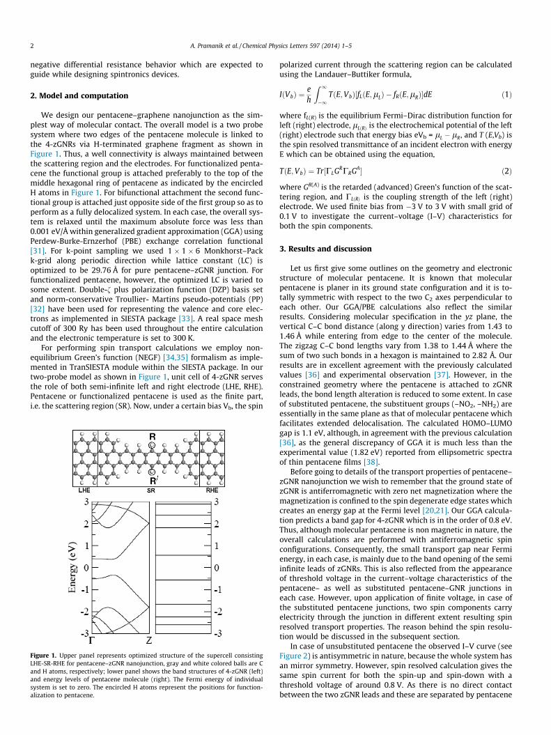
We design our pentacene–graphene nanojunction as the sim-plest way of molecular contact. The overall model is a two probesystem where two edges of the pentacene molecule is linked tothe 4-zGNRs via H-terminated graphene fragment as shown inFigure 1. Thus, a well connectivity is always maintained betweenthe scattering region and the electrodes. For functionalized penta-cene the functional group is attached preferably to the top of themiddle hexagonal ring of pentacene as indicated by the encircledH atoms in Figure 1. For bifunctional attachment the second func-tional group is attached just opposite side of the first group so as toperform as a fully delocalized system. In each case, the overall sys-tem is relaxed until the maximum absolute force was less than0.001 eV/Å within generalized gradient approximation (GGA) usingPerdew-Burke-Ernzerhof (PBE) exchange correlation functional[31]. For k-point sampling we used 1 � 1 � 6 Monkhorst–Packk-grid along periodic direction while lattice constant (LC) isoptimized to be 29.76 Å for pure pentacene–zGNR junction. Forfunctionalized pentacene, however, the optimized LC is varied tosome extent. Double-f plus polarization function (DZP) basis setand norm-conservative Troullier- Martins pseudo-potentials (PP)[32] have been used for representing the valence and core elec-trons as implemented in SIESTA package [33]. A real space meshcutoff of 300 Ry has been used throughout the entire calculationand the electronic temperature is set to 300 K.
For performing spin transport calculations we employ non-equilibrium Green’s function (NEGF) [34,35] formalism as imple-mented in TranSIESTA module within the SIESTA package. In ourtwo-probe model as shown in Figure 1, unit cell of 4-zGNR servesthe role of both semi-infinite left and right electrode (LHE, RHE).Pentacene or functionalized pentacene is used as the finite part,i.e. the scattering region (SR). Now, under a certain bias Vb, the spin
Figure 1. Upper panel represents optimized structure of the supercell consistingLHE-SR-RHE for pentacene–zGNR nanojunction, gray and white colored balls are Cand H atoms, respectively; lower panel shows the band structures of 4-zGNR (left)and energy levels of pentacene molecule (right). The Fermi energy of individualsystem is set to zero. The encircled H atoms represent the positions for function-alization to pentacene.
polarized current through the scattering region can be calculatedusing the Landauer–Buttiker formula,
IðVbÞ ¼eh
Z 1
�1TðE;VbÞ½fLðE;lLÞ � fRðE;lRÞ�dE ð1Þ
where fL(R) is the equilibrium Fermi–Dirac distribution function forleft (right) electrode, lLðRÞ is the electrochemical potential of the left(right) electrode such that energy bias eVb = lL � lR, and T (E,Vb) isthe spin resolved transmittance of an incident electron with energyE which can be obtained using the equation,
TðE;VbÞ ¼ Tr½CLGRCRGA� ð2Þ
where GR(A) is the retarded (advanced) Green’s function of the scat-tering region, and CLðRÞ is the coupling strength of the left (right)electrode. We used finite bias from �3 V to 3 V with small grid of0.1 V to investigate the current–voltage (I–V) characteristics forboth the spin components.
3. Results and discussion
Let us first give some outlines on the geometry and electronicstructure of molecular pentacene. It is known that molecularpentacene is planer in its ground state configuration and it is to-tally symmetric with respect to the two C2 axes perpendicular toeach other. Our GGA/PBE calculations also reflect the similarresults. Considering molecular specification in the yz plane, thevertical C–C bond distance (along y direction) varies from 1.43 to1.46 Å while entering from edge to the center of the molecule.The zigzag C–C bond lengths vary from 1.38 to 1.44 Å where thesum of two such bonds in a hexagon is maintained to 2.82 Å. Ourresults are in excellent agreement with the previously calculatedvalues [36] and experimental observation [37]. However, in theconstrained geometry where the pentacene is attached to zGNRleads, the bond length alteration is reduced to some extent. In caseof substituted pentacene, the substituent groups (–NO2, –NH2) areessentially in the same plane as that of molecular pentacene whichfacilitates extended delocalisation. The calculated HOMO–LUMOgap is 1.1 eV, although, in agreement with the previous calculation[36], as the general discrepancy of GGA it is much less than theexperimental value (1.82 eV) reported from ellipsometric spectraof thin pentacene films [38].
Before going to details of the transport properties of pentacene–zGNR nanojunction we wish to remember that the ground state ofzGNR is antiferromagnetic with zero net magnetization where themagnetization is confined to the spin degenerate edge states whichcreates an energy gap at the Fermi level [20,21]. Our GGA calcula-tion predicts a band gap for 4-zGNR which is in the order of 0.8 eV.Thus, although molecular pentacene is non magnetic in nature, theoverall calculations are performed with antiferromagnetic spinconfigurations. Consequently, the small transport gap near Fermienergy, in each case, is mainly due to the band opening of the semiinfinite leads of zGNRs. This is also reflected from the appearanceof threshold voltage in the current–voltage characteristics of thepentacene– as well as substituted pentacene–GNR junctions ineach case. However, upon application of finite voltage, in case ofthe substituted pentacene junctions, two spin components carryelectricity through the junction in different extent resulting spinresolved transport properties. The reason behind the spin resolu-tion would be discussed in the subsequent section.
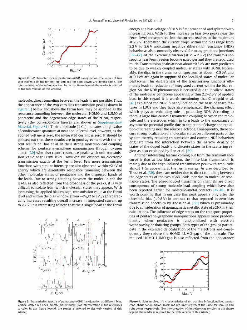
In case of unsubstituted pentacene the observed I–V curve (seeFigure 2) is antisymmetric in nature, because the whole system hasan mirror symmetry. However, spin resolved calculation gives thesame spin current for both the spin-up and spin-down with athreshold voltage of around 0.8 V. As there is no direct contactbetween the two zGNR leads and these are separated by pentacene
-3 -2 -1 0 1 2 3
Bias / V
-30
-20
-10
0
10
20
30
Cur
rent
/ μΑ
Figure 2. I–V characteristics of pentacene–zGNR nanojunction. The values of twospin currents (black for spin-up and red for spin-down) are almost same. (Forinterpretation of the references to color in this figure legend, the reader is referredto the web version of this article.)
A. Pramanik et al. / Chemical Physics Letters 597 (2014) 1–5 3
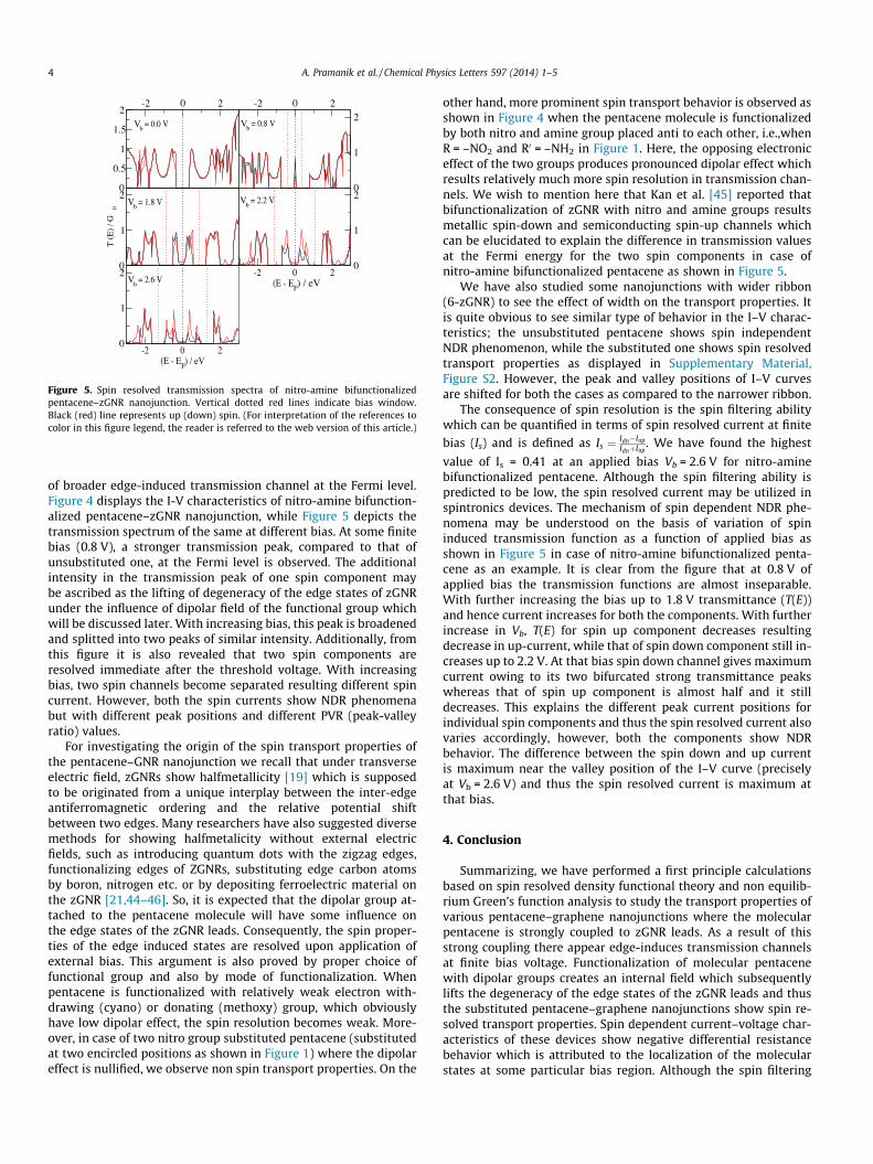
molecule, direct tunneling between the leads is not possible. Thus,the appearance of the two zero bias transmission peaks (shown inFigure 3) below and above the Fermi level may be ascribed as theresonance tunneling between the molecular HOMO and LUMO ofpentacene and the degenerate edge states of the zGNR, respec-tively (the corresponding figures are shown in SupplementaryMaterial, Figure S1). Their amplitude (1 G0) indicates a high valueof conductance quantum at near about Fermi level, however, as theapplied voltage is zero, the integrated current is zero. It should bepointed out that these results are in good agreement with the re-cent results of Thos et al. in their strong molecule-lead couplingscheme for pentacene–graphene nanojunction through oxygenatoms [30] who also report resonance peaks with unit transmis-sion value near Fermi level. However, we observe no electronictransmission exactly at the Fermi level. Few more transmissionfunctions with similar intensity are also observed within ±2 eV ofenergy which are essentially resonance tunneling between theother molecular states of pentacene and the dispersed bands ofthe leads. Due to strong coupling between the molecule and theleads, as also reflected from the broadness of the peaks, it is verydifficult to isolate from which molecular states they appear. Withincreasing the applied bias voltage, transmission value at the Fermilevel and within the bias window (from�eVb/2 to eVb/2) first grad-ually increases resulting overall increase in integrated current upto 2.2 V. It is interesting to note that the a single peak at the Fermi
-2 0 2
0
1
2-2 0 2
0
1
2
0
1
2
T (
E)
/ G
0
-2 0 2(E - E
F) / eV
0
1
2
-2 0 2(E - E
F) / eV
0
1
2
Vb = 0.0 V V
b = 0.8 V
Vb = 2.2 V
Vb = 2.6 V
Vb = 1.5 V
Figure 3. Transmission spectra of pentacene–zGNR nanojunction at different bias.Vertical dotted red lines indicate bias window. (For interpretation of the referencesto color in this figure legend, the reader is referred to the web version of thisarticle.)
energy at a bias voltage of 0.8 V is first broadened and splitted withincreasing bias. With further increase in bias two peaks near theFermi level are separated, but the current reaches to the maximumat 2.2 V. Thereafter, the current drops within the bias range from2.2 V to 2.6 V indicating negative differential resistance (NDR)behavior as also commonly observed for many graphene junctions[39–42]. At the extreme situation (at Vb = 2.6 V) the transmissionspectra near Fermi region become narrower and they are separatedmuch. Transmission peaks at near about ±0.5 eV are now predictedto be due to weakly coupled molecular states with zGNR. Notice-ably, the dips in the transmission spectrum at about �0.5 eV. andat 0.7 eV are again in support of the localized states of molecularpentacene. This discreteness of the transmission functions ulti-mately leads to reduction of integrated current within the bias re-gion. So, the NDR phenomenon is occurred due to localized statesof the molecular pentacene appearing within 2.2–2.6 V of appliedbias. In this regard it is worth mentioning that Cheragchi et al.[43] explained the NDR in nanojunction on the basis of sharp fea-tures in LDOS and they have also emphasized the charging effectwhich plays an enhancing role in producing NDR. According tothem, a large bias causes asymmetric coupling between the mole-cule and the electrodes which in turn leads to the appearance ofasymmetric potential profile due to depletion of charge and reduc-tion of screening near the source electrode. Consequently, there oc-curs strong localization of molecular states on different parts of thesystem thereby reducing transmission and current. NDR behaviorsoriginate from the interaction between the narrow density ofstates of the doped leads and discrete states in the scattering re-gion as also explained by Ren et al. [39].
Another interesting feature coming out from the transmittancecurve is that at low bias region, the finite bias transmission ismainly due to the edge-induced transmission peak with amplitudealmost 1 G0 appearing at the Fermi energy. As also described byThoss et al. [30]. these are neither due to direct tunneling betweenthe edge states of the two zGNR leads, nor due to molecular reso-nance states. The edge-induced transmission channels are directconsequence of strong molecule-lead coupling which have alsobeen reported earlier for molecule–metal contacts [47,48]. It isworth pointing that in our case this peak appears only after thethreshold bias (�0.8 V) in contrast to that reported in zero-biastransmission spectrum by Thoss et al. [30] which is presumablydue to consideration of nonmagnetic metallic state of zGNR in theircalculations. The influence of edge states on the transport proper-ties of pentacene–graphene nanojunctions appears more predom-inantly when pentacene is functionalized with electronwithdrawing or donating groups. Both types of the groups partici-pate in the extended delocalization of the p electrons and conse-quently they reduce the HOMO–LUMO gap of the molecule. Thereduced HOMO–LUMO gap is also reflected from the appearance
-3 -2 -1 0 1 2 3
Bias / V
-30
-20
-10
0
10
20
30
Cur
rent
/ μΑ
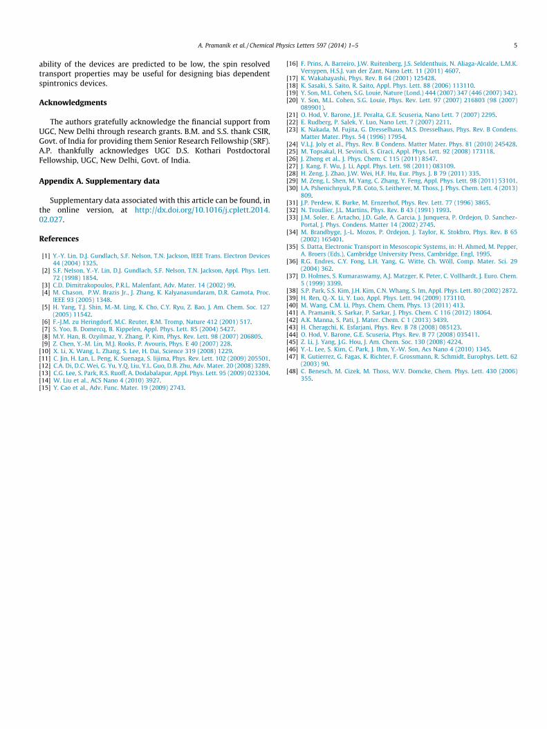
Figure 4. Spin resolved I-V characteristics of nitro-amine bifunctionalized penta-cene–zGNR nanojunction. Black and red lines represent the same for spin-up andspin-down, respectively. (For interpretation of the references to color in this figurelegend, the reader is referred to the web version of this article.)
-2 0 2
0
0.5
1
1.5
2-2 0 2
0
1
2
0
1
2
T (
E)
/ G0
-2 0 2(E - E
F) / eV
0
1
2
-2 0 2(E - E
F) / eV
0
1
2
Vb = 0.0 V V
b = 0.8 V
Vb = 2.2 VV
b = 1.8 V
Vb = 2.6 V
Figure 5. Spin resolved transmission spectra of nitro-amine bifunctionalizedpentacene–zGNR nanojunction. Vertical dotted red lines indicate bias window.Black (red) line represents up (down) spin. (For interpretation of the references tocolor in this figure legend, the reader is referred to the web version of this article.)
4 A. Pramanik et al. / Chemical Physics Letters 597 (2014) 1–5
of broader edge-induced transmission channel at the Fermi level.Figure 4 displays the I-V characteristics of nitro-amine bifunction-alized pentacene–zGNR nanojunction, while Figure 5 depicts thetransmission spectrum of the same at different bias. At some finitebias (0.8 V), a stronger transmission peak, compared to that ofunsubstituted one, at the Fermi level is observed. The additionalintensity in the transmission peak of one spin component maybe ascribed as the lifting of degeneracy of the edge states of zGNRunder the influence of dipolar field of the functional group whichwill be discussed later. With increasing bias, this peak is broadenedand splitted into two peaks of similar intensity. Additionally, fromthis figure it is also revealed that two spin components areresolved immediate after the threshold voltage. With increasingbias, two spin channels become separated resulting different spincurrent. However, both the spin currents show NDR phenomenabut with different peak positions and different PVR (peak-valleyratio) values.
For investigating the origin of the spin transport properties ofthe pentacene–GNR nanojunction we recall that under transverseelectric field, zGNRs show halfmetallicity [19] which is supposedto be originated from a unique interplay between the inter-edgeantiferromagnetic ordering and the relative potential shiftbetween two edges. Many researchers have also suggested diversemethods for showing halfmetalicity without external electricfields, such as introducing quantum dots with the zigzag edges,functionalizing edges of ZGNRs, substituting edge carbon atomsby boron, nitrogen etc. or by depositing ferroelectric material onthe zGNR [21,44–46]. So, it is expected that the dipolar group at-tached to the pentacene molecule will have some influence onthe edge states of the zGNR leads. Consequently, the spin proper-ties of the edge induced states are resolved upon application ofexternal bias. This argument is also proved by proper choice offunctional group and also by mode of functionalization. Whenpentacene is functionalized with relatively weak electron with-drawing (cyano) or donating (methoxy) group, which obviouslyhave low dipolar effect, the spin resolution becomes weak. More-over, in case of two nitro group substituted pentacene (substitutedat two encircled positions as shown in Figure 1) where the dipolareffect is nullified, we observe non spin transport properties. On the
other hand, more prominent spin transport behavior is observed asshown in Figure 4 when the pentacene molecule is functionalizedby both nitro and amine group placed anti to each other, i.e.,whenR = –NO2 and R0 = –NH2 in Figure 1. Here, the opposing electroniceffect of the two groups produces pronounced dipolar effect whichresults relatively much more spin resolution in transmission chan-nels. We wish to mention here that Kan et al. [45] reported thatbifunctionalization of zGNR with nitro and amine groups resultsmetallic spin-down and semiconducting spin-up channels whichcan be elucidated to explain the difference in transmission valuesat the Fermi energy for the two spin components in case ofnitro-amine bifunctionalized pentacene as shown in Figure 5.
We have also studied some nanojunctions with wider ribbon(6-zGNR) to see the effect of width on the transport properties. Itis quite obvious to see similar type of behavior in the I–V charac-teristics; the unsubstituted pentacene shows spin independentNDR phenomenon, while the substituted one shows spin resolvedtransport properties as displayed in Supplementary Material,Figure S2. However, the peak and valley positions of I–V curvesare shifted for both the cases as compared to the narrower ribbon.
The consequence of spin resolution is the spin filtering abilitywhich can be quantified in terms of spin resolved current at finite
bias (Is) and is defined as Is ¼ Idn�Iup
IdnþIup. We have found the highest
value of Is = 0.41 at an applied bias Vb = 2.6 V for nitro-aminebifunctionalized pentacene. Although the spin filtering ability ispredicted to be low, the spin resolved current may be utilized inspintronics devices. The mechanism of spin dependent NDR phe-nomena may be understood on the basis of variation of spininduced transmission function as a function of applied bias asshown in Figure 5 in case of nitro-amine bifunctionalized penta-cene as an example. It is clear from the figure that at 0.8 V ofapplied bias the transmission functions are almost inseparable.With further increasing the bias up to 1.8 V transmittance (T(E))and hence current increases for both the components. With furtherincrease in Vb, T(E) for spin up component decreases resultingdecrease in up-current, while that of spin down component still in-creases up to 2.2 V. At that bias spin down channel gives maximumcurrent owing to its two bifurcated strong transmittance peakswhereas that of spin up component is almost half and it stilldecreases. This explains the different peak current positions forindividual spin components and thus the spin resolved current alsovaries accordingly, however, both the components show NDRbehavior. The difference between the spin down and up currentis maximum near the valley position of the I–V curve (preciselyat Vb = 2.6 V) and thus the spin resolved current is maximum atthat bias.
4. Conclusion
Summarizing, we have performed a first principle calculationsbased on spin resolved density functional theory and non equilib-rium Green’s function analysis to study the transport properties ofvarious pentacene–graphene nanojunctions where the molecularpentacene is strongly coupled to zGNR leads. As a result of thisstrong coupling there appear edge-induces transmission channelsat finite bias voltage. Functionalization of molecular pentacenewith dipolar groups creates an internal field which subsequentlylifts the degeneracy of the edge states of the zGNR leads and thusthe substituted pentacene–graphene nanojunctions show spin re-solved transport properties. Spin dependent current–voltage char-acteristics of these devices show negative differential resistancebehavior which is attributed to the localization of the molecularstates at some particular bias region. Although the spin filtering
A. Pramanik et al. / Chemical Physics Letters 597 (2014) 1–5 5
ability of the devices are predicted to be low, the spin resolvedtransport properties may be useful for designing bias dependentspintronics devices.
Acknowledgments
The authors gratefully acknowledge the financial support fromUGC, New Delhi through research grants. B.M. and S.S. thank CSIR,Govt. of India for providing them Senior Research Fellowship (SRF).A.P. thankfully acknowledges UGC D.S. Kothari PostdoctoralFellowship, UGC, New Delhi, Govt. of India.
Appendix A. Supplementary data
Supplementary data associated with this article can be found, inthe online version, at http://dx.doi.org/10.1016/j.cplett.2014.02.027.
References
[1] Y.-Y. Lin, D.J. Gundlach, S.F. Nelson, T.N. Jackson, IEEE Trans. Electron Devices44 (2004) 1325.
[2] S.F. Nelson, Y.-Y. Lin, D.J. Gundlach, S.F. Nelson, T.N. Jackson, Appl. Phys. Lett.72 (1998) 1854.
[3] C.D. Dimitrakopoulos, P.R.L. Malenfant, Adv. Mater. 14 (2002) 99.[4] M. Chason, P.W. Brazis Jr., J. Zhang, K. Kalyanasundaram, D.R. Gamota, Proc.
IEEE 93 (2005) 1348.[5] H. Yang, T.J. Shin, M.-M. Ling, K. Cho, C.Y. Ryu, Z. Bao, J. Am. Chem. Soc. 127
(2005) 11542.[6] F.-J.M. zu Heringdorf, M.C. Reuter, R.M. Tromp, Nature 412 (2001) 517.[7] S. Yoo, B. Domercq, B. Kippelen, Appl. Phys. Lett. 85 (2004) 5427.[8] M.Y. Han, B. Ozyilmaz, Y. Zhang, P. Kim, Phys. Rev. Lett. 98 (2007) 206805.[9] Z. Chen, Y.-M. Lin, M.J. Rooks, P. Avouris, Phys. E 40 (2007) 228.
[10] X. Li, X. Wang, L. Zhang, S. Lee, H. Dai, Science 319 (2008) 1229.[11] C. Jin, H. Lan, L. Peng, K. Suenaga, S. Iijima, Phys. Rev. Lett. 102 (2009) 205501.[12] C.A. Di, D.C. Wei, G. Yu, Y.Q. Liu, Y.L. Guo, D.B. Zhu, Adv. Mater. 20 (2008) 3289.[13] C.G. Lee, S. Park, R.S. Ruoff, A. Dodabalapur, Appl. Phys. Lett. 95 (2009) 023304.[14] W. Liu et al., ACS Nano 4 (2010) 3927.[15] Y. Cao et al., Adv. Func. Mater. 19 (2009) 2743.
[16] F. Prins, A. Barreiro, J.W. Ruitenberg, J.S. Seldenthuis, N. Aliaga-Alcalde, L.M.K.Versypen, H.S.J. van der Zant, Nano Lett. 11 (2011) 4607.
[17] K. Wakabayashi, Phys. Rev. B 64 (2001) 125428.[18] K. Sasaki, S. Saito, R. Saito, Appl. Phys. Lett. 88 (2006) 113110.[19] Y. Son, M.L. Cohen, S.G. Louie, Nature (Lond.) 444 (2007) 347 (446 (2007) 342).[20] Y. Son, M.L. Cohen, S.G. Louie, Phys. Rev. Lett. 97 (2007) 216803 (98 (2007)
089901).[21] O. Hod, V. Barone, J.E. Peralta, G.E. Scuseria, Nano Lett. 7 (2007) 2295.[22] E. Rudberg, P. Salek, Y. Luo, Nano Lett. 7 (2007) 2211.[23] K. Nakada, M. Fujita, G. Dresselhaus, M.S. Dresselhaus, Phys. Rev. B Condens.
Matter Mater. Phys. 54 (1996) 17954.[24] V.L.J. Joly et al., Phys. Rev. B Condens. Matter Mater. Phys. 81 (2010) 245428.[25] M. Topsakal, H. Sevincli, S. Ciraci, Appl. Phys. Lett. 92 (2008) 173118.[26] J. Zheng et al., J. Phys. Chem. C 115 (2011) 8547.[27] J. Kang, F. Wu, J. Li, Appl. Phys. Lett. 98 (2011) 083109.[28] H. Zeng, J. Zhao, J.W. Wei, H.F. Hu, Eur. Phys. J. B 79 (2011) 335.[29] M. Zeng, L. Shen, M. Yang, C. Zhang, Y. Feng, Appl. Phys. Lett. 98 (2011) 53101.[30] I.A. Pshenichnyuk, P.B. Coto, S. Leitherer, M. Thoss, J. Phys. Chem. Lett. 4 (2013)
809.[31] J.P. Perdew, K. Burke, M. Ernzerhof, Phys. Rev. Lett. 77 (1996) 3865.[32] N. Troullier, J.L. Martins, Phys. Rev. B 43 (1991) 1993.[33] J.M. Soler, E. Artacho, J.D. Gale, A. Garcia, J. Junquera, P. Ordejon, D. Sanchez-
Portal, J. Phys. Condens. Matter 14 (2002) 2745.[34] M. Brandbyge, J.-L. Mozos, P. Ordejon, J. Taylor, K. Stokbro, Phys. Rev. B 65
(2002) 165401.[35] S. Datta, Electronic Transport in Mesoscopic Systems, in: H. Ahmed, M. Pepper,
A. Broers (Eds.), Cambridge University Press, Cambridge, Engl, 1995.[36] R.G. Endres, C.Y. Fong, L.H. Yang, G. Witte, Ch. Wöll, Comp. Mater. Sci. 29
(2004) 362.[37] D. Holmes, S. Kumaraswamy, A.J. Matzger, K. Peter, C. Vollhardt, J. Euro. Chem.
5 (1999) 3399.[38] S.P. Park, S.S. Kim, J.H. Kim, C.N. Whang, S. Im, Appl. Phys. Lett. 80 (2002) 2872.[39] H. Ren, Q.-X. Li, Y. Luo, Appl. Phys. Lett. 94 (2009) 173110.[40] M. Wang, C.M. Li, Phys. Chem. Chem. Phys. 13 (2011) 413.[41] A. Pramanik, S. Sarkar, P. Sarkar, J. Phys. Chem. C 116 (2012) 18064.[42] A.K. Manna, S. Pati, J. Mater. Chem. C 1 (2013) 3439.[43] H. Cheragchi, K. Esfarjani, Phys. Rev. B 78 (2008) 085123.[44] O. Hod, V. Barone, G.E. Scuseria, Phys. Rev. B 77 (2008) 035411.[45] Z. Li, J. Yang, J.G. Hou, J. Am. Chem. Soc. 130 (2008) 4224.[46] Y.-L. Lee, S. Kim, C. Park, J. Ihm, Y.-W. Son, Acs Nano 4 (2010) 1345.[47] R. Gutierrez, G. Fagas, K. Richter, F. Grossmann, R. Schmidt, Europhys. Lett. 62
(2003) 90.[48] C. Benesch, M. Cizek, M. Thoss, W.V. Domcke, Chem. Phys. Lett. 430 (2006)
355.


![Chapter 3 Atmosphere Effect on Pentacene Thin Film Transistors · [56,57] examined the instabilities of the electrical characteristics and the 1/f noise behaviors of pentacene transistors](https://img.pdfslide.net/doc/110x75/5e81a685737a0617625392ec/chapter-3-atmosphere-effect-on-pentacene-thin-film-transistors-5657-examined.jpg)


![Dinaphtho[8,1,2-cde:2',1',8'-uva]pentacene derivative and](https://img.pdfslide.net/doc/110x75/6236a3d2bc5a6b77b25c7a1e/dinaphtho812-cde218-uvapentacene-derivative-and-.jpg)


