Embed Size (px)
Citation preview
Ep
XXZa
b
a
ARRAA
KECPW
1
mcmlmbcwasmo
0h
m.co
m.cn
Applied Surface Science 285P (2013) 469– 476
Contents lists available at ScienceDirect
Applied Surface Science
j ourna l ho me page: www.elsev ier .com/ locate /apsusc
ffect of film compatibility on electro-optic properties of dye dopedolymer DR1/SU-8
iaoqiang Suna,b, Ying Xiea, Xuliang Zhaoa, Dehui Lia, Shimin Zhaoa, Yuanbin Yuea,ibin Wanga, Jian Suna, Lei Lianga, Changming Chena, Daming Zhanga, Fei Wanga,∗,hiyuan Xieb
State Key Laboratory on Integrated Optoelectronics, Jilin University, No. 2699, Qianjin Street, Changchun, Jilin 130012, ChinaChangchun Institute of Applied Chemistry, Chinese Academy of Sciences, No. 5625, Renming Street, Changchun, Jilin 130022, China
r t i c l e i n f o
rticle history:eceived 28 March 2013eceived in revised form 15 August 2013ccepted 19 August 2013vailable online 27 August 2013
eywords:lectro-optic polymersompatibilityassive claddingaveguide
a b s t r a c t
The physic-chemical compatibility of passive cladding and poled Dispersed Red 1 (DR1) doped ultravi-olet (UV) curable polymer SU-8 was investigated. The multilayer films consisting of DR1/SU-8 core andNorland Optical Adhensive 73 (NOA73), SU-8, polydimethylsiloxane (PDMS), or polymethylmethacrylate(PMMA) upper-cladding were fabricated on the silicon substrate, respectively. The interface morpholo-gies were characterized through scan electronic microscope. Parallel plate electric field poling was carriedout to align the polarity of chromophores in SU-8. The core–cladding interface with no chemical erosionor delamination was obtained by adopting an excess UV exposure and higher temperature dealing whenNOA73 was used as the upper-cladding. The root mean square roughness of the upper-cladding surfacewas measured by atomic force microscope to verify the poling process. The electro-optic (EO) signalresponse amplitude of these multilayer films was used to characterize the polarizability alignment ofDR1 chromophores by means of Teng–Man method after poling. Resistivity of claddings was measured
.sp
at the glass transition temperature of DR1/SU-8 to explain the EO response difference. The configura-tion of NOA73/(DR1/SU-8) exhibited the best EO performance and time relaxation in amplitude within550 h by prolonging the cooling time in poling process. A channel waveguide was fabricated to studythe poling-induced optical loss. The results show that the selection of passive cladding with favorableelectrical and chemical property is essential to establish optical nonlinearity in the dye–polymer system.
© 2013 Elsevier B.V. All rights reserved.
www
. Introduction
Electro-optic (EO) polymers are prospective materials withany favorable merits for various applications, including opti-
al network components, on-chip optical interconnects [1–3],icrowave photonics and others [4–6]. They have specialties of
arge EO coefficients, low optical loss at 1.30 and 1.55 �m telecom-unication wavelengths, low dispersion of refractive index (RI)
etween optical frequencies and millimeter waves, easy to pro-ess and relatively low cost. Nonlinear polymers and chromophoresith high molecular polarizability have been designed, tailored
nd introduced from molecular engineering both theoretically and
ynthetically [7–9]. However, most of these materials are not com-ercially available yet. Consequently, these excellent outcomesf molecular engineering are incapable of playing desirable roles
∗ Corresponding author. Tel.: +86 0431 851 680 97; fax: +86 0431 851 680 97.E-mail address: wang [email protected] (F. Wang).
169-4332/$ – see front matter © 2013 Elsevier B.V. All rights reserved.ttp://dx.doi.org/10.1016/j.apsusc.2013.08.079
for the worldwide development of organic EO devices. Amongnonlinear optical systems, guest–host polymers need no chem-ical attachment of chromophores to the host polymer and canbe synthesized at a lower cost than any other systems, includingside-chain, cross-linked, and main-chain polymers that are syn-thesized with more complicated reaction [10–12]. Recently, wehave demonstrated the approach to overcome disadvantages ofguest–host system that fast decay of nonlinear property and lowchromophores concentration by using a high glass transition tem-perature (Tg) host polymer SU-8 doped with organic chromophoresDispersed Red 1 (DR1) that has good miscibility with SU-8 [13].
Practical optical waveguide devices require the active layer tobe sandwiched between two cladding layers [14]. For EO wave-guide, compatible buffer and cladding layers are necessary for lightguiding in the active core. These claddings commonly have char-
acteristics of similar thickness with the active layer, relatively lowoptical loss, and appropriate RI supporting mode propagation [15].Another essential request for the sandwiched layers is to build aneffective poling field through the multilayer geometry to achieve
m
4 ce Science 285P (2013) 469– 476
a[dlwic
cNaeeoAbo
2
2
ws8Dbap
2
ewwpr(aemPDf3fi4t1wipc
2
Dstaphw
uncertainty of input/output coupling loss.
www.sp
70 X. Sun et al. / Applied Surfa
quasi-permanent alignment of polarizability of chromophores16]. Previous studies have shown that effective poling is highlyependent upon factors of voltage division between the multiple-
ayers, chemical and optical characteristics of individual layersith respect to temperature, and chromophore–chromophore
nteraction [17,18]. Thus, favorable core–cladding physic-chemicalompatibility is crucial for polymer EO waveguide fabrication.
In this paper, we report on the investigation of physic-chemicalompatibility of poled dye doped polymer and passive claddings oforland Optical Adhensive 73 (NOA73), SU-8, polydimethylsilox-ne (PDMS) and polymethylmethacrylate (PMMA). We presentxperimental results on the interface morphology through scanlectronic microscope (SEM) and effects of electric field polingn cladding surface roughness by atomic force microscope (AFM).ccording to the measurement of EO signal amplitude and time sta-ility, NOA73 as upper-cladding is more preferable to obtain stableptical nonlinearity and minimal poling-induced optical loss.
. Experiment
.1. EO polymer preparation
To synthesize the EO material, 5 wt% DR1 was doped into theidely used polymer SU-8 2005 (MicroChem Corp.) and thoroughly
tirred to ensure complete mixing. Ultraviolet (UV) curable SU- can realize chemical cross-linking because high absorption ofR1 exists in the UV region and photoacid presents neutralizationecause of the chromophores [13]. To enhance the above processnd reduce chromophores relaxation, 3.5 wt% triarylsulfonium salthotoinitiator was introduced into the EO polymer of DR1/SU-8.
.2. Multilayer sample fabrication
Firstly, the ground electrode of 500 nm aluminum was thermallyvaporated onto the backside of a conductive silicon substrateith a low resistivity of 0.002 � cm. A 5 �m thick DR1/SU-8 filmas formed by spin-coated process on the front side. The sam-le was pre-baked at 65 ◦C for 10 min and 90 ◦C for 20 min toemove the residual solvent. Then, it was UV cured by a mercuryNewport Co., 10 mW/cm2 at 365 nm) lamp for 180 s, followed by
post-exposure baking at 95 ◦C for 15 min and 135 ◦C for 1 h tonhance the cross-linking of EO polymer. Commercialized poly-ers of PMMA (Sigma Aldrich Inc.), NOA73 (Norland Products Inc.),
DMS (Dow Corning Corp.) and SU-8 were spin-coated onto theR1/SU-8 film as the passive upper-cladding and cured under dif-
erent conditions, respectively. PMMA solution was spin-coated at000 rpm and baked at 120 ◦C for 150 min, yielding a 4 �m thicklm. A solvent-free UV curable polymer NOA73 was spin-coated at000 rpm, yielding a 4.5 �m thick film. Then, it was exposed underhe mercury lamp for 170 s and post-exposure baked at 110 ◦C for00 min to enhance cross-linking. Thermal cured PDMS solutionas spin-coated at 2000 rpm and yielding a 2.5 �m thick film. Then,
t was cured at 85 ◦C for 3 h to remove the residual solvent. Theure SU-8 thin film cladding was deposited according to the sameross-linkable process as that of DR1/SU-8.
.3. Electric field poling
Parallel plate electric field poling was used to preferentially alignR1 chromophores and induce a nonzero EO coefficient �33. The
chematic view of experimental setup is shown in Fig. 1. To be prac-ically useful, the poling field was supposed to be as large as possible
nd chosen to be weaker than the dielectric breakdown voltage ofolymers. The substrate temperature was controlled by a lab-madeeater and the temperature controller. Firstly, a field of 100 V/�mas applied to the prepared sample in 25 V steps every 0.1 min at.com
.cn
Fig. 1. Schematic view of experimental setup for parallel plate electric field poling.
room temperature. After the full field was applied, the tempera-ture was raised to Tg (200 ◦C) of DR1/SU-8 at a rate of 15 ◦C/minto avoid decomposition of chromophores [19,20]. The poling fieldwas kept for 30 min at the optimum poling temperature. Once thepoling time was reached, the sample was slowly cooled to roomtemperature to allow the voltage removed without loss of chro-mophores alignment by chilled water coils incorporated into thehotplate [21].
2.4. Waveguide fabrication
A straight channel waveguide was used to study the optical loss.Fig. 2 presents the schematic diagram of fabrication process. Firstly,DR1/SU-8 was spin-coated onto a 3 �m thick silica lower claddingon silicon substrate. After the same material process introducedin Section 2.2, a layer of 100 nm thick aluminum film was ther-mal evaporated onto the top of DR1/SU-8 film as the metal mask.To define waveguide patterns on aluminum film, BP212 photore-sist was spin-coated and patterned by traditional photolithography(ABM Co. Inc., USA) [22]. The oxygen inductively coupled plasmaetching process was performed for 150 s in a 13.56 MHz CE-300I(ULVAC Co. Inc., Japan) etching machine [23,24]. Before the opti-cal loss measurement, the waveguide sample was sliced by a waferdicing machine DAD-3220 (DISCO Co. Inc., Japan) to minimize the
Fig. 2. Schematic diagram of DR1/SU-8 channel waveguide fabrication process.
X. Sun et al. / Applied Surface Science 285P (2013) 469– 476 471
rofile
2
mItwJraItfb
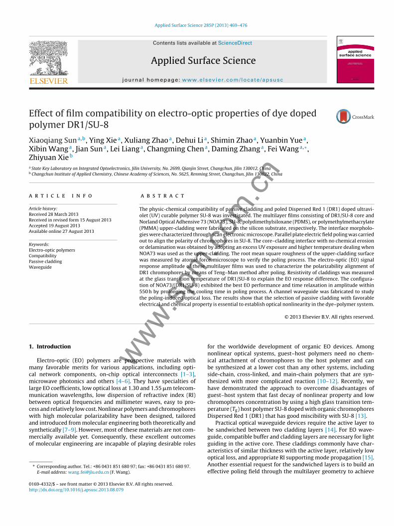
Fig. 3. Temperature, voltage, and current p
.5. Characterization
Refractive indices of DR1/SU-8, NOA73, PDMS, SU-8 and PMMAeasured by spectroscopic ellipsometry M-2000UI (J. A. Woollam
nc., USA) at 1550 nm were 1.57, 1.55, 1.41, 1.56 and 1.48, respec-ively. The characterization of cross-section view of multilayer filmsas examined by means of SEM machine JSM-7600F (JEOL Ltd.,
apan) that operated on voltage of 5 kV. After the top electrode wasemoved from the poled films, AFM images were recorded with
multimode scanning probe microscope CSPM5000 (Being Nano-
www.spmnstrument Ltd., China) that operated in contact mode to measure
he root mean square (RMS) roughness of the upper-cladding sur-ace [25,26]. The EO signal amplitude of poled films was measuredy Teng–Man setup. The output from a tunable semiconductor laser
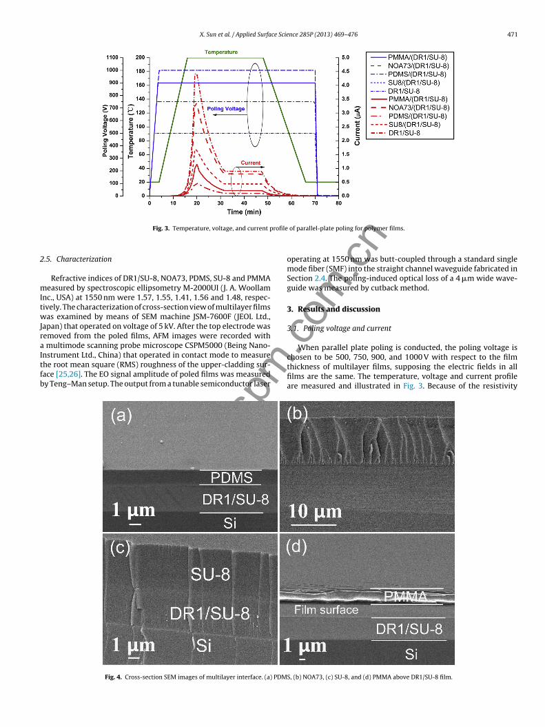
Fig. 4. Cross-section SEM images of multilayer interface. (a) PDM
com
.cn
of parallel-plate poling for polymer films.
operating at 1550 nm was butt-coupled through a standard singlemode fiber (SMF) into the straight channel waveguide fabricated inSection 2.4. The poling-induced optical loss of a 4 �m wide wave-guide was measured by cutback method.
3. Results and discussion
3.1. Poling voltage and current
When parallel plate poling is conducted, the poling voltage is
.chosen to be 500, 750, 900, and 1000 V with respect to the filmthickness of multilayer films, supposing the electric fields in allfilms are the same. The temperature, voltage and current profileare measured and illustrated in Fig. 3. Because of the resistivityS, (b) NOA73, (c) SU-8, and (d) PMMA above DR1/SU-8 film.

m
.cn
472 X. Sun et al. / Applied Surface Science 285P (2013) 469– 476
F 135 ◦C
dcttototcaiecitr
3
raDScweibeptwtD
www.spig. 5. Cross-section SEM images of multilayer interface after 30 s UV exposure and
ifference of claddings, the currents present diverse amplitudehange. As shown in the figure, the current rises quickly withhe decline of polymer resistance which is due to the tempera-ure increasing. A maximum of current appears after about 10 minnce the temperature reached 200 ◦C. With the progress of poling,he disordered chromophores gradually align with the directionf poling field, resulting in an inner electric field reversed withhe direction of outside poling field that leads to the decrement ofurrent. It should be noted the current falls rapidly after the peakppears, which indicates that the rotation of DR1 chromophoress relatively easy. However, this movement gets harder with thestablishment of inner electric field induced by the alignment ofhromophores. After 30 min poling, the current becomes stable,mplying the accomplishment of poling. When multilayer films coolo room temperature, the current almost falls to zero due to theepristination of polymer resistivity.
.2. Interface between layers
The physic-chemical compatibility of core–cladding couples hasemarkable influence on the waveguide fabrication techniquesnd EO performance. Hence, the interface morphology betweenR1/SU-8 film and passive cladding is investigated. Fig. 4 showsEM images of the cross-section view of multilayer films fabri-ated in Section 2.2. A clear interface can be observed in Fig. 4(a)hen PDMS was spin-coated. It proves that DR1/SU-8 film is solid
nough to stand the erosion of cycloheptane solvent in PDMS due tots cross-linking process. No clear interface is observed in Fig. 4(b)ecause of some reason. However, the whole thickness of 10 �mquals the sum of NOA73 and DR1/SU-8 film. Thus, we can sup-ose that this indistinct interface was owing to the close RI of
hese two materials. Blurred borderline is observed in Fig. 4(c),hich implies that inconspicuous dissolution has happened athe interface. This reaction damages the chemical property ofR1/SU-8, especially the orientation stability of chromophores that
.com
baking for 1 h. (a) PDMS, (b) NOA73, (c) SU-8, and (d) PMMA above DR1/SU-8 film.
determines the optical nonlinearity. An obvious delamination canbe observed in Fig. 4(d), which means PMMA cladding does notpossess good adhesion on DR1/SU-8 film. This results in theshrinkage and exposure of underlayer, which is unfavorable forwaveguide cladding application.
To strengthen the physic-chemical stability of multilayer films, afurther 30 s UV exposure and 135 ◦C higher temperature heat deal-ing was adopted to enhance the cross-linking of SU-8. Cross-sectionSEM images of interfaces are shown in Fig. 5, the cladding con-trasts evidently with DR1/SU-8 film. However, an unclear interfaceappears in Fig. 5(a), which may result from the slicing. Comparedwith that in Fig. 5(c), a clearer borderline can be seen in Fig. 5(c),which is owing to the further cross-linking of SU-8. A gap emergesin PMMA cladding, as shown in Fig. 5(d). It indicates that somechemical reaction has happened at the interface, which leads topart of the PMMA cladding peeled off. This is completely unaccept-able for EO waveguide application. Fortunately, a perfect interfaceappears between NOA73 and DR1/SU-8 layer, as shown in Fig. 5(b).To explain this difference, more detailed studies about NOA73 werecarried out. It is found that the viscosity of NOA73 is moderate tobe 140 cps at 25 ◦C that facilitates direct deposition on EO film byspin-coated process. Besides, it does not contain any organic sol-vent, which avoids possible chemical reaction between dye-dopedpolymer and this upper-cladding that would otherwise erode theEO layer.
3.3. Poling effects
The samples were also characterized after poling processintroduced in Section 2.3. Cross-section SEM images of the interfaceare shown in Fig. 6. Compared with state before poling, the inter-
face in Fig. 6(c) is clearer. However, SU-8 cladding becomes fragileand the tenacity decreased, too. This indicates that the physic-chemical property has changed during the high temperature polingprocess. The adhesion problem of PMMA still exists after poling, as
m
.cn
X. Sun et al. / Applied Surface Science 285P (2013) 469– 476 473
ng. (a)
suuiPIef
aT
F
pFig. 6. Cross-section SEM images of multilayer interface after poli
hown in Fig. 6(d). An obvious crack can be seen in this case. Thesenfavorable features destroy the promise of SU-8 and PMMA aspper-cladding in waveguide configuration. Contrastingly, a clear
nterface and flat cross-section can be obtained when NOA73 orDMS was spin-coated on DR1/SU-8, as shown in Fig. 6(a) and (b).t indicates that no certain evidence of chemical erosion or thermalxpansion induced film shrinkage has happened, which is favorableor the alignment of chromophores and reduction of optical loss.
www.sIt has been reported that RMS roughness can characterize thelignment of chromophores with the poling direction [27,28].hus, the cladding surface is measured by AFM before and
ig. 7. AFM images of cladding surface before poling, the RMS roughness is (a) PDMS: 0.33
.com
PDMS, (b) NOA73, (c) SU-8, and (d) PMMA above DR1/SU-8 film.
after poling, as shown in Figs. 7 and 8. For all these multilayer films,the measurement is performed on several samples, and the erroris weighted accordingly. The measurement results show that noRMS roughness is larger than 3 nm, and all cladding surfaces areclean and flat before poling. However, the surface quality changesand RMS roughness increases after poling. It predicates that DR1choromophores have rotated along the poling electric field direc-tion. Moreover, the RMS roughness of cladding surface is different
from each other. This may result from the inner stress that formedinside the multilayer films during poling, which includes the incre-ment and decrease of temperature [29]. Furthermore, according6 nm, (b) NOA73: 2.84 nm, (c) SU-8: 0.767 nm, and (d) PMMA: 2.17 nm, respectively.

m.co
m.cn
474 X. Sun et al. / Applied Surface Science 285P (2013) 469– 476
F : 22.3 nm, (b) NOA73: 18.4 nm, (c) SU-8: 9.55 nm, and (d) PMMA: 14 nm, respectively.
toc
3
asmastotscN
mtrNHasamset
TE
www.spig. 8. AFM images of cladding surface after poling, the RMS roughness is (a) PDMS
o our previous work, this increased roughness may induce excessptical loss that will be discussed in Section 3.4. Thus, a smootherladding surface is more preferable for low loss EO waveguide.
.4. EO characteristic difference
To confirm the EO characteristic of poled polymer, the EO signalmplitudes of DR1/SU-8 film with the above claddings are mea-ured by means of Teng–Man technique at 1 kHz frequency ofodulation electric field [30]. For the dual layer films with both
polymer core and cladding layer, a corrected Teng–Man expres-ion was used to calculate EO coefficient [31]. Here, we just usehe response amplitude to characterize the optical nonlinearityf polymer film. As shown in Table 1, when NOA73 is chosen ashe cladding, the EO signal amplitude is very close to that of theingle DR1/SU-8 film. When SU-8 or PDMS is adopted as upper-ladding, the EO signal amplitude is much smaller than that ofOA73.
This can be explained by the resistivity characteristic of poly-ers that EO core should possess a significantly higher resistance
han that of claddings over the entire range of temperature expe-ienced in poling, from room temperature to Tg. The resistivity ofOA73 or SU-8 at a certain temperature has been reported [32].owever, data quoted in the literature for a given material usu-lly spans several orders of magnitude, depending on factors ofample preparation, degree of polymerization, layer quality, purity,nd others. Thus, the resistivity of polymers used in this study was
easured at the poling temperature of 200 ◦C. To perform this mea-urement, the single polymer film is deposited between two goldenlectrodes as in the case of poling. The sample is placed in the cen-er of a thermostatic container. The applied voltage and electric
able 1O signal amplitude of dual layer films cladding/(DR1/SU-8) before and after poling param
Multilayer film DR1/SU-8 PDM
Poling parameter before optimization (mV) 240 42Poling parameter after optimization (mV) 548 127
Fig. 9. Resistivity of polymers as a function of the applied voltage at 200 ◦C.
current between electrodes are ensured by a high resistance meter(Dongwen, P503, China). According to Eq. (1)
� = V
I
S
t(1)
where V is the potential drop across the polymer layer, S is the areaof the polymer perpendicular to the potential gradient, I is the cur-rent between electrodes, and t is the current path length, resistivity
of cladding and DR1/SU-8 polymer as a function of the applied volt-age can be calculated. The measurement results are shown in Fig. 9.The dual layer films of NOA73/(DR1/SU-8) is expected to display astronger EO response after parallel plate poling than others becauseeter optimization (prolonging the cooling time).
S/(DR1/SU-8) NOA73/(DR1/SU-8) SU-8/(DR1/SU-8)
166 95 358 233

m
X. Sun et al. / Applied Surface Science 285P (2013) 469– 476 475
F
totaiEtota
brlpTutopppoabdNa
m[DiaplosotspD�o
Table 2Optical loss of the channel waveguide before and after poling.
Claddings Before poling(dB/cm)
After poling(dB/cm)
Poling-inducedloss (dB/cm)
NOA73 2.6 3.9 1.3
that excess UV exposure and high temperature dealing can enhance
www.spig. 10. Time relaxation of the EO signal amplitude of multilayer films after poling.
he resistivity NOA73 (3.5 × 10¹¹ � cm) is only a quarter of SU-8,r a third of DR1/SU-8 (9.5 × 10¹¹ � cm). When NOA73 is used ashe cladding material, this low resistivity would allow 72% of thepplied voltage to be dropped across the DR1/SU-8 layer, resultingn high poling field [33]. When PDMS is used as the cladding, theO response amplitude is much lower than that of others becausehe relatively high resistivity 8.6 × 10¹² � cm of PDMS is nearly onerder of magnitude larger than that of DR1/SU-8. Though the filmhickness of PDMS is just one half of that of NOA73, only 17% of thepplied voltage would drop across the DR1/SU-8 layer.
For practical waveguide application, the EO response time sta-ility in multilayer films needs to be confirmed, too. It has beeneported that the thermal stability of the second order optical non-inearity of a poled dye-doped polymer can be improved when thehysical aging temperature coincides with the decay temperature.hus, we prolong the aging time to 2 h to decrease the free vol-me of the polymer matrix and make it more compact aroundhe oriented dopants to hinder the rotation of chromophores outf the alignment [34,35]. The EO signal amplitude after polingarameters optimized is shown in Table 1. Compared with normalrocess, all EO signal amplitude enlarges over two times, whichroves the effectiveness of physical aging to enhance EO responsef this dye-doped UV polymer. The time relaxation of EO signalmplitude was measured periodically to verify the alignment sta-ility [36]. As shown in Fig. 10, all EO responses show magnitudeegradation with time, and become stable after 100 h. Moreover,OA73/(DR1/SU-8) system exhibits the best optical nonlinearitynd time stability amongst these multilayer films.
Since the interaction mechanism between azo dye and hostolecules is different from side chain or main chain EO polymers
37], the time stability comparison is just carried out betweenR1/SU-8 and other DR1 doped guest–host polymers, includ-
ng DR1/poly(bisphenol A carbonate)(PC), DR1/PMMA, DR1/sol–gelnd DR1/poly(2-vinylpyridine)(P2VP). Like other characterizationarameters, such as order parameter, EO coefficient �33 and non-
inear optical coefficient d33 that have been adopted to characterizeptical nonlinearity, EO signal amplitude can be used to prove thetability performance of DR1/SU-8 multilayer films. Normalizedrder parameters of DR1/PC, DR1/PMMA are measured at roomemperature over a period of 24 days in Ref. [38]. They decrease totabilized values after about 10 days. After stabilization, the orderarameter for DR1/PC retains 86% of its original value, while for
R1/PMMA it decays to 69%. Another relaxation measurement of33 for 10% doped DR1/P2VP demonstrates that the EO coefficientnly retains 50% of its original value after 4 days [39]. For DR1.com
.cn
PDMS 1.7 3.8 2.1SU-8 2.8 4.2 1.4
doped sol–gel material, the d value was stable for up to 80 daysat room temperature without initial or long term relaxation [40].Several factors determine the initial order parameter and the ori-entation retention of DR1 molecules, including poling electric fieldand temperature, hydrogen bonding of the hydroxyl group of DR1to carbonyl groups of host polymer, and cladding resistivity. The EOsignal amplitude of DR1/SU-8 reduces 45%, and NOA73/(DR1/SU-8)films reduces 37% from their original values after 10 days. Thoughthe stability performance of NOA73/(DR1/SU-8) films is not thebest, they remained essentially constants for the application in EOwaveguide devices.
3.5. Optical loss
The determination of optical loss lies in the measurement oftransmitted power according to the waveguide length [41]. Astraight channel waveguide was fabricated to study the optical lossintroduced in Section 2.4. The optical loss before and after polingper unit length, measured by cleaving back the waveguide in stepsof 5 mm is shown in Table 2 [42]. The uncertainty of the measure-ment is convinced to be <0.5 dB/cm because of the repeatability ofchip cleaving [43]. As shown in Table 2, the waveguide adoptingPDMS as upper-cladding has the smallest optical loss of 1.7 dB/cmbefore poling. The waveguide adopting NOA73 or SU-8 as upper-cladding exhibits a larger optical loss. Since the upper-cladding RIincrement of from 1.41 to 1.56 is consistent with the sequence ofoptical loss change, we can reasonably reckon that the optical losshas close relationship with the RI contrast between the core andcladding material, which confines the mode field in waveguide. Thehigher the RI contrast is, the more optical power is confined in thecore layer.
After poling, the surface of poled area is exposed by removingthe top electrode. Except for RMS roughness increment revealedin Section 3.3, inhomogeneities regions of several micrometers canbe observed under contrast-enhanced microscope because of theexistence of weak dielectric spots in the cladding layer that affectsthe local poling field. Therefore, the optical loss of samples increasesapparently with the appearance of inhomogeneities in the mediathat are amplified during poling process. Besides, the magnitudeof poling-induced loss is not strictly in accordance to that of the RIsequence. This can be explained by the difference of cladding dielec-tric property and interface morphology between core–claddingcouples after poling. Though the waveguide with PDMS as upper-cladding presents the lowest optical loss of 3.8 dB/cm after poling,the waveguide adopting NOA73 as upper-cladding shows a low-est poling-induced optical loss of about 1.3 dB/cm, which leads toa compromise optical loss of 3.9 dB/cm after poling.
4. Conclusion
In this study, physic-chemical compatibility of passive claddingand guest–host EO polymer DR1/SU-8 was investigated. SEMimages of multilayer films interface morphologies demonstrated
the cross-linking and solidity of DR1/SU-8, preventing it fromchemical erosion and delamination. The measured EO signal ampli-tude and RMS roughness change of the multilayer films surface

m
4 ce Scie
pTmccrsSpa
A
dS(&C2
R
[
[
[
[
[
[
[
[
[
[
[
[
[
[
[
[
[
[
[
[
[
[
[
[
[
[
[
[
[
[
[
[
www.sp
76 X. Sun et al. / Applied Surfa
roved the alignment of DR1 molecules in SU-8 by means ofeng–Man method after parallel plate poling. Resistivity of poly-er claddings indicated the origin of EO response distinction of
ore–cladding couples. The optical nonlinearity and time stabilityan be improved by prolonging cooling time in poling process. As aesult, NOA73 as cladding suggests the low optical loss, strong andtable EO response for DR1/SU-8 waveguide, compared with PDMS,U-8 or PMMA polymers. This series of characterizations in thisaper can be used to find passive claddings with favorable electricalnd chemical property for EO polymer waveguide application.
cknowledgements
This work is supported by the National Natural Science Foun-ation of China (Nos. 61177027, 61107019, 61077041, 61205032),cience and Technology Development Plan of Jilin ProvinceNo. 20110315), Program for Special Funds of Basic Science
Technology of Jilin University (Nos. 201100253, 201103071),hina Postdoctoral Science Foundation (Nos. 2011M500597,012M510900).
eferences
[1] Y. Enami, C.T. Derose, D. Mathine, C. Loychik, C. Greenlee, R.A. Norwood, T.D.Kim, J. Luo, Y. Tian, A.K.-Y. Jen, N. Peyghambarian, Hybrid polymer/sol–gelwaveguide modulators with exceptionally large electro-optic coefficients,Nature Photonics 1 (2007) 180–185.
[2] D.L.K. Eng, S. Kozacik, B.C. Olbricht, S. Shi, D.W. Prather, Broadband low-drivevoltage polymer electro-optic modulator, Proceedings of SPIE 8259 (2012)82590C.
[3] R. Rita Asquini, A. d’Alessandro, A. Salusti, C. Gizzi, Design of a wideband tun-able AWG using electro-optic polymers and push–pull electrode configurationfor ultrafast photonic switching applications, Proceedings of SPIE 5246 (2003)323–332.
[4] W.C. Wang, R. Forber, K. Bui, Compact super wideband optical antenna,Proceedings of SPIE 7316 (2009) 731614.
[5] C.-Y. Lin, A.X. Wang, X. Zhang, B.S. Lee, R.T. Chen, EO-polymer waveguidebased high dynamic range EM wave sensors, Proceedings of SPIE 8258 (2012)82580Y.
[6] L.R. Dalton, D. Lao, B.C. Olbricht, S. Benight, D.H. Bale, J.A. Davies, T. Ewy, S.R.Hammond, P.A. Sullivan, Theory-inspired development of new nonlinear opti-cal materials and their integration into silicon photonic circuits and devices,Optical Materials 32 (2010) 658–668.
[7] L.R. Dalton, Theory-guided design of organic electro-optic materials anddevices, Polymers 3 (2011) 1325–1351.
[8] L.R. Dalton, P.A. Sullivan, D.H. Bale, Electric field poled organic electro-opticmaterials: state of the art and future prospects, Chemical Reviews 110 (2010)22–55.
[9] L.R. Dalton, Theory-inspired development of organic electro-optic materials,Thin Solid Films 518 (2009) 428–431.
10] S.-H. Jang, A.K.-Y. Jen, Polymeric second-order nonlinear optical materials anddevices, in: S.-S. Sun, L.R. Dalton (Eds.), Introduction to Organic Electronicand Optoelectronic Materials and Devices, CRC Press, New York, 2008, pp.467–512.
11] P.A. Sullivan, B.C. Olbricht, L.R. Dalton, Advances in organic materials for opticalmodulation, Journal of Lightwave Technology 26 (2008) 2345–2354.
12] S.-L. Liu, H. Ang, R.-l. Jin, Z.-x. Yan, M.-b. Yi, Electro-optic properties of DR1doped SiO2 organic/inorganic guest–host films, Chemical Research in ChineseUniversities 25 (2009) 726–732.
13] C.M. Chen, X.Q. Sun, D. Zhang, Z.B. Shan, S.-Y. Shin, D.M. Zhang, Dye-doped poly-meric planar waveguide devices based on a thermal UV-bleaching technique,Optics & Laser Technology 41 (2009) 495–498.
14] H. Zhang, D.H. Chang, C. Zhang, C. Wang, W.H. Steier, H.R. Fetterman, Elec-trooptic polymer modulators with an inverted-rib waveguide structure, IEEEPhotonics Technology Letters 15 (2003) 218–220.
15] A.L. Pyayt, Guiding light in electro-optic polymers, Polymers 3 (2011)1591–1599.
16] J.P. Drummond, S.J. Clarson, S. John, F. Zetts, K. Hopkins, S.J. Caracci, Enhancedelectro-optic poling in guest–host systems using conductive polymer-basedcladding layers, Applied Physics Letters 74 (1999) 368–370.
17] M.D. Watson, P.R. Ashley, M. Abushagur, Modeling of optical waveguide pol-ing and thermally stimulated discharge (TSD) charge and current densities
[
[
.com
.cn
nce 285P (2013) 469– 476
for guest/host electro-optic polymers, IEEE Journal of Quantum Electronics 40(2004) 1555–1561.
18] Y.V. Pereverzev, O.V. Prezhdo, L.R. Dalton, Macroscopic order and electro-opticresponse of dipolar chromophore–polymer materials, Chemical Physics andPhysical Chemistry 5 (2004) 1821–1830.
19] C.M. Chen, F. Zhang, H. Wang, X.Q. Sun, F. Wang, Z.C. Cui, D.M. Zhang, UV curableelectro-optic polymer switch based on direct photo definition technique, IEEEJournal of Quantum Electronics 47 (2011) 959–964.
20] H.L. Rommel, B.H. Robinson, Orientation of electro-optic chromophores underpoling conditions: a spheroidal model, Journal of Physical Chemistry C 111(2007) 18765–18777.
21] E.M. McKenna, A.S. Lin, A.R. Mickelson, D. Raluca, Jin, Dan, Comparison of �33
values for AJ404 films prepared with parallel plate and corona poling, Journalof Optical Society of America B 24 (2007) 2888–2892.
22] Y. Zhao, D.M. Zhang, F. Wang, Z.C. Cui, M.B. Yi, C.S. Ma, W.B. Guo, S.Y. Liu, Fabri-cation techniques for polymer/Si optical waveguide, Optics & Laser Technology36 (2004) 657–660.
23] X.Q. Sun, X.D. Li, C.M. Chen, K. Zhang, J. Meng, X.B. Wang, T.F. Yang, D.M. Zhang,F. Wang, Z.Y. Xie, Optimized inductively coupled plasma etching forpoly(methyl-methacrylate-glycidly-methacrylate) optical waveguide, ThinSolid Films 520 (2012) 5946–5951.
24] X. Wang, J. Meng, X. Sun, T. Yang, J. Sun, C. Chen, C. Zheng, D. Zhang, Inductivelycoupled plasma etching to fabricate sensing window for polymer waveguidebiosensor application, Applied Surface Science 259 (2012) 105–109.
25] M. Zenkiewicz, The applications of atom force microscopy in polymer studies,Polimery 44 (1999) 571–578.
26] F. Walther, W.M. Heckl, R.W. Stark, Evaluation of nanoscale roughnessmeasurements on a plasma treated SU-8 polymer surface by atomic forcemicroscopy, Applied Surface Science 254 (2008) 7290–7295.
27] Y.J. Cho, J.-S. Lee, J.-Y. Lee, Synthesis of novel Y-type nonlinear opticalpolyester with enhanced thermal stability of second harmonic generation forelectro-optic applications, Bulletin of the Korean Chemical Society 31 (2010)1509–1514.
28] X.L. Zhang, M. Li, Z.S. Shi, Y. Wan, L.S.H. Zhao, R.L. Jin, X.B. Wang, D.M. Zhang, M.B.Yi, Z.C.H. Cui, Design, synthesis, and characterization of crosslinkable dopedNLO materials based on polyurethanes containing spindle-type chromophores,Macromolecular Chemistry and Physics 212 (2011) 879–886.
29] D. Bosc, A. Maalouf, S. Haesaert, F. Henrio, Investigation into defects occurringon the polymer surface during the photolithography process, Applied SurfaceScience 253 (2007) 6162–6164.
30] C.C. Teng, H.T. Man, Simple reflection technique for measuring the electro-opticcoefficient of poled polymers, Applied Physics Letters 56 (1990) 1734.
31] C.T. DeRose, Ph.D. Dissertation, University of AZ College of Optical Science,2009.
32] S. Michel, J. Zyss, I. Ledoux-Rak, C.T. Nguyen, High-performance electro-opticmodulators realized with a commercial side-chain DR1–PMMA electro-opticcopolymer, Proceedings of SPIE 7599 (2010) 759901.
33] J.G. Grote, J.S. Zetts, R.L. Nelson, F.K. Hopkins, C.H. Zhang, L.R. Dalton, W.H.Steier, Conductive cladding layers for electrode-poled nonlinear optic polymerelectro-optics, Proceedings of SPIE 4114 (2000) 101.
34] Q.S.H. Shen, K.Y. Wong, Improved thermal stability of poled polymers by opti-mized physical aging process, Optics Communications 164 (1999) 47–50.
35] B.F. Yun, G.H. Hu, Ch.G. Lu, Y.P. Cui, Study on dipolar orientation and relaxationcharacteristics of guest–host polymers affected by corona poling parameters,Optics Communications 282 (2009) 1793–1797.
36] D.H. Park, C.H. Lee, W.N. Herman, Analysis of multiple reflection effects inreflective measurements of electro-optic coefficients of poled polymers in mul-tilayer structures, Optics Express 14 (2006) 8866–8884.
37] S.J. Benight, D.H. Bale, B.C. Olbricht, L.R. Dalton, Organic electro-optics: under-standing material structure/function relationships and device fabricationissues, Journal of Materials Chemistry 19 (2009) 7466–7475.
38] F. Wan, G.O. Carlisle, K. Koch, D.R. Martinez, Enhanced second-harmonicresponse and stability of corona-poled guest–host polycarbonate thin films,Journal of Materials Science: Materials in Electronics 6 (1995) 228–234.
39] M.J. Banach, M.D. Alexander Jr., S. Caracci, R.A. Vaia, Enhancement of elec-trooptic coefficient of doped films through optimization of chromophoreenvironment, Chemistry of Materials 11 (1999) 2554–2561.
40] H. Hayashi, H. Nakayama, O. Sugihara, N. Okamoto, Thermally stable and largesecond-order nonlinearity in poled silica films doped with Disperse Red 1 inhigh concentration, Optics Letters 20 (1995) 2264–2266.
41] W. Shi, C.H.S.H. Fang, Q.W. Pan, Z.H.H. Qin, Q.T. Gu, D. Xu, J.Z.H. Yu, Optimiza-tion and characterization of the guest–host polyetherketone polymer films forapplication in integrated optical devices, Journal of Physics D: Applied Physics35 (2002) 1404.
42] B. Yang, L. Yang, R. Hu, Z. Sheng, D. Dai, Q. Liu, S. He, Fabrication and charac-terization of small optical ridge waveguides based on SU-8 polymer, Journal ofLightwave Technology 27 (2009) 4091–4096.
43] H.-M. Lee, M.-C. Oh, H. Park, W.-Y. Hwang, J.-J. Kim, End-face scattering loss inintegrated-optical waveguides, Applied Optics 36 (1997) 9021–9024.