Embed Size (px)
Citation preview

EFFECT OF SUBSTARTE PARASITICS ON
HETEROJUNCTION BIPOLAR TRANSISTORS A THESIS SUBMITTED IN PARTIAL FULFILLMENT OF THE REQUIREMENTS
FOR THE DEGREE OF
BACHELOR IN TECHNOLOGY
IN
ELECTRONICS AND COMMUNICATION ENGINEERING
By
ASIS PANIGRAHI
ROLL NO-10609010
AND
MONALISHA MOHANTY
ROLL NO-10609029
Under the guidance of
Prof. NVLN MURTHY
DEPARTMENT OF ELECTRONICS & COMMUNICATION ENGINEERING
NATIONAL INSTITUTE OF TECHNOLOGY
ROURKELA
2006-2010

C E R T I F I C A T E
This is to certify that the thesis entitled, “EFFECT OF SUBSTRATE PARASITIC ON
HETEROJUNCTION BIPOLAR TRANSISTOR” submitted by ASIS PANIGRAHI (ROLL
NO-10609010) AND MONALISHA MOHANTY (ROLL NO-10609029) in partial fulfillment of the requirement for the award of BACHELOR OF TECHNOLOGY degree in
ELECTRONICS AND COMMUNICATION ENGINEERING at NATIONAL INSTITUTE OF TECHNOLOGY,ROURKELA is an authentic work carried out by them under my supervision and guidance.
To the best of my knowledge, the matter embodied in the thesis has not been submitted to any
other university /institute for the award of any degree or diploma.
Date:
Prof.NVLN MURTHY (Supervisor) Place: Dept. of E&CE
National Institute of Technology ROURKELA
ACKNOWLEDGEMENTS
First of all, I would like to express my deep sense of respect and gratitude towards my
advisor and guide Prof. NVLN MURTHY, who has been the guiding force behind this
work. I am greatly indebted to him for his constant encouragement, invaluable advice and
for propelling me further in every aspect of my academic life. His presence and optimism
have provided an invaluable influence on my career and outlook for the future. I consider
it my good fortune to have got an opportunity to work with such a wonderful person.
I would like to thank all faculty members and staff of the Department of
Electronics and Communication Engineering, N.I.T. Rourkela for their generous help in
various ways for the completion of this thesis.
ASIS PANIGRAHI
ROLL NO-10609010
MONALISHA MOHANTY
ROLL NO-10609029

CONTENTS
ABSTRACT
Chapter 1- Introduction : HETEROJUNCTION BIPOLAR TRANSISTOR
1.1.Heterojunction
1.2.Application of Heterojunction 1.3.Heterojunction Bipolar Transistor(HBT)
1.4.Various Compound Semiconductor Technology For HBT
1.5.Strained layer of SiGe Alloy
1.6.DC Characteristics of HBT
1.7.Frequency Response Of HBT 1.8.Effect of Temperature On HBT
1.9.How SiGe HBTs are More Advanced Than Si
1.10.Key Features Of Fabrication Of SiGe HBT
Chapter 2-Effect Of Substrate Parasitic On SiGe HBT
Amplifier 2.1.Substrate Parasitic Effects On Gain Relation Between HBT In
CB And CE Mode
2.2.Small Signal Analysis Of SiGe HBT
2.3.Circuit Analysis Of HBT in CB And CE Mode
2.4.Simulation Results
2.5.Conclusion

Chapter 3- Effect Of Substrate Parasitic On SiGe HBT Oscillator
3.1.Analysis Of SiGe HBT In CB Mode Without Considering Substrate Parasitic
3.2. Analysis Of SiGe HBT In CB Mode With Considering
Substrate Parasitic
3.3.Analysis Of SiGe HBT In CE Mode Without Considering
Substrate Parasitic 3.4.Analysis Of SiGe HBT In CE Mode With Considering
Substrate Parasitic
3.5.Conclusion

ABSTRACT
Though the semiconductor silicon(Si) has been used to manufacture the integrated circuits, it I
for the manufacturing of high speed and high frequency circuits. In order to improve the
performance of Si transistors enough to be competitive with III-V devices for RF and
microwave application, while preserving the yield cost and manufacturing advantages associated
with conventional Si fabrication, silicon-germanium(Si-Ge) hetero junction bipolar transistor has
been introduced. SiGe HBTs can provide faster switching speeds than Si bipolar transistors
mainly because of reduced base resistance and collector-to-substrate capacitance.
Analyzing the small signal model of SiGe HBT, we computed its s parameters and plotted it in
smith chart to a frequency variation of 1-18GHz. Again we analyzed the circuit while taking the
external parasitic effect into account and drew the S-parameters in a smith chart. So, in this
frequency range we compared the performance of the device with and without taking the external
substrate effect into account.
We drew the graph for maximum available power gain of common emitter SiGe HBT , with and
without taking the substrate parasitic effect. We compared the graph in both the cases and
verified that the maximum available power gain decreases considerably due to the external
substrate effect. We also verified the substrate effect in case of common base SiGe HBT and saw
that, in this case also the maximum available power gain decreases due to the external substrate
effect.
By plotting graph we verified that,if we don’t consider the substrate parasitic effects then the
gain of SiGe HBT in CB mode is much higher than that of in CE mode. But inclusion of parasitic
degrades the superior power gain of HBT in CB mode and hence its gain reduces than that of in
CE mode
Grounding the substrate is an effective way to reduce the effects of substrate parasitic on SiGe
HBT used as an amplifier. We verified this, by plotting the graph of maximum available power

gain of common base and common emitter SiGe HBT while grounding the substrate and
comparing it with while not grounding the substrate.
Again we designed microwave oscillator using common base and common emitter SiGe HBT
and saw how the oscillation frequency has been decreased due the substrate parasitic effect in
both the cases.

CHAPTER 1
INTRODUCTION :
HETEROJUNCTION
BIPOLAR TRANSISTOR

HETEROJUNCTION :
A hetero junction is the interface that occurs between two layers or regions of dissimilar
crystalline semiconductors. These semiconducting materials have unequal band gaps as
opposed to a homo junction.
• Energy bandgap(in ev) of different hetero junction semiconductors are GaAs= 1.43
AlAs=2.16 GaP=2.21 InAs= 0.36 InP=1.35 Si= 1.11 Ge =0.66. [1]
• Each of the above material is made up of a crystal lattice whose electrical properties
depend on a periodic arrangement of atoms. This periodicity is broken at the hetero
junction interface to varying degrees. In cases where both materials have the same
lattice, they may still have differing lattice constants which give rise to crystal strain
which changes the band energies.
Fig 1.1-Comparision of energy band diagram of an HBT and a BJT
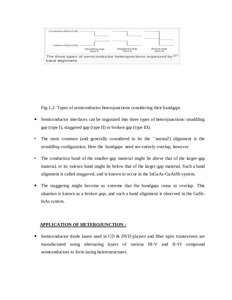
Fig-1.2- Types of semiconductor heterojunctions considering their bandgaps
Semiconductor interfaces can be organized into three types of heterojunctions: straddling
gap (type I), staggered gap (type II) or broken gap (type III).
• The most common (and generally considered to be the ``normal') alignment is the
straddling configuration. Here the bandgaps need not entirely overlap, however.
• The conduction band of the smaller-gap material might lie above that of the larger-gap
material, or its valence band might lie below that of the larger-gap material. Such a band
alignment is called staggered, and is known to occur in the InGaAs-GaAsSb system.
The staggering might become so extreme that the bandgaps cease to overlap. This
situation is known as a broken gap, and such a band alignment is observed in the GaSb-
InAs system.
APPLICATION OF HETEROJUNCTION :
Semiconductor diode lasers used in CD & DVD players and fiber optic transceivers are
manufactured using alternating layers of various III-V and II-VI compound
semiconductors to form lasing heterostructures.

Heterojunctions are used in high electron mobility transistors (HEMT) which can
operate at significantly higher frequencies (over 500 GHz).
HETEROJUNCTION BIPOLAR TRANSISTOR (HBT) :
• The principal difference between the BJT and HBT is in the use of differing
semiconductor materials for the emitter and base regions, creating a heterojunction.
NEED FOR HBT:
The carrier mobility for both electrons and holes in Si is small, and the maximum
velocity that these carriers can attain is limited to about 10,0000 m/sec.
As Si is an indirect gap semiconductor, light emission is painfully inefficient, making
optical devices such as lasers impractical.
Poorer intrinsic speed for si becomes problematic especially when operated in
microwave frequency range.
VARIOUS COMPOUND SEMICONDUCTOR TECHNOLOGY FOR HBT :
Materials used for the substrate include silicon, gallium arsenide, and indium phosphide,
while silicon / germanium alloys, aluminium gallium arsenide/ gallium arsenide, and
indium phosphide/ indium gallium arsenide are used for the epitaxial layers.
Wide-bandgap semiconductors are especially promising, eg. Gallium nitride and indium
gallium nitride.These are also called III-V compound semiconductors.
III-V devices have higher mobility , high saturation velocity which is suitable for high
speed devices.
Due to their direct band gap nature they make excellent optical devices.

But due to its lower levels of integration, poorer heat conduction,more difficult
fabrication, lower yield, and higher cost , it cant be used in the mainstream for the
manufacturing if ICs.
Fig-1.3-Energy Band Diagram Of a Graded Base SiGe HBT Compared to an Si BJT
EVOLUTION OF SiGe HBT TECHNOLOGY :
As Ge has a larger lattice constant than Si, the energy bandgap of Ge is smaller than that
of Si (0.66 eV versus 1.12 eV), and we thus expect SiGe to have a bandgap smaller than
that of Si, making it a suitable candidate for bandgap engineering than Si.
STRAINED LAYER OF SiGe ALLOY :
Si and Ge can be combined to produce a chemically stable alloy (“SiGe”), their lattice
constants differ by roughly 4% and, thus, SiGe alloys grown on Si substrates are
compressively strained. (This is referred to as “pseudomorphic” growth of SiGe on
Si).
These SiGe strained layers are subject to a fundamental stability criterion limiting their
thickness for a given Ge concentration.

Fig-1.4 Film stability space showing effective thickness as a function of effective strain for SiGe
films grown on Si
The compressive strain associated with SiGe alloys produces an additional bandgap
shrinkage, and the net result is a bandgap reduction of approximately 7.5 meV for each
1% of Ge introduced.
The compressive strain lifts the conduction and valence band degeneracies at the band
extremes, effectively reducing the density of states and improving the carrier mobilities
with respect to pure Si.
Since the SiGe film has to be thin if it is to be remain stable , it is used in the base region
of a bipolar transistor.
The resultant device contains an n-Si/p-SiGe emitter–base (EB) heterojunction and a p-
SiGe/n-Si base–collector heterojunction.
The extrinsic resistive and capacitive parasitics are intentionally minimized to improve
the maximum oscillation frequency of the transistor.

The boron-doped graded SiGe base is deposited across the entire wafer using the
UHV/CVD technique .
The deposited layer is polycrystalline (poly), and will serve either as the extrinsic base
contact of the SiGe HBT or the gate electrode of the Si CMOS devices .
The Ge profile is graded across natural base.
The peak Ge content in typical profiles ranges from 8% to 15% and are
thermodynamically stable as grown. The metallurgical base and single-crystal emitter
widths ranges from 75 to 90 nm and 25 to 35 nm.
DC CHARACTERISTICS :
Fig-1.5-comparision of the collector and base currents as a function of EB voltage for an
SiGe HBT and an Si BJT of comaparable doping profile
The Ge- induced band offset exponentially decreases the intrinsic carrier density in the
base which, in turn, decreases the base resistance and, hence, increases Jc.

In the graded-base design, the emitter region of the SiGe HBT and Si BJT comparison
are essentially identical, implying that the resultant base current density(Jb) of the two
transistors will be roughly the same. The net result is that the introduction of Ge increases
the current gain of the transistor.(β=Jc/Jb).
Injection efficiency is defined as the ratio between (electron current injected from
emitter to base) and (hole current injected from base to emitter).High injection efficiency
is obtained in HBT by having a larger bandgap for the emitter than the base.
FREQUENCY RESPONSE :
An important figure of merit in bipolar transistors is the unity-gain cut off frequency(Ft)
given by:
Ft=1/{1/Gm(Ceb+Ccb)+Tb,Tc,Te}
where Gm is the transconductance, and Ceb,Ccb are the EB and CB capacitances, and
Te,Tb,Tc are the base, emitter and collector transit times respectively.
Out of the above parameters Tb typically limits maximum Ft of the transistor. The built-
in electric field induced by the Ge grading across the neutral base effectively decreases
since, physically, the carriers are more rapidly accelerated across the base.
The maximum oscillation frequency (Fmax), is a more relevant figure of merit for
practical RF and microwave applications since it also depends on the parasitics of the
device and as it is directly proportional to Ft we get an improved frequency response by
increased oscillation frequency.

Fig1.6- Comparision of cut off frequency as a function of bias current for an SiGe HBT
and Si BJT of comparable doping profile
EFFECTS OF TEMPERATURE :
Fig-1.7- Cut off frequency as a function of bias current at 300k and 85k for an SiGe HBT

Bandgap engineering generally has a very positive influence on the temperature
characteristics of SiGe HBT’s and thus allows the SiGe HBT to operate well in the
cryogenic environment (e.g., liquid-nitrogen temperature 77 K), a regime which is
traditionally forbidden to Si BJT’s.
The proper choice for the Ge profile shape can yield an SiGe HBT which has a β with
zero temperature coefficient a decided advantage for many circuit applications especially
in the temperature range -55c to -125c.
HOW SiGe HBTs ARE MORE ADVANCED THAN Si : [1]
Higher cut-off frequency due to lower transit time and lower base resistance(as base
doping concentration is high).
Higher gain(beta)and early voltage product and hence better intrinsic device linearity.
Very low collector-substrate capacitance(Ccs) due to the use of semi insulating substrate
and hence improved frequency response.
Extremely good wide band impedance matching due to the resistance nature of input and
output impedance.
Improved lithographic yield lower fabrication cost as there is no need for electron beam
lithography.
High injection efficiency is obtained by using a material with a larger bandgap for the
emitter than that of base.
They offer higher breakdown voltage and high power added efficiency.
KEY FEATURES OF FABRICATION OF SiGe HBT : [1]
Film uniformity and control for both doping, Ge content,film thickness, and Ge profile
shape must be excellent(e.g.,< 5 % variation across the wafer) on large Si wafers.
Film contaminants (e.g.,C andO) must be miniscule with excellent interface quality
between the epi layer and the underlying substrate.
Growth conditions (i.e., rate and temperature) must allow very abrupt doping transitions
with large dynamic range.
Batch wafer processing for high wafer throughput is highly desirable.

CHAPTER 2
EFFECTS OF SUBSTRATE PARASITICS
ON SiGe HBT AMPLIFIER
SUBSTRATE PARASITIC EFFECTS ON GAIN RELATION BETWEEN CE & CB SiGe
HBT :
SiGe HBTs of recent generations have begun to employ higher Ge concentrations and much higher doping concentrations in the base region than the earlier generations in order to improve fmax (power gain) and balance the significantly
improved (Ft) that is resulted from vertical structure downscaling and optimizations . A direct consequence of the engineering efforts is significantly reduced base
resistance.[2]
The reduced base resistance significantly boosts the power gain of common-base (CB) SiGe HBTs and can make their power gain in various frequency ranges
higher than that of common-emitter (CE) SiGe HBTs.[2]
If we consider SiGe power HBTs with large emitter area (multiple emitter fingers) the interconnect parasitic are stronger than low-power devices.[2]
However, the substrate coupling (including probing pad parasitic ) between input and output of these power devices are not significant.[2]
In most cases, there is no need to de-embed the pad parasitic for device characterization and analysis. The power gain relation between the CE and the CB
configurations of these large-size devices is consistent with their intrinsic power gain relation as long as the device size are not so huge such that the total emitter- interconnect and the total base- interconnect metal resistance become
dominant over the intrinsic emitter and base resistance.[2]
For devices with single or a few emitter fingers, although their interconnect
parasitic are not significant, the parasitic introduced by substrate can be very significant.[2]
Moreover, the intrinsic power gain relation between CE and CB configurations may change due to the substrate parasitic effects when the device size is small.[2]

A. Intrinsic Power Gain
The intrinsic devices are referred to the active devices that are not associated with any interconnect or substrate parasitic.[2].
The devices have single emitter finger, double base and double collector fingers in
both CE and CB configurations. These devices are high breakdown voltage devices.[2]
Fig-2.1- Intrinsic power gain relation between CE and CB configuration of single emitter
finger SiGe HBTs
The superior power gain of the CB configuration is the result of low base resistance of the devices.

B. Power Gain with Parasitics
Fig-2.2- Power gain relation between CE and CB configuration of single emitter finger
SiGe HBTs considering substrate parasitic
Compared with Fig. it is found that the CE/CB intrinsic power gain relation is lost with the inclusion of parasitics. The power gain of the CE configuration
almost maintains as shown in Fig(without little effects of parasitics), while the CB power gain degrades much more than CE.[2]
Because of the effects of parasitics, the superior power gain of the CB
configuration is vanished, even though it is intrinsically very hig. In average, the power gain of the CB configuration is reduced by more than 10dB.[2]

Fig-2.3- Equivalent circuit model of CB SiGe HBT with pad and substrate
parasitic. Input is emitter (E) and output is collector (C).
Fig-2.4- Small-signal equivalent circuit of the CB (EBC: 122) SiGe HBT with
substrate parasitic. Cpx combines the effect of Ccs and Ces in Fig.2.3
To break the coupling between input and output through substrate, the substrate is
grounded in order to reduce the substrate parasitic effects.
The power gain of the CB SiGe HBT is greatly enhanced in comparison to gain where the substrate is not grounded. Hence well-grounding the substrate is an
effective way to reduce the substrate parasitic effects and can help maintain the superior power gain of CB configuration SiGe HBTs.

Fig-2.5- Comparison of the enhanced power gain with the intrinsic power gain of
HBT in CB mode
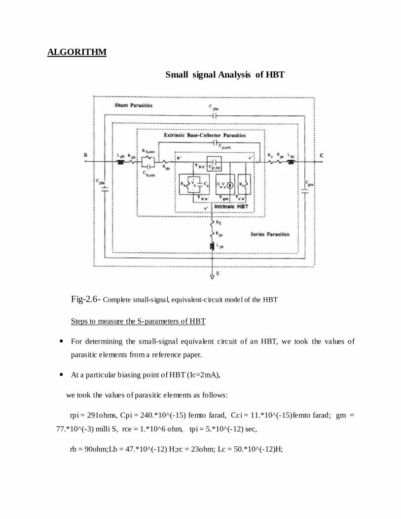
ALGORITHM
Small signal Analysis of HBT
Fig-2.6- Complete small-signal, equivalent-circuit model of the HBT
Steps to measure the S-parameters of HBT
For determining the small-signal equivalent circuit of an HBT, we took the values of
parasitic elements from a reference paper.
At a particular biasing point of HBT (Ic=2mA),
we took the values of parasitic elements as follows:
rpi = 291ohms, Cpi = 240.*10^(-15) femto farad, Cci = 11.*10^(-15)femto farad; gm =
77.*10^(-3) milli S, rce = 1.*10^6 ohm, tpi = 5.*10^(-12) sec,
rb = 90ohm;Lb = 47.*10^(-12) H;rc = 23ohm; Lc = 50.*10^(-12)H;

re = 30ohm; Le = 12.*10^(-12)H;
Divide the whole circuit into 4blocks:
Intrinsic HBT, Base, collector and emitter
Find out the ABCD-parameters of Intrinsic HBT, Base and collector .Since these 3
blocks are in cascaded form, the ABCD parameters of these blocks will be multiplied.
Then transform the ABCD-parameters into Z-parameter. The resulting block is in series
with the emitter block. So add the Z-parameters of these two blocks.
Now transform the Z-parameter into its equivalent S-parameter and draw the S-
parameters in a smith chart with respect to the variation of frequency from 1GHz-18GHz.

SIMULATION RESULT
SMITH CHART

POLAR CHART

TRANSDUCER POWER GAIN

MAXIMUM AVAILABLE GAIN
Gmax: It is defined as the maximum gain of an amplifier circuit when the input
impedance and output impedance are matched.
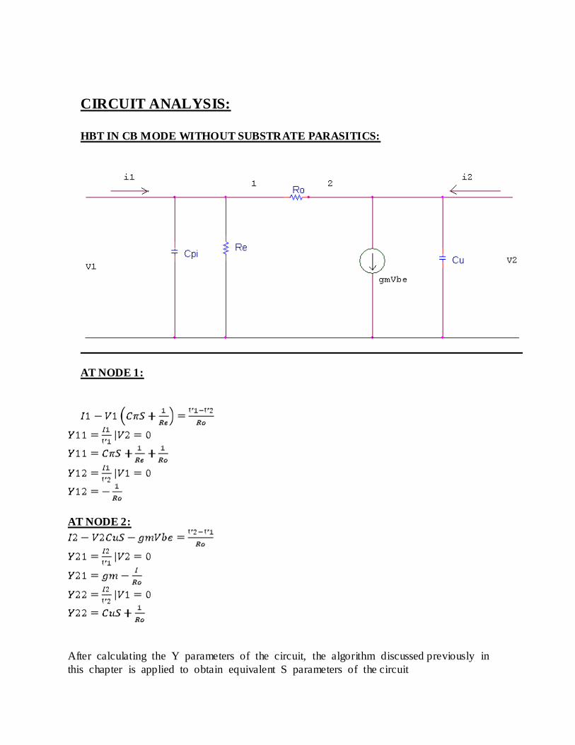
CIRCUIT ANALYSIS:
HBT IN CB MODE WITHOUT SUBSTRATE PARASITICS:
AT NODE 1:
AT NODE 2:
After calculating the Y parameters of the circuit, the algorithm discussed previously in
this chapter is applied to obtain equivalent S parameters of the circuit
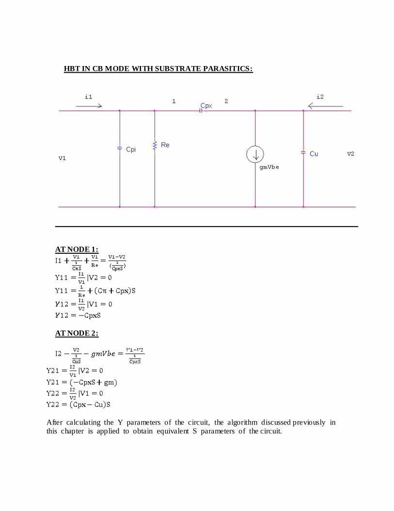
HBT IN CB MODE WITH SUBSTRATE PARASITICS:
AT NODE 1:
AT NODE 2:
After calculating the Y parameters of the circuit, the algorithm discussed previously in this chapter is applied to obtain equivalent S parameters of the circuit.
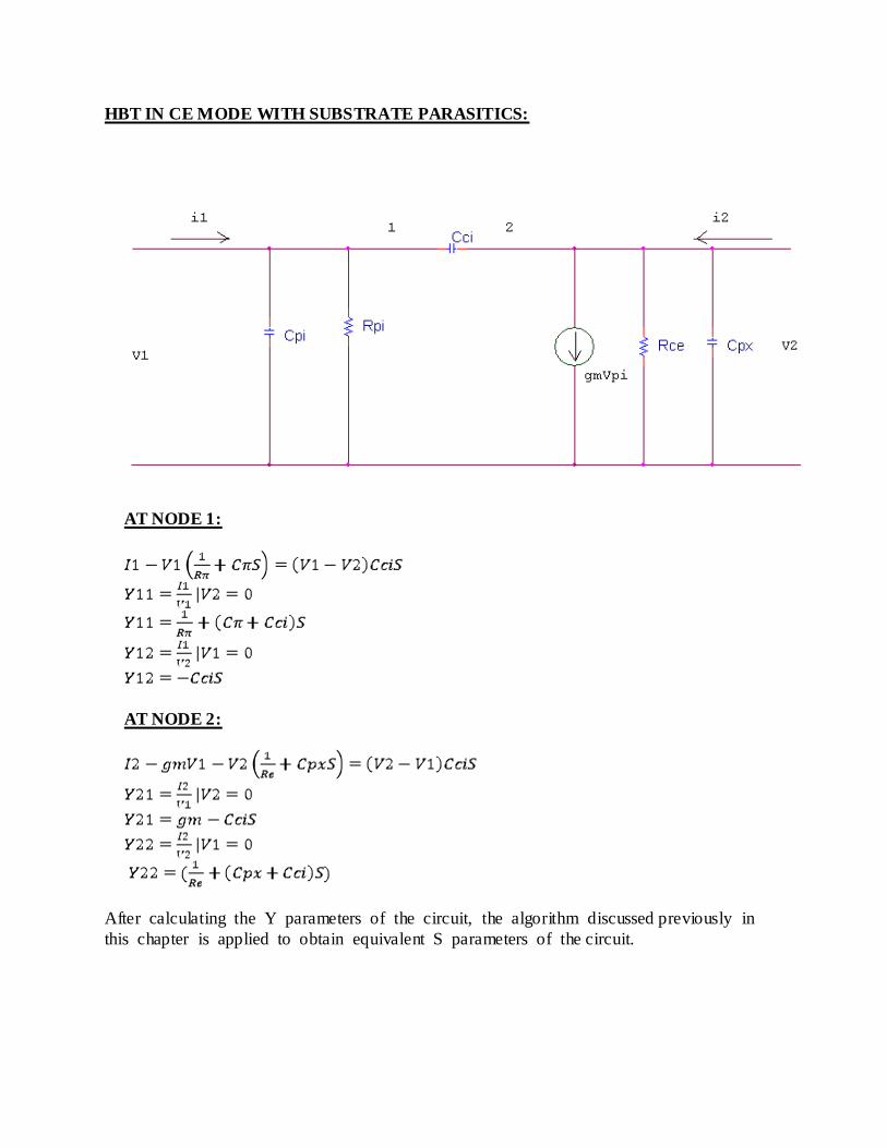
HBT IN CE MODE WITH SUBSTRATE PARASITICS:
AT NODE 1:
AT NODE 2:
After calculating the Y parameters of the circuit, the algorithm discussed previously in
this chapter is applied to obtain equivalent S parameters of the circuit.
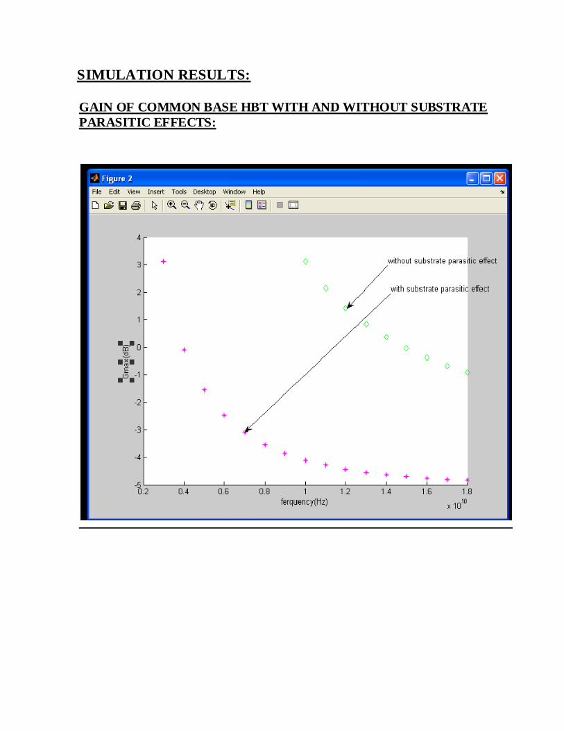
SIMULATION RESULTS:
GAIN OF COMMON BASE HBT WITH AND WITHOUT SUBSTRATE
PARASITIC EFFECTS:
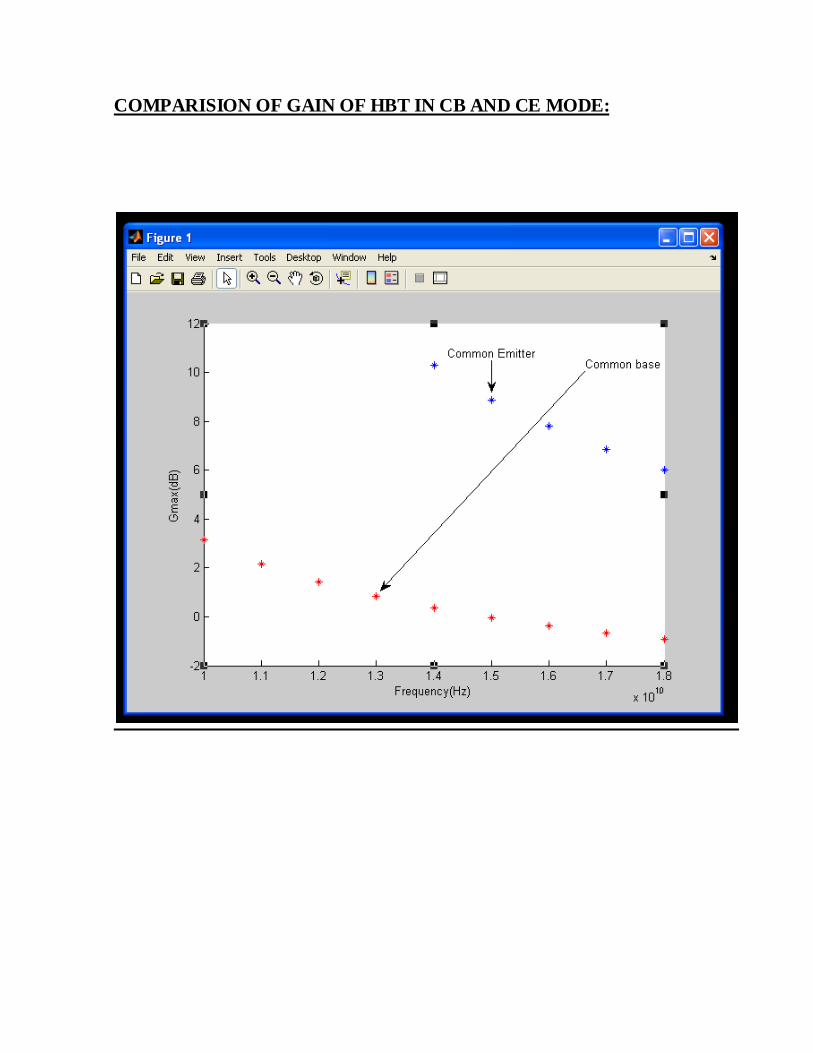
COMPARISION OF GAIN OF HBT IN CB AND CE MODE:

EFFECT OF GROUNDING THE SUBSTRATE OF HBT IN CB MODE :

EFFECT OF GROUNDING THE SUBSTRATE OF HBT IN CE MODE:

CONCLUSION
The graph of transducer power gain and maximum available power gain is drawn
for SiGe HBT with and without taking the substrate parasitic effect. From graph
comparision we found out that both transducer power gain and maximum
available power gain increases with taking into account the substrate parasitic
effect.
From smith chart we can find out forward reflectivity of both input and output port at
any frequency in between 1-18GHz.
If we don’t consider the substrate parasitic effects then the gain of SiGe HBT in CB
mode is much higher than that of in CE mode.
But inclusion of parasitic degrades the superior power gain of HBT in CB mode and
hence its gain reduces than that of in CE mode.
Grounding the substrate is an effective way to reduce the effects of substrate parasitic
on SiGe HBT used as an amplifier.
CHAPTER 3
EFFECTS OF SUBSTRATE PARASITICS
ON SiGe HBT OSCILLATOR

INTRODUCTION
This chapter deals with a possible application of the device for the
designing of microwave oscillators. In this chapter we will design microwave oscillators using
common base and common emitter SiGe HBT. Then we will study the substrate effect on the
operating frequency of both the oscillators.
Design of microwave oscillator using common base SiGe HBT
3.1.Analysis of common base SiGe HBT without considering the substrate effect
The simplified small signal model of common base SiGe HBT ,along with the external
elements of an oscillator is shown in fig.3.1 . Here the external elements are inductive (Lg and
L).
Let V1 and V2 be the voltages at node 1 and 2. Then applying KCL at node 2,
On simplifying,

Fig3.1: Small signal model of common base SiGe HBT without considering the substrate
effect

Fig3.2: Resulting small signal model of common base SiGe HBT after applying Miller’s theorem
After applying Miller’s theorem:
Using Miller’s theorem, the input and output ports of the circuit in Fig. 3.1, may be
represented separately by removing Ro from the circuit and connecting Ro1= and
in parallel to Re and Cu respectively, as shown in F ig.3.2. Here the input port
mainly determines the resonant frequency of the circuit whereas the output port is normally
used for impedance matching .
For oscillations to occur, the imaginary part of to tal impedance of input
port the total admittance of input port must be zero. So from fig.3.2 we can write,

From fig3.2 the Input admittance is given by,
=
=
For oscillation to occur, the imaginary part of the input admittance should be zero, hence
On simplifying the above equation,
---------------------<1>
The frequency at which the above equation becomes zero is called the resonance frequency.
So, we designed an oscillator for a resonance frequency of 16GHz.
In order to satisfy the above condition for f=16GHz, we calculated the value of Lg and L as
L=0.3 and Lg= H

2. Analysis of common base SiGe HBT with considering the substrate effect
The simplified small signal model of common base SiGe HBT ,along with the external
elements of an oscillator is shown in fig.3.3 . Here the external elements are inductive (Lg and
L).
Let V1 and V2 be the voltages at node 1 and 2. Then applying KCL at node 2,
On simplying,
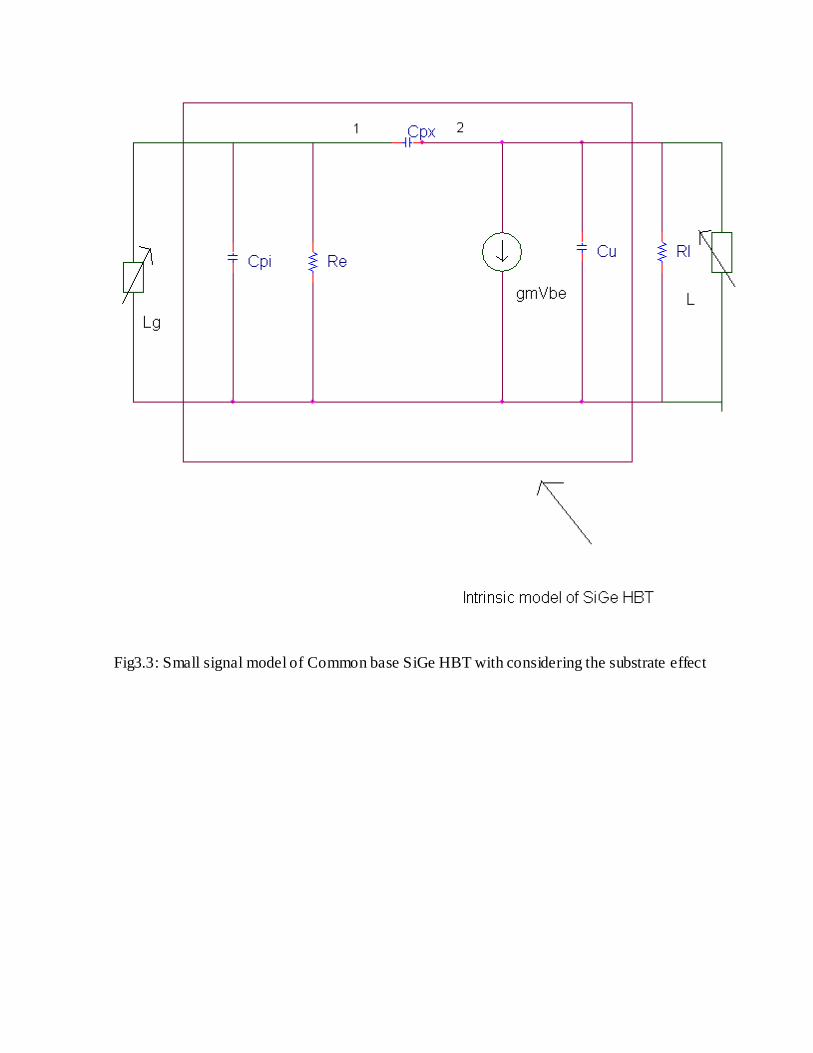
Fig3.3: Small signal model of Common base SiGe HBT with considering the substrate effect

Fig3.4: Resulting small signal model of common base SiGe HBT after applying Miller’s
theorem (with considering the substrate effect)
After applying Miller’s theorem:
Using Miller’s theorem, the input and output ports of the circuit in Fig. 3, may be represented
separately by removing Cpx from the circuit and connecting Cpx1=Cpx(1-k) and
Cpx2=Cpx(1-1/k) in parallel to Re and Cu respectively, as shown in Fig.4. Here the input
port mainly determines the resonant frequency of the circuit whereas the output port is
normally used for impedance matching .
For oscillations to occur, the imaginary part of total impedance of input port i.e. the total
admittance of input port must be zero. So from fig.4 we can write,

But,
Cpx1=Cpx(1-k)
=>
Substituting Cpx1 ,
Input admittance,
=
For oscillation to occur, the imaginary part of the input admittance should be zero, hence we
got
-----------------------------------------<3.2>
For our previously designed oscillator ( ), we calculated the
oscillation frequency (while considering the substrate effect) is reduced to 13.9GHz.

Design of microwave oscillator using common emitter SiGe HBT
3.Analysis of common emitter SiGe HBT without considering the substrate
effect
The simplified small signal model of common emitter SiGe HBT ,along with the
external elements of an oscillator is shown in fig.3.5 . Here the external elements are inductive
(Lg and L).
Let V1 and V2 be the voltages at node 1 and 2. Then applying KCL at node 2,
=>
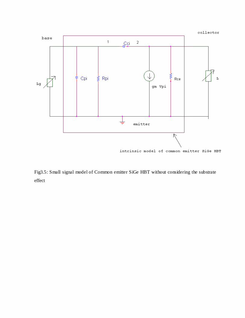
Fig3.5: Small signal model of Common emitter SiGe HBT without considering the substrate
effect
Fig3.6: Resulting small signal model of common emitter SiGe HBT after applying Miller’s
theorem (without considering the substrate effect)
After applying Miller’s theorem:
Using Miller’s theorem, the input and output ports of the circuit in
Fig. 5, may be represented separately by removing Cci from the circuit and connecting
C1=Cci(1-k) and C2=Cci(1-1/k) in parallel to Cpi and Rce respectively, as shown in Fig 3.6.
C1=Cci*(1-k)
=>
For oscillation to occur, the imaginary part of the input admittance should be zero.
Input admittance=

Substituting the value of C1,
Input idmittance=
Imaginary part of the input admittance=0
=>
=>
The frequency at which the above equation becomes zero is called the resonance frequency.
So, we designed an oscillator for a resonance frequency of 10GHz.
In order to satisfy the above condition for f=10GHz, we calculated the value of Lg and L as
L=1.86* H and Lg=8.28* H.
4. Analysis of common emitter SiGe HBT with considering the substrate effect
Here , we will see the substrate effect on the operating frequency
of our designed oscillator. The simplified small signal model of common emitter SiGe HBT
along with the external elements of an oscillator is shown in fig 3.7 .
Let V1 and V2 be the voltages at node 1 and 2. Then applying KCL at
node 2,
=>
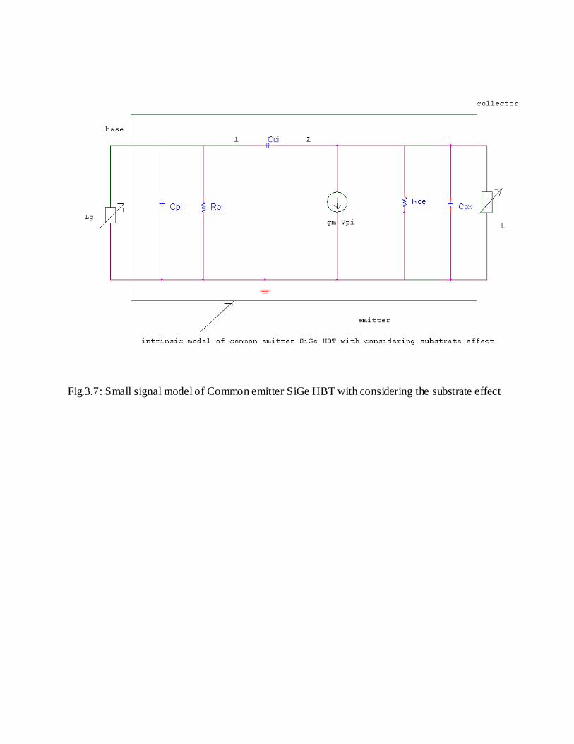
Fig.3.7: Small signal model of Common emitter SiGe HBT with considering the substrate effect

Fig.3.8: Resulting small signal model of common emitter SiGe HBT after applying Miller’s
theorem (considering the substrate effect)
After applying Miller’s theorem:
=>
So, from fig3.8,
the input admittance =
Substituting the value of C1,
Input admittance=

For oscillation to occur, the imaginary part of the input admittance should be zero, so
On simplifying the above equation, we got
For our above designed oscillator (i.e. L=1.86* H and Lg= H)
We calculated the oscillation frequency reduced to Hz.
CONCLUSION:
We have designed a microwave oscillator using common base SiGe Hetero Junction
Bipolar transistor by adding external elements (which are inductive Lg and L) to it.
Here the small signal model of the oscillator is divided into input and output part by using
Miller’s theorem. For oscillation to occur the imaginary part of total impedance of the input
port must be zero. From this condition we got the expression for the oscillation frequency of
the microwave oscillator.
We calculated the value of external elements to be L=0.3nH and Lg=0.5nH,
so that the oscillation occur at 16GHz.
Now taking the substrate effect into account, we found out the expression for the oscillation
frequency of the oscillator, and saw that with substrate effect the oscillation frequency has
been reduced to 13.9GHz.
Then we repeated our experiment for common emitter SiGe hetero junction bipolar
transistor. We designed our microwave oscillator for 10GHz oscillation frequency, by adding
external circuit of L=1.86nH and Lg=8.28nH to it. We saw that, taking the substrate effect
into account, the oscillation frequency has been reduced to 9.187GHz.
Hence, we concluded that the oscillation frequency of the microwave oscillator
decreases due to substrate effect. Again the reduction in oscillation frequency due to substrate
parasitic is more for HBT in CB mode than in CE mode.
REFERRENCES
[1] John D. Cressler “SiGe HBT Technology: A New Contender For Si Based RF And Microwave Circuit Applications” IEEE TRANSACTION ON MICROWAVE THEORY AND
TECHNIQUE S, VOL. 46 , NO. 5, MAY 1998
[2] Hai Huang and Zhenqiang Ma, Pingxi Ma and Marco Racanelli “Influence of Substrate Parasitic Effects on Power Gain Relation between CE and CB SiGe HBTs” -IEEE CONFERENCE PAPER- “Silicon Monolithic Integrated Circuits in RF Systems, 2008. SiRF
2008”,ORLANDO,FL JAN 2008
[3] Damian Costa, William U. Liu, and James S . Harris, Jr. “Direct Extraction of the AlGaAs/GaAs Heterojunction Bipolar Transistor Small- Signal Equivalent Circuit” IEEE TRANSACTIONS ON ELECTRON DEVICES, VOL. 38, NO. 9. SEPTEMBER 1991
[4] Washio, K.; Ohue, E.; Oda, K.; Tanabe, M.; Shimamoto, H.; Onai, T.; Kondo, M. “A selective-epitaxial-growth SiGe-base HBT with SMI electrodes featuring 9.3-ps ECL-gate delay”- IEEE TRANSACTIONS ON ELECTRON DEVICES VOL 16 1999
[5] J.S.Rieh, B.Jagannathan ,D.R.Greenberg, M.Megheli, A.Rylyakov, F.Guarin, Z.Yang,
D.Ahlgren, G.Freeman, P.Cottrell, D.Harame “SiGe heterojunction bipolar transistors and circuits towards terahertz communication applications” IEEE Trans. Microwave Theory and Tech.,VOL. 52, NO. 10, pp 2390-2408,Oct. 2004
[6] Z. Ma and N. Jiang, “On the operation configuration of SiGe HBTs based on power gain
analysis,” IEEE Trans. On Electronic Devices, vol.52,no.2 , pp. 248-255, Feb. 2005.
[7] N. Jiang, Z. Ma, P. Ma and M. Racanelli, “Assesment of influence of interconnect parasitic
on RF performance of muti finger SiGe Power HBTs,” to appear in proceeding of the second european microwave integrated circuits conference (EuMic 07), Munich, Germany, October 8-
12, 2007. [8] P. R. Gray, P. J. Hurst, S. H. Lewis, and R.G.Meyer, Analysis and Design Of Analog
Integrated Circuits, 4th edition NEW YORK:Wiley,2000, pp 183-184


![Paulo MoreiraTransistors1 Outline Introduction – “Is there a limit ?” Transistors – “CMOS building blocks” Parasitics I – “The [un]desirables” Parasitics](https://img.pdfslide.net/doc/110x75/56649d575503460f94a3550a/paulo-moreiratransistors1-outline-introduction-is-there-a-limit-.jpg)