Embed Size (px)
Citation preview

EFFECT OF SURFACE PRETREATMENTS ON THE DEPOSITION OF
POLYCRYSTALLINE DIAMOND ON SILICON NITRIDE SUBSTRATES
USING HOT FILAMENT CHEMICAL VAPOR DEPOSITION METHOD
DAYANGKU NOORFAZIDAH BINTI AWANG SH’RI
UNIVERSITI TEKNOLOGI MALAYSIA
EFFECT OF SURFACE PRETREATMENTS ON THE DEPOSITION OF
POLYCRYSTALLINE DIAMOND ON SILICON NITRIDE SUBSTRATES
USING HOT FILAMENT CHEMICAL VAPOR DEPOSITION METHOD
DAYANGKU NOORFAZIDAH BINTI AWANG SH’RI
UNIVERSITI TEKNOLOGI MALAYSIA
EFFECT OF SURFACE PRETREATMENTS ON THE DEPOSITION OF
POLYCRYSTALLINE DIAMOND ON SILICON NITRIDE SUBSTRATES
USING HOT FILAMENT CHEMICAL VAPOR DEPOSITION METHOD
DAYANGKU NOORFAZIDAH BINTI AWANG SH’RI
A project report submitted in partial fulfilment of the
requirements for the award of the degree of
Master of Engineering (Mechanical-Materials)
Faculty of Mechanical Engineering
Universiti Teknologi Malaysia
MAY 2009

iv
ACKNOWLEDGEMENTS
All praise to Allah s.w.t who taught the mankind what they did not know. My
prayers for my beloved parents, Hj Awang Sh’ri and Hajah Aishah Abdullah who
gave countless sacrifice and did every effort in order to nurture me and provided the
highest moral values.
I am extremely grateful to Professor Dr. Esah Hamzah for her kindly but
rigorous insight gave me the motivation to finish this thesis.
I am also thankful to all technicians in Material and Manufacturing
Laboratory for providing the technical support needed to complete this work. I feel
obliged to express my gratitude towards my course mates for supporting me to
complete this study. I also would like to thanks everyone that contributes directly and
indirectly toward the completion of this study.
Finally, a particular debt of gratitude is due to my beloved late husband,
Allahyarham Heimy Syariffyzal bin Abdul Samat, who helped me at every step of
this work. He always exhibited an extreme degree of love, understanding, sacrifice,
compassion and encouragement for me; otherwise I would never been able to
complete this thesis. His presence in my life will sadly be missed but he will always
be remembered in my prayer.

v
ABSTRACT
The deposition of diamond films on a silicon nitride (Si3N4) substrate is an
attractive technique for industrial applications because of the excellent properties of
diamond. Diamond possesses remarkable physical and mechanical properties such as
chemical resistant, extreme hardness and highly wears resistant. Pretreatment of
substrate is very important prior to diamond deposition to promote nucleation and
adhesion between coating and substrate. Polycrystalline diamonds films have been
deposited on silicon nitride substrate by Hot Filament Chemical Vapor Deposition
(HF-CVD) method. The Si3N4 substrates have been subjected to various pretreatment
methods prior to diamond deposition namely chemical etching and mechanical
abrasion. The structure and morphology of diamond coating have been studied using
X-ray Diffraction (XRD) and Scanning Electron Microscopy (SEM) while diamond
film quality has been characterized using Raman spectroscopy. The adhesion of
diamond films has been determined qualitatively by using Vickers hardness tester. It
was found that the diamond films formed on chemical pretreated substrates has
cauliflower morphology and low adhesive strength but also have low surface
roughness. Substrates that pretreated with sand blasting have yield diamond film
with well-facetted morphology with high crystallinity and better adhesion. However,
the surface roughness of the diamond film deposited on substrates pretreated with
blasting are also higher.
vi
ABSTRAK
Endapan filem intan diatas substrat silikon nitrid (Si3N4) merupakan satu
teknik yang menarik kepada applikasi industri kerana sifat intan yang cemerlang.
Intan memiliki sifat fizikal dan mekanikal yang menakjubkan seperti kalis bahan
kimia, kekerasan yang tinggi dan sangat kalis haus. Pra-penyediaan substrat sebelum
endapan intan adalah sangat penting untuk menggalakkan pertubuhan nuklei dan
meningkatkan rekatan diantara salutan dan substrat. Filem intan polihablur telah
diendapkan diatas substrat silikon nitrid menggunakan kaedah endapan wap kimia
filamen panas. Substrat Si3N4 telah melalui pelbagai kaedah pra-penyediaan sebelum
endapan intan seperti punaran kimia dan lelasan mekanikal. Struktur dan bentuk
salutan intan yang terhasil telah dikaji menggunakan pembelauan sinar X-ray (XRD)
dan mikroskop electron imbasan (SEM) manakala kualiti filem intan telah dikaji
menggunakan spektroskopi Raman. Rekatan filem intan telah dikaji secara kualitatif
menggunakan ujian kekerasan Vickers. Hasil kajian menunjukkan filem intan yang
terbentuk di atas substrate yang melalui pra-penyediaan kimia mempunyai morfologi
cauliflower dan kekuatan rekatan yang rendah tetapi mempunyai kekasaran
permukaan yang rendah. Substrat yang dibagas dengan pasir menghasilkan filem
intan yang mempunyai segi permata dengan kehabluran yang tinggi dan kerekatan
yang lebih bagus. Akan tetapi, kekarasan permukaan filem intan yang diendap diatas
substrat yang dibagas dengan pasir juga lebih tinggi.
vii
TABLE OF CONTENTS
CHAPTER TITLE PAGE
DECLARATION ii
DEDICATION iii
ACKNOWLEDGEMENTS iv
ABSTRACT v
ABSTRAK vi
TABLE OF CONTENTS vii
LIST OF TABLES xi
LIST OF FIGURES xii
LIST OF APPENDICES xvii
1 INTRODUCTION 1
1.1 Background of the research 1
1.2 Problem Statement 2
1.3 Objectives and Scopes of Study 3
1.4 Significance of the Study 4
viii
2 LITERATURE REVIEW - ELECTRONIC PACKAGING 4
2 LITERATURE REVIEW 4
2.1 Introduction 4
2.2 An Overview on Cutting Tools 4
2.2.1 Cutting Tool Materials 5
2.2.1.1 High Speed Steel 5
2.2.1.2 Carbide
2.2.1.3 Alumina based ceramic tools 6
2.2.1.4 Cubic Boron Nitride 7
2.2.1.5 Silicon Nitride based ceramic 7
2.2.2.2 Diamond coatings 8
2.3 Overview of Diamond as Coating Material 8 2.3.1 Structures and properties of diamond 8
2.3.2 Deposition Mechanism of Polycrystalline CVD
diamond
13
2.3.2.1 Nucleation and Growth of CVD diamond 15
2.3.3 Polycrystalline diamond deposition of various
substrates
20
2.3.3.1 Deposition on cemented tungsten carbide 20
2.3.3.2 Deposition on silicon nitride 21
2.3.4 Surface pretreatment 22
2.4 Deposition technique of polycrystalline diamond 25
2.4.1 Introduction 25
2.4.2 Operating principle of CVD 25
2.4.3 CVD diamond deposition techniques 26
2.4.3.2 Arc-Discharge 26
2.4.3.3. Microwave plasma-assisted CVD 27
2.4.3.1 Hot Filament CVD 28
2.5 Conclusion 32
3 RESEARCH METHODOLOGY 33
3.1 Introduction 33
3.2 Sample preparation and Pretreatment 34
3.2.1 Substrates Material 34

ix
3.2.2 Substrate Pretreatments 36
3.2.3 Surface Roughness 39
3.3 Polycrystalline Diamond Deposition by Hot Filament
Chemical Vapor Deposition Technique 40
3.4 Microstructural Characterization 42
3.4.1 Surface Morphology and Thickness by Scanning
Electron Microscopy 42
3.4.2 Surface Topography and Surface Roughness by
Atomic Force Microscopy 43
3.4.3 X Ray Diffraction 43
3.4.4 Diamond Quality and Residual Stress by Raman
Spectroscopy 45
3.5 Adhesion properties by Vickers hardness tester 46
4 RESULTS AND DISCUSSION 48
4.1 Materials 48
4.1.1 Composition and Phase Analysis 48
4.1.2 Hardness Analysis 50
4.2 Pretreatment Analysis 50
4.2.1 Effect of pretreatment on surface roughness and
morphology 50
4.2.1.1 Substrates morphology after pretreatment 50
4.2.1.2 Effect of seeding on diamond nucleation 57
4.3 Effect of chemical etching 61
4.3.1 Introduction 61
4.3.2 Effect of etching time on the morphology of the
diamond film 61
4.3.3 Surface topography and surface roughness by atomic
force microscopy (AFM) 65
4.3.4 Phase analysis using X-ray diffraction 71
4.3.5 Diamond quality analysis using Raman spectra 74
4.4 Effect of Mechanical pretreatment 80
4.4.1 Introduction 80

x
4.4.2 Effect of etching time on the morphology of the
diamond film 80
4.4.3 Surface topography and surface roughness by atomic
force microscopy (AFM) 81
4.4.4 Phase analysis and quality of diamond using X-ray
diffraction 82
4.5 Adhesion analysis of diamond film deposited on various
pretreated substrates. 85
4.5.1 Introduction 85
4.5.2 Adhesion behavior due to different indentation loads85
4.5.3 Determination of adhesive strength 91
4.5.3.1 Adhesive strength determination based on
radial crack 91
4.5.3.2 Adhesive strength determination based on
delamination radius 94
4.5.4 Surface roughness with adhesion 96
4.5.5 Adhesive strength relate with sp2/sp3 ratio 98
5 CONCLUSIONS AND RECOMMENDATIONS 99
5.1 Conclusions 100
5.2 Recommendations for Future Works 100
REFERENCES 101
APPENDICES 107
xi
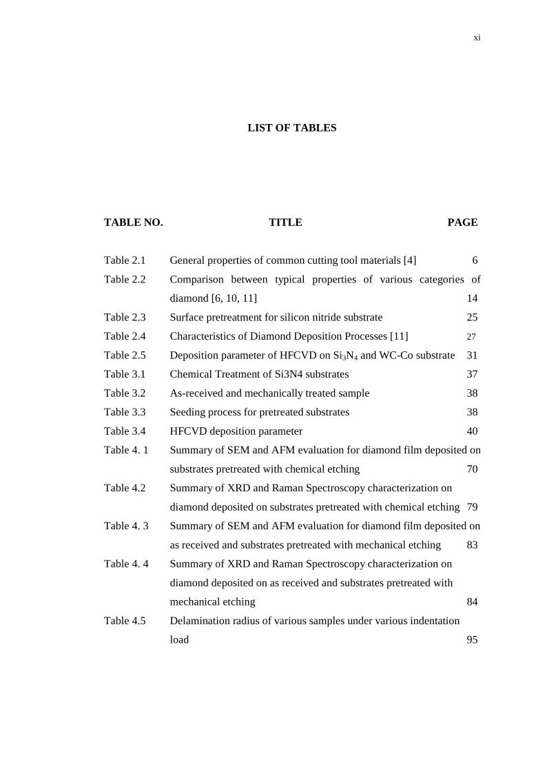
LIST OF TABLES
TABLE NO. TITLE PAGE Table 2.1 General properties of common cutting tool materials [4] 6
Table 2.2 Comparison between typical properties of various categories of
diamond [6, 10, 11] 14
Table 2.3 Surface pretreatment for silicon nitride substrate 25
Table 2.4 Characteristics of Diamond Deposition Processes [11] 27
Table 2.5 Deposition parameter of HFCVD on Si3N4 and WC-Co substrate 31
Table 3.1 Chemical Treatment of Si3N4 substrates 37
Table 3.2 As-received and mechanically treated sample 38
Table 3.3 Seeding process for pretreated substrates 38
Table 3.4 HFCVD deposition parameter 40
Table 4. 1 Summary of SEM and AFM evaluation for diamond film deposited on
substrates pretreated with chemical etching 70
Table 4.2 Summary of XRD and Raman Spectroscopy characterization on
diamond deposited on substrates pretreated with chemical etching 79
Table 4. 3 Summary of SEM and AFM evaluation for diamond film deposited on
as received and substrates pretreated with mechanical etching 83
Table 4. 4 Summary of XRD and Raman Spectroscopy characterization on
diamond deposited on as received and substrates pretreated with
mechanical etching 84
Table 4.5 Delamination radius of various samples under various indentation
load 95

xii
LIST OF FIGURES
FIGURE NO. TITLE PAGE
Figure 2.1 Schematic diagram of crystal structure of hexagonal graphite 11
Figure 2.2: Schematic diagrams of two basic crystal structures of diamond:
hexagonal lonsdaleite and cubic diamond 11
Figure 2.3 Schematic of unit cell of cubic diamond 12
Figure 2.4: Schematic of the simple crystals shape of diamonds 13
Figure 2.5 Idiomorphic crystal shapes of diamond for different values of the
growth parameter, α. 13
Figure 2.6 Generalized schematic of the physical and chemical process occurring
in CVD diamond reactor 16
Figure 2.7 Simplified form of the Bachmann triangle C-H-O composition
diagram in which below CO tie-line, no film growth will occur.
Above the CO tie-line, non-diamond carbon is deposited except in a
narrow window close to the tie-line which produces polycrystalline
diamond films 17
Figure 2.8 Free energy diagram of three dimensional crystal formation (∆G3D)
at constant supersturation (∆µ) as a function of the number of its
particle, n. [13] 18
Figure 2.9: Schematic of the reaction process occurring at the diamond surface
leading to stepwise addition of CH3 species and diamond growth 20
Figure 2.10 Growth process of a diamond film on a non-diamond substrates: (a)
nucleation of individual crystallites (b-c) termination of nucleation,
and growth of indicidual crystallite (d) faceting and coalescence of
individual crystallites and formation of continuous film (e-f) some

xiii
crystals grow faster and swallow their neighbours during growth of
continuous film [6]. 21
Figure 2.11 Schematic of arc-discharge apparatus for the deposition of diamond28
Figure 2.12 Schematic of microwave-plasma deposition 29
Figure 2.13 Hot Filament Apparatus for deposition of diamond 30
Figure 2.14 Schematic diagram showing the mechanisms of diamond nucleation
enhancement on biases substrate. (a) Negative biasing: carbon
containing cations are accelerated toward the substrate surface. (b)
Positive biasing: electrons are accelerated toward the substrate surface
and bombard carbon-containing molecules adsorbed on the surfaces
[6]. 32
Figure 3.1 Experimental Flow Chart 35
Figure 3.2 Ultrasonic cleaner used to clean the sample 36
Figure 3.3 Schematic of a profilometer used to determine the surface roughness
of the materials 39
Figure 3.4 Hot filament chemical vapor deposition (a) actual equipment and (b)
schematic drawing of HFCVD equipment. 41
Figure 3.5 HFCVD chamber configuration showing (a) front view and (b) side
view. 41
Figure 3.6 Scanning Electron Microscopy used to investigate the morphology of
deposited polycrystalline diamond 42
Figure 3.7 Atomic Force Microscopy used for topography and surface roughness
analysis 43
Figure 3.8 Bragg’s Law explaining the diffraction of crystals 44
Figure 3.9 X-Ray Diffractometer (XRD) used to determine composition and
phase analysis of the coating 44
Figure 3.10 Raman Spectroscopy Equipment 46
Figure 3.11 Vickers Hardness Tester indenter (a) actual equipment and (b)
schematic of hardness measurement 47
Figure 4.1 (a) As-received Si3N4 substrates and (b) optical micrograph of Si3N4
(x200) 48
Figure 4.2 EDX spectrum of Si3N4 49
Figure 4.3 XRD spectrum of as-received Si3N4 49
Figure 4.4 Vickers indentation on Si3N4 50
xiv
Figure 4.5 FE-SEM micrograph of substrates surface due to (a) acid etching, (b)
strong acid etching and (c) basic etching. 52
Figure 4.6 AFM image analysis showing (a) top view and (b) 3-dimensional
view of substrates undergoes strong acid etching for 20 minutes. 52
Figure 4.7 Mechanism of wet chemical etching 53
Figure 4.8 AFM images of surface topography of Si3N4 substrate pretreated by
sand blasting. 54
Figure 4.9 Schematic diagram of blasting mechanism 55
Figure 4.10 AFM images of surface topography of Si3N4 substrate pretreated by
grinding process 55
Figure 4.11 Schematic diagram of grinding mechanism 56
Figure 4.12 Surface roughness (Ra) before and after surface pretreatment 57
Figure 4.13 Diamond nucleation on substrates pretreated with (a) acid etching (b)
strong acid etching and (c) basic etching 58
Figure 4.14 Diamond nucleation on non-seeded, (a) as-received (b) pretreated by
blasting and (c) pretreated by grinding substrates. 59
Figure 4. 15 Schematic diagram of mechanisms for diamond nucleation
enhancement of scratched substrates [7] 60
Figure 4.16 SEM micrograph of Vickers indentation on Si3N4 substrates
pretreated by grinding on (a) seeded and (b) unseeded sample. 60
Figure 4.17 SEM showing diamond film deposited on substrate pretreated with
acid etching for (a) 10 (b) 20 and (c) 30 minutes. 62
Figure 4.18 SEM showing diamond film deposited on substrate pretreated with
strong acid etching for (a) 10 (b) 20 and (c) 30 minutes. 63
Figure 4.19 SEM showing diamond film deposited on substrate pretreated with
basic etching for (a) 10 (b) 20 and (c) 30 minutes. 63
Figure 4.20 Schematic of ballas-like particle growth suggesting preferential <110>
orientation during NCD film deposition [10]. 64
Figure 4.21 AFM 3D topography of diamond film deposited on acid etched
substrates for (a) 10 (b) 20 and (c) 30 minutes. 65
Figure 4.22 AFM 3D topography of diamond film deposited on strong acid etched
substrates for (a) 10 (b) 20 and (c) 30 minutes. 66
Figure 4. 23 AFM 3D topography of diamond film deposited on basic etched
substrates for (a) 10 (b) 20 and (c) 30 minutes. 67
xv
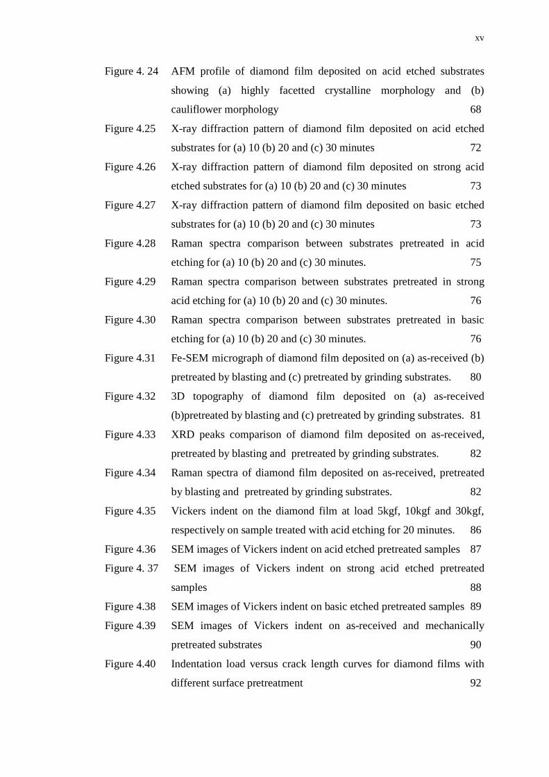
Figure 4. 24 AFM profile of diamond film deposited on acid etched substrates
showing (a) highly facetted crystalline morphology and (b)
cauliflower morphology 68
Figure 4.25 X-ray diffraction pattern of diamond film deposited on acid etched
substrates for (a) 10 (b) 20 and (c) 30 minutes 72
Figure 4.26 X-ray diffraction pattern of diamond film deposited on strong acid
etched substrates for (a) 10 (b) 20 and (c) 30 minutes 73
Figure 4.27 X-ray diffraction pattern of diamond film deposited on basic etched
substrates for (a) 10 (b) 20 and (c) 30 minutes 73
Figure 4.28 Raman spectra comparison between substrates pretreated in acid
etching for (a) 10 (b) 20 and (c) 30 minutes. 75
Figure 4.29 Raman spectra comparison between substrates pretreated in strong
acid etching for (a) 10 (b) 20 and (c) 30 minutes. 76
Figure 4.30 Raman spectra comparison between substrates pretreated in basic
etching for (a) 10 (b) 20 and (c) 30 minutes. 76
Figure 4.31 Fe-SEM micrograph of diamond film deposited on (a) as-received (b)
pretreated by blasting and (c) pretreated by grinding substrates. 80
Figure 4.32 3D topography of diamond film deposited on (a) as-received
(b)pretreated by blasting and (c) pretreated by grinding substrates. 81
Figure 4.33 XRD peaks comparison of diamond film deposited on as-received,
pretreated by blasting and pretreated by grinding substrates. 82
Figure 4.34 Raman spectra of diamond film deposited on as-received, pretreated
by blasting and pretreated by grinding substrates. 82
Figure 4.35 Vickers indent on the diamond film at load 5kgf, 10kgf and 30kgf,
respectively on sample treated with acid etching for 20 minutes. 86
Figure 4.36 SEM images of Vickers indent on acid etched pretreated samples 87
Figure 4. 37 SEM images of Vickers indent on strong acid etched pretreated
samples 88
Figure 4.38 SEM images of Vickers indent on basic etched pretreated samples 89
Figure 4.39 SEM images of Vickers indent on as-received and mechanically
pretreated substrates 90
Figure 4.40 Indentation load versus crack length curves for diamond films with
different surface pretreatment 92

xvi
Figure 4.41 Adhesive strength of diamond film deposited on various surface
pretreated substrates 92
Figure 4.42 Crack response of diamond deposited on (a) basic etched and (b)
pretreatment by blasting to Vickers indentation 93
Figure 4.43 Typical crack response of diamond film due to Vickers indentation
observed under optical microscopy. 94
Figure 4.44 Plot of delamination radius versus load for strong acid pretreated
substrates 95
Figure 4.45 Adhesive strength of diamond films. 96
Figure 4.46 Relationship between surface roughness of diamond film and
adhesive strength 97
Figure 4.47 Relationship between adhesion strength and sp2/sp3 ratio of diamond
film 98

xvii
LIST OF APPENDICES
APPENDIX TITLE PAGE
A1 Abstract accepted for International Conference on Advances in
Mechanical Engineering 2009-(ICAME 2009), 24-25 June 2009 ,
Shah Alam, Malaysia. 108
A2 Abstract accepted for Advances in Materials and Processing
Technologies (AMPT) 2009 (AMPT 2009), 26 - 29 October 2009,
Kuala Lumpur, Malaysia. 109

CHAPTER 1
INTRODUCTION
1.1 Background of the research
Apart from their appeal as highly treasured gemstones, diamond possesses a
remarkable physical properties such as extreme hardness, high thermal conductivities,
excellent infrared transparency and remarkable semiconductor properties making
diamond one of technologically valuable materials. However, it has proved very difficult
to exploit these properties, due to the cost and scarcity of large natural diamond.
Many attempts have been made to synthesize diamond artificially using graphite
as starting material. This proved very difficult, mainly because at room temperature and
atmospheric pressure, graphite is the thermodynamically stable allotrope of carbon.
Although the standard enthalpies of diamond and graphite are differ only by 2.9 kJ mol-
1, a large activation barrier separates the two phases preventing interconversion between
them at room temperature [1]. To overcome these problem, high pressure high
temperature (HPHT) growth techniques has been introduced by General Electric to
produce industrial diamond. However, the drawback of HPHT method is that it still

2
produces diamond in form of single crystal thus limiting the range of application it can
be used.
This leads to the idea of producing diamond from gas phase at much lower
pressure in which carbon atoms could be added one-at-a-time to an initial template, in
such a way tetrahedrally bonded carbon network forms. It can be achieved by using
chemical vapor deposition (CVD) method. CVD involves a gas phase chemical reaction
occurring above solid surfaces, which causes deposition onto that surface. All CVD
techniques for producing diamond film require a mean of activating gas-phase carbon-
containing precursor molecules[2]. This gas phase activation is achieved typically by
using one of these three basic methods:
• External heating (as in hot filament CVD)
• Plasma activation (as in Plasma assisted CVD)
• A combination of thermal and chemical activation (as in flame CVD)
The applications for which CVD diamond films can be used are closely related to
the various extreme physical properties they exhibit. The extreme hardness and high
wear resistance of the diamond makes it an ideal candidate for use as coating material in
cutting tool.
1.2 Problem Statement
Diamond coating have a great application as wear resistant layers on tools. Such
diamond-coated hard metal and ceramic inserts are used successfully in machining fiber-
reinforced plastic, graphites and aluminium alloys. However, in order for CVD diamond
to be used as coating for tools and wear parts, it has been shown that two problem must
3
be overcome first The problems are the diffusion of atoms from the substrate to the
diamond and diffusion of carbon atoms to the substrate, and also the adhesion and
residual stress in interlayer of diamond coating [3]. Poor adhesion can be caused by
many factors such as mismatch of coefficient of thermal expansion (CTE) between
diamond and substrate, residual stress, impurities and others.
1.3 Objectives and Scopes of Study
The objectives of this study are to study the effect of substrate surface treatment
on morphology, coating adhesion, surface roughness and residual stress of
polycrystalline diamond coated on silicon nitride. Surface treatment of the substrate is
very important in order to produce high quality diamond coating with high adhesion
strength.
The scope of the research includes:
a) Polycrystalline diamond deposited on silicon nitride substrate using Hot Filament
Chemical Vapor Deposition machine using 99% CH4 gas as precursor.
b) Prior to diamond deposition, the substrate undergoes various surface
pretreatment processes as following:
i. The surface was blasted with SiC 180 for 30 sec (mechanical
pretreatment)
ii. The surface was grinded with 180 grit for 5 minutes followed by 600 grit
for 5 minutes (mechanical pretreatment)
iii. The surface was etched with various chemical reagents (chemical
etchings)

4
c) Characterization on microstructure, morphologies and mechanical properties
using scanning electron microscopy, atomic force microscopy, Raman Spectroscopy, X-
ray diffraction and Vickers hardness indenter
1.4 Significance of the Study
In an effort to enhance diamond nucleation and to control film growth
morphology, the effect of surface conditions on nucleation processes will be investigated
to select the optimum surface pretreatment method. The chemical properties and surface
conditions of substrate materials critically influence surface nucleation processes of
diamond in CVD. Thus, based on the output of this study, optimum surface treatment
technique and deposition parameter will be determined to produce goof quality
polycrystalline diamond coating.