Embed Size (px)
Citation preview

materials
Article
Effect of WEDM Process Parameters on SurfaceMorphology of Nitinol Shape Memory Alloy
Rakesh Chaudhari 1 , Jay J. Vora 1 , Vivek Patel 2,3 , L. N. López de Lacalle 4,* andD. M. Parikh 1
1 Department of Mechanical Engineering, School of Technology, Pandit Deendayal Petroleum University,Raisan, Gandhinagar 382007, India; [email protected] (R.C.); [email protected] (J.J.V.);[email protected] (D.M.P.)
2 School of Material Science and Engineering, Northwestern Polytechnical University, Shaanxi 710072, China;[email protected]
3 Department of Engineering Science, Division of Welding Technology, University West,46186 Trollhättan, Sweden
4 Department of Mechanical Engineering, University of the Basque Country,Escuela Superior de Ingenieros Alameda de Urquijo s/n., 48013 Bilbao, Spain
* Correspondence: [email protected]
Received: 30 September 2020; Accepted: 31 October 2020; Published: 3 November 2020�����������������
Abstract: Nickel–titanium shape memory alloys (SMAs) have started becoming popular owing totheir unique ability to memorize or regain their original shape from the plastically deformed conditionby means of heating or magnetic or mechanical loading. Nickel–titanium alloys, commonly knownas nitinol, have been widely used in actuators, microelectromechanical system (MEMS) devices,and many other applications, including in the biomedical, aerospace, and automotive fields. However,nitinol is a difficult-to-cut material because of its versatile specific properties such as the shapememory effect, superelasticity, high specific strength, high wear and corrosion resistance, and severestrain hardening. There are several challenges faced when machining nitinol SMA with conventionalmachining techniques. Noncontact operation of the wire electrical discharge machining (WEDM)process between the tool (wire) and workpiece significantly eliminates the problems of conventionalmachining processes. The WEDM process consists of multiple input parameters that should becontrolled to obtain great surface quality. In this study, the effect of WEDM process parameters onthe surface morphology of nitinol SMA was studied using 3D surface analysis, scanning electronmicroscopy (SEM), and energy-dispersive X-ray (EDX) analysis. 3D surface analysis results indicateda higher value of surface roughness (SR) on the top of the work surface and a lower SR on the bottomportion of the work surface. The surface morphology of the machined sample obtained at optimizedparameters showed a reduction in microcracks, micropores, and globules in comparison with themachined surface obtained at a high discharge energy level. EDX analysis indicated a machinedsurface free of molybdenum (tool electrode).
Keywords: shape memory alloy; nitinol; WEDM; shape memory effect; surface morphology;molybdenum tool wire
1. Introduction
In the present scenario of manufacturing competitiveness, the adoption of new technologiesis essential to overcome the challenges of achieving component accuracy, high quality, acceptablesurface finish, increased production rate, enhanced product life, and reduced environmental impact.Beyond these conventional challenges, the machining of newly developed smart materials also requires
Materials 2020, 13, 4943; doi:10.3390/ma13214943 www.mdpi.com/journal/materials

Materials 2020, 13, 4943 2 of 14
inputs of intelligent machining strategies. For the manufacturing processes, the accuracy of the finishedproduct is mainly dependent on its input process parameters. Therefore, it is necessary to control theinput parameters and secure their optimum values. One such newly developed generation of alloysis the shape memory alloys (SMAs). SMAs display an exceptional characteristic of regaining theirshape when they are heated. Nickel–titanium alloy is one of the shape memory alloys, which is knownas nitinol in respect of its innovation at the Naval Ordnance Laboratory (NOL) [1]. Shape memoryalloys were initially revealed by Swedish physicist Arne Olander [2]. He found that Au–Cd alloysreturned to their initial shape and size after heating above a certain temperature even after their plasticdeformation in the cold state. Out of numbers of combinations of SMAs, nitinol became a famousshape memory alloy owing to low production cost as compared to other SMAs, safer and easierhandling, and superior mechanical properties. Nitinol SMAs have been applied in various areas likeair conditioning vents, electronic cable connectors, and valves [3]. Over the last decade, the areas ofapplication also spread to aerospace, oil industries, automobiles, and robotics. These smart materialspossess the main characteristics of superelasticity (SE) and shape memory effect (SME) [1]. Nitinol isconsidered an ideal material in the biomedical field owing to its properties like biocompatibility andwear and corrosion resistance [4,5]. Due to the functional properties of nitinol SMAs, their biomedicalapplication has proven successful by increasing the possibility as well as the performance quality ofminimally invasive surgeries. The nickel–titanium SMA is highly biocompatible, which makes it usefulin orthopedic implants, surgical instruments, cardiovascular devices, and orthodontic devices [6,7].Nitinol SMA is categorized into two different types, namely shape memory and superelastic. If thetemperature of shape recovery is less than the room temperature, it is recognized as superelastic;if the temperature of the shape recovery is greater than room temperature, it is recognized as shapememory [8]. There are several challenges faced when using conventional machining techniques tomachine nitinol SMA; these challenges are due to severe strain hardening, high ductility, poor chipbreaking, superelasticity, burr formation, and high wear and corrosion resistance [9,10]. Weinert andPetzoldt concluded that the machining of NiTi-based alloys is complex using conventional techniqueslike turning, drilling, and deep hole drilling. Poor chip breaking, tool wear, and burr formation havebeen observed while machining shape memory alloys using conventional machining techniques
Wire electrical discharge machining (WEDM) is a type of nonconventional machining methodwhich is more preferable to overcome these defects [10]. The WEDM process is applicable to allconductive materials regardless of material hardness [11–14]. The WEDM process creates a series ofsparks that helps to remove the material from the work surface. These sparks are generated betweenthe wire (electrode) and the workpiece in the presence of a dielectric fluid. The WEDM process consistsof a high number of process parameters that should be controlled to acquire great surface quality andcontrol the resulting metallurgical and mechanical properties. Achieving superior performance ofnitinol using the WEDM process requires the optimized parameter settings of input process parameterssuch as discharge current (I), pulse-off time (Ton), pulse-on time (Toff), and dielectric fluid pressurefor machining of nitinol SMA [15]. Chaudhari et al. [10] identified current (I), Ton, and Toff as keyinput parameters for machining of superelastic SMA. Their results indicated that all the parameters aresignificant for achieving simultaneous output parameters. In another study, Majumder and Maity [16]used the WEDM technique for the simultaneous optimization of multiple input parameters of nitinolSMA. Soni et al. [17] identified the appropriate level of pulse-on time and servo voltage for the reductionof microcracks. Proper selection of input process parameters is a key factor in the WEDM process toavoid wire rupture problems and the formation of larger craters on the work surface [18]. In pastresearch, electrodes of brass and copper wires have been used for surface analysis of SMAs for samplesmachined by WEDM [19,20].
Recently, we conducted a Pareto analysis of WEDM input parameters for machining of nitinolSMA using the heat transfer search (HTS) algorithm [21]. The HTS algorithm was found to be effectivefor predicting and optimizing the input values for all objective functions. ANOVA test results showedthe robustness of the generated empirical models for the optimization of multiple responses. The key

Materials 2020, 13, 4943 3 of 14
focus of the present study is on the influence of input parameters on the surface integrity of themachined surface. Based on reviewed literature and machining capabilities, current (I), pulse-off
time (Toff), and pulse-on time (Ton) were selected as three key input parameters surface roughness(SR), material removal rate (MRR), and microhardness (MH) were selected as output characteristics.For surface morphology, sets of parameters with high and low discharge energy levels and a setof optimized process parameters were considered. In past studies, more focus was placed on theparametric optimization of nitinol alloys. However, not much has been reported on surface integrityafter conducting parametric optimization. In the present study, scanning electron microscope (SEM)and energy-dispersive X-ray analysis (EDX) were used to study elemental composition, surface analysis,and phase analysis after the machining of nitinol SMA. The aim of the present study was to providesignificant input to end-users for the selection of WEDM process parameters for nitinol SMA.
2. Materials and Methods
In the current study, a Concord WEDM machine DK7732 with EDM oil (Concord Limited,Bangalore, India) as dielectric fluid was used to machine the samples of nitinol SMA (Procured fromSMA Wires, Ahmedabad, India). The chemical composition of nitinol SMA (Ni55.8Ti) used in thepresent study is shown in Table 1. A nitinol bar with a diameter of 6 mm was utilized to machinetests for surface investigation. In a past report, the impact of input parameters was inspected bycutting sample sizes of 1.5 mm. A similar size of 1.5 mm was favored in the current examination.A reusable molybdenum wire (Concord Limited, Bangalore, India) of 0.18 mm diameter was used as atool electrode.
Table 1. Chemical composition of nitinol shape memory alloy (SMA).
Element Ti Ni Co Cu Cr Fe Nb C H O N
Wt (%) Balance 55.78 0.005 0.005 0.005 0.012 0.005 0.039 0.001 0.034 0.001
The heat transfer search (HTS) technique has been used for multiobjective optimization of multiplevariables like MRR, SR, and MH [10,21]. The HTS algorithm functions on basis of the transfer of heatowing to the interface between the system particles and the surroundings to achieve thermal stability.Thermal stability in the transfer of heat between system and surroundings can be obtained from athermodynamically imbalanced system. To reach thermal stability, three heat transfer phenomena,namely conduction, convection, and radiation, contribute to a large extent. As such, the three phasesof conduction, convection, and radiation are considered during the implementation of the HTSalgorithm. During the implementation of the HTS algorithm, each heat transfer phenomenon has thesame opportunity for heat transfer, and each generation decides any one of these three phenomenarandomly. Arbitrarily created population commences the HTS algorithm, in which the system consistsof ‘n’ number of particles (population size) and temperature level (input variables). Subsequently,arbitrarily chosen heat transfer phenomena update the population size for each generation. In the nextstage, an updated solution having a good functional rate gets accepted and the worst solution getsreplaced by elite solutions [10]. The flow chart of the HTS algorithm is shown in Figure 1.

Materials 2020, 13, 4943 4 of 14
Figure 1. Flow chart of the heat transfer search (HTS) algorithm.
2.1. Conduction Phase
Equations (1) and (2) are used to update the solutions for the conduction phase:
X′j,i =
Xk,i +(−R2Xk,i
), iff
(Xj
)> f(Xk)
Xj,i +(−R2Xj,i
), iff
(Xj
)< f(Xk)
; ifg ≤ gmax/CDF (1)
X′j,i =
Xk,i + (−riXk,i), iff(Xj
)> f(Xk)
Xj,i +(−riXj,i
), iff
(Xj
)< f(Xk)
; ifg > gmax/CDF (2)
where X′j,i is the updated solution; j = 1, 2, . . . , n; k is a randomly selected solution; j , k; k ∈ (1, 2, . . . , n);i is a randomly selected design variable; i ∈ (1, 2, . . . , m); gmax is the maximum number of generationspecified; CDF is the conduction factor; R is the probability variable; R ∈ {0, 0.3333}; and ri ∈ {0, 1} is auniformly distributed random number [10].
2.2. Convection Phase
Equations (3) and (4) are used to update the solutions for convection phase:
X′j,i = Xj,i + R× (Xs −Xms × TCF) (3)
TCF =
{abs(R− ri), ifg ≤ gmax/COF
round(1 + ri), ifg > gmax/COF(4)

Materials 2020, 13, 4943 5 of 14
where X′j,i is the updated solution; j = 1, 2, . . . , n; i = 1, 2, . . . , m; COF is the convection factor; R is theprobability variable; R ∈ {0.6666, 1}; ri ∈ {0, 1} is a uniformly distributed random number; Xs is thetemperature of the surroundings; Xms is the mean temperature of the system; and TCF is a temperaturechange factor [10].
2.3. Radiation Phase
Equations (5) and (6) are used to update the solutions for radiation phase:
X′j,i =
Xj,i + R×(Xk,i −Xj,i
), iff
(Xj
)> f(Xk)
Xj,i + R×(Xj,i −Xk,i
), iff
(Xj
)< f(Xk)
; ifg ≤ gmax/RDF (5)
X′j,i =
Xj,i + ri ×(Xk,i −Xj,i
), iff
(Xj
)> f(Xk)
Xj,i + ri ×(Xj,i −Xk,i
), iff
(Xj
)< f(Xk)
; ifg > gmax/RDF (6)
where X′j,i is the updated solution; j = 1, 2, . . . , n; i = 1, 2, . . . , m; j, k; k ∈ (1, 2, . . . , n), and k is a randomlyselected molecule; RDF is the radiation factor; R is the probability variable; R ∈ {0.3333, 0.6666};and ri ∈ {0, 1} is a uniformly distributed random number [10].
It is not possible to cover the entire machining range in the design of the experiment. Based onthe literature, suitable ranges for input process parameters were considered while conducting theexperiments as follows:
• Pulse on time: 35 µs ≤ Ton ≤ 55 µs;• Pulse off time: 10 µs ≤ Toff ≤ 20 µs;• Current: 2 A ≤ I ≤ 4 A.
However, there is a possibility that the optimized parameter settings may be outside theseconsidered ranges. For this, the machining range was considered between the extreme limits of inputprocess parameters while implementing the HTS algorithm as follows:
• Pulse on time: 1 µs ≤ Ton ≤ 110 µs;• Pulse off time: 1 µs ≤ Toff ≤ 32 µs;• Current: 1 A ≤ I ≤ 6 A.
The optimum values for selected responses were found at Ton of 40 µs, Toff of 12 µs, and currentof 1 A [21]. For these optimal conditions, the responses of other output variables were predicted,and a validation test was performed using these predicted process parameters. The HTS algorithmwas found to be capable of successfully predicting and optimizing the process parameters as thedifference between the predicted and measured value was negligible. In the present study, the effectof input process parameters at these optimum levels was studied in detail on the surface integrity ofthe machined surface. Figure 2 shows the slide-flushing mechanism (from above) used in the currentstudy during the WEDM process. To understand the variation of SR in different areas of the machinedsurface, a three-dimensional (3D) digital microscope with a noncontact-type probe (Keyence VHX-600,China) was used. Keyence VHX-600 digital microscope (Keyence VHX-600, China) was used to recordthe variation of SR values. The recorded SR values in the current study have an arithmetic averageroughness (Ra) in µm. The surface morphology of the machined samples was examined using SEM andEDX equipment from Tescan (Vega Tescan, India). Etchant (82 mL H2O + 14 mL HNO3 + 4 mL HF)was used for nitinol SMA.

Materials 2020, 13, 4943 6 of 14
Figure 2. Flushing mechanism for the wire electrical discharge machining (WEDM) process.
3. Results and Discussion
3.1. Analysis of SR Using 3D Digital Microscope
The sample machined using the optimized set of parameters (Ton of 40 µs, Toff of 12 µs, and currentof 1 A) was subjected to 3D analysis. Differential scanning calorimetry (DSC) (Netzsch, Selb, Germany)testing revealed that the WEDM sample machined using the optimized set of parameters had retention ofshape memory effect when compared to that of the starting base material [21]. Figure 3 shows the topsurface of the machined sample, with SR values indicated at various locations. The top surface of themachined sample shows the highest value of SR, which is indicated by green color; the bottom surface ofthe machined sample shows the lowest value of SR, as indicated by blue color. While red color indicatesthe highest SR in the image, these points were not taken into account as they are outside of the machinedsurface. As indicated by the wire travel direction shown in Figure 3, SR was measured on the surface fromleft to right. Figure 4 shows the machined surface of superelastic nitinol SMA, with SR values represented.It can be clearly observed that the average value of SR in the current study (Figure 3) is less than theaverage value of SR obtained for superelastic nitinol shape memory alloy (Figure 4) [22].
Figure 3. Surface machined under optimized process parameters.

Materials 2020, 13, 4943 7 of 14
Figure 4. Machined surface representing surface roughness (SR) values for superelastic nitinol [22].
The dielectric flushing mechanism from above was the main reason for obtaining a higher valueof SR on the top surface of the sample; i.e., a greater area of the top surface is exposed to the dielectricfluid. This in turn increases the discharge energy, which results in a greater amount of debris removal.It also increases the material removal rate due to the higher value of discharge energy. However,at the bottom surface of the sample, the supply of dielectric fluid is lower, which minimizes thedischarge energy and SR of the bottom region. An increase in dielectric fluid pressure increases thedischarge energy which increases the SR and forms the larger craters on the surface of the workpiece [23].Figures 5 and 6 support this conclusion of differences in SR between different locations of the worksurface. Figures 5 and 6 represent the detailed SR analysis of the machined sample at the outermostand innermost peripheries, respectively. The number of data points for each periphery is differentdue to different circumferential lengths for both peripheries. A distance of 0.43 mm was taken intoaccount between the two consecutive SR measurements. The outermost periphery has a circumferentiallength of 20,920 µm with 48,651 data points, whereas the innermost periphery has a circumferentiallength of 8345 µm with 19,406 data points. The lowest value of SR was obtained at the bottom surface.while the maximum SR was observed to be at the top surface. However, it is recommended to haveidentical flushing pressure coming from both directions (above and below) of the workpiece to avoidany variation in SR value on the machined surface. This might result in giving a higher average SRvalue for the machined surface.
Wire rupture occurs with an increase in crater size. To avoid this problem, discharge energy mustbe at an optimum level. A lower SR value can be achieved at a lower discharge energy level. Loweringthe values of pulse-on time and current results in a lower discharge energy level [24]. However, a lowervalue of pulse-off time gives a higher discharge energy level as it minimizes the time between twoconsecutive sparks. Pursuant to the same, lower discharge energy can be obtained at lower values ofpulse-on time and current and a higher value of pulse-off time. The machined sample considered inthe current study was obtained at optimized parameter settings (Ton of 40 µs, Toff of 12 µs, and currentof 1 A). These values show that discharge energy was not at a lower or higher level as these values arederived for multiple response variables such as MRR, SR, and MH. Table 2 shows the higher dischargeenergy level of an optimized set of parameters in our previously reported study of the surface analysisof superelastic SMA in comparison with the current study [22]. Lower discharge energy at optimizedparameter settings in the current study gives lower SR values as compared to the previously reportedstudy, without compromising the optimum values of other response variables such as MRR and MH.The average value of SR in the current study is less than the average value obtained for superelastic

Materials 2020, 13, 4943 8 of 14
nitinol shape memory alloy [22]. This is because of the lower discharge energy for parametric settingsof nitinol SMA as compared to the discharge energy of superelastic nitinol shape memory alloy.
Figure 5. Surface analysis of machined sample at outermost periphery.
Figure 6. Surface analysis of machined sample at innermost periphery.

Materials 2020, 13, 4943 9 of 14
Table 2. 3D surface analysis comparison of present study with past study [22].
Researcher Work Material
InputParameters at
HighDischarge
Energy Level
InputParameters at
Low DischargeEnergy Level
InputParameters at
OptimizedParameters
Settings
Remarks
Chaudhari et al.[22]
SuperelasticNitinol SMA
Ton = 110 µs,Toff = 32 µs,
Current = 6 ANot reported
Ton = 65 µs,Toff = 32 µs,
Current = 6 A
3D surface analysis shows highervalue of SR (1 to 148 µm) on
machined surface at optimizedparameter settings (Figure 4).
Present study Nitinol SMATon = 110 µs,Toff = 1 µs,
Current = 6 A
Ton = 1 µs,Toff = 32 µs,
Current = 1 A
Ton = 40 µs,Toff = 12 µs,
Current = 1 A
Figure 3 of 3D surface analysis showslower value of SR (1 to 75 µm approx.)
on machined surface at optimizedparameter settings.
This is due to less discharge energy atoptimized parameter settings.
3.2. Analysis of Surface Defects
SEM images of the surface machined using the WEDM process are shown in Figures 7–9.The WEDM process creates a series of sparks that helps to remove the material from the work surfaceby melting [25]. The WEDM process consists of a high number of process parameters that should becontrolled to acquire great surface quality free of microcracks, micropores, and other surface defects.Higher values of pulse-on time and current result in a higher discharge energy level due to an increasein spark intensity. This in turn increases the formation chances of microcracks, globules, micropores,and other surface defects [26,27]. However, a higher value of pulse-off time decreases the dischargeenergy level and thereby also decreases the formation chances of microcracks, globules, micropores,and other surface defects. The surface morphology of the machined surface at low and high dischargeenergies was studied. WEDM process parameter settings for high discharge energy were Ton of 110 µs,Toff of 1 µs, and current of 6 A, whereas parameters for low discharge energy were Ton of 1 µs, Toff of32 µs, and current of 1 A. Figures 7 and 8 show the SEM micrograph of the machined surface at low andhigh discharge energy levels, respectively. It is clearly evident from Figures 7 and 8 that microcracks,micropores, and deposited layers formed more readily and globule sizes were increased at the highdischarge energy level in comparison with the surface morphology observed at the low dischargeenergy level. At the high discharge energy level, high temperature melts and evaporates the material,and then it gets mixed with the dielectric fluid. The material is then quenched in the dielectric fluidas its temperature gets reduced after mixing with the dielectric fluid. This quenching phenomenonresults in the formation of cracks, pores, and other defects [28]. In addition to this, high dischargeenergy increases the material removal rate. Due to this excess material removal, some of the debrisparticles stick in the working zone and get redeposited on the machined surface. However, quenchingand material deposition phenomena are markedly reduced at the WEDM parametric setting of lowdischarge energy when compared to those observed at high discharge energy. Due to this reason,Figure 7 shows little presence of microcracks, micropores, and deposited layers and small globules.However, the complete elimination of microcracks, micropores, deposited layers, and globules is verydifficult as there will be some amount of discharge energy at all times at any parameter settings ofthe WEDM process. This shows that lower discharge energy is best suited for improving the surfaceintegrity of the machined surface. However, WEDM parameters at the lowest discharge energy willnot be able to satisfy all the objectives. Achieving higher MRR, Ton, and current requires using a higherdischarge energy level while keeping Toff at a lower level. Obtaining lower SR, Ton, and current requiresusing a lower energy discharge level while keeping Toff at a higher level. This conflicting situation canbe efficiently tackled by optimizing the WEDM process parameters for multiple responses. The WEDMprocess requires the optimized parameter settings of discharge current, Ton, Toff, and dielectric fluidfor machining of nitinol SMA [15]. Our previous study of parametric optimization using the heattransfer search (HTS) algorithm proved to be highly effective in predicting and optimizing the WEDMprocess parameters [21]. WEDM process parameter settings at optimized conditions are Ton of 40 µs,
Materials 2020, 13, 4943 10 of 14
Toff of 12 µs, and current of 1 A. Obtained values at optimized conditions show that the alloy has lowdischarge energy but not the lowest within the available machining range. These optimized parametricsettings have been considered for the analysis as they can satisfy multiple objectives simultaneously,along with being suitable for surface analysis; more importantly, they allow the alloy to retain the shapememory effect even after machining. Figure 9 shows the SEM micrograph of the surface machinedunder optimized parameter settings. Little presence of microcracks, micropores, and globules can beobserved on the machined surface. However, these surface defects are minimized in comparison withour previously reported study of the surface analysis of superelastic SMA [22]. The reason for this isthe lower amount of discharge energy under the optimized conditions of the current study. Table 3shows the comparison of the present study with our previously reported study in terms of SEM andEDX analysis. As discussed earlier, the complete elimination of these defects is very difficult as therewill be some amount of discharge energy at all times at all parameter settings for the WEDM process.However, these defects are very small as compared to the defects obtained at a high discharge energylevel. Thus, a reduction in deterioration of the machined surface can be observed to a large extentunder the optimized parameter settings in the present study.
Figure 7. SEM micrograph at low discharge energy level.
Figure 8. SEM micrograph at high discharge energy level.

Materials 2020, 13, 4943 11 of 14
Figure 9. SEM micrograph at optimized parameter settings.
Table 3. SEM and EDX analysis comparison of present study with past study.
Researcher Work Material
InputParameters at
HighDischarge
Energy Level
InputParameters at
Low DischargeEnergy Level
InputParameters at
OptimizedParameters
Settings
Remarks
Chaudhari et al.[22]
SuperelasticNitinol SMA
Ton = 110 µs,Toff = 32 µs,
Current = 6 ANot reported
Ton = 65 µs,Toff = 32 µs,
Current = 6 A
SEM analysis showed a large number ofmicrocracks, micropores, and globules at a high
discharge energy level, and they were largelyreduced at optimized parameter settings.
EDX analysis showed the presence of nickel andtitanium elements of the workpiece and little
amount of oxygen. Work surface was observedto be without the deposition of wire material.
Present study Nitinol SMATon = 110 µs,Toff = 1 µs,
Current = 6 A
Ton = 1 µs,Toff = 32 µs,
Current = 1 A
Ton = 40 µs,Toff = 12 µs,
Current = 1 A
Figure 8 of SEM analysis shows some largercracks as compared to the past study due to aslightly higher discharge energy level due to a
decrease in the value of Toff.However, reduction in other defects can be seen
in Figure 9 at optimized parameter settings.Similar to past study, no wire material was foundon the work surface, and the amount of oxygenwas also reduced to 1.08% by wt. This is againdue to less discharge energy in comparison to
past results.
Results of the energy-dispersive X-ray analysis (EDX) of the surface machined under optimizedparameter settings are shown in Figure 10. Figure 10 was also captured at the same location as Figure 9was captured, i.e., at the center of the work sample. The chemical component values presented wereobtained by using EDX analysis on SEM, which provides exact values. Moreover, the instrument wascalibrated before the testing. The presence of wire material has been observed on the machined surfacein past studies while using brass wire as the tool electrode [29,30]. In the current study, reusablemolybdenum (Mo) wire was used as the tool electrode while machining nitinol SMA. All the importantelements such as Ti, Ni, O, C, Al, Cu, and Mo were taken into consideration during the EDX analysis ofthe machined surface. A small amount of oxygen and high Ni and Ti contents were found in the resultsof EDX analysis. High activity of Ni and Ti atoms and higher temperature in the circuit are the mainreasons for the presence of oxygen content [31]. Figure 10 shows the work surface to be free of Mo.The selected parameters were able to realize machining of the alloy without deposition of wire materialon the work surface. The melting point of molybdenum is very high, and it has fewer tendencies to reactchemically [32]. This in turn reduces the chances of diffusion of material between the molybdenumwire and workpiece [33]. Due to this reason, the wire material was not deposited on the work surface.
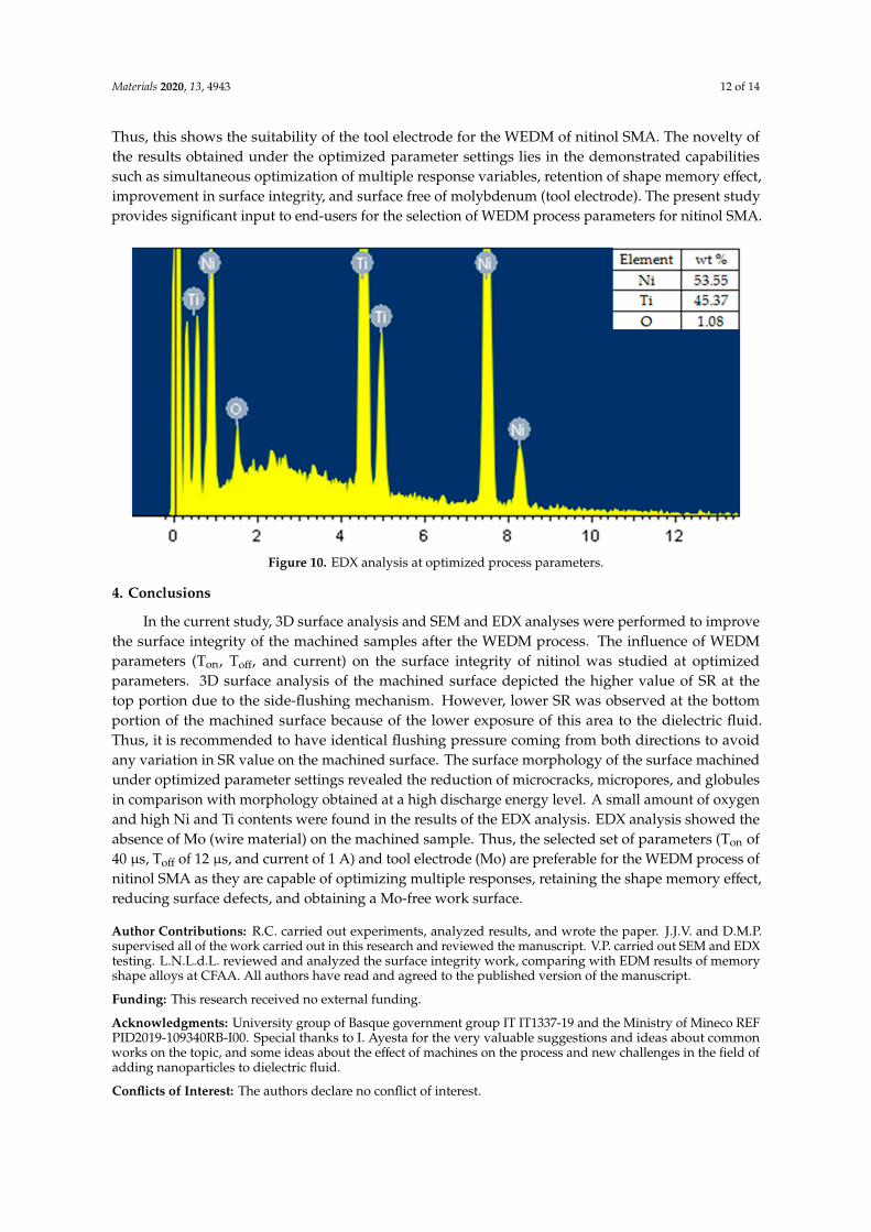
Materials 2020, 13, 4943 12 of 14
Thus, this shows the suitability of the tool electrode for the WEDM of nitinol SMA. The novelty ofthe results obtained under the optimized parameter settings lies in the demonstrated capabilitiessuch as simultaneous optimization of multiple response variables, retention of shape memory effect,improvement in surface integrity, and surface free of molybdenum (tool electrode). The present studyprovides significant input to end-users for the selection of WEDM process parameters for nitinol SMA.
Figure 10. EDX analysis at optimized process parameters.
4. Conclusions
In the current study, 3D surface analysis and SEM and EDX analyses were performed to improvethe surface integrity of the machined samples after the WEDM process. The influence of WEDMparameters (Ton, Toff, and current) on the surface integrity of nitinol was studied at optimizedparameters. 3D surface analysis of the machined surface depicted the higher value of SR at thetop portion due to the side-flushing mechanism. However, lower SR was observed at the bottomportion of the machined surface because of the lower exposure of this area to the dielectric fluid.Thus, it is recommended to have identical flushing pressure coming from both directions to avoidany variation in SR value on the machined surface. The surface morphology of the surface machinedunder optimized parameter settings revealed the reduction of microcracks, micropores, and globulesin comparison with morphology obtained at a high discharge energy level. A small amount of oxygenand high Ni and Ti contents were found in the results of the EDX analysis. EDX analysis showed theabsence of Mo (wire material) on the machined sample. Thus, the selected set of parameters (Ton of40 µs, Toff of 12 µs, and current of 1 A) and tool electrode (Mo) are preferable for the WEDM process ofnitinol SMA as they are capable of optimizing multiple responses, retaining the shape memory effect,reducing surface defects, and obtaining a Mo-free work surface.
Author Contributions: R.C. carried out experiments, analyzed results, and wrote the paper. J.J.V. and D.M.P.supervised all of the work carried out in this research and reviewed the manuscript. V.P. carried out SEM and EDXtesting. L.N.L.d.L. reviewed and analyzed the surface integrity work, comparing with EDM results of memoryshape alloys at CFAA. All authors have read and agreed to the published version of the manuscript.
Funding: This research received no external funding.
Acknowledgments: University group of Basque government group IT IT1337-19 and the Ministry of Mineco REFPID2019-109340RB-I00. Special thanks to I. Ayesta for the very valuable suggestions and ideas about commonworks on the topic, and some ideas about the effect of machines on the process and new challenges in the field ofadding nanoparticles to dielectric fluid.
Conflicts of Interest: The authors declare no conflict of interest.

Materials 2020, 13, 4943 13 of 14
References
1. Jani, J.M.; Leary, M.; Subic, A.; Gibson, M.A. A review of shape memory alloy research, applications andopportunities. Mater. Des. 2014, 56, 1078–1113. [CrossRef]
2. Ölander, A. An electrochemical investigation of solid cadmium-gold alloys. J. Am. Chem. Soc. 1932, 54, 3819–3833.[CrossRef]
3. Khanna, S.; Utsav; Patel, R.; Marathey, P.; Chaudari, R.; Vora, J.; Banerjee, R.; Ray, A.; Mukhopadhyay, I.Growth of titanium dioxide nanorod over shape memory material using chemical vapor deposition forenergy conversion application. Mater. Today Proc. 2020, 28, 475–479. [CrossRef]
4. Safranski, D.; Dupont, K.; Gall, K. Pseudoelastic NiTiNOL in Orthopaedic Applications. Shape Mem. Superelasticity2020, 6, 332–341. [CrossRef]
5. Yoneyama, T.; Miyazaki, S. Shape Memory Alloys for Biomedical Applications; Elsevier: Amsterdam,The Netherlands, 2009.
6. Hamann, I.; Hempel, U.; Rotsch, C.; Leimert, M. Biological Cell Investigation of Structured Nitinol Surfacesfor the Functionalization of Implants. Materials 2020, 13, 3264. [CrossRef]
7. Kulkarni, V.N.; Gaitonde, V.; Karnik, S.; Manjaiah, M.; Davim, J.P. Machinability Analysis and Optimizationin Wire EDM of Medical Grade NiTiNOL Memory Alloy. Materials 2020, 13, 2184. [CrossRef]
8. Rathi, P.; Ghiya, R.; Shah, H.; Srivastava, P.; Patel, S.; Chaudhari, R.; Vora, J. Multi-response Optimization ofNi55.8Ti Shape Memory Alloy Using Taguchi–Grey Relational Analysis Approach. In Innovations in SmartCities Applications Edition 2; Springer: Berlin/Heidelberg, Germany, 2020; pp. 13–23.
9. Lagoudas, D.; Rediniotis, O.K.; Khan, M.M.; Dassios, G.; I Fotiadis, D.; Massalas, C.V.; Kiriaki, K. Applicationsof shape memory alloys to bioengineering and biomedical technology. In Scattering Theory and BiomedicalEngineering Modelling and Applications; World Scientific: Singapore, 2000; pp. 195–207.
10. Chaudhari, R.; Vora, J.J.; Prabu, S.S.M.; Palani, I.A.; Patel, V.K.; Parikh, D.M.; De Lacalle, L.N.L. Multi-ResponseOptimization of WEDM Process Parameters for Machining of Superelastic Nitinol Shape-Memory AlloyUsing a Heat-Transfer Search Algorithm. Materials 2019, 12, 1277. [CrossRef]
11. Sheth, M.; Gajjar, K.; Jain, A.; Shah, V.; Patel, H.; Chaudhari, R.; Vora, J. Multi-objective Optimization ofInconel 718 Using Combined Approach of Taguchi—Grey Relational Analysis. In Advances in MechanicalEngineering; Springer: Berlin/Heidelberg, Germany, 2020; pp. 229–235.
12. Chaudhari, R.; Vora, J.J.; Pramanik, A.; Parikh, D. Optimization of Parameters of Spark Erosion BasedProcesses. In Spark Erosion Machining; CRC Press: Boca Raton, FL, USA, 2020; pp. 190–216.
13. Chaudhari, R.; Vora, J.; Parikh, D.M.; Wankhede, V.; Khanna, S. Multi-response Optimization of WEDMParameters Using an Integrated Approach of RSM–GRA Analysis for Pure Titanium. J. Inst. Eng. (India)Ser. D 2020, 101, 117–126. [CrossRef]
14. Lalwani, V.; Sharma, P.; Pruncu, C.I.; Unune, D.R. Response Surface Methodology and Artificial NeuralNetwork-Based Models for Predicting Performance of Wire Electrical Discharge Machining of Inconel 718Alloy. J. Manuf. Mater. Process. 2020, 4, 44.
15. Theisen, W.; Schuermann, A. Electro discharge machining of nickel-titanium shape memory alloys. Mater. Sci.Eng. A 2004, 378, 200–204. [CrossRef]
16. Majumder, H.; Maity, K. Application of GRNN and multivariate hybrid approach to predict and optimizeWEDM responses for Ni-Ti shape memory alloy. Appl. Soft Comput. 2018, 70, 665–679. [CrossRef]
17. Soni, H.; Sannayellappa, N.; Rangarasaiah, R.M. An experimental study of influence of wire electro dischargemachining parameters on surface integrity of TiNiCo shape memory alloy. J. Mater. Res. 2017, 32, 3100–3108.[CrossRef]
18. Tosun, N. The effect of the cutting parameters on performance of WEDM. KSME Int. J. 2003, 17, 816–824.[CrossRef]
19. Sánchez, J.A.; Ortega, N.; De Lacalle, L.N.L.; Lamikiz, A.; Marañon, J.A.; De Lacalle, L.N.L.; Lamikiz, A.Analysis of the electro discharge dressing (EDD) process of large-grit size cBN grinding wheels. Int. J. Adv.Manuf. Technol. 2005, 29, 688–694. [CrossRef]
20. Reolon, L.W.; Laurindo, C.A.H.; Torres, R.D.; Amorim, F.L. WEDM performance and surface integrity ofInconel alloy IN718 with coated and uncoated wires. Int. J. Adv. Manuf. Technol. 2018, 100, 1981–1991.[CrossRef]

Materials 2020, 13, 4943 14 of 14
21. Chaudhari, R.; Vora, J.J.; Prabu, S.S.M.; Palani, I.A.; Patel, V.K.; Parikh, D.M. Pareto optimization of WEDMprocess parameters for machining a NiTi shape memory alloy using a combined approach of RSM and heattransfer search algorithm. Adv. Manuf. 2019, 40, 1–17. [CrossRef]
22. Chaudhari, R.; Vora, J.J.; Patel, V.; De Lacalle, L.N.L.; Parikh, D.M. Surface Analysis ofWire-Electrical-Discharge-Machining-Processed Shape-Memory Alloys. Materials 2020, 13, 530.
23. Tosun, N.; Pihtili, H. The Effect of Cutting Parameters on Wire Crater Sizes in Wire EDM. Int. J. Adv.Manuf. Technol. 2003, 21, 857–865. [CrossRef]
24. Bisaria, H.; Shandilya, P. Experimental investigation on wire electric discharge machining (WEDM) ofNimonic C-263 superalloy. Mater. Manuf. Process. 2018, 34, 83–92. [CrossRef]
25. Ho, K.; Newman, S.; Rahimifard, S.; Allen, R. State of the art in wire electrical discharge machining (WEDM).Int. J. Mach. Tools Manuf. 2004, 44, 1247–1259. [CrossRef]
26. Ghanem, F.; Braham, C.; Sidhom, H. Influence of steel type on electrical discharge machined surface integrity.J. Mater. Process. Technol. 2003, 142, 163–173. [CrossRef]
27. Jangra, K.K. An experimental study for multi-pass cutting operation in wire electrical discharge machiningof WC-5.3% Co composite. Int. J. Adv. Manuf. Technol. 2014, 76, 971–982. [CrossRef]
28. Magabe, R.; Sharma, N.; Gupta, K.; Davim, J.P. Modeling and optimization of Wire-EDM parameters formachining of Ni55.8Ti shape memory alloy using hybrid approach of Taguchi and NSGA-II. Int. J. Adv.Manuf. Technol. 2019, 102, 1703–1717. [CrossRef]
29. Sharma, N.; Gupta, K.; Davim, J.P. On wire spark erosion machining induced surface integrity of Ni55.8Tishape memory alloys. Arch. Civ. Mech. Eng. 2019, 19, 680–693. [CrossRef]
30. Bisaria, H.; Shandilya, P. The machining characteristics and surface integrity of Ni-rich NiTi shape memoryalloy using wire electric discharge machining. Proc. Inst. Mech. Eng. Part C J. Mech. Eng. Sci. 2018,233, 1068–1078. [CrossRef]
31. Pirani, C.; Iacono, F.; Generali, L.; Sassatelli, P.; Nucci, C.; Lusvarghi, L.; Gandolfi, M.G.; Prati, C. HyFlexEDM: Superficial features, metallurgical analysis and fatigue resistance of innovative electro dischargemachined NiTi rotary instruments. Int. Endod. J. 2015, 49, 483–493. [CrossRef]
32. Azam, M.; Jahanzaib, M.; Abbasi, J.A.; Abbas, M.; Wasim, A.; Hussain, S. Parametric analysis of recast layerformation in wire-cut EDM of HSLA steel. Int. J. Adv. Manuf. Technol. 2016, 87, 713–722. [CrossRef]
33. Newton, T.R.; Melkote, S.N.; Watkins, T.; Trejo, R.M.; Reister, L. Investigation of the effect of processparameters on the formation and characteristics of recast layer in wire-EDM of Inconel 718. Mater. Sci. Eng. A2009, 513, 208–215. [CrossRef]
Publisher’s Note: MDPI stays neutral with regard to jurisdictional claims in published maps and institutionalaffiliations.
© 2020 by the authors. Licensee MDPI, Basel, Switzerland. This article is an open accessarticle distributed under the terms and conditions of the Creative Commons Attribution(CC BY) license (http://creativecommons.org/licenses/by/4.0/).


![Multi Objective Optimization of WEDM Process Parameters ... ID-672018125.pdf · the effect of WEDM parameters on various performance parameters [1]. Keeping this in view, the present](https://img.pdfslide.net/doc/110x75/5f239eb3730f3802f0081483/multi-objective-optimization-of-wedm-process-parameters-id-the-effect-of.jpg)