Embed Size (px)
Citation preview
NASA TECHNICAL NOTE
CO
^~r-x
NASA TN D-7423
c
EFFECTS OF NUCLEAR RADIATIONON A HIGH-RELIABILITYSILICON POWER DIODEIV - Analysis of Reverse Bias Characteristics
by Julian F. Been
Lewis Research Center
Cleveland, Ohio 44135
NATIONAL AERONAUTICS AND SPACE ADMINISTRATION • WASHINGTON, D. C • OCTOBER 1973
https://ntrs.nasa.gov/search.jsp?R=19730023821 2018-06-11T13:55:10+00:00Z
1. Report No.
NASA TN D-7423
2. Government Accession No. 3. Recipient's Catalog No.-
4. Title and Subtitle EFFECTS OF NUCLEAR RADIATION ON A
HIGH-RELIABILITY SILICON POWER DIODEIV - ANALYSIS OF REVERSE BIAS CHARACTERISTICS
5. Report Date
October 19736. Performing Organization Code
7. Author(s)
Julian F. Been
8. Performing Organization Report No.
E-7362
9. Performing Organization Name and Address
Lewis Research CenterNational Aeronautics and Space AdministrationCleveland, Ohio 44135
10. Work Unit No.
502-2511. Contract or Grant No.
12. Sponsoring Agency Name and Address
National Aeronautics and Space AdministrationWashington, D. C. 20546
13. Type of Report and Period Covered
Technical Note14. Sponsoring Agency Code
15. Supplementary Notes
16. Abstract
The effects of nuclear radiation on the reverse bias electrical characteristics of one hundredsilicon power diodes were investigated. It was found that on a percentage basis the changes inreverse currents were large but, due to very low initial values, this electrical characteristicwould hot be the limiting factor in use of these diodes. These changes were interpreted interms of decreasing minority carrier lifetimes as related to generation-recombination currents.The magnitudes of reverse voltage breakdown were in most instances unaffected by irradiation.
17. Key Words (Suggested by Author(sl)
Radiation effectsNuclear radiationSilicon diodesElectrical characteristics
18. Distribution Statement
Unclassified - unlimited
19. Security Qassif. (of this report)
Unclassified20. Security Classif. (of this page)
Unclassified21. No. of Pages
34
22. Price*
Domestic, S3.00Foreign, $5.50
"For sale by the National Technical Information Service, Springfield, Virginia 22151
EFFECTS OF NUCLEAR RADIATION ON A HIGH-RELIABILITY
SI LI CON POWER DIODE
IV - ANALYSIS OF REVERSE BIAS CHARACTERISTICS
by Julian F. Been
Lewis Research Center
SUMMARY
The effects of nuclear radiation on the reverse bias electrical characteristics ofone hundred, 35-ampere, 600-volt peak inverse, high-reliability silicon power diodeswere investigated. The diodes were irradiated in the NASA Plum Brook Nuclear Reac-tor for a total time of approximately 480 hours. The resultant fast neutron (0.1 MeV
13and above) fluence was 5x10 neutrons per square centimeter and a gamma dose off3x10 rads (C). Diodes before irradiation had very low reverse currents, sharp break-down knees but considerable spread in voltage at a given current among the diodes.Some diode curves showed irregularities in that as the voltage was increased the currentincreased in an uneven manner. This generally occurred in the higher voltages (100 Vand up). The effect of radiation was to increase the reverse currents for given voltagesup to approximately 100 volts. Above this value, approximately 30 percent showed de-creases in reverse currents with radiation. These decreases were generally associatedwith the irregular shaped curves in that irradiation tended to minimize the irregularshapes. Irradiating the diodes at different temperatures and in different operatingmodes made no notable difference in the reverse characteristics. The reverse voltagebreakdown knee remained identifiable although the knee became more rounded. Themagnitude of avalanche voltage in general remained relatively constant.
A theoretical curve for preirradiated diodes was calculated, and compared to ex-perimental results. An estimate was made of Hie effects or radiation at the lower volt-ages where fair agreement was obtained. At higher voltages (above 100 V) the effects ofradiation were unpredictable due to the irregular curves. An attempt was made withlittle success to correlate the irregularly shaped curves, (and associated effects of ir-radiation on them), with other changes in electrical characteristics such as change incapacitance and forward voltage drop.
The results of this test allow a diode to be made more radiation tolerant by utilizingthe trade-offs in the very low reverse currents and high breakdown voltages for im-proved forward electrical characteristics. '- ' . "
INTRODUCTION
Whenever semiconductors are used as part of a nuclear electric power generatingsystem, it is generally accepted that the semiconductors are the most sensitive com-ponents to nuclear radiation in that system. In space power applications where it maynot be possible to locate or shield components to obtain radiation of acceptable levels,testing becomes necessary to determine how much those semiconductors, contemplatedfor system use, will tolerate before failure. Generally it is desirable to know morethan the fact that a device failed to perform its intended function in a circuit. If it canbe determined how each electrical characteristic changed, steps can be taken to improvea particular characteristic. This can be accomplished through correlating the basicparameters of the device to its electrical characteristics and altering those parametersin such a way as to improve that particular electrical characteristic with respect toradiation damage. Changes in the basic parameters or geometry of the device to ac-commodate one electrical characteristic to radiation effects generally means a trade-off in another electrical characteristic. It is therefore necessary to investigate severalof the important electrical characteristics and the effects of radiation on them to deter-mine the most feasible way to improve radiation tolerance.
The discussion and analysis in this report pertains to the reverse biased electricalcharacteristics, that is, the reverse currents and breakdown voltages and the effects ofnuclear radiation on them. Considerable work has been done by investigators in thearea of reverse biased junctions (refs. 1 and 2) and the effects of radiation on them(ref. 3). Like the forward electrical characteristics (ref. 4) the mechanisms governingthe reverse current as a function of voltage depend upon the basic parameters and geom-etry of the silicon chip. Of the three components of the reverse current; diffusion,generation-re combination and surface, the first two have established relations betweenthe basic device parameters including geometry of the device and the current compo-nents. The surface component is less defined and is therefore less predictable. Thisinvestigation attempted to compare calculated with experimental values of the reverseelectrical characteristics of a 35-ampere, 600-volt peak inverse (PIV) silicon powerdiode and to examine the effects of radiation on them.
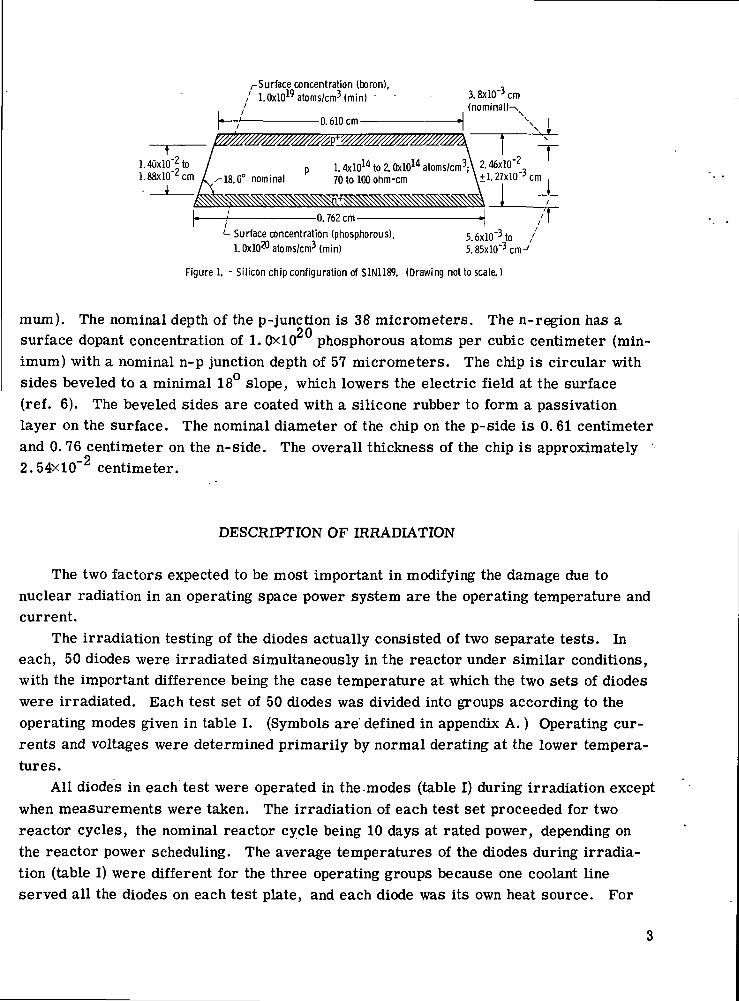
DESCRIPTION OF DIODES TESTED
The diode investigated was an S1N1189. The prefix "S" in the part number indi-cates that the diode passed the NASA Marshall Space Flight Center screening and per-formance specification (ref. 5). The silicon chip configuration is shown in figure 1 andhas an n+-p-p+-type junction prepared by a double-diffusion process. The base region
14 14p-material is doped to 1. 4x10 to 2. 0x10 boron.atoms per cubic centimeters (mini-
/-Surface concentration (boron), ,/ l.OxlO19atoms/cm3(mini - - 3.8xKPcm
/ t (nominal)-•f 0.610cm
1.40x10⁻² to / 1.4xlOMto2.0xl014atoms/cm3;\2.46xlO-2
1.88x10 'cm y( ig.c0 nominal 70 to 100 ohm-cm \±1.27x10 J cm .
_1 /
-0.762 cm J /|
<- Surface concentration (phosphorous), 5.6xlO"3to '1. OxlO20 atoms/cm3 (min) 5.85x10"3 cm^'
Figure 1. - Silicon chip configuration of S1N1189. (Drawing not to scale. )
mum). The nominal depth of the p-junction is 38 micrometers. The n-region has asurface dopant concentration of 1.0x10 phosphorous atoms per cubic centimeter (min-imum) with a nominal n-p junction depth of 57 micrometers. The chip is circular withsides beveled to a minimal 18 slope, which lowers the electric field at the surface(ref. 6). The beveled sides are coated with a silicone rubber to form a passivationlayer on the surface. The nominal diameter of the chip on the p-side is 0. 61 centimeterand 0. 76 centimeter on the n-side. The overall thickness of the chip is approximately2.54*10~2 centimeter.
DESCRIPTION OF IRRADIATION
The two factors expected to be most important in modifying the damage due tonuclear radiation in an operating space power system are the operating temperature andcurrent.
The irradiation testing of the diodes actually consisted of two separate tests. Ineach, 50 diodes were irradiated simultaneously in the reactor under similar conditions,with the important difference being the case temperature at which the two sets of diodeswere irradiated. Each test set of 50 diodes was divided into groups according to theoperating modes given in table I. (Symbols are defined in appendix A.) Operating cur-rents and voltages were determined primarily by normal derating at the lower tempera-tures.
All diodes in each test were operated in the modes (table I) during irradiation exceptwhen measurements were taken. The irradiation of each test set proceeded for tworeactor cycles, the nominal reactor cycle being 10 days at rated power, depending onthe reactor power scheduling. The average temperatures of the diodes during irradia-tion (table I) were different for the three operating groups because one coolant lineserved all the diodes on each test plate, and each diode was its own heat source. For
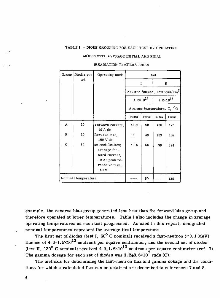
TABLE I. - DIODE GROUPING FOR EACH TEST BY OPERATING
MODES WITH AVERAGE INITIAL AND FINAL
IRRADIATION TEMPERATURES
Group
A
B
C
Diodes perset
10
10
30
Operating mode
Forward current,10 A dc
Reverse bias,100 V dc
ac rectification;average for-ward current,10 A; peak re-verse voltage,150 V
Nominal temperature
Set
I nn
Neutron fluence, neutrons/cm
4. 6X10¹³ 4. OxlO13
Average temperature, T, °C
Initial
48.5
38
50.5
Final
60
43
66
60
Initial
106
103
99
---
Final
125
102
124
120
example, the reverse bias group generated less heat than the forward bias group andtherefore operated at lower temperatures. Table I also includes the change in averageoperating temperatures as each test progressed. As used in this report, designatednominal temperatures represent the average final temperature.
The first set of diodes (test I, 60° C nominal) received a fast-neutron (£0.1 MeV)13fluence of 4. 6±1. 5x10 neutrons per square centimeter, and the second set of diodes
(test n, 120° C nominal) received 4.9±1.6xlO neutrons per square centimeter (ref. 7).n
The gamma dosage for each set of diodes was 3.2±0. 6x10 rads (C).The methods for determining the fast-neutron flux and gamma dosage and the condi-
tions for which a calculated flux can be obtained are described in references 7 and 8.
DISCUSSION AND ANALYSIS
Current- Voltage Calculations
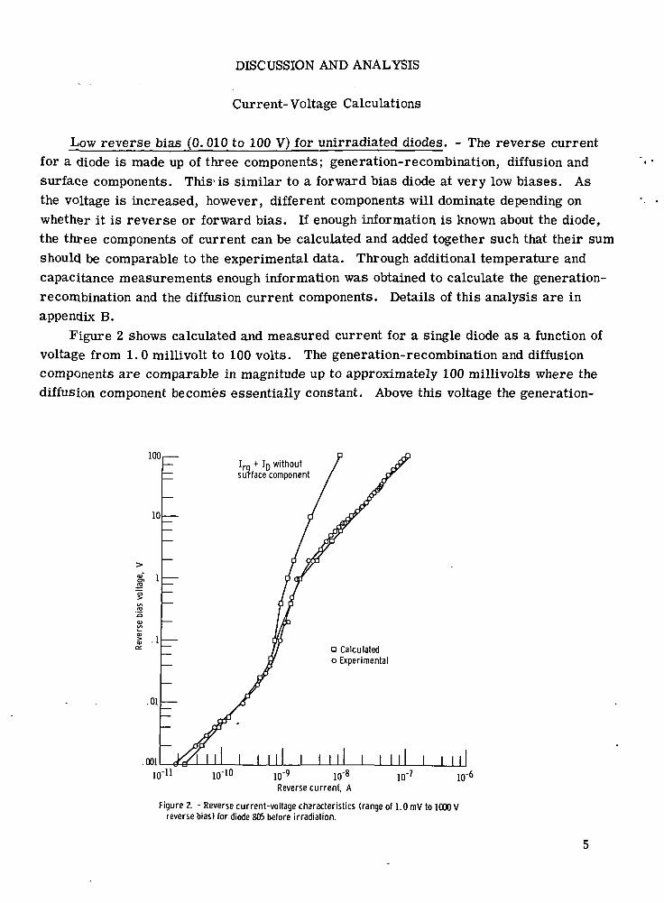
reverse bias (0. 010 to 100 V) for unirradiated diodes. - The reverse currentfor a diode is made up of three components; generation-recombination, diffusion andsurface components. This1 is similar to a forward bias diode at very low biases. Asthe voltage is increased, however, different components will dominate depending onwhether it is reverse or forward bias. If enough information is known about the diode,the three components of current can be calculated and added together such that their sumshould be comparable to the experimental data. Through additional temperature andcapacitance measurements enough information was obtained to calculate the generation-recombination and the diffusion current components. Details of this analysis are inappendix B.
Figure 2 shows calculated and measured current for a single diode as a function ofvoltage from 1. 0 millivolt to 100 volts. The generation-recombination and diffusioncomponents are comparable in magnitude up to approximately 100 millivolts where thediffusion component becomes essentially constant. Above this voltage the generation-
Reverse current, A
Figure 2. - Reverse current-voltage characteristics (range of 1.0 mV to 1000 Vreverse bias) for diode 805 before irradiation.
recombination component becomes much larger than the diffusion component. The cal-culations for the generation-re combination current were based on the depletion regionwidth increasing as the applied voltage to the one half power above an applied voltage of1 volt. This was in agreement with capacitance-voltage measurements.
The magnitude of the calculated current components and the shape of the curves arecomparable to the experimental results at very low voltages. At higher voltages, how-ever, the added components of generation-re combination and diffusion are considerablysmaller than the experimental values. It can be postulated that a large part of the differ-ence in the calculated and the experimental values was due to a surface component sinceabove approximately 1.0 volt the current was almost a linear function of voltage. Thisis the type of relation that would be expected from a resistive surface leakage.
Q
When a resistive current component was calculated, based on an assumed 10 ohmssurface resistance for this particular diode, there was good agreement with experimen-tal values including the higher voltages up to 100 volts, as seen in figure 2. Even as-suming a fair degree of uniformity in the fabrication process, it would not be expectedthat this surface resistance would be the same for each diode. The surface componentof current therefore might be the least predictable of the three current components andtherefore contribute to the large variation of total reverse currents observed among thediodes.
Effects of radiation damage at low reverse bias. - The direction of change in thereverse current due to irradiation at low reverse bias (100 V and below) is consistentand predictable. The magnitude of change, however, is not as consistent nor predict-able due to the variation in data from individual diodes, and to the five orders of volt-ages and current considered, as figure 2. The fact that the minority carrier lifetimedecreases due to radiation induced recombination centers has been established (refs. 3,9 and 10). The amount of decrease is dependent upon a number of factors such as theenergy of the incident radiation, type of radiation, amount of radiation, and so forth.Examination of equation (Bl) would indicate that (1) generation-recombination componentof current should increase and (2) it should increase inversely proportional to the de-creasing minority carrier lifetime J-r' T . The change in the effective minority car-rier lifetime was determined in appendix C by measuring the change in reverse currentduring irradiation on a sample group and calculating a damage constant K_ for silicon.sThe measurements were made at 100 volts reverse bias to minimize the effects, atlower voltages, of the diffusion component of current, and yet stay below those voltageswhere the current varied irregularly with increasing voltages. There was considerablevariation in the damage constant K and therefore in the effective minority carrierlifetime r *,. The average change in r .* for the low temperature cycles was approx-imately a factor of ten; however, the reff for individual diodes varied considerablymore. This indicates that caution must be used when applying these sample calculationsto individual diodes. However, applying these results to equation (Bl); the generation-
recombination current should increase by some factor of approximately ten. The diffu-sion component (eq. (B2)), however, will be affected less, that is, through the relationL = JDr, so that the diffusion component will increase by the factor WT
after/Tbefore'
When both components are considered at 100 volts, if the increase is due to the changein effective T .., the total reverse current should increase by approximately a factorof ten. Comparing this change with the diode considered previously (fig. 3), there isreasonable agreement at this bias.
Below 100 volts bias the change in reverse current was generally greater than afactor of ten. Although no measurements were made to check the effects of radiationon the surface of the semiconductor chip, it is possible that ionization paths or channelsformed which would alter the reverse electrical characteristics. Since these surfacestates can have different generation-recombination rates (ref. 2), it is possible that thegreater changes than predicted were due to these surface effects.
The curve also straightens out with radiation such that it is a much smoother curve
10-Reverse current, A
Figure 3. - Curves showing effects of radiation on reverse current-voltage characteristics (range of 1.0 mV to1000 V reverse bias) for diode 805. (Neutron fluence for one reactor cycle is approximately 2.5x10^3 neutrons/rm' 1cms)
1/2and more closely follows a V ' slope, as would be expected above approximately1. 0 volts bias. This smoothing is principally due to the fact that with the decreasingminority carrier lifetime, the diffusion component becomes a considerably smallerportion of the total reverse current at the lower voltages.
High reverse bias (above 100 V) for unirradiated diodes. - Some general statementscan be made as to the current-voltage characteristics at higher voltages which are con-sidered to be more nearly the operating voltages of the device: (1) all preirradiated
fi 7reverse currents were very low (10~ to 10" A) at the rated voltage of 600 volts;(2) all diodes had relatively sharp avalanche breakdown voltage; and (3) the reversebias curves tend to group into two classes, normal and irregular. The curves whichwere considered normal were those whose currents increased smoothly as the reverse
S.OxlO'4
Diode
4.0767
773
770
3.0
2.0
1.0
69
200 400 600 800 1000Reverse bias voltage, V
1200 1400 1600
Figure 4. - X-Y plot of reverse current as a function of applied voltage including avalancheregion for diodes 767, 769, 770, and 773 before irradiation.
5.0x10"
4.0
3.0
2.0
1.0
773
Diode
767
770
769
400 600 800 1000Reverse bias voltage, V
1200 1400 1600
Figure 5. - X-Y plot of reverse current as a function of applied voltage including avalancheregion for diodes 767, 769, 770, and 773 before irradiation. Expanded current axis.
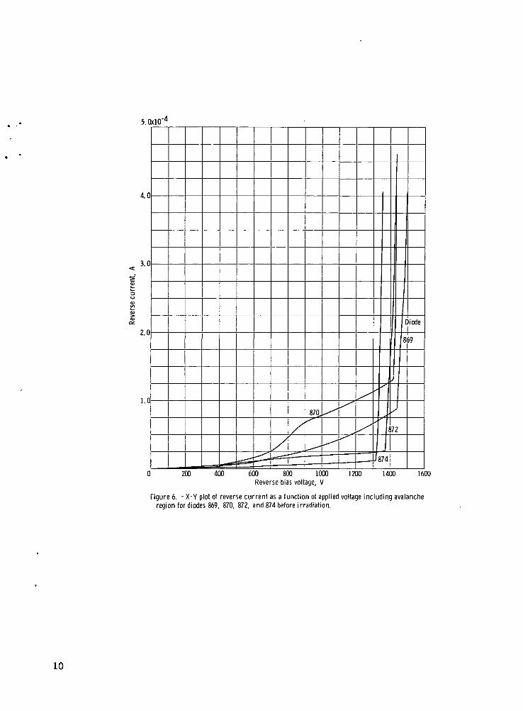
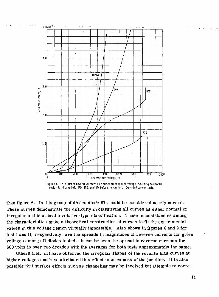
voltage was increased, as one would expect from theory. The irregular curves wereidentified as those whose currents vary unevenly as the reverse voltage is increased.Both classes, however, had relatively sharp breakdown knees. Figures 4 and 5 areconsidered to be normal curves. Both figures are for the same group of diodes but
-5figure 5 has the current axis expanded by a decade to 10" amperes. Figure 4 showsthe higher breakdown voltages better while figure 5 shows the lower voltage-currentsmore clearly. It can be seen that in the expanded scales (fig. 5) diode 770 actuallyshows some irregularity in its characteristics whereas the rest have a relative smoothslope. Figures 6 and 7 are two sets of similar curves for the group of diodes consider-ed to be irregular. Again figure 6 illustrates the higher voltage regions better thanfigure 7, whereas the curves of figure 7 show the lower voltage curve shapes better
s.Qxio'4
400 600 800 1000Reverse bias voltage, V
1200 1400 1600
Figure 6. - X-Y plot of reverse current as a function of applied voltage including avalancheregion for diodes 869, 870, 872, and 874 before irradiation.
10
"5.0x10"
4.0
3.0
2.0
i
Diode
_ _ /
/869872
874
; 600 800 10001 Reverse bias voltage, V
1200 1400 1600
Figure 7. - X-Y plot of reverse current as a function of applied voltage including avalancheregion for diodes 869, 870, 872, and 874 before irradiation. Expanded current axis.
than figure 6. In this group of diodes diode 874 could be considered nearly normal.These curves demonstrate the difficulty in classifying all curves as either normal orirregular and is at best a relative-type classification. These inconsistancies amongthe characteristics make a theoretical construction of curves to fit the experimental
. values in this voltage region virtually impossible. Also shown in figures 8 and.9 fortest I and II, respectively, are the spreads in magnitudes of reverse currents for given^voltages among all diodes tested. It can be seen the spread in reverse currents for600 volts is over two decades with the averages for both tests approximately the same.
Others (ref. 11) have observed the irregular shapes of the reverse bias curves athigher voltages and have attributed this effect to uneveness of the junction. It is alsopossible that surface effects such as channeling may be involved but attempts to corre-
11
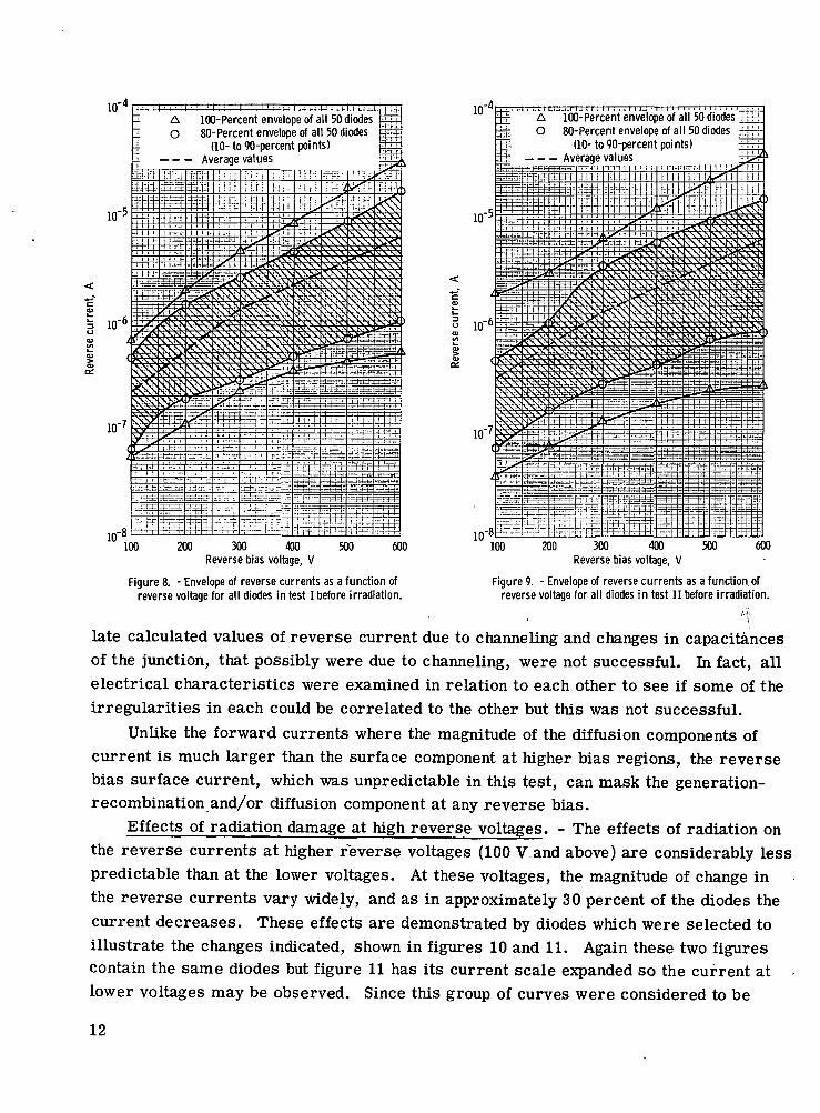
10',-4A 100-Percent envelope of all 50 diodesO 80-Percent envelope of all 50 diodes
(10- to 90-percent points)I Average values
'•-\iJe^,J\-
isoc.
10,-4 A 100-Percent envelope of all 50 diodes TTTTO 80-Percent envelope of all 50 diodes
(10-to 90-percent points)i|fj Average values**** I I-M--I3-M I I I M-i-fTl I I
sO>01
200 300 400 500Reverse bias voltage, V
600 100 200 300 400 500
Reverse bias voltage, V
Figure 8. - Envelope of reverse currents as a function ofreverse voltage for all diodes in test I before irradiation.
Figure 9. - Envelope of reverse currents as a function,ofreverse voltage for all diodes in test II before irradiation.
late calculated values of reverse current due to channeling and changes in capacitancesof the junction, that possibly were due to channeling, were not successful. In fact, allelectrical characteristics were examined in relation to each other to see if some of theirregularities in each could be correlated to the other but this was not successful.
Unlike the forward currents where the magnitude of the diffusion components ofcurrent is much larger than the surface component at higher bias regions, the reversebias surface current, which was unpredictable in this test, can mask the generation-recombination and/or diffusion component at any reverse bias.
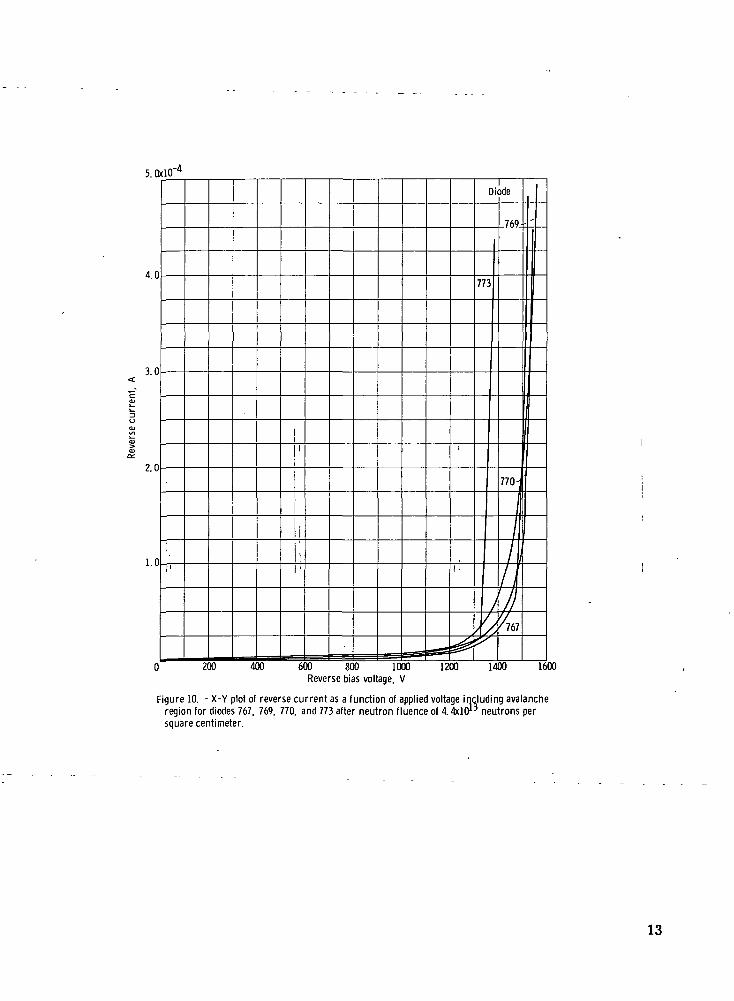
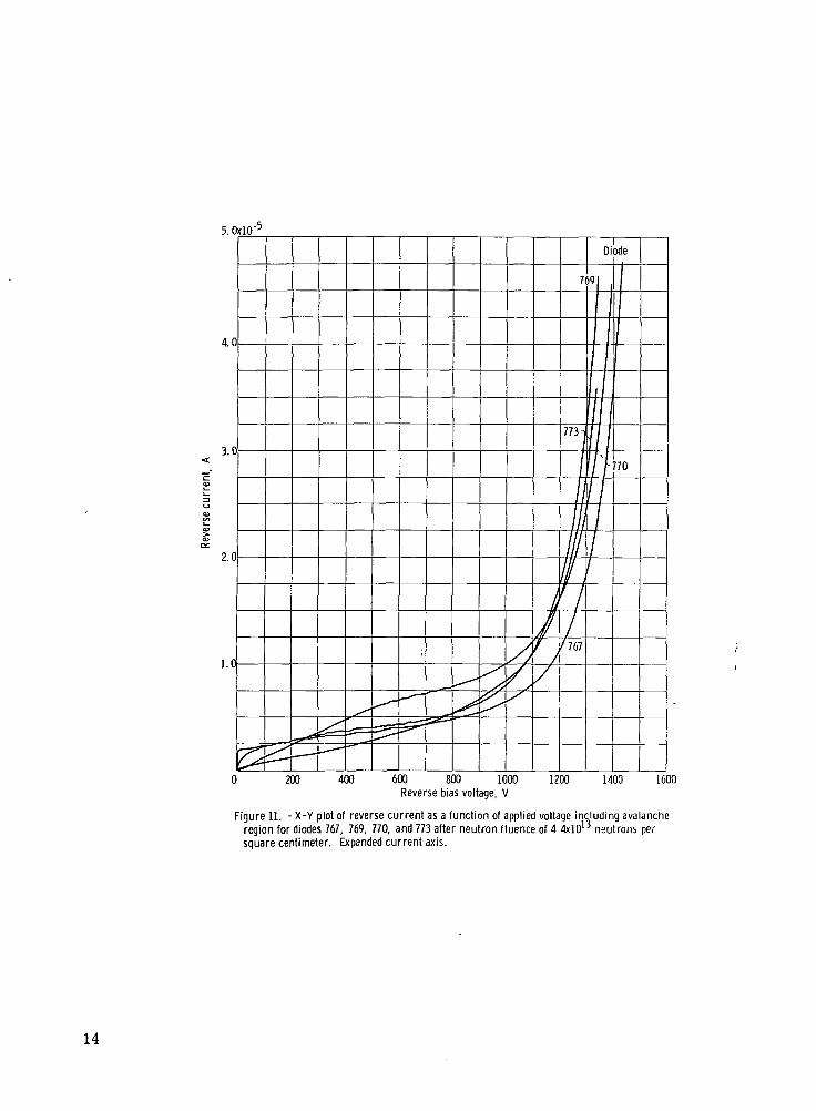
Effects of radiation damage at high reverse voltages. - The effects of radiation onthe reverse currents at higher reverse voltages (100 V and above) are considerably lesspredictable than at the lower voltages. At these voltages, the magnitude of change inthe reverse currents vary widely, and as in approximately 30 percent of the diodes thecurrent decreases. These effects are demonstrated by diodes which were selected toillustrate the changes indicated, shown in figures 10 and 11. Again these two figurescontain the same diodes but figure 11 has its current scale expanded so the current atlower voltages may be observed. Since this group of curves were considered to be
12
5.0x10
1.0
200 400 600 800 1000Reverse bias voltage, V
1200 1400 1600
Figure 10. - X-Y plot of reverse current as a function of applied voltage including avalancheregion for diodes 767, 769, 770, and 773 after neutron fluence of 4.4x10^ neutrons persquare centimeter.
13
5.0x10
4.0
200 400 600 800 1000Reverse bias voltage, V
1200 1400 1600
Figure 11. - X-Y plot of reverse current as a function of applied voltage including avalancheregion for diodes 767, 769, 770, and 773 after neutron fluence of 4 4x10^ neutrons persquare centimeter. Expanded current axis.
14
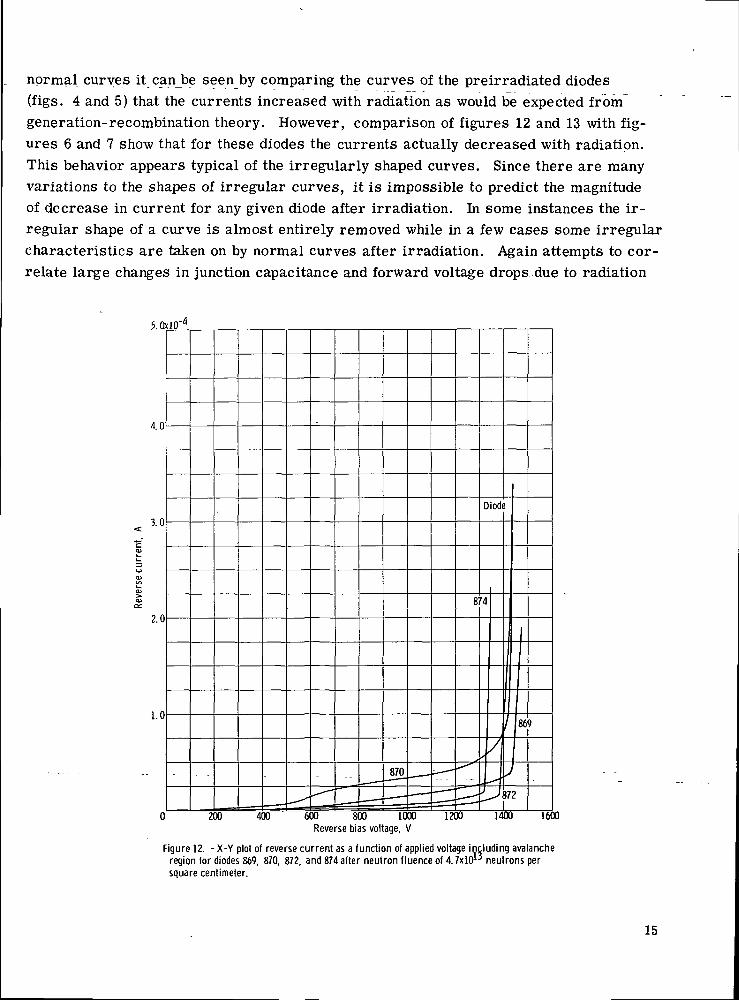
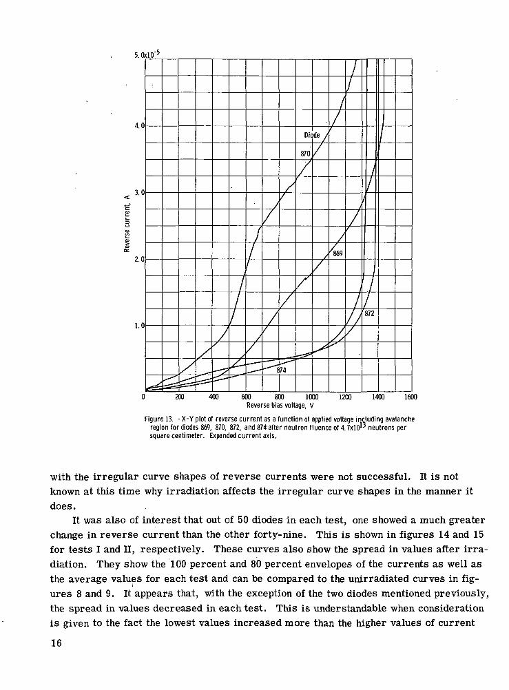
normal curves it can be seen by comparing the curves of the preirradiated diodes(figs. 4 and 5) that the currents increased with radiation as would be expected frbnfgeneration-recombination theory. However, comparison of figures 12 and 13 with fig-ures 6 and 7 show that for these diodes the currents actually decreased with radiation.This behavior appears typical of the irregularly shaped curves. Since there are manyvariations to the shapes of irregular curves, it is impossible to predict the magnitudeof decrease in current for any given diode after irradiation. In some instances the ir-regular shape of a curve is almost entirely removed while in a few cases some irregularcharacteristics are taken on by normal curves after irradiation. Again attempts to cor-relate large changes in junction capacitance and forward voltage drops due to radiation
5. OxlO"4
1.0
200 400 1200 1400 1600Reverse bias voltage, V
Figure 12. - X-Y plot of reverse current as a function of applied voltage including avalancheregion for diodes 869, 870, 872, and 874 after neutron fluence of 4.7x10" neutrons persquare centimeter.
15
5. QxlO-5
4.0Diode
870
77L
3.0
2.0
i.o LL 872
200 400 600 800 1000Reverse bias voltage, V
1200 1400 1600
Figure 13. - X-Y plot of reverse current as a function of applied voltage including avalancheregion for diodes 869, 870, 872, and 874 after neutron fluence of 4.7x10^ neutrons persquare centimeter. Expanded current axis.
with the irregular curve shapes of reverse currents were not successful. It is notknown at this time why irradiation affects the irregular curve shapes in the manner itdoes.
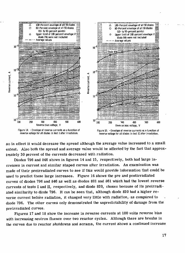
It was also of interest that out of 50 diodes in each test, one showed a much greaterchange in reverse current than the other forty-nine. This is shown in figures 14 and 15for tests I and II, respectively. These curves also show the spread in values after irra-diation. They show the 100 percent and 80 percent envelopes of the currents as well asthe average values for each test and can be compared to the unirradiated curves in fig-ures 8 and 9. It appears that, with the exception of the two diodes mentioned previously,the spread in values decreased in each test. This is understandable when considerationis given to the fact the lowest values increased more than the higher values of current
16
A 100-Percent envelope of all 50diodesO 80-Percent envelope of all 50 diodes Prt
(10- to 90-percent points) |O Upper limit of 100-percent envelope if K
diode 796 were not included j||H Average values
10,-4
A 100-Percent envelope of allSO diodes §§O 80-Percent envelope of all 50 diodes
(10-to 90-percent points)O Upper limit of 100-percent envelope if jjj
diode 846 were not includedAverage values
100 200 300 400Reverse bias voltage, V
500 600
Figure 14. - Envelope of reverse currents as a function ofreverse voltage for all diodes in test I after irradiation.
TOO 400Reverse Bias voltage, V
Figure 15. - Envelope of reverse currents as a function ofreverse voltage for all diodes in test II after irradiation.
so in effect it would decrease the spread although the average value increased to a smallextent. Also both the spread and average value would be affected by the fact that approx-imately 30 percent of the currents decreased with radiation.
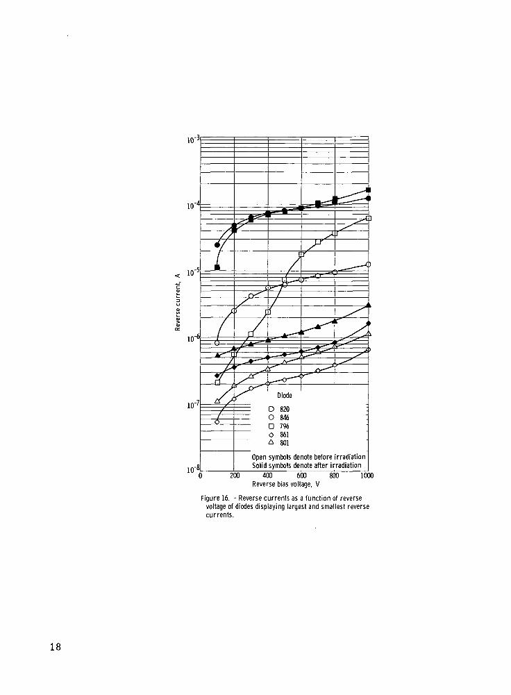
Diodes 796 and 846 shown in figures 14 and 15, respectively, both had large in-creases in current and similar shaped curves after irradiation. An examination wasmade of their preirradiated curves to see if this would provide information that could beused to predict these large increases. Figure 16 shows the pre and postirradiatedcurves of diodes 796 and 846 as well as diodes 801 and 861 which had the lowest reversecurrents of tests I and H, respectively, and diode 820, chosen because of its preirradi-ated similarity to diode 796. It can be seen that, although diode 820 had a higher re-verse current before radiation, it changed very little with radiation, as compared todiode 796. The other curves only demonstrated the unpredictability of damage from thepreirradiated curves.
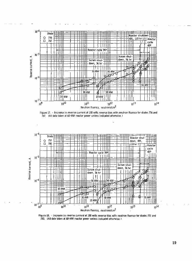
Figures 17 and 18 show the increase in reverse currents at 100 volts reverse biaswith increasing neutron fluence over two reactor cycles. Although there are breaks inthe curves due to reactor shutdowns and scrams, the current shows a continued increase
17
10,-3
10,-5
10r6
10,-7
10'
L
Z Z
Diode
D 820O 846D 796O 861& 801
Open symbols denote before irradiationSolid symbols denote after irradiation
200 400 600Reverse bias voltage, V
800 1000
Figure 16. - Reverse currents as a function of reversevoltage of diodes displaying largest and smallest reversecurrents.
18
ID''
10,-5
o• a
Diode7576
I.
O
11
-^•"*"
.:^^^
OMWII
^•"**
^— •
. >
Scr;
5(
4
--4*-•• ^
JOMW
o r eyc
m shu, 36h
IM\
*#.}
|t
£
11
V
—>
jf-/II(V
e39P
t- '
[}
£3 ^yD
3
W
50 MW,_
iiJT0""^fc
;ilij —
OMW
otdm
— •
K41
ram MIUwn, 56 h
, — f
-f
•7
J,-
>•
sactor st-S, 110 h
1
utdi -,/
j(t /
rrO r-r
• i PI nkc
^^4=-t? — \-50
}W
n1
J
*;
MV
lRicy10
il
v
if-
ft1 1 1
actorcleP
10,-6
10-7
1010 1011 1012
Neutron fluence, neutrons/cm'10,13 10,14
Figure 17. - Increase in reverse current at 100 volts reverse bias with neutron fluence for diodes 756 and767. (All data taken at 60-MW reactor power unless indicated otherwise.)
10"
'- O- D
.
Dio
7578
Je1
)
10
O
f t
MW^^
, '
^*r
^^
-*-
X
—
^
^ J-
jf'
..down
:: — 5C
••*? —
•ffj
30 ivwv
Hill 10/
:tor
ish36!
MW
f*^\~°\
&
mf
cycle 3
hr
/ —^
/ t]
( i
OP
50 MW—- ; : rQ' ^
xj-r
)MW
Illl
Scdow
•anin.
^
-t
n5
^\-
3-
--
shut6hr
3''
=t = -
Reactor shut--iown, 40S,10 hr-\
f
-• 1
ff>
''ft.
• fr-^-JSri-C-fi
[3 F
LrtJ~>)4LH
j-
L^
*Ur
>0
RQ4C
^i
M
eactcle)P
W
|
or
10'f 5
10,-6
10,10 10ill 10\2 10,13 1014Neutron fluence, neutrons/cm'
Figure 18. - Increase in reverse current at 100 volts reverse bias with neutron fluence for diodes 757 and780. (All data taken at 60-MW reactor power unless indicated otherwise.)
19
over the two cycles. It is to be noted that data points were taken in several instancesat different power levels of the reactor. This would not affect the increase in currentdue to neutron damage to the device; however, the small gamma ray photocurrentswhich are included in the readings would be affected by power levels. Figures 17 and 18suggests also some annealing took place during the time that the reactor was shut downsince it took considerable additional neutron fluence to recover to the same reversecurrents.
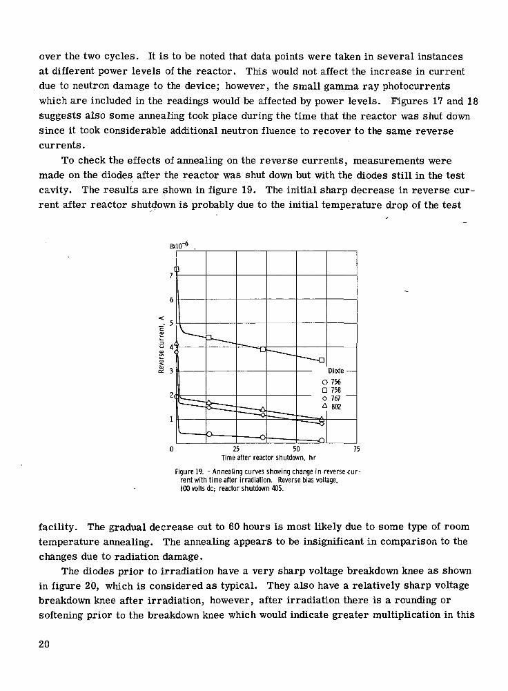
To check the effects of annealing on the reverse currents, measurements weremade on the diodes after the reactor was shut down but with the diodes still in the testcavity. The results are shown in figure 19. The initial sharp decrease in reverse cur-rent after reactor shutdown is probably due to the initial temperature drop of the test
8xlO"6
(
3 41<D i
g3. 3
2<
1
0 25 50Time after reactor shutdown, hr
75
Figure 19. - Annealing curves showing change in reverse cur-rent with time after irradiation. Reverse bias voltage,100 volts dc; reactor shutdown 40S.
facility. The gradual decrease out to 60 hours is most likely due to some type of roomtemperature annealing. The annealing appears to be insignificant in comparison to thechanges due to radiation damage.
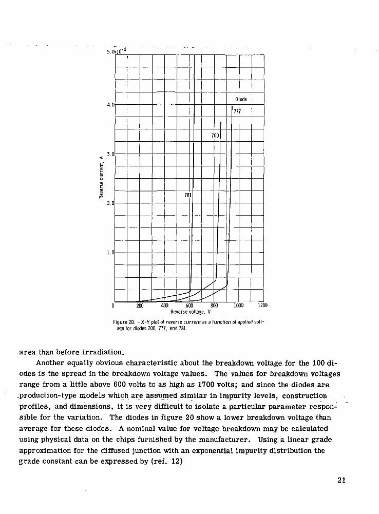
The diodes prior to irradiation have a very sharp voltage breakdown knee as shownin figure 20, which is considered as typical. They also have a relatively sharp voltagebreakdown knee after irradiation, however, after irradiation there is a rounding orsoftening prior to the breakdown knee which would indicate greater multiplication in this
20
5.0x10⁻⁴
4.0
3.0
2.0
1.0
781
700
Diode
777
200 400 600 800Reverse voltage, V
1000 1200
Figure 20. - X-Y plot of reverse current as a function of applied volt-age for diodes 700, 777, and 781.
area than before irradiation.Another equally obvious characteristic about the breakdown voltage for the 100 di-
odes is the spread in the breakdown voltage values. The values for breakdown voltagesrange from a little above 600 volts to as high as 1700 volts; and since the diodes are
.production-type models which are assumed similar in impurity levels, constructionprofiles, and dimensions, it is very difficult to isolate a particular parameter respon-sible for the variation. The diodes in figure 20 show a lower breakdown voltage thanaverage for these diodes. A nominal value for voltage breakdown may be calculatedusing physical data on the chips furnished by the manufacturer. Using a linear gradeapproximation for the diffused junction with an exponential impurity distribution thegrade constant can be expressed by (ref. 12)
21
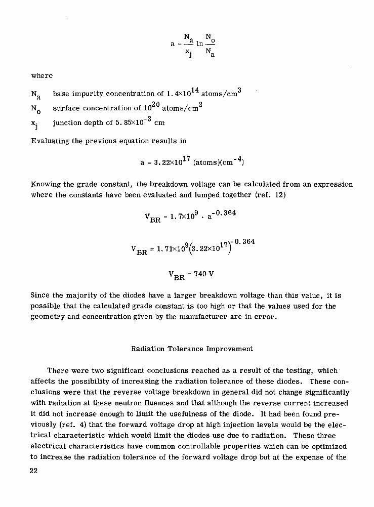
Na Noa = _§; In -2Xj Na
where
N0 base impurity concentration of 1.4x10 atoms/cma.
N surface concentration of 10 atoms/cm_3
x, junction depth of 5. 85x10 cmJ
Evaluating the previous equation results in
a = 3.22x10 (atoms)(cm~4)
Knowing the grade constant, the breakdown voltage can be calculated from an expressionwhere the constants have been evaluated and lumped together (ref. 12)
VBR = !-71xl09(3.22xl017)-0.364
VBR = 740 V
Since the majority of the diodes have a larger breakdown voltage than this value, it ispossible that the calculated grade constant is too high or that the values used for thegeometry and concentration given by the manufacturer are in error.
Radiation Tolerance Improvement
There were two significant conclusions reached as a result of the testing, whichaffects the possibility of increasing the radiation tolerance of these diodes. These con-clusions were that the reverse voltage breakdown in general did not change significantlywith radiation at these neutron fluences and that although the reverse current increasedit did not increase enough to limit the usefulness of the diode. It had been found pre-viously (ref. 4) that the forward voltage drop at high injection levels would be the elec-trical characteristic which would limit the diodes use due to radiation. These threeelectrical characteristics have common controllable properties which can be optimizedto increase the radiation tolerance of the forward voltage drop but at the expense of the
22
reverse current and breakdown voltages. These controllable parameters are the basethickness and base doping levels. Since the reverse breakdown voltages were in thegeneral range of 1200 to 1500 volts, and the specified breakdown voltage was 600 volts,the breakdown voltage could be reduced considerably and yet remain within specifica-
7 Rtions. The reverse current in the 600-volt bias range were in the 10" - to 10 -ampererange even after irradiation. This suggests that by decreasing the base width and in-creasing the base doping the following could be accomplished:
(1) There would be a decrease in reverse breakdown voltage but it would not affectthe useful lifetime because the breakdown voltage changes very little with radiation.
(2) A possible increase in surface leakage due to a shorter leakage path; however,there would be a lower generation-recombination bulk component due to the reducedvolume of the depletion region.
(3) A decrease in forward voltage drop because of the increased conductivity acrossthe base region and a smaller base thickness to diffusion length ratio (ref. 4). Thiswould extend the useful lifetime of the diode in a nuclear environment.
CONCLUSIONS
The reverse bias electrical characteristics of 100 high reliability silicon powerdiodes were investigated with respect to the effects of nuclear radiation on these char-acteristics. The conclusions were as follows:
1. The preirradiated diodes had very low reverse currents and sharp avalanchevoltage knees but there was considerable spread among the diodes in both reverse cur-rents and breakdown voltages.
2. The postirradiated diodes had:a. Large percentage changes in reverse currents but not enough increase to
limit the use of the diodes.b. Generally very little change in the breakdown voltages although there was
considerable softening or rounding of the knee.c. No appreciable change in the amount of spread in the reverse character-
istics.3. The preirradiated reverse current curves generally fell into two classes:
a. Normal curves where the current increased uniformly with increase inreverse bias. For these diodes the currents generally increased with radiation.
b. Irregular curves whose reverse currents increase unevenly with increasingbias. The current generally decreases with radiation for these diodes. Approxi-mately 30 percent of the diodes tested displayed this effect.4. A theoretical curve was calculated along with an estimate of change in the re-
verse characteristics due to irradiation and compared to experimental values. Only fair
23
agreement was found at lower voltage up to approximately 100 volts. Calculations athigher voltages were not possible due to the irregular experimental curves.
5. The effects of irradiating the diodes at different temperatures and operatingmodes were not discernable due to the spread in experimental data.
6. Attempts to correlate the unusual changes such as decreases in currents withradiation with changes in junction capacitance and forward characteristics were unsuc-cessful.
7. The results of this test indicate how these diodes can be made more radiationtolerant by a trade-off of capabilities in the very low reverse currents and very highbreakdown voltages for improved forward electrical characteristics.
Lewis Research Center,National Aeronautics and Space Administration,
Cleveland, Ohio, June 25, 1973,502-25.
24
APPENDIX A
SYMBOLS
oA. area of junction, cm
a grade constantr\
D diffusion constant for electrons in silicon, cm /sec
reverse current, A
reverse average cu
diffusion current, A
I reverse average current, A
I generation- recombination current, A
K Boltzmann constant, eV/K
K damage constant for siliconsLR low level diffusion length for electrons in p-region, cm
_ QN acceptor dopant concentration in p-region, cm
aq
NU surface concentration, atoms/cm_ Q
n. intrinsic carrier concentration, cmo
n density of electrons in p-region under thermal equilibrium conditions, cm
q charge on electron, C
T temperature, K
V » applied voltage, V
VB built-in voltage at junction (diffusion potential), V
Vgjj reverse breakdown voltage, V
W depletion region width, cm
x. junction depth, cmn
(f> neutron fluence, neutrons/cm -Teff effective minority carrier life time, sec
T limiting lifetime for electrons in heavily doped p-region, sec
T limiting lifetime for holes in heavily doped n- region, sec
25
APPENDIX B
REVERSE CURRENT CALCULATIONS
The reverse applied voltages in the few tenths of a volt range are of little impor-tance generally as far as circuit application is concerned since the values of current areso small. The cur rent-voltage data in this region does, however, furnish useful infor-mation as to the validity of the analytical approach and the physical parameters used inthe calculations.
As in the forward bias diodes, the reverse currents are made up of three compo-nents, generation-recombination, diffusion, and surface. Unlike the forward current,however, as the reverse bias is increased the diffusion component becomes a small fac-tor while the generation-re combination becomes the dominant component. The surfacecomponent is less predictable but undoubtedly contributes at all values of reverse bias.The diffusion and generation-re combination components are calculable and can be addedfor comparison with experimental values.
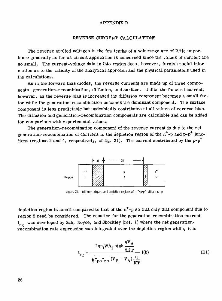
The generation-recombination component of the reverse current is due to the netgeneration-recombination of carriers in the depletion region of the n+-p and p-p+ junc-tions (regions 2 and 4, respectively, of fig. 21). The current contributed by the p-p+
--w-
Region
-2d-
Figure 21. - Different dopant and depletion regions of n+-p-p+ silicon chip.
depletion region is small compared to that of the n+-p so that only that component due toregion 2 need be considered. The equation for the generation-recombination currentI was developed by Sah, Noyce, and Shockley (ref. 1) where the net generation-recombination rate expression was integrated over the depletion region width; it is
• sinh2KT
rg f(b) (Bl)
26
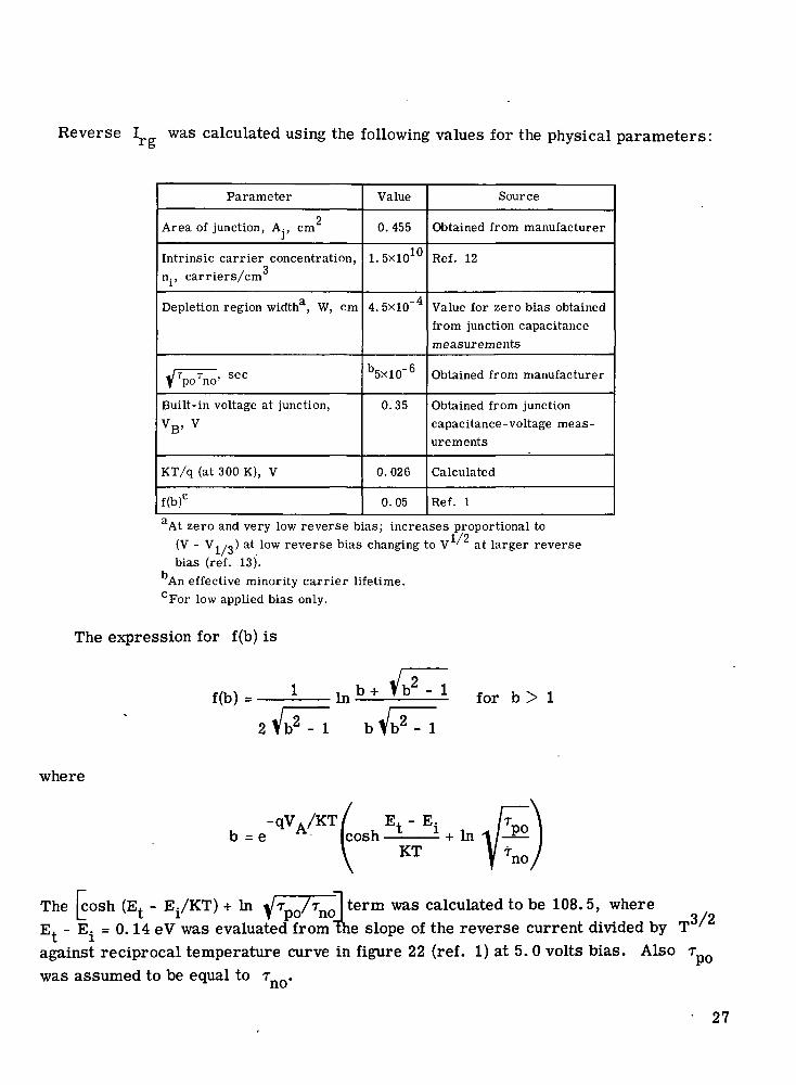
Reverse I was calculated using the following values for the physical parameters:
Parameter2
Area of junction, Aj, cm
Intrinsic carrier concentration,rip carriers/cm
Depletion region widtha, W, cm
VWno"' SGC
Built-in voltage at junction,VB, v
KT/q (at 300 K), V
f(b)C
Value
0.455
l.SxlO10
4. 5xlO"4
VlO'6
0.35
0.026
0.05
Source
Obtained from manufacturer
Ref. 12
Value for zero bias obtainedfrom junction capacitancemeasurements
Obtained from manufacturer
Obtained from junctioncapacitance-voltage meas-urements
Calculated
Ref. 1
At zero and very low reverse bias; increases proportional to1/2(V - Vj /g) at low reverse bias changing to V 'at larger reverse
bias (ref. 13).An effective minority carrier lifetime.For low applied bias only.
The expression for f(b) is
f(b) = 1 for b > 1
where
-qVA/KT/ E . - E .= e A cosh-i i + ln
V KT
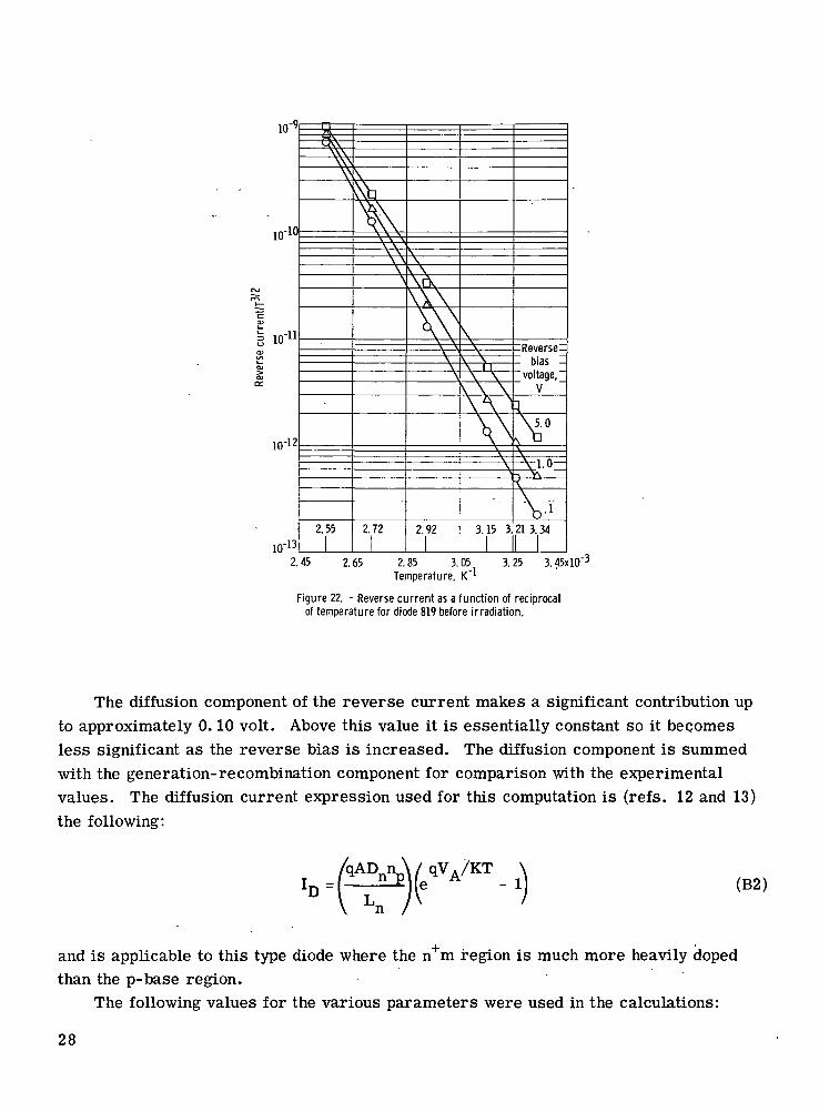
In term was calculated to be 108.5, where3/2
The [cosh (Et - E^Et ~ Ei = °'14 eV was evaluated from ^e slope of the reverse current divided by Tagainst reciprocal temperature curve in figure 22 (ref. 1) at 5. 0 volts bias. Also Twas assumed to be equal to TnQ.
27
Sa:
iin
10-io
-n
in-12
10-"
ft- —^-\\\v\\\\
\Nv
2.55
\
^h
\ \ >\ \\\\\\\
2.72
V\
^ \\r\
\\\
XV\\\\
2.92
\. \\ \\ n.\ \\\ \\^ ^\\\\\>
3.15 3.
Kjac
voltage,V
1
A
\ i n\ 1.0-\ \\\\
\).i21 3. 34
2.45 2.65 2.85 3.05 3.25 3.45x10Temperature, IO
Figure 22. - Reverse current as a function of reciprocalof temperature for diode 819 before irradiation.
,-3
The diffusion component of the reverse current makes a significant contribution upto approximately 0.10 volt. Above this value it is essentially constant so it becomesless significant as the reverse bias is increased. The diffusion component is summedwith the generation-recombination component for comparison with the experimentalvalues. The diffusion current expression used for this computation is (refs. 12 and 13)the following:
(B2)
and is applicable to this type diode where the n m region is much more heavily dopedthan the p-base region.
The following values for the various parameters were used in the calculations:
28
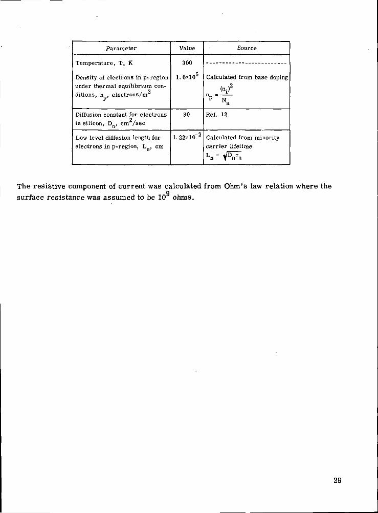
Parameter
Temperature, T, K
Density of electrons in p-regionunder thermal equilibrium con-
o
ditions, n , electrons/m
Diffusion constant for electronsn
in silicon, Dn, cm /sec
Low level diffusion length forelectrons in p-region, Ln, cm
Value
300
1.6X10⁶
30
1.22X10"2
Source
Calculated from base doping
Ref. 12
Calculated from minoritycarrier lifetime
The resistive component of current was calculated from Ohm's law relation where theQ
surface resistance was assumed to be 10 ohms.
29
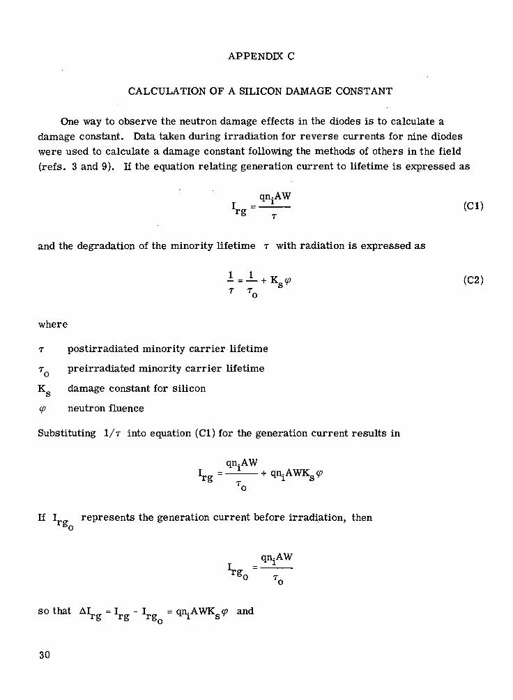
APPENDIX C
CALCULATION OF A SILICON DAMAGE CONSTANT
One way to observe the neutron damage effects in the diodes is to calculate adamage constant. Data taken during irradiation for reverse currents for nine diodeswere used to calculate a damage constant following the methods of others in the field(refs. 3 and 9). If the equation relating generation current to lifetime is expressed as
qn.AW
and the degradation of the minority lifetime T with radiation is expressed as
I = J - + K < p (C2)r To
where
T postirradiated minority carrier lifetime
T preirradiated minority carrier lifetime
K0 damage constant for siliconscp neutron fluence
Substituting 1/r into equation (Cl) for the generation current results in
qn.AWI r g= — - +qniAWKs<p
To
If I represents the generation current before irradiation, thens
qn.AW
so that AI^ = Irg - Irg = q n A W K ^ and
30
K =— -- ^ . . . (C3)S <p
Data from the first reactor cycles of tests I and II were used in determining the damageconstant K for silicon. These corresponded to cycles designated 39P and 41P, re-
O
spectively. The neutron fluence used was chosen from a portion of each cycle whichrepresented the least interruption of the flux due to shutdowns, start up or changingpower levels. Selections were based also on the fact that these particular cycles had aminimum of interruptions and the diodes had been exposed to a minimum of neutron fluxoscillations unlike the later cycles 40P and 42P. The change in reverse current withflux varies considerably among the diodes so that the calculated damage constants alsohave considerable variations. Due to this variation, the average change in reverse cur-rent of nine diodes was used in the calculations for the damage constant for each test.The reverse currents were taken at 100 volts reverse bias and although the operatingtemperature for cycle 41P was 125 C, the measurements were taken when the diodestemperatures were stabilized at around 28° C.
Values for K were calculated using the following:
q = 1.6X10"19
nt = 1.5X10¹⁰
A = 0. 455 cm2
W = 4. OxlO"3 cm
V =1. OxlO13 neutrons/cm2 (cycle 39P)
<p = 1.34X10¹³ neutrons/cm2 (cycle 41P)
AIaye = 1.6X10"6 A (cycle 39P)
AIave = °-95xlO"6 A (cycle 41P)
The values for Kc were 3. 6xlO"8 cm2 neutron"1 sec"1 for cycle 39P and 1. 6xlO~8 cm2
-1 -1neutron sec for cycle 41P. These values are in general agreement with damageconstants found by others (ref. 3). However, the damage constant for cycle 41P couldbe lower due to the annealing effects of the higher operating temperatures during thatcycle. Using these damage constants and the preirradiated lifetimes for the minority
31
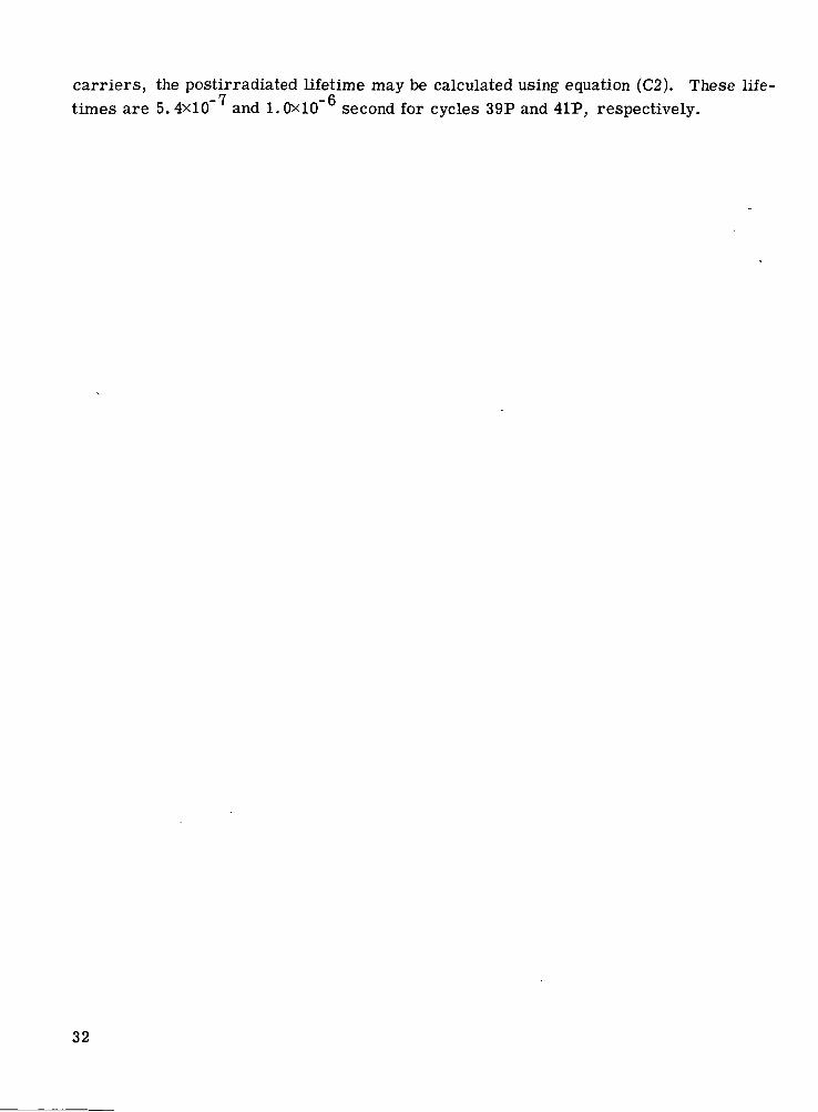
carriers, the postirradiated lifetime may be calculated using equation (C2). These life-7 R
times are 5.4x10" and 1.0x10" second for cycles 39P and 41P, respectively.
32
REFERENCES
1. Sah, Chih-Tang; Noyce, Robert N.; and Shockley, William: Carrier Generation andRecombination in P-N Junctions and P-N Junction Characteristics. Proc. IRE,vol. 45, no. 9, Sept. 1957, pp. 1228-1243.
2. Sah, Chih-Tang: Effects of Electrons and Holes on the Transition Layer Character-istics of Linearly Graded P-N Junctions. Proc. IRE, vol. 49, no. 3, Mar. 1961,pp. 613-618.
3. Larin, Frank: Radiation Effects in Semiconductor Devices. John Wiley & Sons,Inc., 1968.
4. Been, Julian F.: Effects of Nuclear Radiation on a High-Re liability Silicon PowerDiode, n - Analysis of Forward Electrical Characteristics. NASA TN D-5732,1970.
5. Anon.: Screening Specifications for Semiconductor Device SIN1189. NASA MarshallSpace Flight Center, Apr. 1963.
6. Davies, R. L.; and Gentry, F. E.: Control of Electric Field at the Surface of P-NJunctions. IEEE Trans, of Electron Devices, vol. ED-11, no. 7, July 1964,pp. 313-323.
7. Bozek, John M.; and Godlewski, Michael P.: Experimental Determination of Neu-tron Fluxes in Plum Brook Reactor HB-6 Facility with Use of Sulfur Pellets andGold Foils. NASA TM X-1497, 1968.
8. Bozek, John M.: Experimental Determination of Gamma Exposure Rate in PlumBrook HB-6 Facility. NASA TM X-1490, 1968.
9. Frank, Max; and Taulbee, Carl D.: Handbook for Predicting Semiconductor DevicePerformance in Neutron Radiation. Bendix Corp., Mar. 1967. (ContractAF29(601)-7110).
10. Messenger, George C.; et al.: Device Performance Characteristics as Related toRadiation Damage in Semiconductor Materials. Rep. ARD-66-42-R, NorthropCorp. (AFCRL-66-462, DDC No. AD-643703), June 1966.
11. Batdorf, R. L.; Chynoweth, A. G.; Dacey, G. C.; and Foy, P. W.: UniformSilicon P-N Junctions. I. Broad Area Breakdown. J. Appl. Phys., vol. 31,no. 7, July 1960, pp. 1153-1160.
12. Phillips, Alvin B.: Transistor Engineering and Introduction to Integrated Semicon-ductor Circuits. McGraw-Hill Book Co., Inc., 1962.
13. Lindmayer, Joseph; and Wrigley, Charles Y.: Fundamentals of Semiconductor De-vices. D. Van Nostrand Co., Inc., 1965.
NASA-Langley, 1973 24 E-7362 33
NATIONAL AERONAUTICS AND SPACE ADMINISTRATION
WASHINGTON. D.C. 2O546
OFFICIAL BUSINESS
PENALTY FOR PRIVATE USE $3OO SPECIAL FOURTH-CLASS RATEBOOK
POSTAGE AND FEES PAIDNATIONAL AERONAUTICS AND
SPACE ADMINISTRATION431
POSTMASTER : If Undeliverable (Section 158Postal Manual) Do Not Return
"The aeronautical and space activities of the United States shall beconducted so as to contribute . . . to the expansion of human knowl-edge of phenomena in the atmosphere and space. The Administrationshall provide for the widest practicable and appropriate disseminationof information concerning its activities and the results thereof."
—NATIONAL AERONAUTICS AND SPACE ACT OF 1958
NASA SCIENTIFIC AND TECHNICAL PUBLICATIONSTECHNICAL REPORTS: Scientific andtechnical information considered important,complete, and a lasting contribution to existingknowledge.
TECHNICAL NOTES: Information less broadin scope but nevertheless of importance as acontribution to existing knowledge.
TECHNICAL MEMORANDUMS:Information receiving limited distributionbecause of preliminary data, security classifica-tion, or other reasons. Also includes conferenceproceedings with either limited or unlimiteddistribution.
CONTRACTOR REPORTS: Scientific andtechnical information generated under a NASAcontract or grant and considered an importantcontribution to existing knowledge.
TECHNICAL TRANSLATIONS: Informationpublished in a foreign language consideredto merit NASA distribution in English.
SPECIAL PUBLICATIONS: Informationderived from or of value to NASA activities.Publications include final reports of major 'projects, monographs, data compilations,handbooks, sourcebooks, and specialbibliographies.
TECHNOLOGY UTILIZATIONPUBLICATIONS: Information on technologyused by NASA that may be of particularinterest in commercial and other non-aerospaceapplications. Publications include Tech Briefs,Technology Utilization Reports andTechnology Surveys.
Details on the ava/fabi//ty of fhese pubf/cafions may be obtained from:
SCIENTIFIC AND TECHNICAL INFORMATION OFFICE
N A T I O N A L A E R O N A U T I C S A N D S P A C E A D M I N I S T R A T I O N
Washington, D.C. 20546


![Radiation Effects in Graphite - Indico [Home]indico.ictp.it/event/7633/session/1/contribution/17/... · 2016-09-08 · Radiation Effects in Graphite Michael I. Ojovan Nuclear Engineer,](https://img.pdfslide.net/doc/110x75/5e34c2ac3d88dc6fdd166bd3/radiation-effects-in-graphite-indico-home-2016-09-08-radiation-effects-in.jpg)