Embed Size (px)
Citation preview

Effects of Solder Mask on Electrochemical Migration of Tin-Lead and Lead-Free Boards
Xiaofei He1, Michael H. Azarian1, Michael G. Pecht1,2
1Center for Advanced Life Cycle Engineering (CALCE) University of Maryland
College Park, MD 20742 USA Phone: +1-301-405-5323, FAX: +1-301-314-9269
2Prognostics and Health Management Center City University of Hong Kong, Kowloon, Hong Kong
Abstract
Electrochemical migration (ECM) is the growth of conductive metal filaments on a printed circuit board (PCB) through an electrolyte solution under a DC voltage bias. ECM can cause a reduction in surface insulation resistance (SIR) between adjacent conductors, generate a path of leakage current, and lead to intermittent or catastrophic circuit failures.
Solder mask has been widely used on printed circuit boards to define wettable surfaces, reduce moisture access, control outer layer impedance, and improve corrosion resistance. The mechanical and thermal properties of solder mask have been widely reported, but systematic studies of their influence on ECM have been few. This paper presents the results of temperature-humidity-bias (THB) testing of more than 1000 hours duration at 40V, 65˚C, and 88% relative humidity for comparative evaluation of ECM on circuit boards with and without a solder mask. The boards were HASL finished and wave soldered using a no-clean, low solids flux. Besides primarily assessing the effects of using a solder mask on ECM, the effects of solder alloy composition (eutectic SnPb versus Sn-3.0Ag-0.5Cu) were also investigated. In situ monitoring of SIR was performed throughout these tests. Optical microscopy and scanning electron microscopy were employed to examine the correlation between the physical attributes of dendrites and the measured SIR, as well as to evaluate the effects of solder mask and solder alloy on ECM. Ion chromatography (IC) was conducted to measure contaminant levels on the surface of the PCBs. Elemental mapping by energy dispersive X-ray spectroscopy was employed to identify the migrating species and their distributions and morphologies within the dendrites. As expected, the use of a solder mask resulted in higher SIR, but a dramatic difference was observed in its effect on dendritic growth and characteristic life.
1. Introduction Electrochemical migration (ECM) is a failure mechanism that is manifested as a reduction in surface insulation resistance (SIR) of a printed circuit board (PCB). These failures can be either intermittent or permanent, depending on the morphology of the resulting dendrites and the current density. The occurrence of ECM requires an electrolyte, a voltage bias, and migrating metal. The electrolyte comprises dissolved ions and a solvent. The solvent can be either condensed water or non-condensed moisture adsorbed onto the substrate. Moisture adsorption is likely to be encountered in field usage. For the electrolyte to be able to dissolve contaminants and transport ions at least three monolayers of adsorbed moisture are required [1]. Twenty monolayers of adsorption can make the electrolyte sufficiently thick to transport ions easily [2]. The voltage bias between metallization on the board acts as a driving force for ion migration. The migrating metal may come from metallization (copper traces), surface finishes (such as immersion tin, silver, etc.), or solder (such as SnPb, SnAgCu, etc.). The ECM process consists of the following sequence of steps: path formation, electrodissolution, ion transport, electrodeposition, and dendrite growth [3]. Path formation is the formation of a preferential path including an electrolyte layer through which metal ions migrate. This step depends on the PCB material composition, board surface roughness, concentration and distribution of contaminants, and environmental conditions. For example, in a temperature range of 40ºC~85ºC polyimide (PI) was found to absorb about twice as much moisture as that absorbed by FR-4, cyanate ester (CT) and bismaleimide triazine (BT) laminates, which have similar moisture absorption [4]. Pores, scratches, and cavities on the surface, which have higher surface energy than a smooth surface, tend to adsorb thicker water layers from the environmental humidity. The existence of contamination such as flux residues and fibers further enhances the adsorption of moisture. Relevant environmental conditions include temperature, humidity, and airborne contaminants [3]. Electrodissolution involves the solvation of metals to become cations at the anode (positive electrode) through oxidation. Under a DC bias voltage metal cations migrate to the cathode (the ion transport step), get reduced into neutral metal, and deposit onto the cathode (electrodeposition). As more and more metal deposits on the cathode, a dendritic structure grows from the cathode toward the anode.
As originally published in the IPC Printed Circuit Expo, APEX & Designer Summit Proceedings.

A solder mask is a thin, heat-resistant polymeric layer commonly applied to PCBs to define the wettable regions during the soldering process [5]. It prevents solder from being deposited onto undesired areas such as the area between copper metallization traces. It controls outer layer impedance and protects PCBs from handling damage during assembly. The material composing a solder mask can be polyimide [5] or modified epoxy [6]. Polyimide and epoxy resin are both thermosets [7]—they readily cross-link during curing and form a rigid network. The properties of solder mask and their influence on PCBs have received some attention in the literature. For example, the connection between solder mask and the thermal fatigue life of solder joints was reported by Michaelides, et al. [8]. The temperature dependence of the mechanical behavior of a solder mask can be found in the work of Darveaux, et al. [9]. An FEM model was built to analyze the warpage of solder mask by Ume, et al. [6]. Zhu, et al [5] investigated the stiffness and creeping properties of a polyimide solder mask. A difference in properties between temporary and permanent solder mask was reported by Cheng [10]. However, there have been few published assessments on the effect of solder mask on ECM, especially when no-clean processes were used. In order to address the effect of a solder mask on ECM, together with the effects of solder alloys, a comparative experiment was designed and performed. 2. Experimental Setup Table 1 presents the test matrix. The pairs of comparisons include: solder mask versus no solder mask, and eutectic Sn-37Pb versus Sn-3.0Ag-0.5Cu (SAC305) solder (matched with the appropriate HASL finish). All the samples experienced wave soldering using a no-clean low solids flux (ROL0). Low solids refers to a solids content of less than 4%. For each combination of solder mask and solder 3 identical samples were used, so in total there were 12 samples. The test vehicles in this experiment were modified IPC-B-24 patterns with FR-4 as the substrate, as shown in Figure 1. The difference was that IPC-B-24 patterns have 16 mil and 20 mil spacings, while the test vehicle in the current study had 25 mil spacings. On boards with solder mask, the solder mask was applied over the end of the comb pattern, in between the comb fingers, and to the rest of the PCB.
Table 1 Test Matrix for 4 Boards Processed with Different Factors Solder Process Flux* Finish Solder Mask**
Eutectic SnPb Wave ROL0 low solids SnPb HASL SM Eutectic SnPb Wave ROL0 low solids SnPb HASL No SM
SAC305 Wave ROL0 low solids LF_HASL SM SAC305 Wave ROL0 low solids LF_HASL No SM
* “ROL0” means the flux contains rosin, has a low activity, and a halide content of less than 0.05%. ** “SM” means that the board had a solder mask, and “No SM” means that there was no solder mask.
Figure 1: Modified IPC-B-24 samples of 25 mil spacings with (left) and without (right) a solder mask A surface insulation resistance (SIR) test system was used on the PCB boards in this study to detect leakage current. SIR represents both surface and bulk conduction resistance, but when conductive filament formation does not occur, 99.9% of the leakage current takes a surface path [11]. Our SIR test system comprised a computer, a high resistance meter, four low-noise matrix switches, a temperature-humidity chamber, a DC power supply, and test boards. The 4-channel high resistance meter was an Agilent 4349B with a measurement range from 103 Ohms to 1015 Ohms. Its accuracy ranges from 2.5%~3.1%. The matrix switches were Agilent and HP E5252A, capable of multiplexing 48 channels of low current data.
As originally published in the IPC Printed Circuit Expo, APEX & Designer Summit Proceedings.

The SIR value of each test sample was collected once every 3.6 minutes in order to stabilize the data acquisition. A 1-MOhm resistor was located in series with each SIR test structure to limit the current. This resistor was chosen to minimize the chances that dendrites would fuse open due to high current density while allowing the current to change appreciably even if the test resistance went below the failure threshold. The temperature and humidity conditions (65°C/88%RH) were selected based on the recommendations of industrial standard IPC-TM-650 method 2.6.14.1. In order to track the SIR evolution of the test samples, a total test time of around 1400 hours was used. The bias voltage was 40V DC. The SIR failure threshold was 100 MOhms, which was consistent with the criteria cited in IPC J-STD-004A method 3.4.5.1 and IPC-9201. 3. Results and Discussion 3.1 Solder Mask vs No Solder Mask: SIR This test was composed of four boards with the processing factors specified in Table 1. There were 2 corresponding pairs for comparing the use and non-use of solder mask. As shown in Table 2, the samples with solder mask all survived the THB test, but samples without solder mask all failed within 110 hours, regardless of whether SnPb or SAC solder was used. SAC soldered samples failed consistently earlier than SnPb soldered samples.
Table 2 Test Matrix and Failure Pattern for 4 Boards Processed with Different Factors
Solder Finish Solder Mask
SIR Failure Times (hours)* Dendritic Growth
Sample 1 Sample 2 Sample 3
SnPb SnPb HASL
SM s s s None
No SM 106 49 36 Extensive
SAC SAC HASL
SM s s s 1 place
No SM 15 16.2 11.5 Extensive *Note; “s” means the sample survived the test and did not fail, “SM” means that the sample had a solder mask, and “No
SM” means that no solder mask was present. The boards with solder mask showed consistently higher SIR by one or two orders of magnitude than those without solder mask for the entire test. After an equilibrium period of 150 hours, the SIR of the SnPb soldered boards with solder mask stabilized at around 2×10⁹ Ohms, but the SIR of the SnPb soldered boards without solder mask oscillated at around 107 Ohms for the rest of the test, as shown in Figures 2 and 3. Similarly, the SIR of the SAC soldered boards with solder mask stabilized around 109 Ohms, but the SIR of the SAC soldered boards without solder mask oscillated between 107 and 108 Ohms, as shown in Figures 4 and 5. Thus, the solder mask coated boards had relatively stable SIR curves after a stabilization period, but the boards without solder mask had more intermittent SIR drops throughout the test. 3.2 Solder Mask vs No Solder Mask: ECM The most significant observation was the failure of all boards without solder mask, regardless of whether SnPb or SAC solder was used. All the samples on this type of assembly using either SnPb or SAC solder failed before 110 hours, although SAC soldered samples failed consistently earlier than SnPb soldered samples. Dendrites spanned the gap on all the failed samples, as shown in Figures 6 and 7. On boards with solder mask, dendrites rarely emerged, but between the edges of the solder mask and the copper traces, white deposits occurred in some places and were confined in these areas, as shown in Figure 8.
As originally published in the IPC Printed Circuit Expo, APEX & Designer Summit Proceedings.
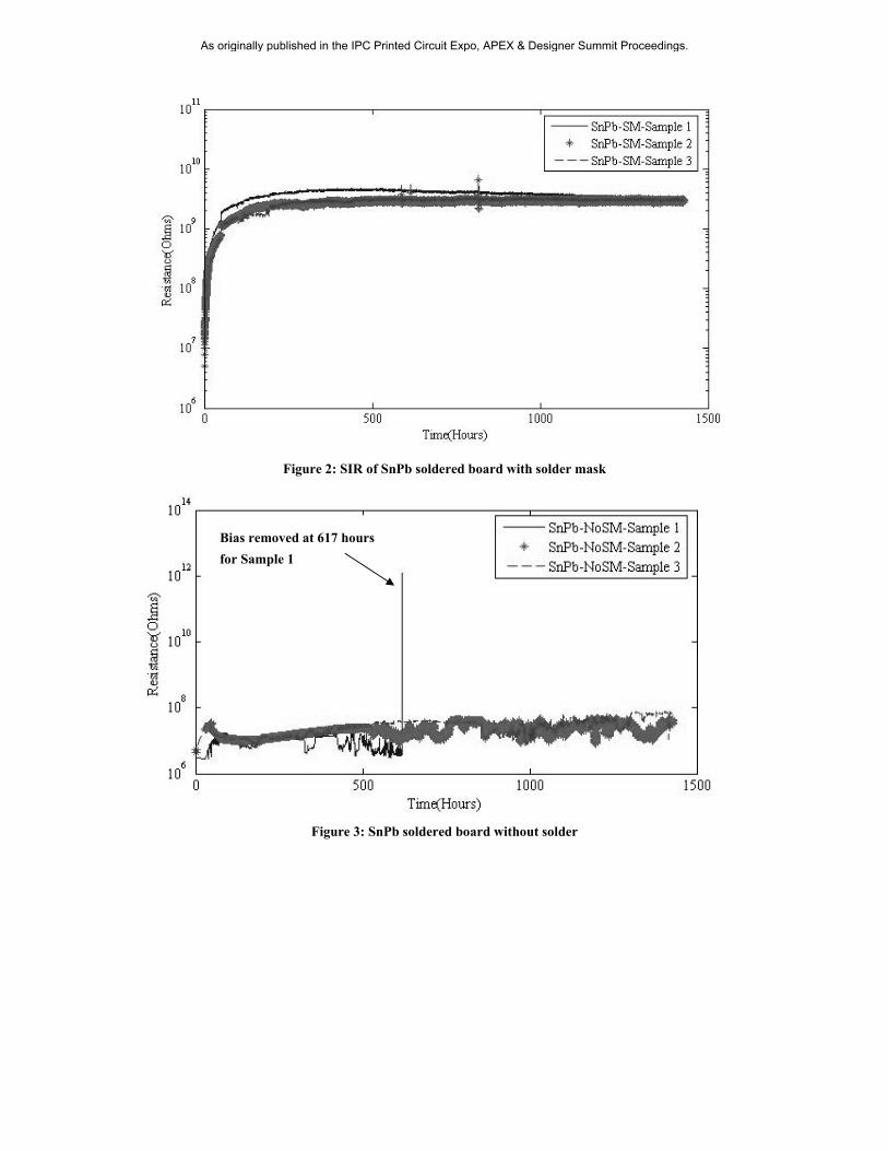
Figure 2: SIR of SnPb soldered board with solder mask
Figure 3: SnPb soldered board without solder
Bias removed at 617 hours for Sample 1
As originally published in the IPC Printed Circuit Expo, APEX & Designer Summit Proceedings.

Figure 4: SAC soldered board with solder mask
Figure 5: SAC soldered board without solder mask
Solder mask-coated boards exhibited little dendritic growth and higher (around 109 Ohms) and relatively stable SIR, but bare FR-4 boards displayed extensive dendritic growth and lower (around 107 Ohms) and oscillating SIR. This phenomenon indicates a correlation between dendritic growth and SIR. Once dendrites start to grow they help lower the SIR due to their conductive nature and keep SIR at this lower level. During their growth, dendrites can break due to burn-out [12] or mechanical stress [13], but quick regrowth is observable [13]. This breaking and regrowth may cause the SIR to oscillate in a cyclic fashion. On the other hand, it seems that without typical dendrites on solder mask-coated boards, the deposits confined between the edges of the solder mask and the copper traces could not influence the SIR very much.
Bias removed at 617 hours for Sample 3
As originally published in the IPC Printed Circuit Expo, APEX & Designer Summit Proceedings.

Figure 6: Optical micrograph of a failed sample on the SnPb soldered board without solder mask
Figure 7: Optical micrograph of a failed sample on the SAC soldered board without solder mask
+
+
-
+
-
As originally published in the IPC Printed Circuit Expo, APEX & Designer Summit Proceedings.

Figure 8: Optical micrograph of a survived sample on the SnPb soldered board with solder mask
Another reason why the use of a solder mask enhances SIR may be attributed to the material that a solder mask is composed of. Typical solder mask materials include photo-definable epoxy acrylate blends in dry film and liquid forms [14], which have attractive features such as high chemical resistance, high heat resistance, and high moisture resistance. When there is no solder mask, the flux sticking to the edge of copper traces effectively reduces the non-conductive spacing. With a shrunken gap between conductors, some weak organic acids inside the flux, such as glutaric acid and adipic acid [3], are more likely to build up a continuous conductive leakage path due to their hydrophilic nature and lower SIRs.
In places where there were dendrites, white residues were often present and spanned the gap, either by mixing with the dendrites or as a thin layer covering the dendrites. The correspondence in shape before and after THB exposure, as shown in Figure 9, clearly reveals the origin of these white residues to be flux residues.
(a) (b)
Figure 9: Optical micrographs of a failed sample on the SnPb soldered board without solder mask (a) before THB test, and (b) after THB test
EDS mapping of the elemental composition of the white residue revealed that Sn was its major constituent. On the SnPb assembly, the migrated species in the gap included Sn, Pb, and Cu, among which Sn was the most prevalent element, Pb
+
-
+
-
-
Solder Mask
+
+
As originally published in the IPC Printed Circuit Expo, APEX & Designer Summit Proceedings.

was comparable but less than Sn, and Cu occupied only a small proportion. On the SAC assembly Sn, Cu and Ag all migrated, among which Sn and Cu made up large proportions, while only a small amount of Ag migrated. Pb and Cu manifested themselves as dendrites (Figures 11 and 12), but Sn appeared as a layer spreading across the gap, but not in the form of typical dendrites, as shown in Figures 10 and 12. 3.3 Solder Mask vs No Solder Mask: Contamination Level An ion chromatography (IC) test was performed to characterize the contamination level on the boards. IC is a method used to separate and analyze mixtures of materials, either cations or anions, based on their ionic properties and their interaction with the sorbents in a packed bed column. The IC system used in this work, a DIONEX-600 System, is a type of liquid ion-exchange chromatography, which exploits ionic interaction and competition to separate analytes. The current work involves anion separation. The retention times of different peaks can be used to identify the ions, and the areas below the peaks are used to determine their concentrations. Figures 13 and 14 are the ion chromatograms for the SnPb soldered board without solder mask and the SAC soldered board without solder mask, respectively. The contaminant levels were calculated with respect to a control, which was analyzed using the same extraction and IC procedure but without any board. Table 4 gives the maximum acceptable contamination levels for chloride and bromide recommended by the National Defense Center for Environmental Excellence [15] and IPC [16]. IPC recommends a 1.56 µg/cm2 NaCl equivalent as a threshold for ionizable surface contaminations, but this standard considers the overall conductivity of both cations and anions, so it cannot be applied directly to anions, which is the output of IC and the most relevant category of contaminant ions for ECM. The comparison of anionic contaminants analyzed by IC with the acceptance levels requires conversion of the NaCl equivalent to halide equivalent (considering only anions). The amount of sodium ions can be converted to the amount of chloride or bromide which creates the same conductivity by assuming infinite dilution and using limiting ionic conductivity. Although infinite dilution is rarely encountered in practical situations, it is still a meaningful approximation because when an ion concentration is less than 10-3 mol/L (the so called Debye-Huckel region), it starts to behave as it would in infinite dilution [17]. Referring to Table 3 for chloride and bromide, 1.56 µg/cm2 NaCl equals
22114
21142 /57.1
/)5.3523(/5.35/56.1/5.35
104.761011.50
/231
/)5.3523(/23 /56.1 cmg
molgmolgmolgmolg
mmolohmmmolohm
molgmolgmolgcmg μμ =
+⋅+⋅
××
⋅⋅+
⋅ −−−
−−−
of equivalent Cl- and similarly 3.43 µg/cm2 of equivalent Br-. After this conversion, 1.56 µg/cm2 NaCl can be considered as 1.57 µg/cm2 chloride only or 3.43 µg/cm2 bromide only (Table 4), which are higher than the recommended levels by NDCEE. From the comparison between Tables 4, it can be seen that NDCEE places a lower threshold on the maximum acceptable contamination levels, but the experimental results (Table 5) in this study do not support its criteria. The adjusted IPC criteria, however, have more support in the experimental results, since the actual chloride level is still well below the chloride threshold (1.57 µg/cm2) and both of the two failed boards exceeded the bromide threshold (3.43 µg/cm2), although the actual bromide level on the survived SAC soldered board with solder mask also exceeded the bromide threshold. This may be due to the presence of solder mask. Without using solder mask, the two boards whose actual bromide levels exceeded the adjusted IPC criteria readily failed. In the presence of the solder mask, even if the actual bromide level exceeded the acceptance criteria by 11%, the elevated risk still does not produce a failure. It can also be observed that in this work bromide predominated over chloride in determining the risk of failure of the boards. Low levels of fluoride and sulfate were also present, but they seem to have played a secondary role compared to the larger concentration of bromide.
Table 3 Limiting Ionic Conductivity and Molecular Weight for Three Types of Anions Cl- Br- Na+ Limiting ionic conductivity (10-4ohm-1mol-1m2)
76.4 78.4 50.11
Molecular weight 35.5 79.9 23
Table 4 Maximum Acceptable Contamination Level for PCBs (µg/cm2)
* For no-clean flux.
** based on the IPC/EIA J-STD-001C recommendation of 1.56 µg/cm2 NaCl equivalent ionic residues as the maximum contamination level for PCBs.
NDCEE [15]* Based on IPC [16]**
Cl- 0.39 1.57 Br- 2.33 3.43
As originally published in the IPC Printed Circuit Expo, APEX & Designer Summit Proceedings.

Figure 10: SEM/EDS analysis of a failed sample on the SnPb soldered board without solder mask. There was a close correspondence in shape between the backscattered electron (BSE) image on the left and the Sn map (right image). Sn appeared to be a layer spread across the gap.
BSE Sn
_
+
As originally published in the IPC Printed Circuit Expo, APEX & Designer Summit Proceedings.

Figure 11: SEM/EDS analysis of a failed sample on the SnPb soldered board without solder mask. In the BSE
image (on the left), the brighter dendritic metal was Pb (see EDS map on the right), and the duller regions contained a distribution of Sn.
BSE
_
+
_
As originally published in the IPC Printed Circuit Expo, APEX & Designer Summit Proceedings.

BSE O
_
+
Figure 12: SEM/EDS analysis of a failed sample on the SAC soldered board without solder mask. Notice the similarity in shape between the bright feature in the BSE image, and the Cu and O maps. Migrated Cu appeared to be dendrites and may have been oxidized after the test. Migrated Sn appeared in a disperse layer spread across the gap.
As originally published in the IPC Printed Circuit Expo, APEX & Designer Summit Proceedings.

Sn Cu
As originally published in the IPC Printed Circuit Expo, APEX & Designer Summit Proceedings.

0.00 0.50 1.00 1.50 2.00 2.50 3.00 3.50 4.00 4.50 5.00 5.50 6.00 6.50 7.00 7.50 8.00-0.50
0.00
1.00
2.00
2.50 ECM_solder mask_40V_Xiaofei #19 [modified by Default, 2 peaks Sample 3 ECD_µS
min
1 - 1.808
2 - Chloride - 2.208
3 - Bromide - 3.050
Figure 13: Ion chromatogram of the SnPb soldered board without solder mask
0.00 0.50 1.00 1.50 2.00 2.50 3.00 3.50 4.00 4.50 5.00 5.50 6.00 6.50 7.00 7.50 8.00-0.20
0.50
1.00
1.50
2.00 ECM_solder mask_40V_Xiaofei #7 [modified by Default, 3 peaks Sample 2 ECD_µS
min
1 - 1.833
2 - Chloride - 2.217
3 - Bromide - 3.108
4 - Sulfate - 4.550
Figure 14: Ion chromatogram of the SAC soldered board without solder mask
Table 5 Actual Contamination Levels for the 4 Boards Processed with Different Factors, plus the Control 4. Conclusions Solder mask was found to enhance the SIR of PCBs, lower the chances of ECM failures, and reduce the susceptibility to ECM. In this study solder mask increased SIR by one or two orders of magnitude, regardless of whether SnPb or SAC solder was used. Solder mask also resulted in a relatively stable SIR over an extended period of more than 1400 hours, while bare FR-4 boards showed a fluctuating SIR throughout the test. The high and stable SIRs manifested by solder mask coated boards were attributed to the lack of dendritic growth, the material composition of the solder mask, and the confining effect between the walls of the solder mask and the copper traces of any small dendrites that grew in that area. The relatively low and varying SIRs of bare FR-4 boards were due to the extensive dendritic growth and metal migration between the copper traces.
Solder Finish Solder Mask
Amount (µg/cm2) Fluoride Chloride Bromide Nitrate Sulfate
SnPb SnPb HASL
SM 0.12 0.50 1.41 / / NoSM / 0.13 5.67 / /
SAC SAC HASL
SM 0.41 0.53 3.82 / 0.36 NoSM / 0.13 4.66 / 0.24
Control 0.34 / / 3.07 /
As originally published in the IPC Printed Circuit Expo, APEX & Designer Summit Proceedings.

Flux residues were found to become white deposits after THB exposure. White residues always co-existed with dendrites, mixed with or covering the dendrites. The white residue contained relatively large amounts of Sn which did not exhibit a dendritic morphology but rather was present as a dispersed layer. Migrated metal on SnPb soldered boards contained Sn, Pb and Cu, while migrated metal on SAC soldered boards contained Sn, Cu and Ag. Lead, copper, and silver manifested themselves as dendrites in contrast to tin’s migration as layers or fine particles. Bare FR-4 boards were found to contain higher levels of extractable bromide than solder mask-coated boards. This may have contributed to the extensive dendritic growth on the boards. A method to calculate the acceptance limit of ionic contaminants based on IPC J-STD-001C was presented. The principle is to maintain the conductivity the same and use limiting ionic conductivity to calculate the concentrations of different types of ions. In light of this adjusted contamination threshold (1.57 µg/cm2 for chloride only, or 3.43 µg/cm2 for bromide only), the bromide on the failed bare FR-4 boards already exceeded the threshold. One solder mask-coated board did not exceed either the chloride or the bromide threshold and, thus, survived. Another solder mask coated board slightly exceeded the bromide threshold but still survived, demonstrating the solder mask’s role in lowering the susceptibility to ECM.
Acknowledgements This research was supported by the members of the CALCE Electronic Products and Systems Consortium at the University of Maryland, College Park. References
[1] G. Cvijanovich, “Conductivities and Electrolytic Properties of Absorbed Layers of Water,” Proc. of NBS/RADC
Works., Moist. Meas. Tech. for Herm. Semic. Devi, II, Maryland, pp. 149, 1980. [2] M. Zamanzadeh, S. Meilink, G. Warren, P. Wynblatt, B. Yan, “Electrochemical Examination of Dendritic
Growth on Electronic Devices in HCl Electrolytes,” Corrosion, Vol. 46, No. 8, pp. 665-671, 1990. [3] S. Zhan, M. H. Azarian and M. Pecht, “Surface Insulation Resistance of Conformally Coated Printed Circuits
Boards Processed with No-Clean Flux,” IEEE Trans. Electr. Packag. Manufac., Vol. 29, No. 3, pp. 217-223, July 2006.
[4] M. Pecht, H. Ardebili, A. Shukla, J. Hagge and D. Jennings, “Moisture Ingress into Organic Laminates,” IEEE Trans. Compo. Packag. Tech, Vol.22, No. 1, pp. 104-110, 1999.
[5] H. Zhu, Y. Guo, W. Li, A. Tseng, and B. Martin, “Micro-Mechanical Characterization of Solder Mask Materials,” IEEE, Electr. Packag. Tech. Conf., pp. 148-153, 2000.
[6] I. C. Ume, T. Martin, and J. T. Gatro, “Finite Element Analysis of PWB Warpage Due to the Solder Masking Process,” IEEE Trans. Compo. Packag. Manufac. Tech., A, Vol. 20, No. 3, pp. 295-306, 1997.
[7] F. L. Matthews, and R. D. Rawlings, Composite Materials: Engineering and Science, CRC Press LLC, Boca Raton, 1999.
[8] S. Michaelides and S. K. Sitaraman, “Effect of Materials and Geometry Parameters on the Thermal-Mechanical Reliability of Flip-Chip Assemblies,” IEEE Therm. Mech. Pheno. Electr. Syst., pp. 193-200, 1998.
[9] R. Darveaux, L. Norton, and F. Carney, “Temperature Dependent Mechanical Behavior of Plastic Packaging Materials,” IEEE Proc. Electr. Compo. Tech. Conf., pp. 1054-1058, 1995.
[10] L. W. Cheng, “Application of Temporary Solder Mask in SMT of High Frequency Circuit Boards,” IEEE ICEPT, 5th Int’l Conf. Electr. Packag. Tech. Proc., pp. 467-470, 2003.
[11] D. Q. Yu, W. Jillek, E. Schmitt, “Electrochemical migration of Sn-Pb and lead free solder alloys under distilled water,” J Mater Sci: Mater Electron, Vol. 17, pp. 219–227, 2006.
[12] S. Zhan, M. H. Azarian and M. Pecht, “Reliability of Printed Circuit Boards Processed Using No-Clean Flux Technology in Temperature-Humidity-Bias Conditions,” IEEE Trans. Devi. Materi. Reliab., Vol. 8, No. 2, 2008.
[13] J. Bradley, H. Chen, J. Crawford, J. Eckert, K. Ernazarova, T. Kurzeja, M. Lin, M. McGee, W. Nadler, and S. Stephens, “Creating Electrical Contacts between Metal Particles Using Directed Electrochemical Growth,” Nature, Vol. 389, pp. 268-270, 1997.
[14] Petefish, William, George, “Dimensionally Stable Solder Mask Material and Method of Application,” WO/1998/020713, 1998.
[15] National Defense Center for Environmental Excellence (NDCEE), “Joint Test Protocol CC-P-1-1 for Validation of Alternatives to Lead-Containing Surface Finishes, for Development of Guidelines for Conformal Coating Usage, and for Qualification of Low-VOC Conformal Coatings,” Contract No. DAAA21-93-C-0046, Johnstown, PA, June 1999.
[16] IPC, “Requirements for Soldered Electrical and Electronic Assemblies,” J-STD-001C, Section 8.3.6, Northbrook, IL, March 2000.
[17] C. H. Hamann, A. Hamnett, and W. Vielstich, Electrochemistry, Wiley-VCH, New York, 1998.
+ -
As originally published in the IPC Printed Circuit Expo, APEX & Designer Summit Proceedings.


![Preparation of anodic aluminum oxide (AAO) nano-template …electrolytes under appropriate electrochemical conditions [3-5]. The synthesis and application of nanoporous alumina mask](https://img.pdfslide.net/doc/110x75/60c2ff62b7970f410e08e26b/preparation-of-anodic-aluminum-oxide-aao-nano-template-electrolytes-under-appropriate.jpg)