Embed Size (px)
Citation preview
Effects of Tin Mitigation Processes on Whisker Growth and Solder Joint Reliability for Chip and
Small-Outline Package Components
Tom Lesniewski
Northrop Grumman Network Communications Division San Diego, CA 92128

Topics• Study Overview
– Objectives and Test Plan– Variables and Components Covered– Pass/Fail Criteria
• Results & Discussion• Conclusions & Recommendations
Objectives—to answer these questions• What is the risk for tin whisker growth?• Do tin mitigation processes introduce
mechanical damage or degradation to the parts?
• Are tin mitigation processes effective in reducing or preventing tin whisker growth?
• Are the quality and reliability of the solder joints affected by tin mitigation processes?

What is “Tin Mitigation”?• Process or action that results in decreased
risk for failure caused by tin whiskers• Examples: find substitute parts, replace tin
material, encapsulate • In this paper, tin mitigation refers to the act of
replacing pure tin layer with tin-lead– 2 processes: solder dip to component body or Pb
addition

Test Plan
Baseline –visual inspection, SEM/EDX to verify pure tin
Tin mitigation process
Post-process evaluation–visual inspection, SEM/EDX, cross section
Install on PWB
Post-test evaluation–visual inspection, SEM/EDX, Xray, electrical test (module)
Temp cycle & constant temp/humidity (JESD) tests

Variables tested• 19 different component PNs in 8 part “families”• Component finish: lead-free (pure tin, SnBi,
NiPdAu, flash gold) vs. tin mitigated (SnPb)• 3 tin mitigation process suppliers• PWB materials: epoxy/glass and teflon based• PWB pad finishes: immersion silver vs.
electroless nickel-immersion gold (ENIG) • Solder reflow environment: air vs. nitrogen
environment • Conformal coating (urethane) vs. no conformal
coat

Types of Components testedPart Type Description Termination Materials/ Finish Mitigation Process
TSSOP 48-leads, plastic gullwing flatpack
PLCC 32 J-leads, plastic surface mount QFP
SOT23 3 leads plastic surface mount package Copper or Kovar/Alloy 42 leads, matte tin plating
DFN8 8 lead, plastic sfc mount pkg
QFN64 64 lead frame chip scale pkg
0402 chip Ceramic capacitor
1206 chip Ceramic capacitor
0402 chip Ceramic resistor Sn63 solder dip
1206 chip Ceramic resistor Solder dip/lead addition
Connector 125 pin plastic surface mount Phosphor bronze leads, pure tin with light gold on contact areas
Sn63 solder dip
1206 chip Ceramic filter Pure tin & AgPd finish None
SOIC 6 pin plastic GaAs MMIC switch Plastic minimold, SnBi finish None
Pure tin finish
SnAgCu balls,underlayers: Ni = 5-10µm,Au = 0.5µm min Cu = 35µm
Silver thick film metallization, nickel barrier, pure tin
Nickel barrier, pure tin
Copper leads, matte tin plating
Copper leads, matte tin plating
Sn63 solder dip
SOIC 48 pin plastic surface mount NiPdAu None
QFN 12 pin plastic GaAs MMIC
SOT23 &343 3 or 4 leads, plastic package
LPCC 8 lead plastic package
None--pure tin control
Large module
Encapsulated surface mount DC-DC converter module
External pins SnPb, internal components pure tin plated
None
BGA 256 ball plastic encapsulated Reballed with SnPb

Test articleChip parts
PLCC
• CCA with up to 32 leadless surface mount chip components, 9 multi-leaded surface mount components and one surface mount connector.
• No through-hole components• PWB was 3”x4” in size and 0.032” thick with 2 layers• Pad patterns and materials were representative of JSF PWBs• Pure tin and other lead-free parts tested without mitigation• CCAs built at 2 locations (air and nitrogen purged ovens); 30 submitted for
testing
Small outline packagesConnector

Evaluation of Parts before & after solder dip

Why dip all the way to the component body?
Tin whiskers on incompletely dipped IC components

Pre-test evaluation
Tin whisker on PLCC component prior to solder dip
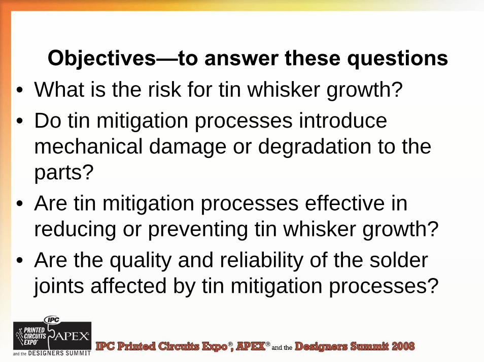
Post solder dip, pre-test evaluation
Cross section of SOT23 component after solder dip—excessive solder

Post solder dip, pre-test evaluation
Cross section of TSSOP lead after solder dip—no residual tin

Post solder dip, pre-test evaluation
Cross section of SOT23 lead after solder dip—no perceptible residual tin
Tin-lead solder SOT23 lead--
Kovar

Post solder dip, pre-test evaluation
Cross section of PLCC/J leads shows no damage or delamination but some cases of excessive solder

Post solder dip, pre-test evaluation
SEM examination of TSSOP showed no damage at lead egress. EDX was consistent with Sn63.

Post solder dip, pre-test evaluation
Cross section of ceramic chip part shows no cracks or damage to ceramic. Minimal solder coverage at corners—possible solderability issue
Metallization adhesion layer
NickelSolder
Ceramic body
Minimal solder coverage at corner

Post solder dip, Pre-test evaluation
Pure tin surfaces on connector leads were not fully mitigated due to lead/body configuration.Another concern: solder may wick up onto contact surfaces
Area where connector leads are housed in plastic—very difficult to replace tin coating with SnPb after connector has been built

Post solder dip, Pre-test evaluation
Tin surfaces on wrap-around leads of “low profile” capacitors were not fully mitigated due to tight of space between lead & body “Pb addition” process yielded Pb across all surfaces of leads
Tantalum capacitor with “wrap-around lead configuration
EDX analysis of pulled back leads revealed that solder dipped part had incomplete solder coverage

Post solder dip, pre-test evaluation
Lighter areas = Sn
Darker areas = Pb
SEM image of chip part after Pb addition—segregated tin/lead

Evaluation of tin whisker growth after CCA installation
and environmental test

Pre-test evaluation• All baselined PLCC, TSSOP, SOT23, chip parts were pure tin.• Tin whiskers observed on PLCC and TSSOP baseline parts. • Largest whisker on baseline parts was about 40 µm long. • Damaged, poor plating/coating quality was observed on
connectors, 0402, 1206, PLCC & SOT23 components.• On PLCC, TSSOP, SOT23 and chip parts mitigated by solder
dipping, pure tin material was completely removed and replaced with SnPb.
• No mechanical damage such as internal cracks, discoloration or delamination, was observed on the tin-mitigated parts.
• Solder dipping does not completely remove pure tin from “low profile” leaded components or connectors.
• Some parts showed excessive solder on the leads after the solderdipping process.
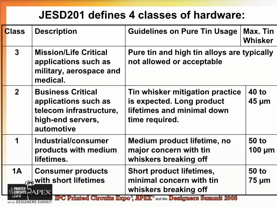
JESD201 defines 4 classes of hardware: Class Description Guidelines on Pure Tin Usage Max. Tin
Whisker3 Mission/Life Critical
applications such as military, aerospace and medical.
Pure tin and high tin alloys are typically not allowed or acceptable
Tin whisker mitigation practice is expected. Long product lifetimes and minimal down time required.
Medium product lifetime, no major concern with tin whiskers breaking offShort product lifetimes, minimal concern with tin whiskers breaking off
2 Business Critical applications such as telecom infrastructure, high-end servers, automotive
40 to 45 µm
1 Industrial/consumer products with medium lifetimes.
50 to 100 µm
1A Consumer products with short lifetimes
50 to 75 µm

Test & Inspection ConditionsCategory Description Details Reference
Test Conditions & Duration:1.Temperature cycling2.Ambient temperature/ humidity storage3.High temperature/humidity storage
-40°C to 85°C, 1000 cycles 30°C, 60% RH, 3000 hours
60°C, 87% RH, 3000 hours
JESD 22A121
Sample Size •Multi-leaded components: minimum of 96 terminations/6 components•Leadless components: minimum of 18 terminations/9 components
JESD201
Inspection magnification Minimum 50X for optical inspection, 250X for SEM.
JESD 22A121
Whisker density classification JESD 22A121
Whisker Density # Whiskers per leadLow < 10
Medium 10-45High > 45

Results—tin whisker growth
Tin whiskers on connector lead prior to solder dip

Results—tin whisker growth
25 µm whisker on pure tin PLCC piece part during 60°C, 87% RH test.

Results—tin whisker growth
Whiskers and nodules on tin plated control part--1206 capacitor--after 1000 temp cycles.

Results—tin whisker growth
Pure tin control part: 0402 resistor after 3000 hours 60°C, 87% RH. High densities of nodules and whiskers were observed, up to 100 µm

Results—tin whisker growth
36 µm whisker piercing conformal coat on 0402 resistor after 3000 hours 60°C, 87% RH
Presence or absence of urethane conformal coating did not significantly affect whisker length or density

Results—tin whisker growth
“Hillocks” on tin mitigated 1206 part after 1000 temp cycles

Results—tin whisker growth
Whiskers and nodules on pure tin PLCC after 3000 hours 30C, 60% RH

Results—tin whisker growth
39 µm tin whisker growing from PLCC piece part after 3000 hours 30C, 60% RH
Results—tin whisker growth
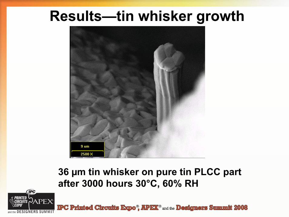
36 µm tin whisker on pure tin PLCC part after 3000 hours 30°C, 60% RH

Results—whisker growth
4 µm Pb whisker on tin mitigated 0402 chip after 1000 temp cycles

Results—whisker growth
1
2 3
≈10 µm whisker growing from tin mitigated TSSOP part after 1000 temp cycles Area 1 = PbArea 2 = SnArea 3 = SnPb

Results—Xray evaluation• Encapsulated modules and reballed BGAs could not be
visually or SEM inspected• X-ray analysis was attempted to discern whisker growth,
with resolution down to approximately 10 µm. • No whiskers were detected; BGA solder balls looked OK• Encapsulated modules passed electrical test.• Ceramic-filled coating and encapsulation may inhibit
proliferation of whiskers

Whisker Density
Part type ↓ Finish Baseline Post-Temp cycle test
Post-30°C, 60% RH test
Post-60°C, 87% RH test
Pure tin Medium High High/Med High/Med
SnPb None Low/Med Medium Medium
Pure tin High NA High High
SnPb None Low/Med Low Low
Pure tin Low Medium Medium Low
SnPb None Low Low Low
Pure tin NA High Low Medium
SnPb NA Low Medium Low
Pure tin NA NA Low Low
SnPb NA Low Low None
Pure tin Low High High High
SnPb None Low Medium Low
Pure tin High High High High
SnPb None Medium Medium Low
Pure tin Medium High Medium Low
SnPb Medium Medium High Low
connector
1206 chip
0402 chip
QFN64
DFN8
SOT23
PLCC
TSSOP
Summary of Whisker Density Data
Tin mitigation greatly reduces but does not eliminate whiskers.

Fig. 3 Tin Whisker Growth--pure tin vs. mitigated parts
0
20
40
60
80
100
TSSOP--tin
TSSOP--tin
lead
PLCC--t
in
PLCC--t
in lea
dQFN
64--ti
n
QFN64
--tin le
adSOT23
--tin
SOT23--ti
n lead
DFN8--tin
DFN8--tin
lead
0402
--tin
0402
--tin le
ad12
06--ti
n12
06--ti
n lead
FTSH conne
ctors-
-tin
FTSH conne
ctors-
-tin le
adM
ax. w
hisk
er le
ngth
(µm
)
BaselineAfter temp cycleAfter 30-60After 60-87
Pass/fail per JESD201 Class 2
Tin mitigation reduces length of whiskers by 3X to 15X

Fig. 4 Decrease in Whisker Size Due to Tin Mitigation & Span of Largest Whisker
0
20
40
60
80
100
TSSOP PLCC SOT23 DFN8 0402 1206 FTSH
Perc
ent
% Decrease in maximum whisker length due to tin mitigation% Lead Separation spanned by largest whisker on pure tin part% Lead Separation spanned by largest whisker on SnPb part
Largest whiskers spanned only 30% of span between conductors.

Test results: tin whisker growth• Temp cycling and temperature/humidity storage induced whisker growth. • Whiskers grew on all pure tin parts and most tin mitigated parts• No whiskers were observed to “short” between leads; the largest
percentage of lead separation spanned by a tin whisker was about 30%. • Whiskers pierced and grew along surfaces beneath urethane conformal
coating. • Among 7 part types tested in significant numbers, the decrease in
maximum whisker length effected by tin mitigation was 30 to 70% relative to the pure tin components.
• No significant differences in whisker density or size were noted among parts mitigated by tin mitigation suppliers/processes.
• No significant differences in whisker density or size were noted on parts installed on PWBs with different materials, pad finish or with air or nitrogen reflow atmosphere.
Tin mitigation severely limits whisker growth but does not completely eliminate tin whisker formation

Evaluation of solder joint reliability after
temperature cycling

Results--Solder joint evaluation
Cracked solder joint on 1206 chip resistor after 1000 temp cycles

Results--Solder joint evaluation
Cracked solder joint on 1206 chip resistor after 1000 temp cycles

Results--Solder joint evaluation
Cracked solder joint on PLCC solder joint after 1000 temp cycles

Results—solder joint reliability after 1000 cycles -40 to 85° C
• All part types except the DFN8 showed some cracks in the solder joints • Small qty of cracked solder joints appeared severe enough to impact CCA
reliability. No parts showed cracks on 100% of the leads.• No cracks or other anomalies were observed on the component bodies.• Damage was more widespread on larger components than smaller ones.• Solder joints on PLCCs installed on epoxy PWBs with silver finish reflowed
in air showed more cracks than on the other types of boards. • Among all part types, there were no consistent trends between solder joint
quality and PWB material, PWB pad finish or reflow condition.• No anomalies were noted on parts with non pure tin lead-free finishes
(SnBi, NiPDAu and AgPd). In very small sample sizes, parts with these finishes showed similar solder joint quality as tin mitigated components.
Robust solder joints can be made with components that have been through tin mitigation processes.

Discussion—Component Reliability• Most likely degradation mechanisms:
– Degraded solderability– Damaged interfaces, materials, and interconnects.– Degraded electrical performance, i.e. die-level
• Solder dip usually helps with solderability since there is a fresh coat of SnPb
• No component damage noted in SEM, Xray or cross section – Navy ManTech study also showed no degradation
• Automated solder dip process recommended– Much better controls than manual dipping
Well-controlled tin mitigation processes will not adversely affect the types of parts studied in this report.

Findings & Conclusions• Automated solder dip/Pb addition effectively replaced Sn with SnPb on
exposed Sn leads • Tin mitigation processes did not induce damage on parts. • Cracked solder joints were observed on about ½ of the parts.• No catastrophic solder joint failures on tin mitigated parts or lead-free
parts after 1000 temperature cycles. • Whiskers grew on almost all of the parts, even SnPb surfaces. • Maximum whisker length on tin mitigated parts was 30 to 70% smaller
than on pure tin parts. • Pb and “mixed” SnPb whiskers were also observed. • Whiskers grew beneath and through conformal coatings. • Tin mitigation supplier, PWB material, pad pattern or solder reflow
condition had little effect on tin whisker growth or solder joint cracking.
Tin whisker tests failed on all but 2 pure tin component types and passed on all tin-mitigated component types

Recommendations• Approve pure tin and SnBi parts for limited use as long as
their leads/ terminations are mitigated prior to installation. • Approve NiPdAu parts—no mitigation needed. • Parts selection team should request/require JESD201 test
data from component suppliers for all pure tin parts. • Low profile components, encapsulated parts and many
connectors cannot be completely mitigated – Need to be evaluated on a case-by-case basis.
• Mechanical parts, radial leaded parts, parts with glass seals or special sensitivities to heat or ESD (<100 V) were not covered by this study– Need to be evaluated separately.

Recommendations on dealing with Lead-Free PartsOption Advantages DisadvantagesFind alternate equivalent part
May be “drop-in”
Guaranteed quantities
Can change parts
Mitigation Avoid redesign & last time buys
Extra handling, processing & costMay not eliminate all risks
Avoid redesign & last time buys
May require approval
“Last time buy” on part before it becomes lead-free
Up-front costAccurate forecast may not be possible
Redesign Cost, schedule
Qualify new parts/finishes
May not be offered by suppliersExtensive cost & technical obstacles