Embed Size (px)
Citation preview
Slide 1
1
EI1009 – LINEAR INTEGRATED CIRCUITS AND APPLICATIONS
Dr.K.A.Sunitha
A.P(Sr.G)
EIE Department
SRM University
Slide 2 What is this subject all about?
• Title ?
• Why?
• When and where ?
Slide 3
• What is an Integrated Circuit?
• Where do you use an Integrated Circuit?
• Why do you prefer an Integrated Circuit to the circuits made
by interconnecting discrete components?
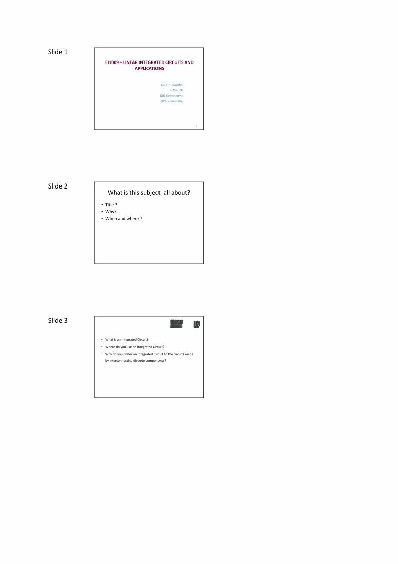
Slide 4 The Integrated Circuit (IC)
• An IC consists of interconnected electronic components in a single piece (“chip”) of semiconductor material.
The first planar IC(actual size: 0.06 in. diameter)
• In 1959, Robert Noyce (Fairchild Semiconductor) demonstrated an IC made in silicon using SiO2
as the insulator and Al for the metallic interconnects.
• In 1958, Jack S. Kilby (Texas Instruments) showed that it was possible to fabricate a simple IC in germanium.
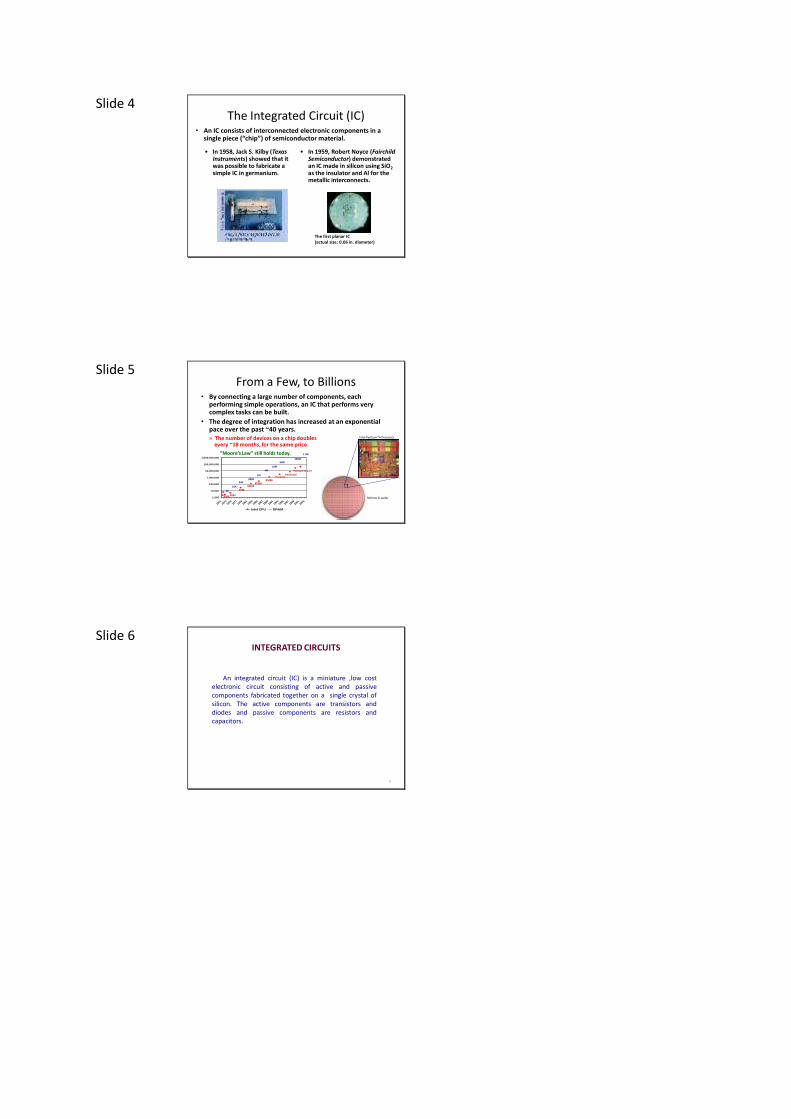
Slide 5 From a Few, to Billions
• By connecting a large number of components, each performing simple operations, an IC that performs very complex tasks can be built.
• The degree of integration has increased at an exponential pace over the past ~40 years.» The number of devices on a chip doubles
every ~18 months, for the same price.
“Moore’s Law” still holds today.
1,000
10,000
100,000
1,000,000
10,000,000
100,000,000
1,000,000,000
1971
1973
1975
1977
1979
1981
1983
1985
1987
1989
1991
1993
1995
1997
1999
2001
2003
Intel CPU DRAM
4044 8080
8086
80486
PentiumPentiumII
8028680386
Pentium III & IV
1K 4K
16K
64K
256K
1M
4M
16M
64M
256M
1 Gb
300mm Si wafer
Intel Pentium®4 Processor
Slide 6
6
An integrated circuit (IC) is a miniature ,low costelectronic circuit consisting of active and passivecomponents fabricated together on a single crystal ofsilicon. The active components are transistors anddiodes and passive components are resistors andcapacitors.
INTEGRATED CIRCUITS

Slide 7 Why “LINEAR” INTEGRATED CIRDUITS…?
• A linear integrated circuit (linear IC) is a solid-state analog device characterized by a theoretically infinite number of possible operating states. It operates over a continuous range of input levels. In contrast, a digital IC has a finite number of discrete input and output states.
Slide 8
8
WHY….Advantages of integrated circuits
1. Miniaturization and hence increased equipment density.
2. Cost reduction due to batch processing.
3. Increased system reliability due to the elimination of soldered joints.
4. Improved functional performance.
5. Matched devices.
6. Increased operating speeds.
7. Reduction in power consumption
Slide 9
• Communication
• Control
• Instrumentation
• Computer
• Electronics
WHERE?
Applications of an Integrated Circuit
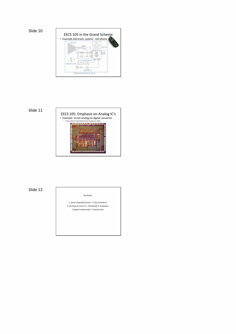
Slide 10 EECS 105 in the Grand Scheme
• Example electronic system: cell phone
Slide 11 EECS 105: Emphasis on Analog IC’s
• Example: 14-bit analog-to-digital converter– Y. Chiu, IEEE Int’l Solid-State Circuits Conference, 2004.
Slide 12 Text Books:
1. Linear Integrated Circuits – D. Roy Choudhury
2. Op-Amps & Linear ICs – Ramakanth A. Gayakwad.
3. Digital Fundamentals – Floyd and Jain

Slide 13 Classification
• Digital ICs
• Linear ICs
Pn junctionisolation
Hybrid circuits
Integrated circuits
Dielectricisolation
Monolithic circuits
Bipolar Uni polar
MOSFET JFET
Classification of ICs
Thick &Thin film
Slide 14 Chip size and Complexity
• Invention of Transistor (Ge) - 1947
• Development of Silicon - 1955-1959
• Silicon Planar Technology - 1959
• First ICs, SSI (3- 30gates/chip) - 1960
• MSI ( 30-300 gates/chip) - 1965-1970
• LSI ( 300-3000 gates/chip) -1970-1975
• VLSI (More than 3k gates/chip) - 1975
• ULSI (more than one million active devices are integrated on single chip)
Slide 15
SSI MSI LSI VLSI ULSI
< 100 active
devices
100-1000
active
devices
1000-
100000
active
devices
>100000
active
devices
Over 1
million
active
devices
Integrated
resistors,
diodes &
BJT’s
BJT’s and
Enhanced
MOSFETS
MOSFETS 8bit, 16bit
Microproces
sors
Pentium
Microproces
sors

Slide 16 IC Package types
• Metal can Package
• Dual-in-line
• Flat Pack
Slide 17 Metal can Packages
• The metal sealing plane is at the bottom over which the chip is bounded
• It is also called transistor pack
Slide 18 Doul-in-line Package
• The chip is mounted inside a plastic or ceramic case
• The 8 pin Dip is called MiniDIP and also available with 12, 14, 16, 20pins
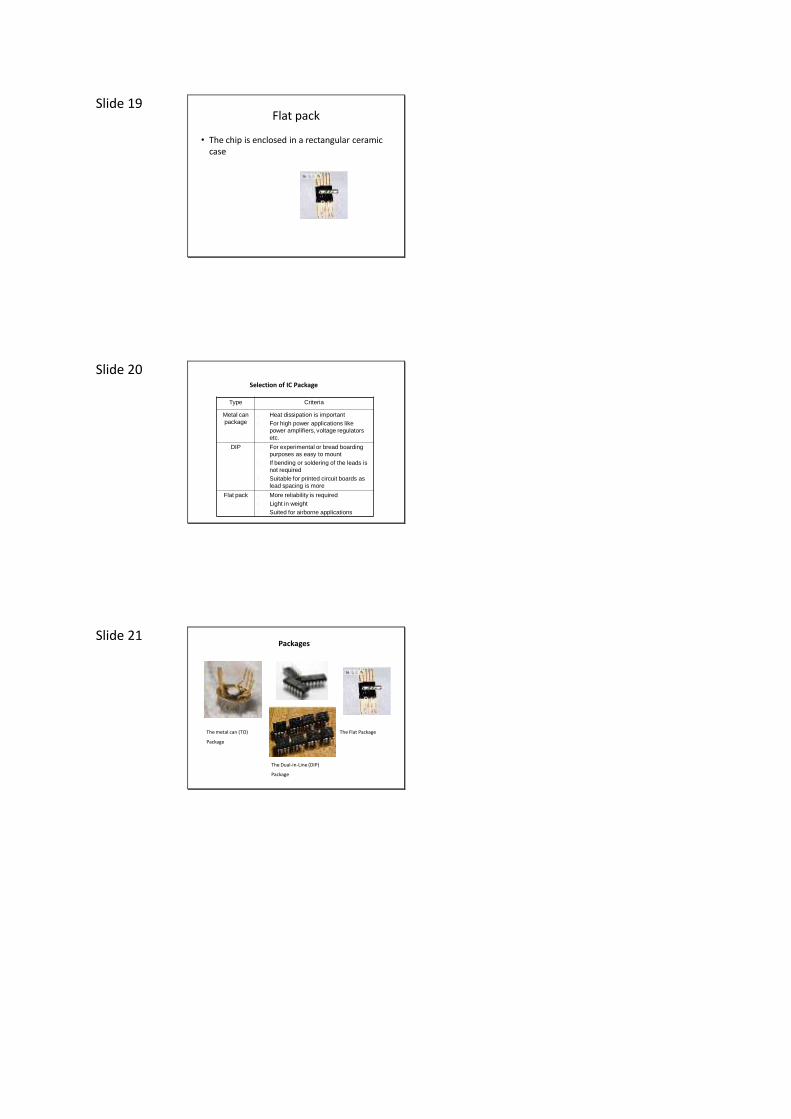
Slide 19 Flat pack
• The chip is enclosed in a rectangular ceramic case
Slide 20 Selection of IC Package
Type Criteria
Metal can
package
1. Heat dissipation is important
2. For high power applications like
power amplifiers, voltage regulators
etc.
DIP 1. For experimental or bread boarding
purposes as easy to mount
2. If bending or soldering of the leads is
not required
3. Suitable for printed circuit boards as
lead spacing is more
Flat pack 1. More reliability is required
2. Light in weight
3. Suited for airborne applications
Slide 21
The metal can (TO)
Package
The Dual-in-Line (DIP)
Package
The Flat Package
Packages
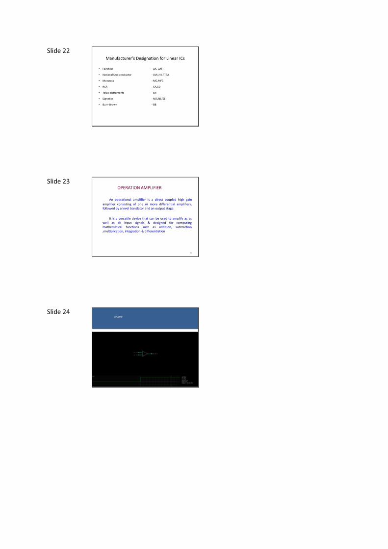
Slide 22 Manufacturer’s Designation for Linear ICs
• Fairchild - µA, µAF
• National Semiconductor - LM,LH,LF,TBA
• Motorola - MC,MFC
• RCA - CA,CD
• Texas Instruments - SN
• Signetics - N/S,NE/SE
• Burr- Brown - BB
Slide 23 OPERATION AMPLIFIER
An operational amplifier is a direct coupled high gain
amplifier consisting of one or more differential amplifiers,followed by a level translator and an output stage.
It is a versatile device that can be used to amplify ac aswell as dc input signals & designed for computingmathematical functions such as addition, subtraction,multiplication, integration & differentiation
23
Slide 24 OP AMP

Slide 25
OP AMP WITH FEED BACK
Slide 26 Op-amp symbol
26
Non-inverting input
inverting input
0utput
+5v
-5v
2
3
67
4
Slide 27 Ideal characteristics of OPAMP
1. Open loop gain infinite
2. Input impedance infinite
3. Output impedance zero
4. Bandwidth infinite
5. Zero offset, ie, Vo=0 when V1=V2=0
6. Infinite CMRR
7. Infinite Slew Rate
27

Slide 28 Inverting Op-Amp
V VR
ROUT IN
f
1
28
Slide 29
INVERTING AMPLIFIER
Slide 30 Non-Inverting Amplifier
Vout= (1+Rf/R1)Vin
30

Slide 31
NON - INVERTING AMPLIFIER
Slide 32 Voltage follower
32
Slide 33
VOLTAGE FOLLOWER
Slide 34 DC characteristics
Input offset currentThe difference between the bias currents at the
input terminals of the op- amp is called as input offsetcurrent. The input terminals conduct a small value ofdc current to bias the input transistors. Since the inputtransistors cannot be made identical, there exists adifference in bias currents
34
Slide 35 DC characteristics
Input offset voltage
A small voltage applied to the input terminals to makethe output voltage as zero when the two input terminals aregrounded is called input offset voltage
35
Slide 36 DC characteristics
Input offset voltage
A small voltage applied to the input terminals to make theoutput voltage as zero when the two input terminals aregrounded is called input offset voltage
36

Slide 37 DC characteristics
Input bias current
Input bias current IB as the average value of the base currents entering into terminal of an op-amp
IB=IB+ + IB
-
2
37
Slide 38 DC characteristics
THERMAL DRIFT
Bias current, offset current and offset voltage changewith temperature. A circuit carefully nulled at 25oc may notremain so when the temperature rises to 35oc. This is calleddrift.
38
Slide 39 AC characteristics
39
Frequency Response
HIGH FREQUENCY MODEL OF OPAMP
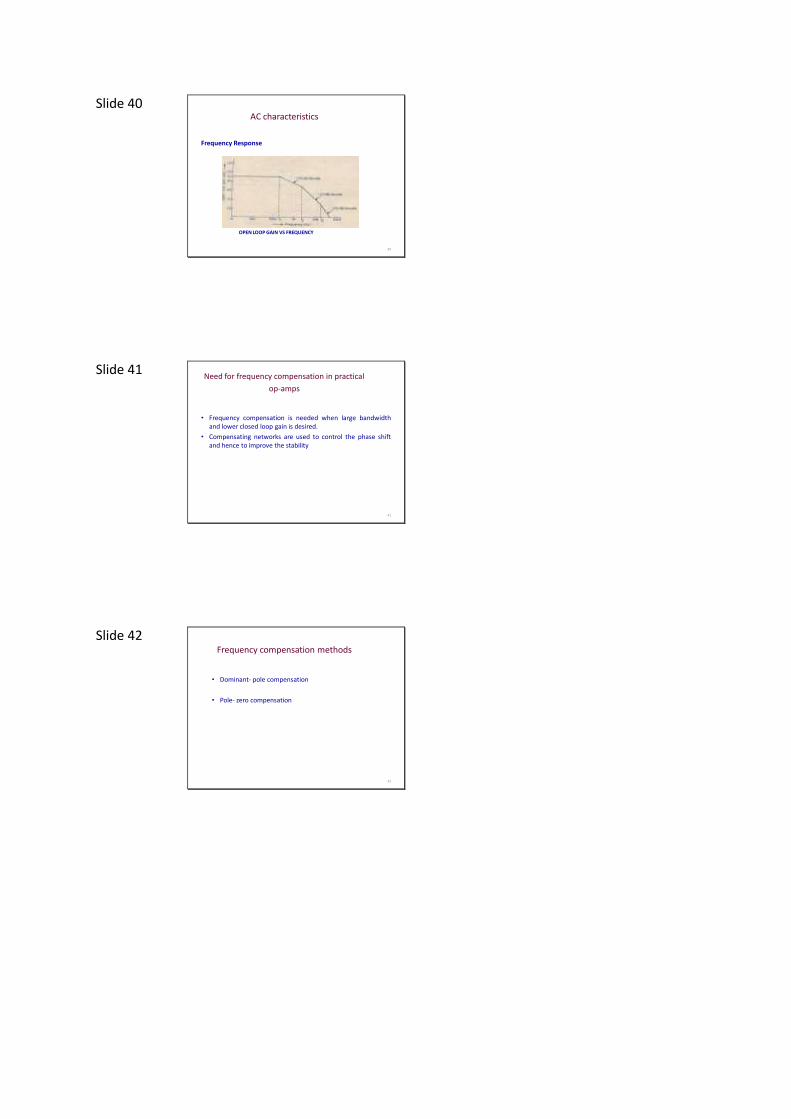
Slide 40 AC characteristics
40
Frequency Response
OPEN LOOP GAIN VS FREQUENCY
Slide 41 Need for frequency compensation in practical
op-amps
• Frequency compensation is needed when large bandwidthand lower closed loop gain is desired.
• Compensating networks are used to control the phase shiftand hence to improve the stability
41
Slide 42 Frequency compensation methods
• Dominant- pole compensation
• Pole- zero compensation
42

Slide 43 Slew Rate
• The slew rate is defined as the maximum rate of change of
output voltage caused by a step input voltage.
• An ideal slew rate is infinite which means that op-amp’soutput voltage should change instantaneously in response toinput step voltage
43
Slide 44 Instrumentation Amplifier
In a number of industrial and consumer applications, themeasurement of physical quantities is usually done with thehelp of transducers. The output of transducer has to beamplified So that it can drive the indicator or display system.This function is performed by an instrumentation amplifier
44
Slide 45 Instrumentation Amplifier
45
Slide 46 Features of instrumentation amplifier
1. high gain accuracy
2. high CMRR
3. high gain stability with low temperature co-efficient
4. low dc offset
5. low output impedance
46
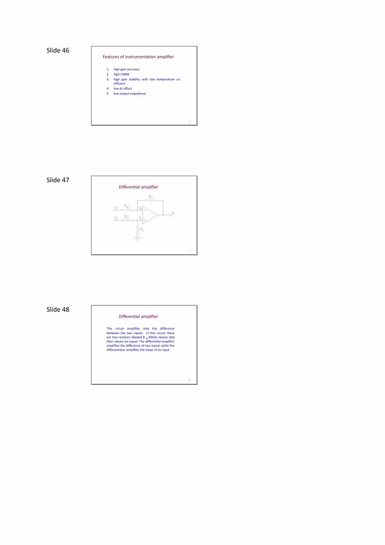
Slide 47 Differential amplifier
47
Slide 48 Differential amplifier
This circuit amplifies only the difference
between the two inputs. In this circuit thereare two resistors labeled R IN Which means thattheir values are equal. The differential amplifieramplifies the difference of two inputs while thedifferentiator amplifies the slope of an input
48

Slide 49
DIFFERENTIAL AMPLIFIER
Slide 50 Summer
50
Slide 51
SUMMING AMPLIFIER