Embed Size (px)
Citation preview
Eindhoven University of Technology
MASTER
One cycle control used in a class-D power amplifier
el Farissi, H
Award date:2007
Link to publication
DisclaimerThis document contains a student thesis (bachelor's or master's), as authored by a student at Eindhoven University of Technology. Studenttheses are made available in the TU/e repository upon obtaining the required degree. The grade received is not published on the documentas presented in the repository. The required complexity or quality of research of student theses may vary by program, and the requiredminimum study period may vary in duration.
General rightsCopyright and moral rights for the publications made accessible in the public portal are retained by the authors and/or other copyright ownersand it is a condition of accessing publications that users recognise and abide by the legal requirements associated with these rights.
• Users may download and print one copy of any publication from the public portal for the purpose of private study or research. • You may not further distribute the material or use it for any profit-making activity or commercial gain
__-We technische universiteit eindhoven
Capaciteitsgroep Elektrische EnergietechniekElectromechanics & Power Electronics
Master of Science Thesis
One Cycle Control used in aclass-D power amplifier
Hommad el FarissiEPE.2oo7·A.o3
The department Electrical Engineering
ofthe Technische Universiteit Eindhoven
does not accept any responsibility
for the contents ofthis report
Coaches:
Dr. Jorge Duarte (TVIe)Dr.ir. Frank van Horck (Philips Power Solutions, TV Ie)
December 2006
I faculteit elektrotechniek
Abstract
Nowadays power converters such as computer batteries, television power supplyunits, audio amplifiers etc., are designed according to a switched-mode principle. This de- notes that the power conversion is achieved by switching the inputvoltage on and off with a certain ratio such that the desired output voltage isreached. These converters are usually controlled with Pulse Width Modulation(PWM). PWM is the control method whereby the switch on/of times (i.e pulsewidth) are adapted continuously to regulate the output voltage. Traditionally,this control method uses a linear feed- back to control certain state variables inthe switched-mode converter.
This report presents a detailed analyse of the One-cycle control method. Theoretical analysis show that the controller is able to control the duty-ratio in realtime such that in each switching cycle the average of the chopped waveform atthe switch output is exactly equal to the control reference. These analysis include simulations of the OCC used to control a buck converter and a full-bridgeamplifier. A detailed analyses for component sensitivity is also presented for thecontroller.
Beside the theoretical analyses, practical measurements are performed to verifythe theoretical results. The OCC is designed and implemented on a PCB andused to control a class-D power stage. The performance of the OCC power amplifier is then compared to the UCD power amplifier. As a result the experimentshave shown that OCC power amplifier performs slightly better than the UCDamplifier.
Finally the OCC power amplifier is extended with the addition of an outputfeedback. The output feedback is added to compensate for the disturbances inthe output load and to reduce the offset in the output voltage.

Acknowledgements
I would like to express my appreciation and gratitude to the following people fortheir help in conducting the graduation project.
First of all, I wish to thank Prof. Dr. Ir. Andre Vandenput and Ir. M.A.M.Hendrix for allowing me to perform my graduation project in the EPE group.
I would also like to thank my supervisors Dr. Jorge Duarte and Dr.Ir. Franckvan Horck for their calm and patience guidance during my graduation period toassist me to gain insight and experience in solving real engineering issues.
Furthermore, I would like to extend my appreciation to the Philips Power Solutions employees for creating a pleasant work environment that is hard to forget.And spe- cial thanks goes to Marijn Uytdewilligen for his support with the PCBdesign.
Last but not least, I would like to thank my parents and my close friends fortheir support and inspirations during my studies.
Hommad EI FarissiEindhoven, the NetherlandsDecember 2006
ii

Contents
1 Introduction1.1 Objective and outline.
2 acc theory2.1 Principle of OCC . . . . . . . . . . .2.2 One-cycle control of a buck converter2.3 Drawbacks of the conventional OCC
3 Improved one-cycle control3.1 Theory .3.2 Pulse width modulation, double-edge3.3 Improved one-cycle control circuit
3.3.1 Resetable integrator3.3.2 Error integrator . . .3.3.3 Adder circuit .. . .
3.4 Sensitivity of the controller.3.4.1 Error integrator . . .3.4.2 Adder circuit ....3.4.3 Resetable Integrator
3.5 Delay time and its impact on the performance
4 Simulations
5 Practical Implementation5.1 Controller implementation5.2 Time domain signal measurement
6 Results6.1 THD+N measurement6.2 FFT analysis . . . . .6.3 THD+N Icepower . . .6.4 EMC and ground loops.
III
12
44
6
8
99
1216192224
25252627
27
29
3434
36
4040
43
4546

7 Closed loop control7.1 Output feedback7.2 Low-pass filter ..7.3 Phase lead compensation
8 Conclusions and recommendations
Appendices
A Pcad Schematic
B Closed loop feedback schematic
C Matlab code: calculation of the resetable integrator voltage
D Matlab code: calculation of is variation due to supply ripple
E Matlab code: calculation of the loop / error integrator voltage
IV
47474851
55
60
60
63
64
66
68
List of Figures
2.1 OCC constant frequency switch . . . . . . . . . . . . . . . . . . . .. 42.2 Waveforms of the One-cycle controlled constant frequency switch in
case of a constant reference signal.. . . . . . . . . . . . . . . . . . .. 52.3 One-cycle control of a buck converter . . . . . . . . . . . . . . . . .. 62.4 OCC buck converter, constant vrej, step in Vg of 10V, Lo = 50j1H, Co =
10j1F, Ro = 100, Ri = 1kO, Ci = 10nF, Vrej = 7V, Vg = 10V ..... 72.5 OCC buck converter, constant ~, variable Vrej, Lo = 50j1H, Co =
10j1F, Ro = 100, Ri = 1kO, Ci = lOnF, Vrej = 4 + 2sin(wt), ~ = 7V 8
3.1 Improved one-cycle control concept . . . . . 93.2 Waveforms of the improved control method. 103.3 Complete OCC conceptual diagram . . . . . 113.4 pulse width modulation types with fixed frequency 123.5 Pulse centre is modulated 133.6 Pulse centre is fixed. . . . . . . . . . 133.7 Double-edge modulation . . . . . . . 143.8 is variation caused by supply ripple . 153.9 is variation caused by changing ~ej 153.10 OCC used in a full-bridge amplifier . 163.11 Double-edge modulated implementation of the OCC . 173.12 Double-edge modulation theoretical waveforms. . . . 183.13 Resetable integrator circuit. . . . . . . . . . . . . . . 193.14 Resetable integrator output voltage (R1 = R2 = 1kw, R3 = R4 =
200wVg = 70 + 5 * sin(w * t)) 203.15 Simplified current model . . 213.16 Limitation of the duty-ratio . 223.17 Differential error integrator. . 233.18 Differential integrator operating stages. 233.19 Adder circuit .. . . . . . . . . . . . . 253.20 Error integrator fault . . . . . . . . . . 263.21 Influence of a delay in the error integrator 28
4.1 OCC used in a full-bridge amplifier 294.2 Open loop full-bridge amplifier. . 30
VI
4.3 aee compared to open loop control for different reference voltages 314.4 PSRR for different switching frequencies . . . . . . . . . 314.5 PSRR and switching frequency versus delay-time .... 324.6 PSRR for different ripple frequencies in the input voltage 32
5.1 Implementation of the OCC power amplifier with output feedback loop 345.2 Measurement setup with the Audio Precision instrument . . 365.3 Input and amplified output voltage (50x attenuation), 30 W 375.4 Square wave power stage voltage outputs. . . . . . 375.5 Differential error integrator voltage . . . . . . . . . . . . . . 385.6 Resetable integrator voltage and switch drive signal . . . . . 395.7 Resetable integrator voltage and comparator output voltage 39
6.1 THD+N versus power, OCC and UCD power amplifier, 4 Ohm load. 406.2 THD+N versus power, OCC and UCD power amplifier, 8 Ohm load. 416.3 THD+N versus amplitude, OCC and UCD power amplifier, no load 416.4 Gain versus frequency plot . . . . . . . . . . . . . . . . . . . 426.5 FFT of the OCC power amplifier, 10 mW, THD+N = 0.14% 436.6 FFT of the UCD power amplifier, 10 mW, THD+N = 0.19% 446.7 FFT of the OCC power amplifier, 10 W, THD+N = 0.14% 446.8 FFT of the UCD power amplifier, 10 W, THD+N = 0.21% 456.9 THD+N versus power, Icepower, 8 Ohm load .... 456.10 THD+N versus amplitude, influence of EMI on THD 46
7.1 Closed-loop OCC amplifier circuit. . . . . 477.2 Circuit scematic of the UCD power-stage. 487.3 Simplified schematic of the low-pass filter. 497.4 Open-loop bode plot for the OCC power amplifier, 8 n load 497.5 Open-loop OCC + power-stage measured with a spectrum analyzer 507.6 Open-loop low-pass filter measured with a spectrum analyzer. 517.7 One-cycle control FFT plots. . . . 517.8 ucd THD verus power, 4 n load . . . . . . . . . . . . . . . . . 527.9 Closed-loop OCC + power-stage. . . . . . . . . . . . . . . . . 537.10 THD+N verus power for differnt closed-loop feedback gains, 8 n load 547.11 THD+N verus power OCC with and without output feedback and
UCD, 8n load. . . . . . . . 54
A.1 Pcad schematic of the OCCA.2 Pcad PCB layout of the OCC
B.1 Feedback schematic . . . . . .
Vll
6062
63

List of Tables
3.1 PSRR (dB) for different component tolerances in the error circuit 263.2 PSRR (dB) for different component tolerances in the adder circuit 273.3 PSRR (dB) for different component tolerances 27
5.1 System parameters of the circuit. . . . . . . . 35
7.1 Offset in output voltage for different feedback gains 53
A.1 List of components in the oee circuit 61
B.1 List of components feedback circuit .. 63
Vlll
Chapter 1
Introduction
Nowadays power converters such as computer batteries, television power supply units,audio amplifiers etc., are designed according to a switched-mode principle. This denotes that the power conversion is achieved by switching the input voltage on and offwith a certain ratio such that the desired output voltage is reached. These convertersare usually controlled with Pulse Width Modulation (PWM). PWM is the controlmethod whereby the switch on/off times (i.e pulse width) are adapted continuouslyto regulate the output voltage. Traditionally, this control method uses a linear feedback to control certain state variables in the switched-mode converter.
In this conventional feedback control, the duty-ratio is linearly modulated in adirection that reduces the error. When the power source voltage is perturbed, forexample by a large step up, the duty-ratio control does not see the change instantaneously since the error signal must change first. Therefore a typical transientovershoot will be observed at the output voltage. The duration of the transient isdictated by the loop gain bandwidth. As a consequence, a large number of switchingcycles is required before the steady-state is regained.
On the other hand, nonlinear control of PWM switch-mode converters, in comparison to linear feedback, has shown excellent improvements such as optimizingsystem response, reducing the distortion and rejecting power supply disturbances.One of these nonlinear control methods is One Cycle Control (OCC).
The original oee concept was proposed by Dr. Smedley in 1991[2]. The technique is conceived to control the duty-ratio in real time such that in each cycle theaverage of the chopped waveform at the switch output is exactly equal to the controlreference. As a result the the oee should be able to fully reject the perturbationsin the power supply and follow the reference signal exactly [2].Its fast response, low distortion and good power supply ripple rejection makes thiscontrol method interesting for many converters, especially for those that need accurate power supplies.
1

2 Chapter 1. Introduction
1.1 Objective and outline
The goal of this Master's thesis is to provide a theoretical analysis and a practicalverification of the One Cycle Control method used in an audio power amplifier.
Purposely, an audio amplifier is chosen since this application is more sophisticatedthan other switched-mode applications. Furthermore, it needs to satisfy certain criteria such as a low THD and good PSRR (Power Supply Ripple Rejection). Thesecriteria can be used to assess the performance of the ane Cycle Controller.
This report presents the results of my graduation assignment, which consists ofthe following parts:
1. A literature research on the acc method used in an audio class-D amplifier.
2. Evaluation of the control method of the acc.
3. The design and implementation of the acc in a class-D amplifier.
This report is structured as follows:
Chapter 2:Description of the working and simulation of acc principle.
Chapter 3:Description of the improved acc principle.
Chapter 4:Simulation of the improved acc.
Chapter 5:Description of the implementation of the acc in a class-D amplifier.
Chapter 6:Presentation of the experimental results.
Chapter 7:Description of the additional outer feedback loop
Chapter 8:Conclusions of the graduation assignment and recommendations for future work.
Chapter 2
acc theory
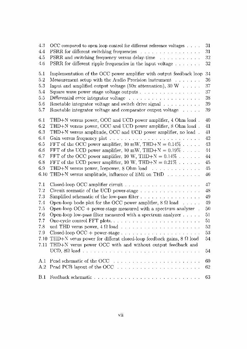
2.1 Principle of accA circuit showing the principle of aee is depicted in Fig. 2.1. A constant frequencyclock is used to turn on the switch at the beginning of the cycle. The switched variabley(t) is integrated and compared with a control reference. When the integrated valueof the switched variable reaches the control reference, the comparator turns off theswitch and resets the integrator to zero. This way, the integrated value of y(t)equals the control reference within every cycle. As a result, the average value of y(t),< y(t) >, is equal or proportional to the control reference, since the period of theswitched variable is imposed to be constant.
x(t) y(t)0>----------- .r--------------,
reset
Vrfj
comparator
Vim
integrator
Figure 2.1: aee constant frequency switch
The waveforms illustrated in Fig. 2.2 provide a good insight in the operatingprinciple. As shown in the figure the input voltage x(t) is a function of time and vref
is chosen constant. As a result, the time (ton) for the resetable integrator signal Vint
4
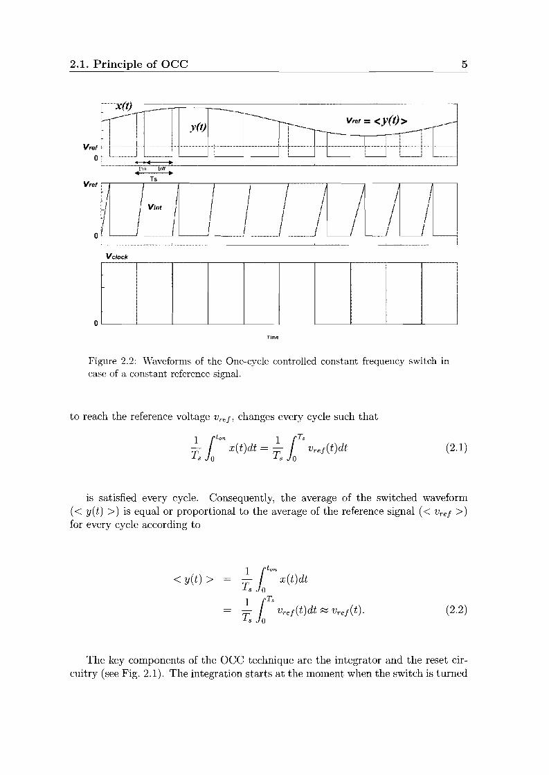
2.1. Principle of acc 5
Vref =<y(t)>
----'--------~-------_.---------'
y(t)
r--x(tr----=-..=::;:::::;==::;::::::;::=---------·-··-~ciL
0,
it ... •
ton toftof ~
Vref ,.......,-__---r-'Tc.::.s_--.__---. ,--__.....-__-,-__----.__----.,--_----,-__
Vref Lo!L--~!:::::;:;;:i_------l----~---~-------l
Vclock
o~_._ _'_______"_______.L.._____'_____--'--__---'-__---'-__---'-__--->__~
Tim!!!
Figure 2.2: \Vaveforms of the One-cycle controlled constant frequency switch incase of a constant reference signal.
to reach the reference voltage vre!' changes every cycle such that
1 lton 1 iTsT x(t)dt = T Vre!(t)dt
s 0 s 0(2.1)
is satisfied every cycle. Consequently, the average of the switched waveform« y(t) » is equal or proportional to the average of the reference signal « Vre! »for every cycle according to
< y(t) >1 ton
TsJ
ox(t)dt
1 iTsT vre!(t)dt ~ Vre!(t).
s 0(2.2)
The key components of the acc technique are the integrator and the reset circuitry (see Fig. 2.1). The integration starts at the moment when the switch is turned
6 Chapter 2. GCC theory
on by the fixed frequency clock pulse. The integrated value,
r Ts
Vint(t) = k Jo x(t)dt (2.3)
is compared with the control reference Vrej(t) instantaneously, where k is a constant and d = ton/Ts the duty-ratio. At the instant when the integrated value Vint(t)reaches the control reference Vrej(t), the switch changes from the on state to the offstate. At the same time, the controller resets the integrator to zero. The corresponding duty-ratio can be determined by examining
fdTs
k Jo x(t)dt = Vrej(t). (2.4)
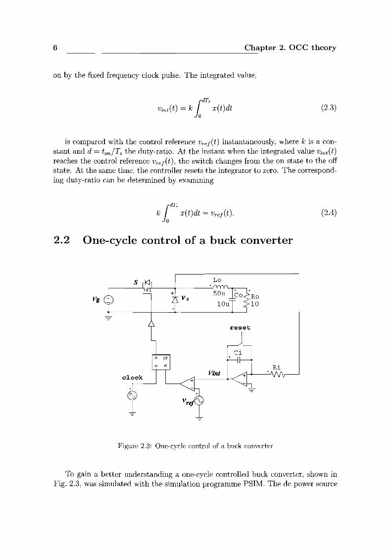
2.2 One-cycle control of a buck converter
Ci
Lo
Ro10
reset
RiVint
Vg
Figure 2.3: One-cycle control of a buck converter
To gain a better understanding a one-cycle controlled buck converter, shown inFig. 2.3, was simulated with the simulation programme PSIM. The dc power source
2.2. One-cycle control of a buck converter 7
voltage is ~ and the switch S are operated with a constant frequency. The converterworks as follows. When the switch S is on, the diode is off, and the diode-voltageV s equals the power source voltage ~ . When the switch S is off, the diode is on,and the diode-voltage, is zero. The power source voltage is chopped by the switchresulting in a switching variable V s ' The low-pass filter then attenuates the switchingfrequency and a dc output voltage, proportional to the reference input, is the result.
The MOSFET is turned on at the beginning of each switching period by a constant frequency clock. The diode-voltage is integrated and compared with a controlreference, the comparator changes its state. As a result, the MOSFET is turned offand the integrator is reset to zero. The power source voltage ~, diode-voltage V s ,
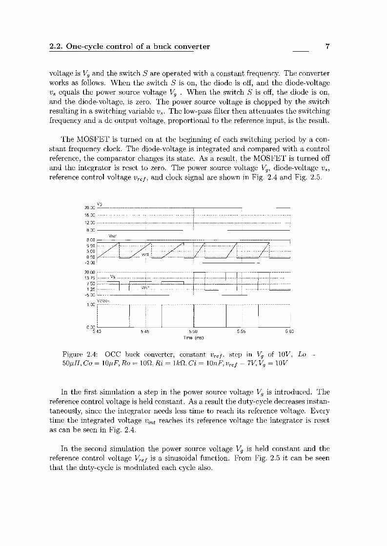
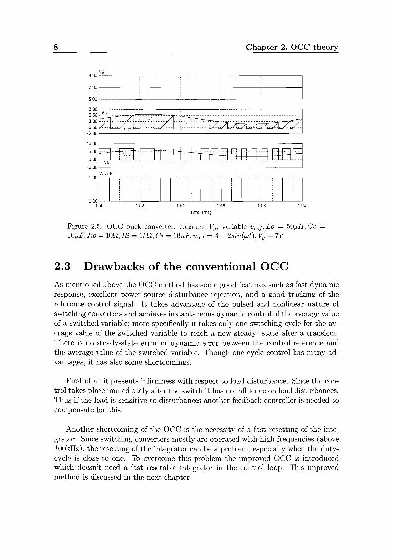
reference control voltage Vrej, and clock signal are shown in Fig. 2.4 and Fig. 2.5.
~::: r----:--immmim mmmm mm:8.00b, I
Vref
~mt=tLltltf]-=±f~\idock::0 ml . I- em II
5~ 5~ 5.~ 5~ 5~
TIme (ms)
Figure 2.4: aee buck converter, constant Vrej, step in Vg of lOV, Lo50f-LH, Co = lOf-LF, Ro = 100, Ri = lkO, Ci = lOnF, Vrej = 7V, Vg = lOV
In the first simulation a step in the power source voltage Vg is introduced. Thereference control voltage is held constant. As a result the duty-cycle decreases instantaneously, since the integrator needs less time to reach its reference voltage. Everytime the integrated voltage Vint reaches its reference voltage the integrator is resetas can be seen in Fig. 2.4.
In the second simulation the power source voltage Vg is held constant and thereference control voltage 1!;.ej is a sinusoidal function. From Fig. 2.5 it can be seenthat the duty-cycle is modulated each cycle also.
8 Chapter 2. acc theory
Vq900,::··· ---_ _--_..
i7.00 f-!-----'------'------;------'-----
500 I _. __~ _
1.601 581.56154152000 ~_'__~__L---.J~.L___'____'_----.l._ _'____'_____"_---'-~'_...L__L_--'-____'_ _'______'__.J
1.50
Time (ms)
Figure 2.5: aee buck converter, constant Vg , variable Vrej, Lo = 50j.LH, Co =
lOj.LF, Ro = 100, Ri = lkO, Ci = lOnF, Vrej = 4 + 2sin(wt), Vg = 7V
2.3 Drawbacks of the conventional accAs mentioned above the aee method has some good features such as fast dynamicresponse, excellent power source disturbance rejection, and a good tracking of thereference control signal. It takes advantage of the pulsed and nonlinear nature ofswitching converters and achieves instantaneous dynamic control of the average valueof a switched variable; more specifically it takes only one switching cycle for the average value of the switched variable to reach a new steady- state after a transient.There is no steady-state error or dynamic error between the control reference andthe average value of the switched variable. Though one-cycle control has many advantages, it has also some shortcomings.
First of all it presents infirmness with respect to load disturbance. Since the control takes place immediately after the switch it has no influence on load disturbances.Thus if the load is sensitive to disturbances another feedback controller is needed tocompensate for this.
Another shortcoming of the aee is the necessity of a fast resetting of the integrator. Since switching converters mostly are operated with high frequencies (above100kHz), the resetting of the integrator can be a problem, especially when the dutycycle is close to one. To overcome this problem the improved aee is introducedwhich doesn't need a fast resetable integrator in the control loop. This improvedmethod is discussed in the next chapter
Chapter 3
Improved one-cycle control
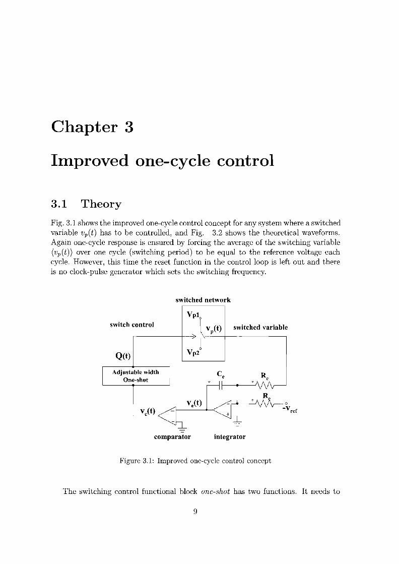
3.1 Theory
Fig. 3.1 shows the improved one-cycle control concept for any system where a switchedvariable vp(t) has to be controlled, and Fig. 3.2 shows the theoretical waveforms.Again one-cycle response is ensured by forcing the average of the switching variable(vp (t)) over one cycle (switching period) to be equal to the reference voltage eachcycle. However, this time the reset function in the control loop is left out and thereis no clock-pulse generator which sets the switching frequency.
switched network
switch control
Q(t)
Vpl
Lv/t) switched variahle
r----+------<>-1Vp2
Adjustable widthOne-shot
v (t)
Ce Re
comparator integrator
Figure 3.1: Improved one-cycle control concept
The switching control functional block one-shot has two functions. It needs to
9
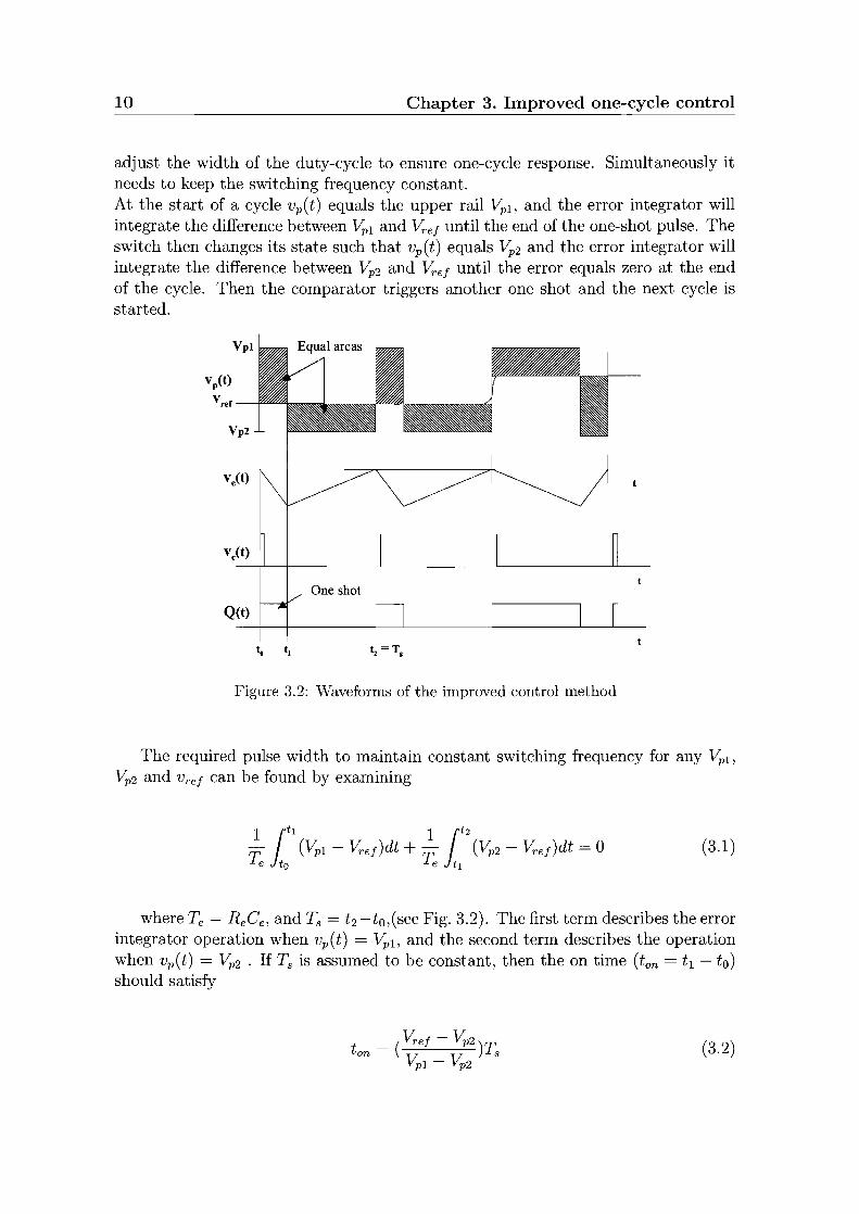
10 Chapter 3. Improved one-cycle control
adjust the width of the duty-cycle to ensure one-cycle response. Simultaneously itneeds to keep the switching frequency constant.At the start of a cycle vp(t) equals the upper rail Vp1 , and the error integrator willintegrate the difference between ~l and ~ef until the end of the one-shot pulse. Theswitch then changes its state such that vp(t) equals ~2 and the error integrator willintegrate the difference between Vp2 and ~ef until the error equals zero at the endof the cycle. Then the comparator triggers another one shot and the next cycle isstarted.
One shot
Q(t)
Figure 3.2: YVaveforms of the improved control method
The required pulse width to maintain constant switching frequency for any ~l,
~2 and vref can be found by examining
(3.1)
where Te = ReGel and Ts = t 2 -to,(see Fig. 3.2). The first term describes the errorintegrator operation when vp(t) = ~ll and the second term describes the operationwhen vp(t) = ~2 . If Ts is assumed to be constant, then the on time (ton = t1 - to)should satisfy
(3.2)
3.1. Theory 11
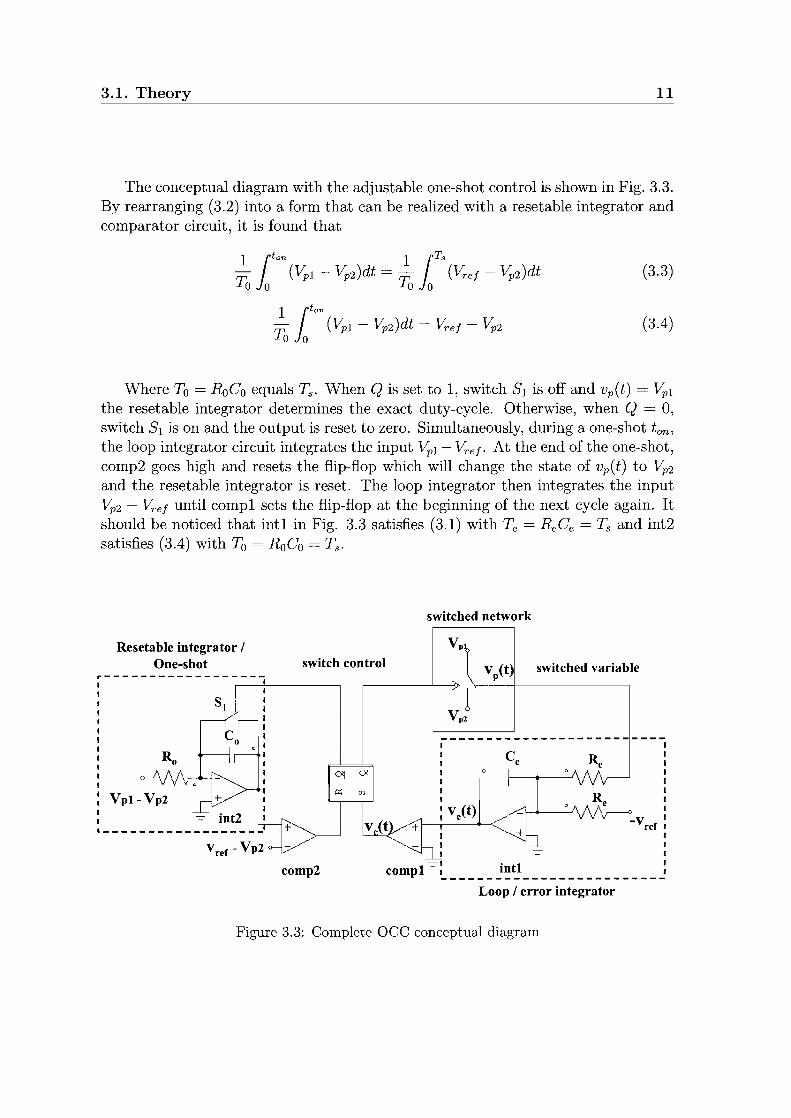
The conceptual diagram with the adjustable one-shot control is shown in Fig. 3.3.By rearranging (3.2) into a form that can be realized with a resetable integrator andcomparator circuit, it is found that
(3.3)
(3.4)
Where To = RaGo equals Ts . When Q is set to 1, switch 8 1 is off and vp(t) = ~1
the resetable integrator determines the exact duty-cycle. Otherwise, when Q = 0,switch 8 1 is on and the output is reset to zero. Simultaneously, during a one-shot ton,the loop integrator circuit integrates the input ~1 - Vref . At the end of the one-shot,comp2 goes high and resets the flip-flop which will change the state of vp(t) to ~2
and the resetable integrator is reset. The loop integrator then integrates the input~2 - ~ef until compl sets the flip-flop at the beginning of the next cycle again. Itshould be noticed that intI in Fig. 3.3 satisfies (3.1) with Te = ReGe = Ts and int2satisfies (3.4) with To = RoGo = Ts .
switched network
switch controlResetable integrator /
One-shot
V P1\ ~p(t
,--------+----4rV p2
switched variable
comp2 compl -~ !~~ 2
Loop / error integrator
Figure 3.3: Complete acc conceptual diagram
12 Chapter 3. Improved one-cycle control
3.2 Pulse width modulation, double-edge
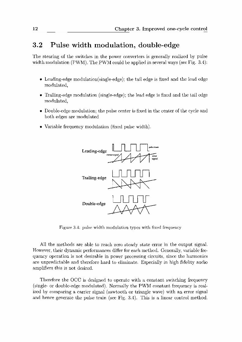
The stearing of the switches in the power converters is generally realized by pulsewidth modulation (PWM). The PWM could be applied in several ways (see Fig. 3.4):
• Leading-edge modulation(single-edge); the tail edge is fixed and the lead edgemodulated,
• Trailing-edge modulation (single-edge); the lead edge is fixed and the tail edgemodulated,
• Double-edge modulation; the pulse center is fixed in the center of the cycle andboth edges are modulated
• Variable frequency modulation (fixed pulse width).
~...uamLeading-edge
canicNdgn:Y1 /1~
~- V I signal
Trailing-edge~
LJUlJUDouble-edge~
Figure 3.4: pulse width modulation types with fixed frequency
All the methods are able to reach zero steady state error in the output signal.However, their dynamic performances differ for each method. Generally, variable frequency operation is not desirable in power processing circuits, since the harmonicsare unpredictable and therefore hard to eliminate. Especially in high fidelity audioamplifiers this is not desired.
Therefore the aee is designed to operate with a constant switching frequency(single- or double-edge modulated). Normally the PWM constant frequency is realized by comparing a carrier signal (sawtooth or triangle wave) with an error signaland hence generate the pulse train (see Fig. 3.4). This is a linear control method.
3.2. Pulse width modulation, double-edge 13
However in the aee technique the PWM is realized by comparing the control variable directly with its reference signal what gives the controller a non-linear character(see Fig. 2.2).
As discussed in the previous section the switching frequency in the improvedcontroller is determined by both the resetable one-shot integrator and the loop integrator. The resetable one-shot sets the on time ton and the loop integrator thendetermines the off time to!! such that the error is zero. In theory, when both thepower supply voltage (Vp1 and Y;2) and the reference control signal are constant andthe circuit is free of delays, the switching frequency is constant. But in practice thisis impossible and hence the switching frequency changes slightly.
In the conventional aee the switch is controlled single-edge leading modulationas shown in Fig. 2.2. However in the improved aee , the PWM is realized bydouble-edge modulation. Double-edge results in less switching frequency variation,which is preferable to achieve a lower distortion.In case of single-edge modulation, the center of the pulses is modulated by the perturbation around the average center, since one edge of the pulses is locked with clock(see Fig. 3.5). This introduces a perturbation frequency component at the outputspectrum, especially when the frequency is higher the effect becomes more severe.But, with double-edge modulation both sides are modulated while the center of thepulse is kept constant for each cycle (see Fig. 3.6). The pulse position modulationeffect should be eliminated. This effect is illustrated in Fig. 3.5 and 3.6
pul!ie centre
:~k~1I i-..I i
v, --1 iI iI iI d,T, I djT,+-.------+.
T,
,!/II v,
III
doT,
1
T,
,I d,T,
Figure 3.5: Pulse centre is modulated Figure 3.6: Pulse centre is fixed
The double-edge modulation could be realized by combining leading- and trailingedge modulation on alternate half cycles (see Fig. 3.7).
If the input supply voltages Vp1 and Y;2 and the reference voltage ~e! are allconstant then the switching frequency is also constant. A formula for the exact ontime ton to achieve constant switching frequency was derived in the previous section,equation(3.2). However, if the values for Y;l' Y;2' and ~e! are changing substan-
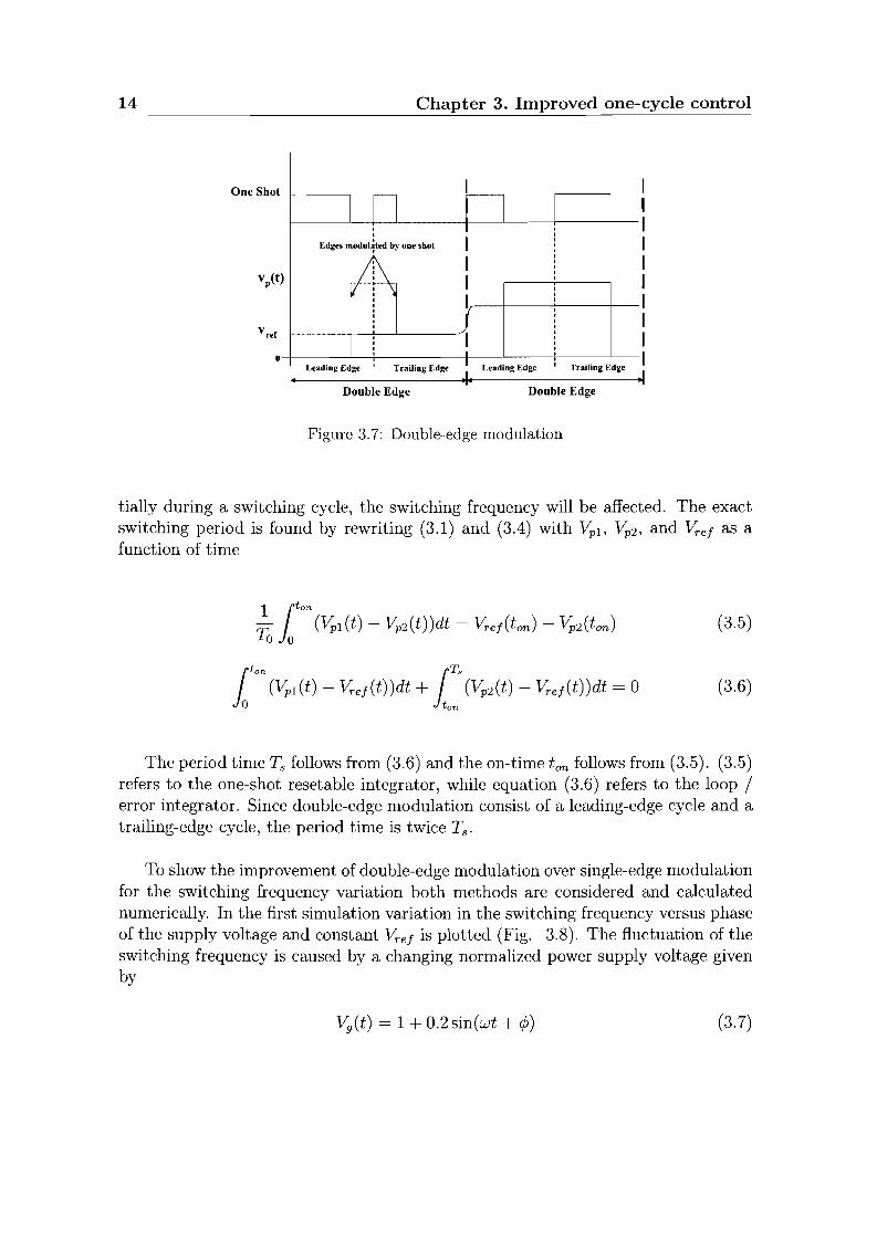
14 Chapter 3. Improved one-cycle control
One Shot 1--------,
,,,Edges modulated by oue shot
o-+-------'-----i--L------+---'----;-----'------
Double Edge Double Edge
Leadiug Edge Trailiug Edge Leading Edge
.1.Trailing Edge
.1
Figure 3.7: Double-edge modulation
tially during a switching cycle, the switching frequency will be affected. The exactswitching period is found by rewriting (3.1) and (3.4) with ~l, ~2, and ~ef as afunction of time
1 ronTo Jo (~l(t) - Vp2 (t))dt = ~ef(ton) - ~2(ton)
ron (~l(t) _ ~ef(t))dt + iTs (Vp2 (t) - ~ef(t))dt = 0Jo ton
(3.5)
(3.6)
The period time Ts follows from (3.6) and the on-time ton follows from (3.5). (3.5)refers to the one-shot resetable integrator, while equation (3.6) refers to the loop /error integrator. Since double-edge modulation consist of a leading-edge cycle and atrailing-edge cycle, the period time is twice Ts .
To show the improvement of double-edge modulation over single-edge modulationfor the switching frequency variation both methods are considered and calculatednumerically. In the first simulation variation in the switching frequency versus phaseof the supply voltage and constant ~ef is plotted (Fig. 3.8). The fluctuation of theswitching frequency is caused by a changing normalized power supply voltage givenby
Vg(t) = 1 + O.2sin(wt + ¢) (3.7)
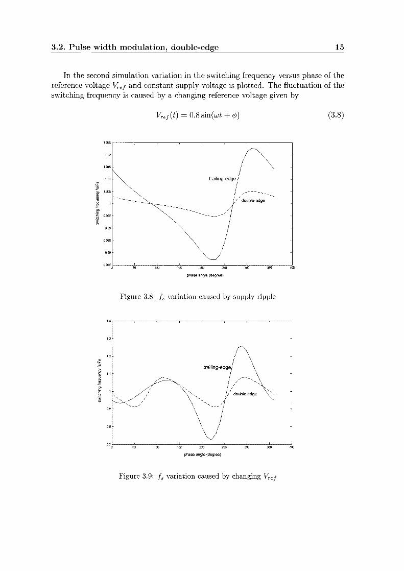
3.2. Pulse width modulation, double-edge 15
In the second simulation variation in the switching frequency versus phase of thereference voltage 1!;.ej and constant supply voltage is plotted. The fluctuation of theswitching frequency is caused by a changing reference voltage given by
Vrej(t) = O.8sin(wt + ¢)
phase angle (degree)
Figure 3.8: is variation caused by supply ripple
t,4 !
phase angle (degree)
Figure 3.9: is variation caused by changing Vrej
(3.8)
16 Chapter 3. Improved one-cycle control
Both Figures show clearly that double-edge modulation causes a considerablylower switching frequency fluctuation. When there is a 40% perturbation in the supply voltage the switching frequency fluctuation is ±2.25% and ±0.5% of the nominalvalue for trailing-edge and double-edge modulation respectively. The nominal switching frequency is is chosen 100 times greater than the supply voltage frequency. Whenthe reference voltage is changing in time this has larger influence on the switchingfrequency fluctuation. However, double-edge modulation shows much less is variation (±8%) compared to trailing-edge modulation (±27%). The nominal switchingfrequency is is chosen 10 times greater than the reference voltage frequency.
3.3 Improved one-cycle control circuit
Full bridge
" IE~ EJrv
Vg+- + Vp
-
~~ E~
-~
...... 0CI
9Vpl
Vp2ref.V ref '"'V
Improved OCC
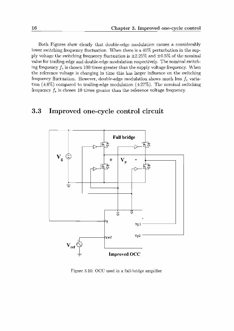
Figure 3.10: aee used in a full-bridge amplifier
3.3. Improved one-cycle control circuit 17
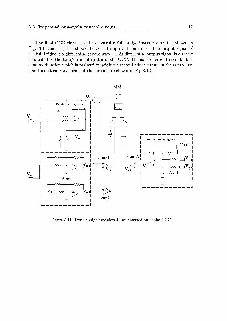
The final acc circuit used to control a full bridge inverter circuit is shown inFig. 3.10 and Fig 3.11 shows the actual improved controller. The output signal ofthe full-bridge is a differential square wave. This differential output signal is directlyconnected to the loop/error integrator of the acc. The control circuit uses doubleedge modulation which is realized by adding a second adder circuit in the controller.The theoretical waveforms of the circuit are shown in Fig.3.12.
~------------,
I Loop / error integrator II -Vref II II I
comp3l Vp1
:
I Ve . v\I'v-CJV P2:I' I
I I :I .::.. J
r- - Res~;:;: ::egr;:; ...,
I . II II II II II II I. V u II .ott I
: ~ Jr-----------. . II II I -------'''""-I ml
I II I
~------' I Adders II II II L-------c_"-.Vc2I m2 +
I ~ IIJ
V ref
Figure 3.11: Double-edge modulated implementation of the aee
18 Chapter 3. Improved one-cycle control
60.00 1~-:--:T----:1:~=====+==1=======;:::::;----:-I-1Vref \ip \
0.00 1'-0'="'="="=''..:.;;''==c:=J:====;.:=+===;-:.:.:.:.:\:====J=====.:;:=o.:.:.;:j="='-=--':':"-=---=-jI' \
-6000 C=======t=1======:t=== Lj............................. :======:t==1=====1LCllding-cdge (liLTs) Trailing-edge (li2Ts)
3.00 ,-------+----------+---~.-----,--+----,
_~~~ _~+==~:::; _ ~::-:::.,.~-1~..::.:c..'·~r~
:
01
-~~~ Vnll .:.. .. -~~:::.:.:-2.50 t::====~~====±:::="--==:::!===,==::j=====±=====±::==f====1
Vm2
1.00 ,------,/-------,------+-----.----------f------,
0.00 ~---~--+----~--'---~---I'--------'---'----~---/--~
1.00 ,----,---+----,----,------\-----,-------,----\------,
Vc3 VeL Vc1
0.00 L----~-t----......cJ-..l.L--~_f---->-..JlL----~__t---
Figure 3.12: Double-edge modulation theoretical waveforms
The circuit operates as follow:In one switching period four states can be distinguished. These four states are realized by the logic circuitry along with the outputs Vel, V c2, and V c3 of the comparators.
state 81 [to, td
The first state is started when the switching cycle starts at to when V c3 turnshigh. The resetable integrator starts a leading-edge modulated half cycle (see Fig.3.12). During this stage Q and QI are both low, Y;2 = Vg and Y;l = O. Theend of this state is reached when the resetable integrator reaches the reference levelVm2 = -(Vg - Vrej ) , the comp2 goes high and Q and QI change both to high.
This state is started at t l . During this second state the resetable integrator isreset and remains O. Now Vp2 = 0 and Y;l = Vg as Q and QI both changed from lowto high. The loop / error integrator integrates until it reaches zero at t 2 and comp3becomes zero. The first half cycle is then ended and the next state is started.
3.3. Improved one-cycle control circuit 19
At t 2 the third state is started and the resetable integrator is triggered again tostart a trailing-edge half cycle. This time Q remains high and Ql has changed tolow. Thus the error integrator keeps integrating in the same direction. The end ofthis state is reached when the resetable integrator reaches the second reference levelVm1 = -(Vg + ~ef) at t3 and compl goes high and triggers to the last state in thecycle.
During this last state Q and Ql both change to low and high respectively. ~2 =Vg and ~l = O. The resetable integrator is kept zero and the error integratorintegrates until it reaches zero again at t4 . Then the end of the second half cycle isreached and the whole operation is repeated cycle by cycle.
3.3.1 Resetable integrator
Fig. 3.13 shows the implementation of the resetable integrator. It is a so-calledHowland current source with an additional capacitor. If the integrator is configuredproperly, a constant current, which is independent of the capacitor voltage, flowsthrough the capacitor. As a result a precise linear voltage ramp can be generated.
R3
C3§J---/\AfL ·-----.--I
supply voltage R2INT2
R4
,----+-------j Vu
integrated voltage~--\ Cl
LIFigure 3.13: Resetable integrator circuit
20 Chapter 3. Improved one-cycle control
Additionally, the integrator needs to reset every time the reference level is reached.When the duty-cycle ratio approaches unity, a slow reset time could cause the controller to work improper, for high switching frequencies.
The switching frequency is determined by both the slope of the voltage outputramp of the resetable integrator and the reference voltage level at which the integrator needs to be resetted. From Fig. 3.14 it follows that if the slope of the outputvoltage ramp Vu is changed, the switching time Ts changes simultaneously. Additionally, if the reference voltage level Vm1 or Vm2 (see Fig. 3.11) is adapted, it influencesthe time Ts too. Concluding, the switching time Ts can be changed by:
• Changing the current through the capacitor, by changing the resistors valuesof the resetable integrator
• Changing the value of the capacitor C1.
• Changing the reference voltage level Vm1 or Vm2 .
0,
-4.5 r --j----__-+__--! +-'V'-"'m!.'-'11r=ef=e,-,;re""nc=e-,-v=ol=ta"9QE
-5 OL-----'-------'------'3.---4-'-.-----="---6
.' I ~.. Time(s) x 10One shollime
Figure 3.14: Resetable integrator output voltage (R1 = R2 = 1kw, R3 = R4 =
200wVg = 70 + 5 * sin(w * t))
Furthermore, the resetable integrator needs to be dimensioned such that for themaximum supply voltage Vg the voltage ramp Vu is kept beneath the saturation voltage of the op-amp. Additionally, a low maximum voltage Vu is advantageous to havea fast resetting of the capacitor.
When the switch is turned on the capacitor is short-circuited and Vu (voltageacross the capacitor) becomes zero (reset). During switch off, the capacitor is loadeduntil it reaches its reference voltage level. The integrator can then be simplifiedaccording to Fig. 3.15.
3.3. Improved one-cycle control circuit 21
R2
supply voltage
-(R4*Rl/R3)I a - Jt,
> I< ·VV'v--II.Ie .
IFigure 3.15: Simplified current model
The current through the capacitor is given by
(3.9)
(3.10)
So if R2 = R4R11R3, then the current into the capacitor depends only on theinput voltage Vg and R2
I __ Vgc - R
2
and if the input voltage is not constant the capacitor output voltage is then
1 it. 1 it V 9 ( t ) -1 itvu(t) = -0 ~c(t)dt = -0 --dt = 0 R vg(t)dt1 0 1 0 R2 1 2 0
(3.11)
If the supply voltage is assumed to be constant then the output capacitor voltageis given by
(3.12)
Switching duty-ratio
From the analysis above the limitations of the duty-ratio can be easily calculated.In theory the duty-ratio has a physical limitation that is 0 < d < 1. However, inpractice the duty-cycle is more limited due to for example switch onl off times orlimitations which are the result of the controller. Therefore the duty-ratio limits are
22 Chapter 3. Improved one-cycle control
Dmin < d < Dmax (3.13)
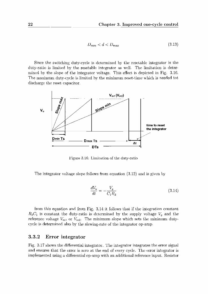
Since the switching duty-cycle is determined by the resetable integrator is theduty-ratio is limited by the resetable integrator as well. The limitation is determined by the slope of the integrator voltage. This effect is depicted in Fig. 3.16.The maximum duty-cycle is limited by the minimum reset-time which is needed totdischarge the reset capacitor.
time to resetthe integrator
AtDmin Ts....------ 0 max Ts
Vm1 (Vm2)-------~- ---------------------- ------------------------------- --------- ---
~ .~CZI '«\,...~ e~ S\O(I,)
DTs
Figure 3.16: Limitation of the duty-ratio
The integrator voltage slope follows from equation (3.12) and is given by
(3.14)
from this equation and from Fig. 3.14 it follows that if the integration constantR2C1 is constant the duty-ratio is determined by the supply voltage Vg and thereference voltage Vm1 or Vm2 . The minimum slope which sets the minimum dutycycle is determined also by the slewing-rate of the integrator op-amp.
3.3.2 Error integrator
Fig. 3.17 shows the differential integrator. The integrator integrates the error signaland ensures that the error is zero at the end of every cycle. The error integrator isimplemented using a differential op-amp with an additional reference input. Resistor
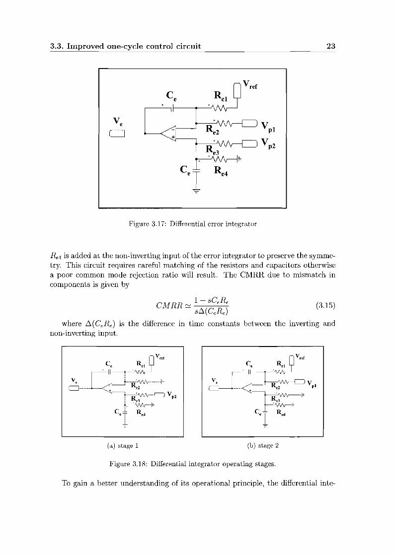
3.3. Improved one-cycle control circuit 23
+
V ref
Re2
v'\--C) Vpl
R ~Vp2e3
-~. '/\Jv----1I'Re4
Figure 3.17: Differential error integrator
Re4 is added at the non-inverting input ofthe error integrator to preserve the symmetry. This circuit requires careful matching of the resistors and capacitors otherwisea poor common mode rejection ratio will result. The CMRR due to mismatch incomponents is given by
(3.15)
where ~(CeRe) is the difference in time constants between the inverting andnon-inverting input.
(a) stage 1 (b) stage 2
Figure 3.18: Differential integrator operating stages.
To gain a better understanding of its operational principle, the differential inte-
24 Chapter 3. Improved one-cycle control
grator can be split up in two stages. In the first stage, Fig. 3.18(a),"V;1 is connectedto earth and "V;2 is high. In the second stage Fig. 3.18(b) "V;2 is connected to earthand "V;I is high. Since the switching frequency is high we can assume that the inputvoltage V; is constant during one switching cycle. Therefore we can write the following equations for stage 1 and stage 2 respectively
=? ~(stagel) = (1 + ZCe ) ( ZCe/ / Re4
) "V;2TonRed / R e2 ZCe/ / R e4 + R e3
=? ~(stage2) =
(3.16)
+ (1 + ZCe ) ( ZCe/ / R e3 ) 11: TRed / R e2 ZCe/ / R e3 + R e4 ref on
(1 + Zce) ( ZCe/ / R e3 ) 11: T
ReI ZCe/ / R e3 + R e4 ref off
with ZCe = -cls e
The summation of the two gives an expression for the error voltage during onehalf of the cycle. (leading or trailing-edge)
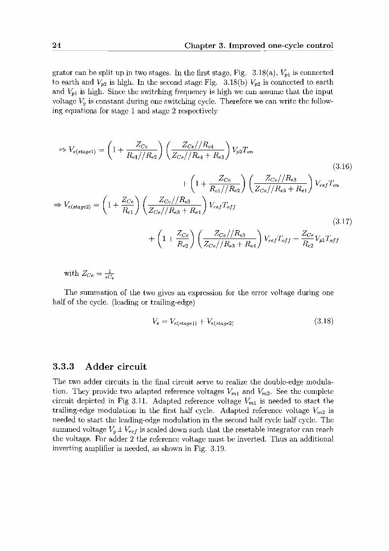
3.3.3 Adder circuit
~ = Ve(stagel) + ~(stage2) (3.18)
The two adder circuits in the final circuit serve to realize the double-edge modulation. They provide two adapted reference voltages Vml and Vm2 . See the completecircuit depicted in Fig 3.11. Adapted reference voltage Vml is needed to start thetrailing-edge modulation in the first half cycle. Adapted reference voltage Vm2 isneeded to start the leading-edge modulation in the second half cycle half cycle. Thesummed voltage V; ± "V:-ef is scaled down such that the resetable integrator can reachthe voltage. For adder 2 the reference voltage must be inverted. Thus an additionalinverting amplifier is needed, as shown in Fig. 3.19.
3.4. Sensitivity of the controller 25
supply voltage
Vg Ral Ra3
Ra2
Figure 3.19: Adder circuit
3.4 Sensitivity of the controller
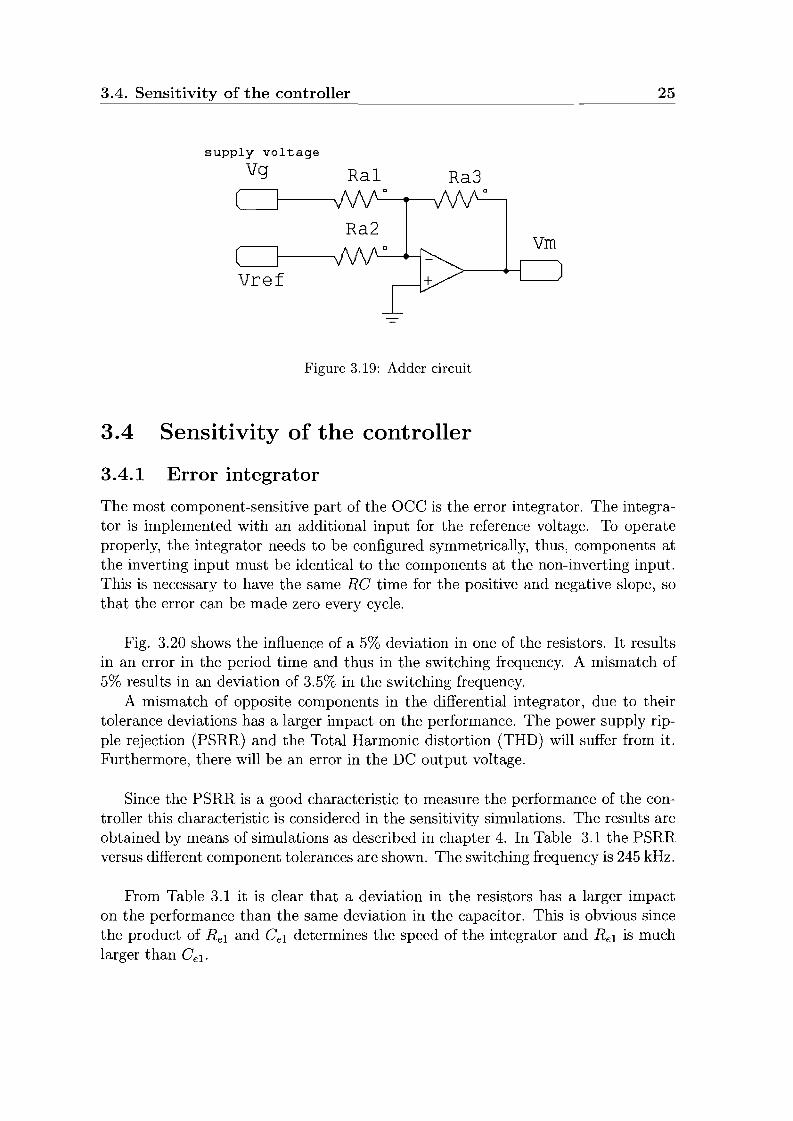
3.4.1 Error integrator
Vm
The most component-sensitive part of the acc is the error integrator. The integrator is implemented with an additional input for the reference voltage. To operateproperly, the integrator needs to be configured symmetrically, thus, components atthe inverting input must be identical to the components at the non-inverting input.This is necessary to have the same RG time for the positive and negative slope, sothat the error can be made zero every cycle.
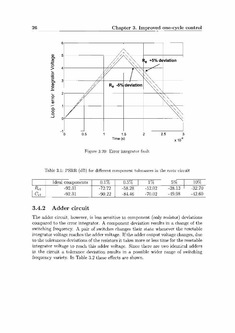
Fig. 3.20 shows the influence of a 5% deviation in one of the resistors. It resultsin an error in the period time and thus in the switching frequency. A mismatch of5% results in an deviation of 3.5% in the switching frequency.
A mismatch of opposite components in the differential integrator, due to theirtolerance deviations has a larger impact on the performance. The power supply ripple rejection (PSRR) and the Total Harmonic distortion (THD) will suffer from it.Furthermore, there will be an error in the DC output voltage.
Since the PSRR is a good characteristic to measure the performance of the controller this characteristic is considered in the sensitivity simulations. The results areobtained by means of simulations as described in chapter 4. In Table 3.1 the PSRRversus different component tolerances are shown. The switching frequency is 245 kHz.
From Table 3.1 it is clear that a deviation in the resistors has a larger impacton the performance than the same deviation in the capacitor. This is obvious sincethe product of ReI and Gel determines the speed of the integrator and ReI is muchlarger than Gel.
26 Chapter 3. Improved one-cycle control
a>Olctl-o>L-
o-~Ola>-cL-
eL-
a>-c.oo
...J
6
5
4
3
2
o
// ~.."~fYI~ I
~ +5%deviation,,"'",,"" /"
~ !~,/
/ ~""/// ""W Re ·5°/c deviation ~~,~1y '\ '"f \"'"/J
"'\~",#
1/ ~-1
o 0.5 1.5Time (5)
2 2.5 3
x10~
Figure 3.20: Error integrator fault
Table 3.1: PSRR (dB) for different component tolerances in the error circuit
Ideal components 0.1% 0.5% 1% 5% 10%ReI -92.31 -72.72 -58.28 -52.02 -38.13 -32.70Gel -92.31 -90.22 -84.46 -70.02 -49.98 -42.60
3.4.2 Adder circuit
The adder circuit, however, is less sensitive to component (only resistor) deviationscompared to the error integrator. A component deviation results in a change of theswitching frequency. A pair of switches changes their state whenever the resetableintegrator voltage reaches the adder voltage. If the adder output voltage changes, dueto the tolerances deviations of the resistors it takes more or less time for the resetableintegrator voltage to reach this adder voltage. Since there are two identical addersin the circuit a tolerance deviation results in a possible wider range of switchingfrequency variety. In Table 3.2 these effects are shown.
3.5. Delay time and its impact on the performance
Table 3.2: PSRR (dB) for different component tolerances in the adder circuit
27
Ideal components 0.1% 0.5% 1% 5% 10%Ra1 -92.31 -90.05 -83.21 -86.94 -73.45 -67.83
3.4.3 Resetable Integrator
A deviation in the component value in the resetable integrator has the least impacton the performance of the circuit. Since the resetable integrator operates in itslinear region a value deviation results in a slight change in the sloop of the integratorand therefore, a small change in the switching frequency. Except the change inperformance of the controller due to the change in switching frequency the componentvalue deviation has no other influence on the performance.
Table 3.3: PSRR (dB) for different component tolerances
Ideal components 5% 10%R1 -92.31 -86,00 -82.93R2 -92.31 -84,00 -77.03
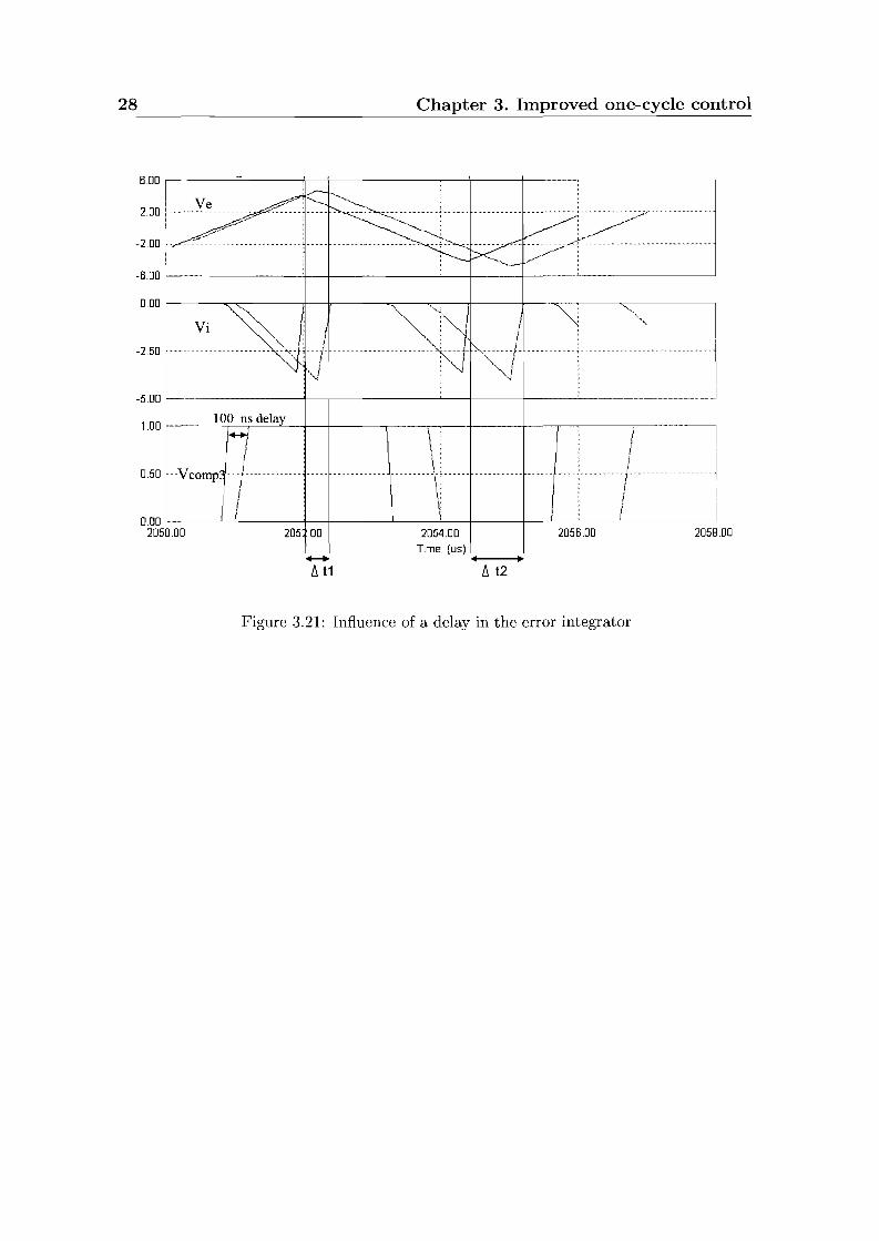
3.5 Delay time and its impact on the performance
Delay time in the control circuit directly influences the switching frequency and indirectly decreases the performance. The delays occur for example when the resetableintegrator completes its one-shot (ton) to reset the flip-flop which changes on its turnthe state of the input signal ~. This is depicted in Fig. 3.21 as ~t1. Thus fromthe moment that the one shot completes, it takes a small delay before the errorintegrator really changes its integration direction. Depending on the slopes of theerror integrator this can have a relative small or large effect on the period time. Thiseffect is depicted in Fig 3.21 as ~t2
The same effect can occur at the moment the error integrator equals zero andsets both the flip-flop to change the state of the bridge voltage and the resetable integrator to start integrating. As mentioned before these delays influence the switchingfrequency, by decreasing it. However, despite these delays the controller can stilloperate correctly but only with a lower switching frequency. To compensate thesedelays a small resistor can be added in the resetable integrator in series with C1 tomake the one-shot slightly faster. Another solution is by simply increasing the frequency by choosing a smaller capacitor for instance. In the next chapter the impacton the PSRR caused by time-delays is quantified.
28 Chapter 3. Improved one-cycle control
2.00
-6.00
-2.00
6.00 ,---------==--------+-----4--------+----+----------_:~~ : :
y'~G~···················7~. ··~···················:·················~><:~1·········· .
2058.002056.002054.00
Time (us) ..--.1I 12
205 .00
-5.00 '---------+-+--------'--+-----1----'--------
1 DO ._ 100 TIS delayn \.- f---..- /
0.50 ·Vcomp- I········· , \\., , ······'10.00 '--__'--'- -+--+ -'----_---'_-+-__--1----'_-'-_----"- _
2050.00
Figure 3.21: Influence of a delay in the error integrator
Chapter 4
Simulations
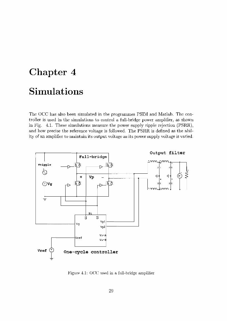
The ace has also been simulated in the programmes PSIM and Matlab. The controller is used in the simulations to control a full-bridge power amplifier, as shownin Fig. 4.1. These simulations measure the power supply ripple rejection (PSRR),and how precise the reference voltage is followed. The PSRR is defined as the ability of an amplifier to maintain its output voltage as its power supply voltage is varied.
I1ri ple
51
Output filter
'----------1 Vg
Mo
Mo
Vpll--------'
vpZI---------'
One-cycle controllerVref
,--------iVr"fVo
Vo-
Figure 4.1: aee used in a full-bridge amplifier
29
30 Chapter 4. Simulations
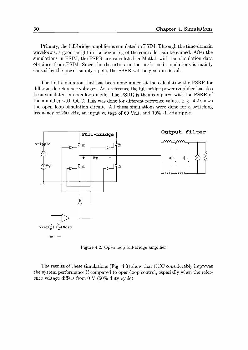
Primary, the full-bridge amplifier is simulated in PSIM. Through the time-domainwaveforms, a good insight in the operating of the controller can be gained. After thesimulations in PSIM, the PSRR are calculated in Matlab with the simulation dataobtained from PSIM. Since the distortion in the performed simulations is mainlycaused by the power supply ripple, the PSRR will be given in detail.
The first simulation that has been done aimed at the calculating the PSRR fordifferent dc reference voltages. As a reference the full-bridge power amplifier has alsobeen simulated in open-loop mode. The PSRR is then compared with the PSRR ofthe amplifier with acc. This was done for different reference values. Fig. 4.2 showsthe open loop simulation circuit. All these simulations were done for a switchingfrequency of 250 kHz, an input voltage of 60 Volt, and 10% -1 kHz ripple.
FUll-bridge
Vp
output filter
Figure 4.2: Open loop full-bridge amplifier
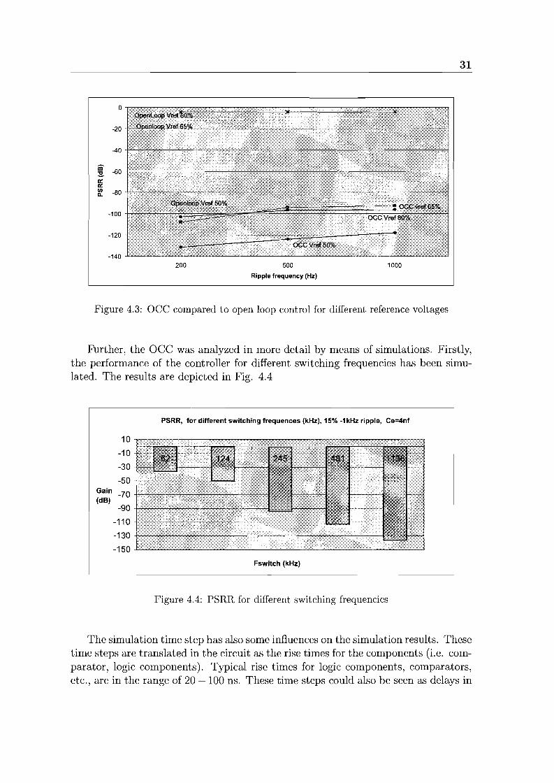
The results of these simulations (Fig. 4.3) show that acc considerably improvesthe system performance if compared to open-loop control, especially when the reference voltage differs from 0 V (50% duty cycle).
31
0
-20
-40
iii -60~0::0::VI -80n.
-100
-120
-140200 500
Ripple frequency (Hz)
1000
Figure 4.3: acc compared to open loop control for different reference voltages
Further, the aee was analyzed in more detail by means of simulations. Firstly,the performance of the controller for different switching frequencies has been simulated. The results are depicted in Fig. 4.4
PSRR, for different switching frequences (kHz), 15% -1 kHz ripple, Ce=4nf
Gain(dB)
10
-10
-30
-50
-70
-90
-110
-130
-150
Fswitch (kHz)
Figure 4.4: PSRR for different switching frequencies
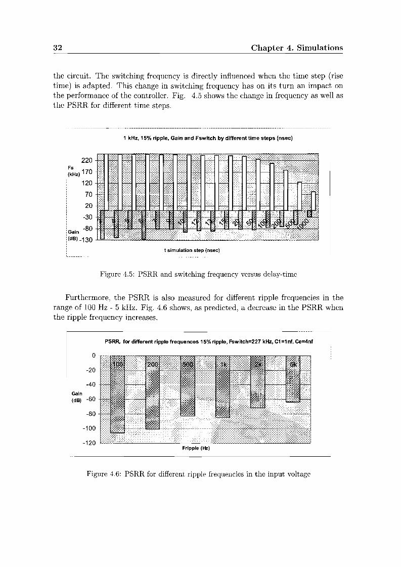
The simulation time step has also some influences on the simulation results. Thesetime steps are translated in the circuit as the rise times for the components (i.e. comparator, logic components). Typical rise times for logic components, comparators,etc., are in the range of 20 - 100 ns. These time steps could also be seen as delays in
32 Chapter 4. Simulations
the circuit. The switching frequency is directly influenced when the time step (risetime) is adapted. This change in switching frequency has on its turn an impact onthe performance of the controller. Fig. 4.5 shows the change in frequency as well asthe PSRR for different time steps.
1 kHz, 15% ripple, Gain and Fswitch by different time steps (nsec)
220Fs(kHz) 170
120
70
20
-30
-80Gain
(dB) -130
t simulation step (nsec)
Figure 4.5: PSRR and switching frequency versus delay-time
Furthermore, the PSRR is also measured for different ripple frequencies in therange of 100 Hz - 5 kHz. Fig. 4.6 shows, as predicted, a decrease in the PSRR whenthe ripple frequency increases.
PSRR, for different ripple frequences 15% ripple, Fswitch=227 kHz, C1 =1 nf, Ce=4nf
o
-20
-40
Gain(dB) -60
-100
-120Fripple (Hz)
Figure 4.6: PSRR for different ripple frequencies in the input voltage

33
In conclusion, the aee has shown good performances concerning the power supply ripple rejection. This was in accordance with the expectation. Since the maincharacteristics of the aee is its ability to reject power supply disturbance. Further, simulations have shown that the switching frequency plays also a role in theperformances of the aee. The higher the switching frequency the better the aeeperforms if the power-stage behaves ideal. The power supply ripple frequency hasalso some influence on the performance. As the frequency of the ripple is lower thanthe controller rejects this ripple better as expected.
Chapter 5
Practical Implementation
5.1 Controller implementation
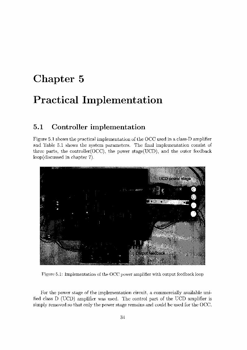
Figure 5.1 shows the practical implementation ofthe OCC used in a class-D amplifierand Table 5.1 shows the system parameters. The final implementation consist ofthree parts, the controller(OCC), the power stage(UCD), and the outer feedbackloop (discussed in chapter 7).
Figure 5.1: Implementation of the aee power amplifier with output feedback loop
For the power stage of the implementation circuit, a commercially available unified class D (UCD) amplifier was used. The control part of the UCD amplifier issimply removed so that only the power stage remains and could be used for the OCC.
34
5.1. Controller implementation 35
The results of the OCC amplifier are then compared with the performances of theself-oscillating UCD power amplifier.
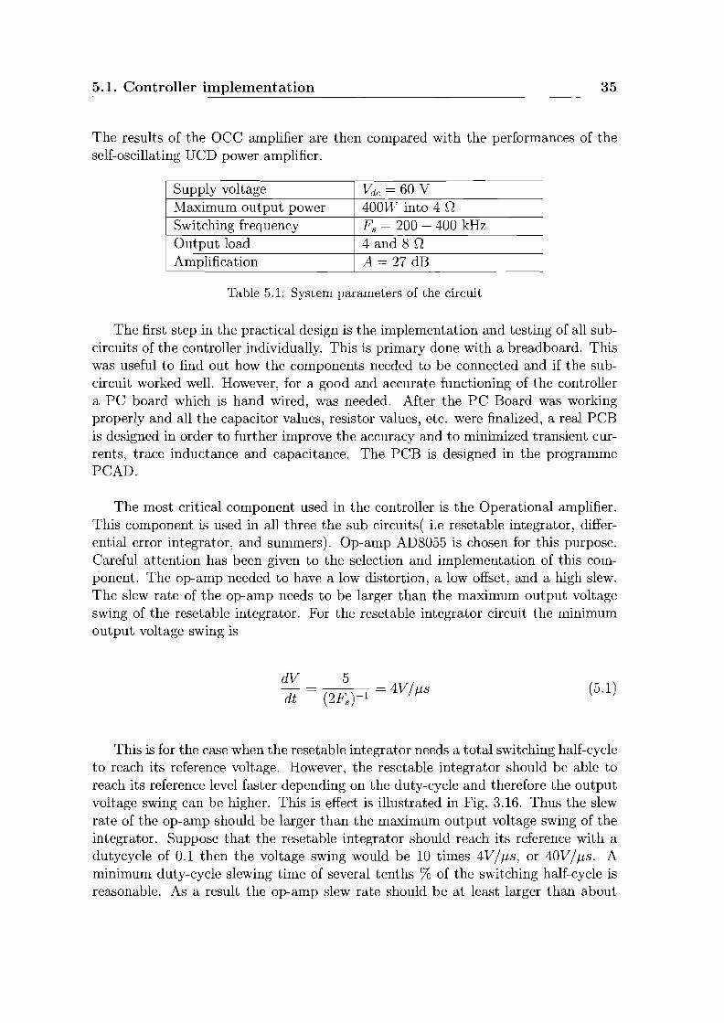
Supply voltage Vdc = 60 VMaximum output power 400W into 4 [2
Switching frequency Fs = 200 - 400 kHzOutput load 4 and 8 [2
Amplification A = 27 dB
Table 5.1: System parameters of the circuit
The first step in the practical design is the implementation and testing of all subcircuits of the controller individually. This is primary done with a breadboard. Thiswas useful to find out how the components needed to be connected and if the subcircuit worked well. However, for a good and accurate functioning of the controllera PC board which is hand wired, was needed. After the PC Board was workingproperly and all the capacitor values, resistor values, etc. were finalized, a real PCBis designed in order to further improve the accuracy and to minimized transient currents, trace inductance and capacitance. The PCB is designed in the programmePCAD.
The most critical component used in the controller is the Operational amplifier.This component is used in all three the sub circuits( i.e resetable integrator, differential error integrator, and summers). Op-amp AD8055 is chosen for this purpose.Careful attention has been given to the selection and implementation of this component. The op-amp needed to have a low distortion, a low offset, and a high slew.The slew rate of the op-amp needs to be larger than the maximum output voltageswing of the resetable integrator. For the resetable integrator circuit the minimumoutput voltage swing is
dV
dt(5.1)
This is for the case when the resetable integrator needs a total switching half-cycleto reach its reference voltage. However, the resetable integrator should be able toreach its reference level faster depending on the duty-cycle and therefore the outputvoltage swing can be higher. This is effect is illustrated in Fig. 3.16. Thus the slewrate of the op-amp should be larger than the maximum output voltage swing of theintegrator. Suppose that the resetable integrator should reach its reference with adutycycle of 0.1 then the voltage swing would be 10 times 4V//-Ls, or 40V//-Ls. Aminimum duty-cycle slewing time of several tenths % of the switching half-cycle isreasonable. As a result the op-amp slew rate should be at least larger than about
36
SR > 100V/ JIB
Chapter 5. Practical Implementation
To reset the integrator an analog multiplexer 74HC4052 is used. The device isan high speed switch with low" on" resistance and low" off" leakage. For the logiccircuitry, logic gates from the HEF series are used. And for the comparator the opamp LM319 is chosen. These components were tested and found to be suited to beused in the controller. In appendix A a complete implementation scheme is added.
5.2 Time domain signal measurement
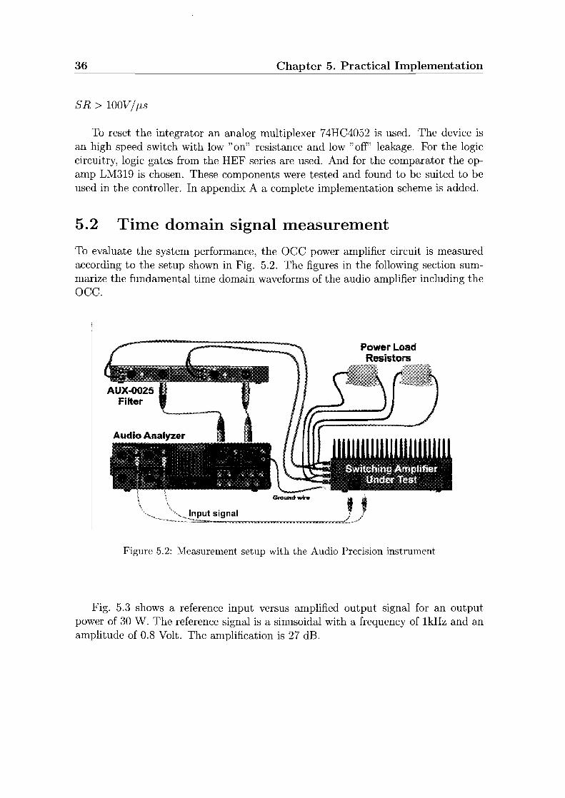
To evaluate the system performance, the acc power amplifier circuit is measuredaccording to the setup shown in Fig. 5.2. The figures in the following section summarize the fundamental time domain waveforms of the audio amplifier including theacc.
,""~'_~_ \'''~ut signal-_ =.~.=~~__=.."'="'.. = ~=.x.=__~
Figure 5.2: Measurement setup with the Audio Precision instrument
Fig. 5.3 shows a reference input versus amplified output signal for an outputpower of 30 W. The reference signal is a sinusoidal with a frequency of 1kHz and anamplitude of 0.8 Volt. The amplification is 27 dB.
5.2. Time domain signal measurement
Channel 1399JJ() tlCDO.C:
199JJ(]
99JII
iXlJmV
mUll
·20i,OO
401.00 4000 C'
500 IoU:IOI''r'
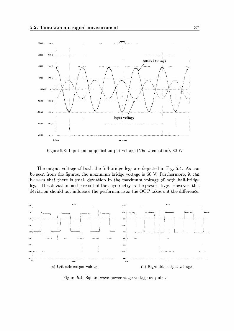
Figure 5.3: Input and amplified output voltage (50x attenuation), 30 W
37
The output voltage of both the full-bridge legs are depicted in Fig. 5.4. As canbe seen from the figures, the maximum bridge voltage is 60 V. Furthermore, it canbe seen that there is small deviation in the maximum voltage of both half-bridgelegs. This deviation is the result of the asymmetry in the power-stage. However, thisdeviation should not influence the performance as the acc takes out the difference.
(a) Left side output voltage (b) Right side output voltage
Figure 5.4: Square wave power stage voltage outputs.
38 Chapter 5. Practical Implementation
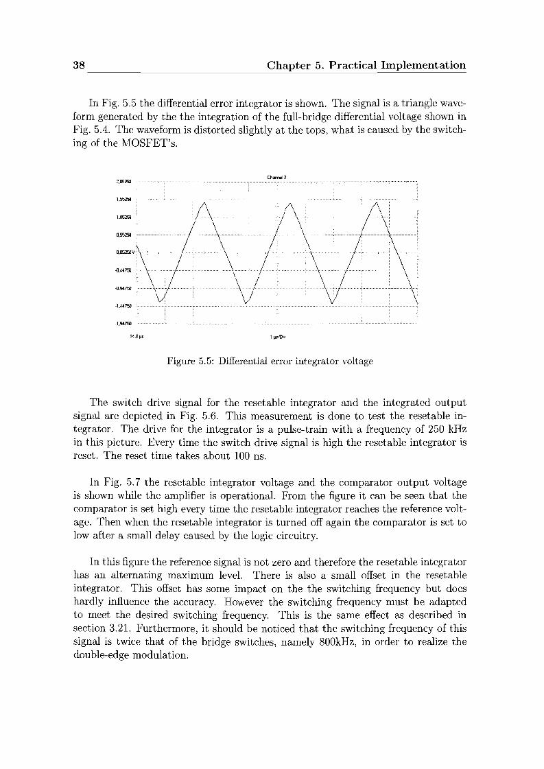
In Fig. 5.5 the differential error integrator is shown. The signal is a triangle waveform generated by the the integration of the full-bridge differential voltage shown inFig. 5.4. The waveform is distorted slightly at the tops, what is caused by the switching of the MOSFET's.
Figure 5.5: Differential error integrator voltage
The switch drive signal for the resetable integrator and the integrated outputsignal are depicted in Fig. 5.6. This measurement is done to test the resetable integrator. The drive for the integrator is a pulse-train with a frequency of 250 kHzin this picture. Every time the switch drive signal is high the resetable integrator isreset. The reset time takes about 100 ns.
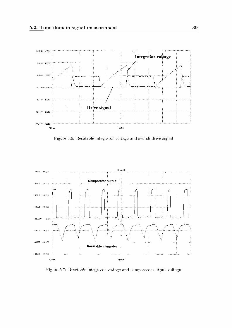
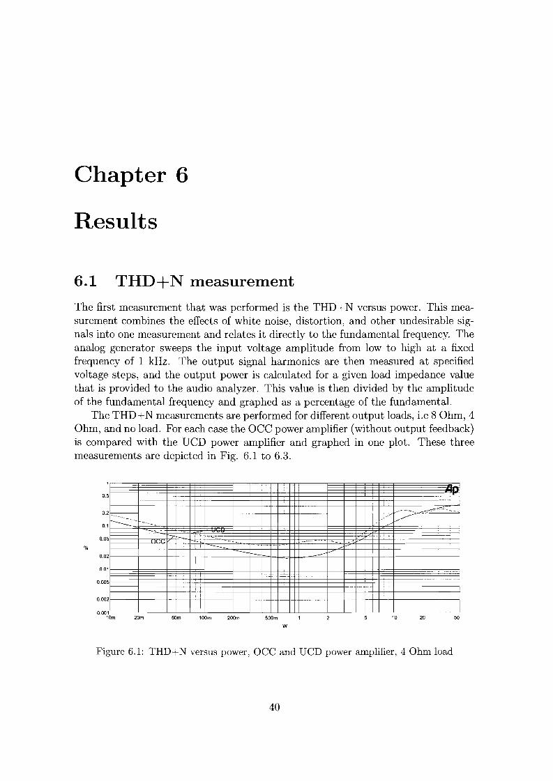
In Fig. 5.7 the resetable integrator voltage and the comparator output voltageis shown while the amplifier is operational. From the figure it can be seen that thecomparator is set high every time the resetable integrator reaches the reference voltage. Then when the resetable integrator is turned off again the comparator is set tolow after a small delay caused by the logic circuitry.
In this figure the reference signal is not zero and therefore the resetable integratorhas an alternating maximum level. There is also a small offset in the resetableintegrator. This offset has some impact on the the switching frequency but doeshardly influence the accuracy. However the switching frequency must be adaptedto meet the desired switching frequency. This is the same effect as described insection 3.21. Furthermore, it should be noticed that the switching frequency of thissignal is twice that of the bridge switches, namely 800kHz, in order to realize thedouble-edge modulation.
5.2. Time domain signal measurement 39
.10.1750 ·2)]250 c .
Dr . nal
9.B2s0 1 ,,50 •............ . .
14.B250 25'50
4.8250 u.S'50
·15.17~O ·JW=51J
1••1 ~. 1jlSA).Y
Figure 5.6: Resetable integrator voltage and switch drive signal
Charr1el17.9800 20iJO.OO
Resetable integrator
5,9800 , ~~[;UlO
3,9800 , QOG/iO
1,9900 ~OOJ:O
·0.02DOV
-2.0200 5UlUJD
-4.0200 -1800 CiO
, InlOrv
Figure 5.7: Resetable integrator voltage and comparator output voltage
Chapter 6
Results
6.1 THD+N measurement
The first measurement that was performed is the THD+N versus power. This measurement combines the effects of white noise, distortion, and other undesirable signals into one measurement and relates it directly to the fundamental frequency. Theanalog generator sweeps the input voltage amplitude from low to high at a fixedfrequency of 1 kHz. The output signal harmonics are then measured at specifiedvoltage steps, and the output power is calculated for a given load impedance valuethat is provided to the audio analyzer. This value is then divided by the amplitudeof the fundamental frequency and graphed as a percentage of the fundamental.
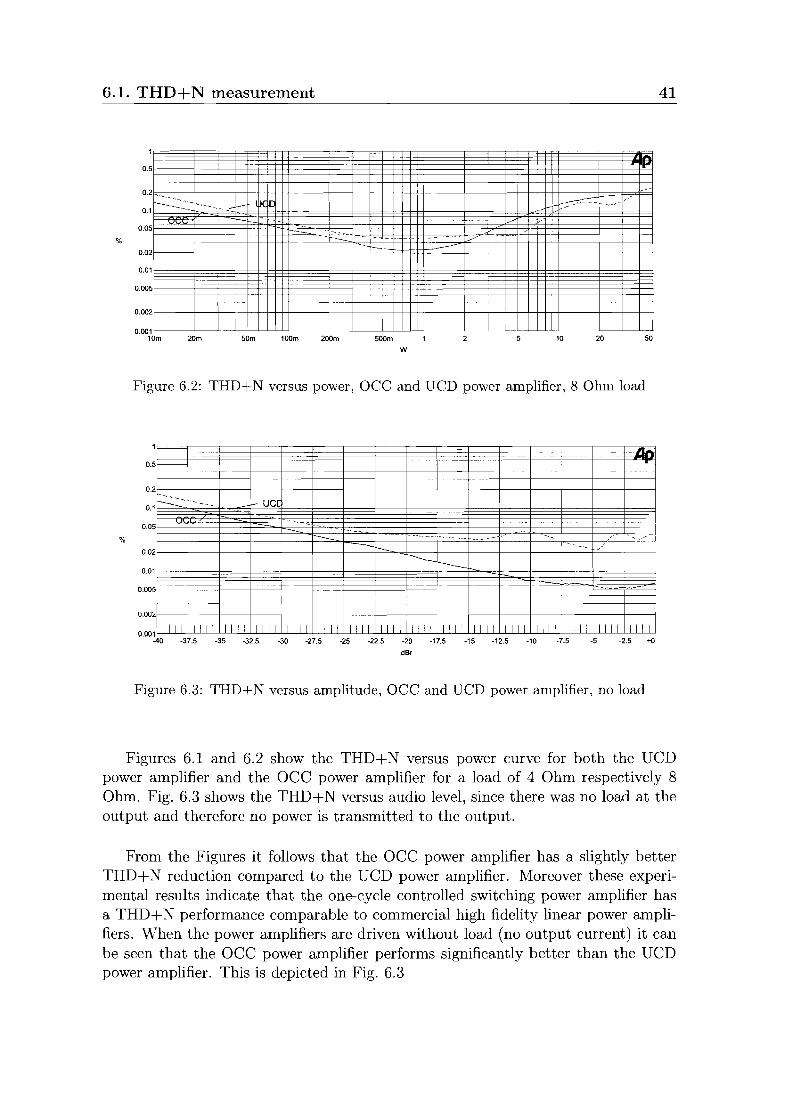
The THD+N measurements are performed for different output loads, i.e 8 Ohm, 4Ohm, and no load. For each case the OCC power amplifier (without output feedback)is compared with the UCD power amplifier and graphed in one plot. These threemeasurements are depicted in Fig. 6.1 to 6.3.
%
O,02r--+_+_+-++t+++--__+_-~__t=r-:=::::t=_t_I~=!+---=o-:::::__r-+_H__+_++H_-_+-+_+_I
O'01~__ft__O,005
RO,002r----+-___+___+--+~+++__-__+_-I___+_+_+_H_++_-_+-+__+__1_+_++t_+_-___+-+__+__I
w
Figure 6.1: THD+N versus power, OCC and UCD power amplifier, 4 Ohm load
40
6.1. THD+N measurement 41
%
0.02
0.01
0.005
0.002
0.00110m 20m
L-- Je
50m
- ---
100m 200m 500m
w10 20 50
Figure 6.2: THD+N versus power, OCC and UCD power amplifier, 8 Ohm load
1
~" '---._-., - UC[1'''.
".,- "'.~~_-~ -
----... ~.~~ ..._~ -.. , -~~ --- - - """
. ..,--r--. -- .-
--------............-.1
1 I II I 1111 II II I II I III I II II IIII III I I111 1111 II I I I III III I I III IIII I II I
0.02
0.2
o.
0.0
0.5
0.05
0.00-40 -37.5 -35 -32.5 ·30 -27.5 -25 ·22.5 ·20 ·17.5 -15 -12.5 -10 -7.5 -5 -2.5 +0
dBr
0.005
0.002
%
Figure 6.3: THD+N versus amplitude, OCC and UCD power amplifier, no load
Figures 6.1 and 6.2 show the THD+N versus power curve for both the UCDpower amplifier and the OCC power amplifier for a load of 4 Ohm respectively 8Ohm. Fig. 6.3 shows the THD+N versus audio level, since there was no load at theoutput and therefore no power is transmitted to the output.
From the Figures it follows that the OCC power amplifier has a slightly betterTHD+N reduction compared to the UCD power amplifier. Moreover these experimental results indicate that the one-cycle controlled switching power amplifier hasa THD+N performance comparable to commercial high fidelity linear power amplifiers. When the power amplifiers are driven without load (no output current) it canbe seen that the OCC power amplifier performs significantly better than the UCDpower amplifier. This is depicted in Fig. 6.3
42 Chapter 6. Results
The higher distortion of both power amplifiers at low output power is due to thedecrease in signal-to-noise ratio caused by the fixed noise floor. The measurementsuffers also from some typical low frequent noise as will be clear in the FFT plots inthe next section. In the design of the oee and the implementation with the powerstage not much attention is paid to signal routing. An improvement on this canresult in a better performance.
Furthermore, it should be noticed that the THD+N increases also when the powerincreases. This could be caused by imperfection in the power stage such as:
1. The main cause of the nonlinearity in the power stage is the timing errorsadded by the gate drivers, such as dead-time and on/off-time. Especially the errordue to the dead-time can affect the THD+N significantly when the power increases.During dead-time load current commutates through the MOSFET body diodes. Thediode conduction during these dead times leads to a duty cycle error at the outputof the power stage. This duty-cycle error increase when the modulation depth increases. Therefore the distortion will be larger with the increase of power.
2. Another cause is the presence of undesired characteristics in the switchingdevices, such as finite ON resistance, finite switching speed and ringing on transientedges.
3. Another cause is the non-linearity in the output low-pass filter. Since in themeasurements there is no output feedback and therefore disturbance in the outputare not rejected.
+35f---+---+--+-+-+-++++----+-f-r-+++++-f---+--+-+-+-+-++++----+-f-f-+++++loccVI\
+301----+-----+---+-+-+-+++t---f--+---t-+-++-++f-----+-----+--+-+-+-+++t---f--b"--f---+*-i-+H1-•••••••••••••••••••••••..•••••••••••••••••• , . ••• • "''0--.. .. .. . :::::
dB
A
+25f---+---+--+-+-+-++++----+-f-r-+++++-f---+--+-+-+-+-++++---+-r··"-t---HTt+t1U D+20f---+---+--+-+-+-++++-----j--f-t-+++++-f---+---+--+-+-+-++++-----j---=-t=-=-t---P+fr+H, \
+15f---+---+--+-+-+-++++-----j--f-t-+++++-f----+---+--+-+-+-++++-----j--t--t-+-Tt-f+-l\ \
+101----+-----+---+-+-+-+++t---f--+---t-+-++-++f-----+---+--+-+-+-+++t---f--+---f---+-++-++'I
+5f-----+-----+---+-+-+-+++t---f--+---t-+-++-++f-----+---+--+-+-+-+++t---f--+---t-+-++++.I
Figure 6.4: Gain versus frequency plot
6.2. FFT analysis 43
The effect of the filter is also noticeable in Fig. 6.4 The Figure shows the gainversus frequency plot of the acc power amplifier. The amplifier is under dampedat the filter frequency. In Fig. 6.4 the same measurement is depicted for the UCDpower amplifier. The high frequency gain amplification could be damped by anoutput feedback in order to improve the distortion.
To gain some more insight about the distortion FFT analysis are performed anddiscussed in the next section.
6.2 FFT analysis
The FFT provides a convenient way to examine the spectrum of noise to see whichcomponents are influencing or limiting the performance. Displaying the spectrum ofthe measured THD+N in the previous section gives a complete picture for the wholeaudio band. The frequency spectrum is measured for the output powers of 10 mWand 10 W. For the sake of comparison the FFT measurement is done for both theacc audio amplifier and the UCD amplifier. The reference input voltage is a 1 kHzsine wave with different amplitudes. If there is no distortion the FFT plot shouldshow only the original 1 kHz tone.
50k lOOk10k 20k5k2klk
Hz
500100 2005020
)0
0
0
0
0
0rf-.! h Il ,
~. Lr-1f v1 ,II ,~"~........0 " " ~
lJ ~ Vu\ / I~rl'VI I I~ '1 1 't\.~.0
0-18
10
+0
-2
-4
-6
d-8
B
·10
A·12
-14
·16
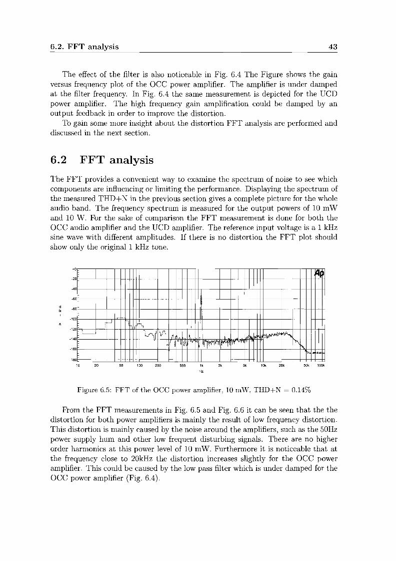
Figure 6.5: FFT of the aee power amplifier, 10 mW, THD+N = 0.14%
From the FFT measurements in Fig. 6.5 and Fig. 6.6 it can be seen that the thedistortion for both power amplifiers is mainly the result of low frequency distortion.This distortion is mainly caused by the noise around the amplifiers, such as the 50Hzpower supply hum and other low frequent disturbing signals. There are no higherorder harmonics at this power level of 10 mW. Furthermore it is noticeable that atthe frequency close to 20kHz the distortion increases slightly for the acc poweramplifier. This could be caused by the low pass filter which is under damped for theacc power amplifier (Fig. 6.4).
44 Chapter 6. Results
+0
-20
-40
-60
d-80
B
-100
A r-'-120r~
-140
-160
'\ ,~!
1 \
-180C=±=±=±:±±±±:±±==±:=:±:±±:±±±±I===::::l=±:::±::I::±±±i:±===:±=±=I:::::±±::f::±:±:J10 20 50 100 200 500 1k 2k 5k 10k 20k 50k lOOk
Hz
Figure 6.6: FFT of the UCD power amplifier, 10 mW, THD+N = 0.19%
SDk 100k20k10k5k2k1k
Hz
5002001005020
~ )0
0
0
0
o '-------, ~
: III llii,---1-l I
.. 1"\ J\0 u ~.f"'''L. i~ rw ~ l~rl\\ if~~~M W/M1¥ ,Vi'W0
0-1610
-2
-4
-6dB
-8
A-10
-12
-14
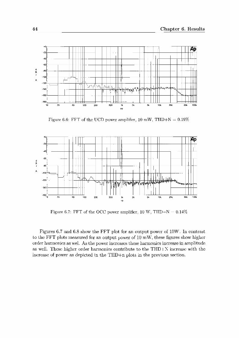
Figure 6.7: FFT of the acc power amplifier, 10 W, THD+N = 0.14%
Figures 6.7 and 6.8 show the FFT plot for an output power of lOW. In contrastto the FFT plots measured for an output power of 10 mW, these figures show higherorder harmonics as weI. As the power increases these harmonics increase in amplitudeas well. These higher order harmonics contribute to the THD+N increase with theincrease of power as depicted in the THD+n plots in the previous section.
6.3. THD+N Icepower 45
50k 100k20k10k5k2klk
Hz
5002001005020
~
0
0
h0
I---',
if.---! ; ILl.
0,re r~ I
!\(~
1ft ~i~r, ~ TVf'~i',
L~,ij 'I 1 If
0
0
-4
-6
-80
+0
-20
-14
-1610
-10
-12
A
dB
Figure 6.8: FFT of the UCD power amplifier, 10 W, THD+N = 0.21%
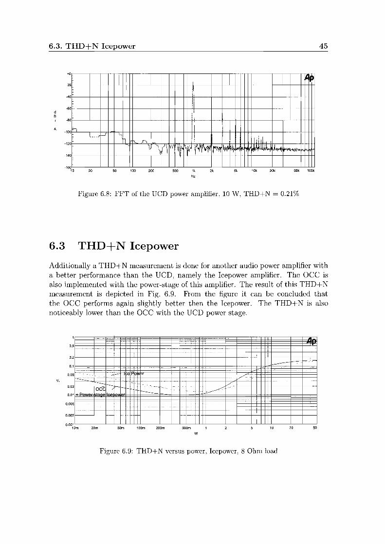
6.3 THD+N Icepower
Additionally a THD+N measurement is done for another audio power amplifier witha better performance than the UeD, namely the Icepower amplifier. The aee isalso implemented with the power-stage of this amplifier. The result of this THD+Nmeasurement is depicted in Fig. 6.9. From the figure it can be concluded thatthe aee performs again slightly better then the Icepower. The THD+N is alsonoticeably lower than the aee with the UeD power stage.
502010500m100m 200m50m20m
-----------
------ /'acc - . -'"
. :=-.~n. r---
10.0010m
0.002
0.005
0.01
0.02
0.5
0.05
0.1
0.2
%
w
Figure 6.9: THD+N versus power, Icepower, 8 Ohm load
46 Chapter 6. Results
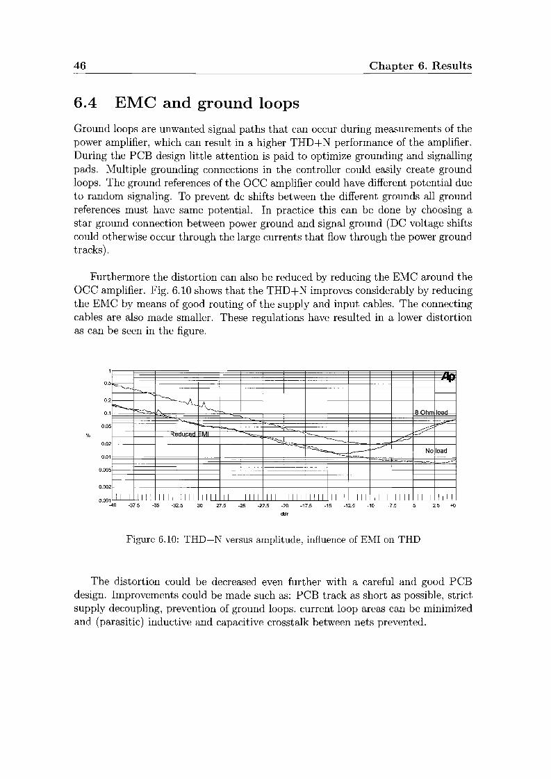
6.4 EMC and ground loops
Ground loops are unwanted signal paths that can occur during mea..'mrements of thepower amplifier, which can result in a higher THD+N performance of the amplifier.During the PCB design little attention is paid to optimize grounding and signallingpads. Multiple grounding connections in the controller could easily create groundloops. The ground references of the acc amplifier could have different potential dueto random signaling. To prevent dc shifts between the different grounds all groundreferences must have same potential. In practice this can be done by choosing astar ground connection between power ground and signal ground (DC voltage shiftscould otherwise occur through the large currents that flow through the power groundtracks).
Furthermore the distortion can also be reduced by reducing the EMC around theacc amplifier. Fig. 6.10 shows that the THD+N improves considerably by reducingthe EMC by means of good routing of the supply and input cables. The connectingcables are also made smaller. These regulations have resulted in a lower distortionas can be seen in the figure.
1
5
--------r--.... 'I\--.~1 ~ IA- R ()I
5R, dur-"'d MI ~ '~ .-/
2 ~.~~-~ ~
---::~ - i-----" No load
1 -=:: .-5
2
1 IIII IIII II II IIII III I II II IIII III I I III IIII II II I III III I II II III I III I
o.
0.0
%
0.0
0.0
0.00
0.00
o.
0.00-40 -37.5 -35 -32.5 -30 -27.5 -25 -22.5 -20 -17.5 -15 -12.5 -10 -7.5 -5 -2.5 +0
dBr
0.2
Figure 6.10: THD+N versus amplitude, influence of EMI on THD
The distortion could be decreased even further with a careful and good PCBdesign. Improvements could be made such as: PCB track as short as possible, strictsupply decoupling, prevention of ground loops, current loop areas can be minimizedand (parasitic) inductive and capacitive crosstalk between nets prevented.
Chapter 7
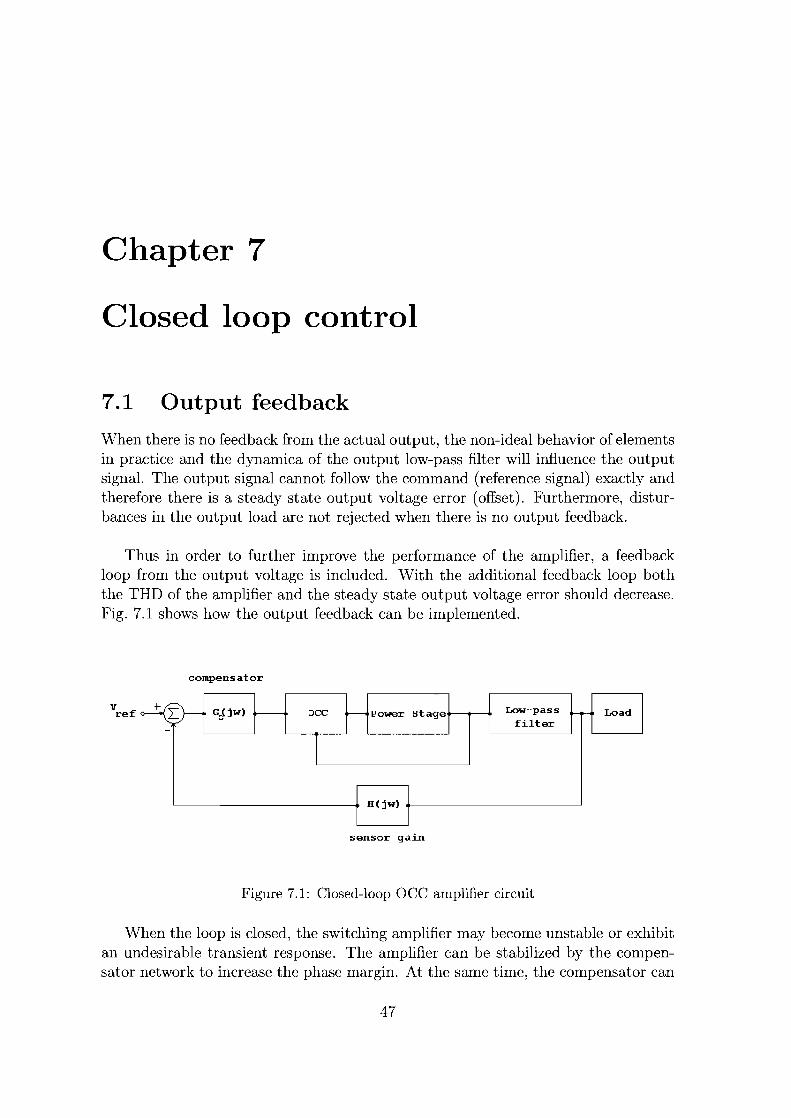
Closed loop control
7.1 Output feedback
When there is no feedback from the actual output, the non-ideal behavior of elementsin practice and the dynamica of the output low-pass filter will influence the outputsignal. The output signal cannot follow the command (reference signal) exactly andtherefore there is a steady state output voltage error (offset). Furthermore, disturbances in the output load are not rejected when there is no output feedback.
Thus in order to further improve the performance of the amplifier, a feedbackloop from the output voltage is included. With the additional feedback loop boththe THD of the amplifier and the steady state output voltage error should decrease.Fig. 7.1 shows how the output feedback can be implemented.
compensator
Vref~ Gjjw) 0--------, DCC 0-------, Power stage Low-pass ....,,...., Load
filter-
1
H(jw)
sensor gain
Figure 7.1: Closed-loop acc amplifier circuit
When the loop is closed, the switching amplifier may become unstable or exhibitan undesirable transient response. The amplifier can be stabilized by the compensator network to increase the phase margin. At the same time, the compensator can
47
48 Chapter 7. Closed loop control
also serve to shape the loop transfer function to achieve a desired transient response.In order to design the compensator the open loop transfer function of the acc poweramplifier is analyzed first.
7.2 Low-pass filter
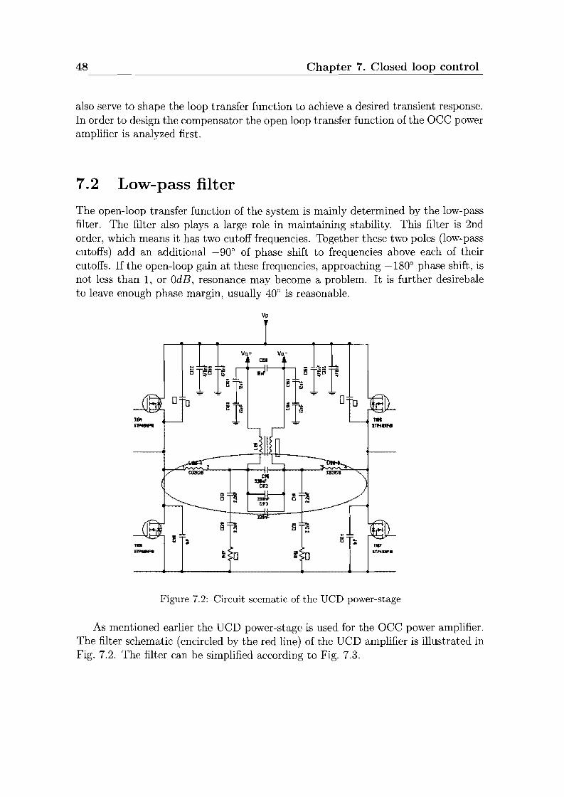
The open-loop transfer function of the system is mainly determined by the low-passfilter. The filter also plays a large role in maintaining stability. This filter is 2ndorder, which means it has two cutoff frequencies. Together these two poles (low-passcutoffs) add an additional -900 of phase shift to frequencies above each of theircutoffs. If the open-loop gain at these frequencies, approaching -180° phase shift, isnot less than 1, or OdE, resonance may become a problem. It is further desirebaleto leave enough phase margin, usually 400 is reasonable.
Vp
Figure 7.2: Circuit scematic of the UCD power-stage
As mentioned earlier the UCD power-stage is used for the acc power amplifier.The filter schematic (encircled by the red line) of the UCD amplifier is illustrated inFig. 7.2. The filter can be simplified according to Fig. 7.3.
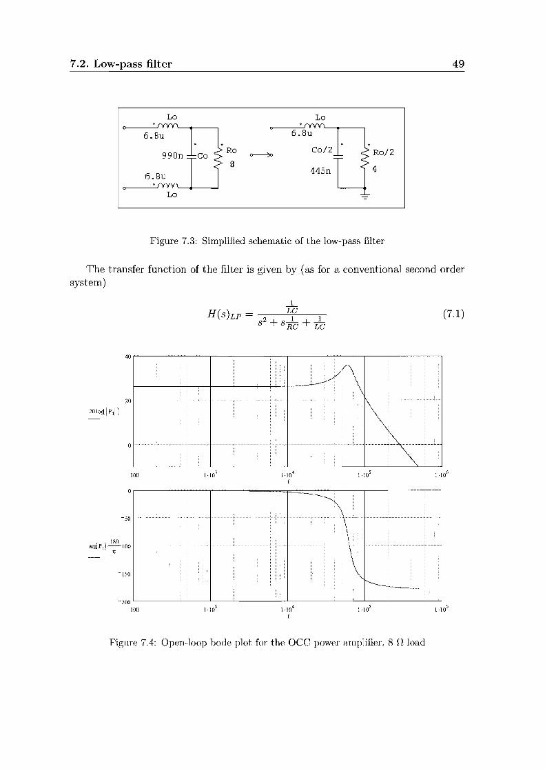
7.2. Low-pass filter 49
La La
Ra0--------70 Ra/2
8 46.8u
445n
0
La -=
Figure 7.3: Simplified schematic of the low-pass filter
The transfer function of the filter is given by (as for a conventional second ordersystem)
1
H(shp = 2 zP 1S + S RC + LC
(7.1)
40 ,...--------,.--------,.-----....,.--....,.-,.---....,.---....,.-,.---,
20 I·························· ' .. + .. , ... +
100
Or----....,.---r------~=r=::::::::::=--....,.--__r---__--___,
-50
ar~Pr)'~ lOa I························· , .." ···,·,·,··1·",···,···,·····",·""··"",, +:'j .. , ,.,.., +............ + +1,···",·";""""""",,'+"'11t
-200 '----- --'---__L--_--'--- L-- --'---_--'---L--_~ '___'_J
100
Figure 7.4: Open-loop bode plot for the oee power amplifier, 8 n load
50 Chapter 7. Closed loop control
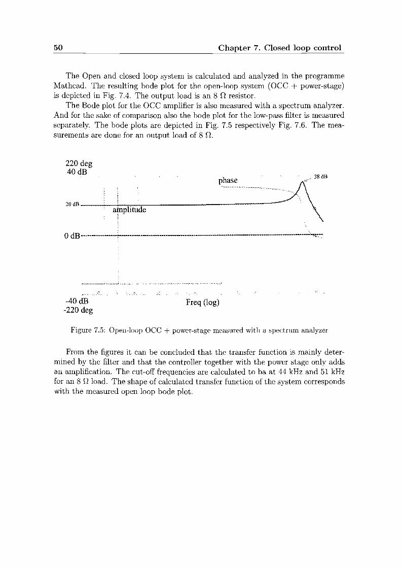
The Open and closed loop system is calculated and analyzed in the programmeMathcad. The resulting bode plot for the open-loop system (Oee + power-stage)is depicted in Fig. 7.4. The output load is an 8 n resistor.
The Bode plot for the oee amplifier is also measured with a spectrum analyzer.And for the sake of comparison also the bode plot for the low-pass filter is measuredseparately. The bode plots are depicted in Fig. 7.5 respectively Fig. 7.6. The measurements are done for an output load of 8 n.
220 deg40 dB
20 dB --.....L-
am
+-._P"="'li,...tu_d7""e---------P-~-m-se-..~~-..---..-~.--~~--------\~ ,,,a
:!
odB •.---...-------1'-----.--------.--..----.-....-.----...·--···--··-----·-------····---··-·---~::~~::7
-40 dB-220 deg
Freq (log)
Figure 7.5: Open-loop oee + power-stage measured with a spectrum analyzer
From the figures it can be concluded that the transfer function is mainly determined by the filter and that the controller together with the power stage only addsan amplification. The cut-off frequencies are calculated to ba at 44 kHz and 51 kHzfor an 8 n load. The shape of calculated transfer function of the system correspondswith the measured open loop bode plot.
7.3. Phase lead compensation 51
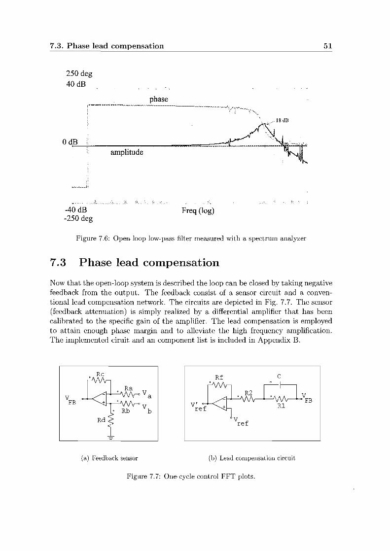
250 deg
40 dB
phase
amplitude
od~B----4 ==::::::::::.v.
-40 dB-250 deg
Freq (log)
Figure 7.6: Open-loop low-pass filter measured with a spectrum analyzer
7.3 Phase lead compensation
Now that the open-loop system is described the loop can be closed by taking negativefeedback from the output. The feedback consist of a sensor circuit and a conventionallead compensation network. The circuits are depicted in Fig. 7.7. The sensor(feedback attenuation) is simply realized by a differential amplifier that has beencalibrated to the specific gain of the amplifier. The lead compensation is employedto attain enough phase margin and to alleviate the high frequency amplification.The implemented ciruit and an component list is included in Appendix B.
VFB
Rc Rf c
Vf\!\~+--J\ \I\r-- FB
(a) Feedback sensor (b) Lead compensation circuit
Figure 7.7: One-cycle control FFT plots.

52 Chapter 7. Closed loop control
The transfer function of the phase lead network circuit is given by
(7.2)
where
K _ RfFB - RI +R2 T1 = RIC and
R2a=---
R 1 +R2
20 60
40
AD 10 arlbf f
20
0 0100 1 0 10
31 0 10
41 0 10
5 1 0 106 100 1 0 103 10104
1 0 105 1 0 106
f f
Figure 7.8: lied THD verus power, 4 n load
Figure 7.8 shows the corresponding frequency response of the implemented leadcompensator. When a is set to be 0.2 The compensator has one zero and one poleat f = 21r~lC = 26kHz respectively f = a21r~lC = I32kH z. The resistor values arechosen such that the flat band amplification is unchanged. RI = R2 = Rf/2 = Iknand C = 2nF
From Fig 7.9 one can see that the system is stable. This is justified by the phasemargin of about 30. In this amplifier, the output filter relies on a 8 n load for stability. If the gain of the amplifier was increased or load changed to different impedance,the system may become unstable and hence the compensator should be adapted.
7.3. Phase lead compensation
40 ,-------,--,---,--,-,--------...----...----..,---------,--,---,--,-----,
20 toi IP rl ) 20
20loi IHdrl)
a , , .
lOa
lOa r- --,--,--- ,....----,--,----,----- --,--,-,--- ...,........,
180arg{P r)·-
n
.J ) 180--100ar",Hd r .-
n
-200 '---~___'____'_____'____'.L..- -'----__.L..___-'----_ ____'____'_--'--'-J
lOa
Figure 7.9: Closed-loop OCC + power-stage
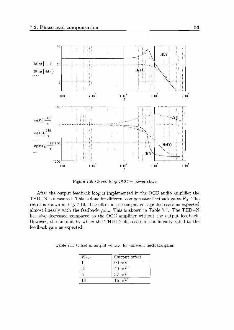
53
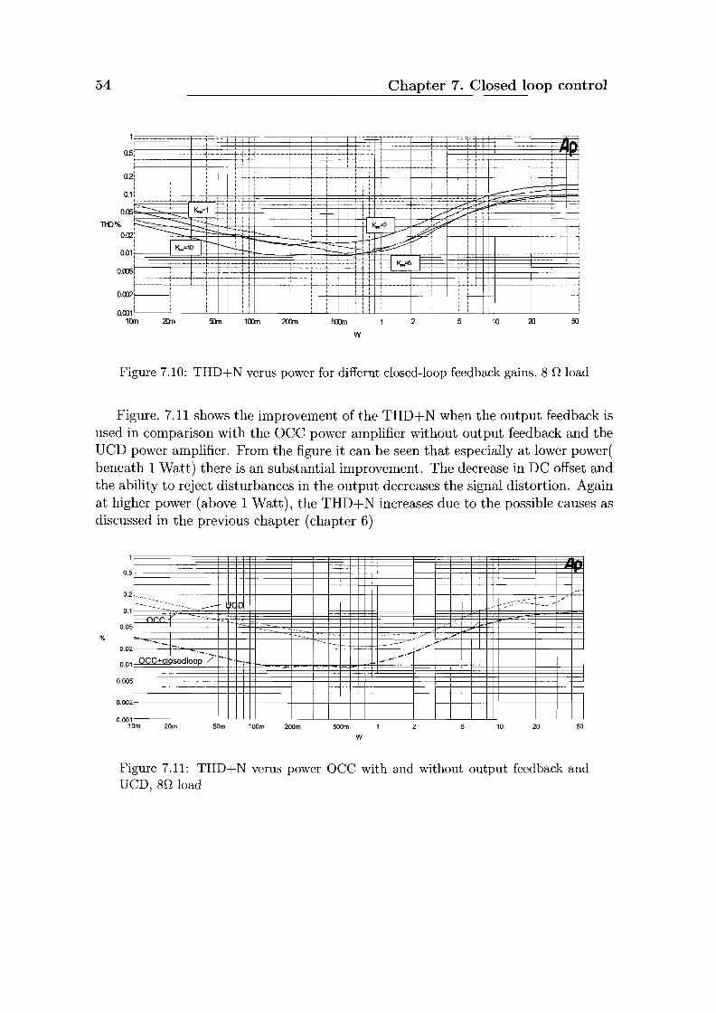
After the output feedback loop is implemented in the OCC audio amplifier theTHD+N is measured. This is done for different compensator feedback gains K d . Theresult is shown in Fig. 7.10. The offset in the output voltage decreases as expectedalmost linearly with the feedback gain. This is shown in Table 7.1. The THD+Nhas also decreased compared to the OCC amplifier without the output feedback.However, the amount by which the THD+N decreases is not linearly rated to thefeedback gain as expected.
Table 7.1: Offset in output voltage for different feedback gains
K FB Output offset1 90 mV2 49 mV5 37mV10 16 mV
54 Chapter 7. Closed loop control
n
, i
....... ------i................._--j
n
501052lOOno.cm LI__'--_--"-----'-...J....L.J...'--'-l__--'-----'-----'.-.L..LJ.--'-.LL_-.L_--'-..L..J--'-.LLLL_---.J_~...L_J
Kin
w
Figure 7.10: THD+N verus power for differnt closed-loop feedback gains, 8 0 load
Figure. 7.11 shows the improvement of the THD+N when the output feedback isused in comparison with the acc power amplifier without output feedback and theUCD power amplifier. From the figure it can be seen that especially at lower power(beneath 1 Watt) there is an substantial improvement. The decrease in DC offset andthe ability to reject disturbances in the output decreases the signal distortion. Againat higher power (above 1 Watt), the THD+N increases due to the possible causes asdiscussed in the previous chapter (chapter 6)
0.5~~ ~
%
0.02 '_
0.01 OCC+c1 sedl 00 v' _.-.-.-
0.005
0.002t----+--t--t-t-+-+-+t-+----i---+---+-+-1-+-f++--+--+--+-++-+-+++----+-+--+--t
50201052500m100m 200m20m0.001 '---_-'---_'---"------l-'-..L..L.LL.._---.l_--'--'----'---'-'---LLL__...J....----.L---l--'.....L.J..LL..L-_---'-_..L--'------l
10m
w
Figure 7.11: THD+N verus power acc with and without output feedback andUCD, 80 load
Chapter 8
Conclusions and recommendations
This report has presented a detailed analyse of the ane-cycle control method. Theoretical analysis have shown that the controller is able to control the duty-ratio inreal time such that in each switching cycle the average of the chopped waveform atthe switch output is exactly equal to the control reference. These analysis includesimulations of the aee used to control a buck converter and a full-bridge amplifier.A detailed analyses for component sensitivity is also presented for the controller.The double-edge modulation principle is also analyzed and implemented in the aeeto alleviate the switching frequency variation even more. Simulations of the aeemethod used to control a full-bridge power amplifier (class-D amplifier) have showngood results for power supply ripple rejection. The immediate rejection of the powersupply disturbance is the main characteristics of the aee.
Beside the theoretical analyses, practical measurements are performed to verifythe theoretical results. The aee is designed and implemented on a peB and usedto control a class-D power stage. The performance of the aee power amplifier isthen compared to the UeD power amplifier. As a result the experiments have shownthat aee power amplifier performs slightly better than the UeD amplifier. Theaee power amplifier could perform even beter if the power-stage is designed well.This is verified by the use of the Icepower power-stage.
Finally the aee power amplifier is extended with the addition of an outputfeedback. The output feedback is added to compensate for the disturbances in theoutput load and to reduce the offset in the output voltage. This has resulted in animproved THD+N performance of the aee power amplifier.
Although the improvement resulted from the addition of the output feedbackloop the performance could be improved even further especially for the higher outputpower. The power stage could be improved by decreasing the non-linearities in thestage. Furthermore, aee design could be improved also. The peB design canbe improved such that the influence of disturbance is minimized and ground loopsavoided.
55
Bibliography
[1] [SMI99] K. Mark Smith, Zheren Lai, and Keyue M. Smedley,A New PWM Controller with One-Cycle Responsein IEEE Trans. Power Electron. vol.14, no.1, pp. 142150, Jan 1999.
[2] [SME91] K. M. Smedley and S. Cuk,One cycle control of switching convertersIEEE PESC Conf. Rec., pp. 11731180, 1991
[3] [SME90] K. Smedley,Control Art of Switching ConvertersPh.D. Thesis, California Institute of Technology, 1990.
[4] [SME95] K. M. Smedley and S. Cuk,One cycle control of switching convertersIEEE Trans. Power Electron., vol, no.6, pp.625-633,Nov.1995.
[5] [LAI95] Z. Lai and K. M. Smedley,A new extension of one cycle control and its application to switching poweramplifiersIEEE Trans. Power Electron., vol. 11, pp. 99106, Nov. 1995.
[6] [AND96] N. Anderskouv, K. Nielsen, and M. Andersen,High fidelity pulse width modulation amplifiers based on novel double loop feedback techniques,in 100th Audio Engineering Society Convention, Copenhagen, Denmark,May1996
[7] [WEI04] W Wei, Z Jihong, X Dianguo, Z Guoliang ,A novel nonlinear control strategy for PWM DC-DC converter with optimizingtransient response ,Power Electronics and Motion Control Conference, 2004.
[8] [HOR94] P. Horowitz and W. Hill,The Art of Electronics. New York: Cambridge Univ. Press, 1994.
57
58 BIBLIOGRAPHY
[9] [WAN04] Y. Wang and S.Shen,Research on One-Cycle Control for Switching ConvertersProceedings of the 5th World Congress on Intelligent Control and automation,June 15-19, 2004
[10] [TSU04] Ma, D., Ki, W.-H., Tsui, C.-Y.,An integrated one-cycle control buck converter with adaptive output and dualloops for output error correctionIEEE Journal of Solid-State Circuits 39 (1), pp. 140-149, 2004
[11] [XU-03] Xu, F., Xu, D.-G., Liu, Y.-X. ,Novel nonlinear control method for PWM DC-DC converter with optimizingtransient responseZhongguo Dianji Gongcheng Xuebao/Proceedings ofthe Chinese Society of Electrical Engineering 23 (12), pp. 133-139, 2003
[12] [ZHA04] Hu, Z., Zhang, B., Deng, W. ,Feasibility study on one cycle control for PWM switched convertersPESC Record - IEEE Annual Power Electronics Specialists Conference 5, pp.3359-3365, 2004
[13] [LAI96] Z. Lai and K. M. Smedley,A general constant frequency pulse-width modulator and its applicationsin HFPC 96 Conf. Rec., pp. 279290
[14] [AUR05] Aurasopon, A., Kumhom, P., Chamnongthai, K.,emphOne-cycle control and random hysteresis in asynchronous sigma-delta modulationIEICE Transactions on Fundamentals of Electronics, Communications and Computer Sciences E88-A (2), pp. 469-475
[15] [JIN92] H. Jin, G. Joos, M. Pande, and F. Ziogas,Feedforward techniques using voltage integral duty-cycle control (for power convertors)PESC 92 Record. 23rd Annual IEEE Power Electronics Specialists Conference(Cat. No.92CH3163-3). Toledo, Spain, 29 June-3 July 1992. p. 370-7 vol.l.
[16] [LU-05] Lu, B., Brown, R., Soldano, M. ,Bridgeless PFC implementation using one cycle control techniqueConference Proceedings - IEEE Applied Power Electronics Conference and Exposition - APEC 2, art. no. 1453073, pp. 812-817
Appendix APcad Schematic
v v
111111111 'lIfT·r "1'1 mmnlIIITTTTI0 111TJ..1111 111 1.,-1..1 1 1 UlI-IIII-IILILLlU
~ 2Y , 7............. ;n1 1
1
~ i\Y{!l,.,··· .C:' c/'\n
."
h'~ ~:B
r-~;~ ~.,":" ..\ .... 'VV'v............ ~'-
1";
~;:
"'IL'l, ! "! U ···1···················· "
;: ~--'l
~1-/
~
__L~"oc.2I G~D,.'91
1 T
Figure A.I: Pcad schematic of the aee
60

Table A.I: List of components in the aee circuit
61
Component name valueResistor R2, R3 10 kn
Rl, R4 500 nR6, R7 4.7 knR8, R9, RlO 200 nRll, R12, R14, R15 10 knR13, R16 500 nR17, R18, R19, R20 1 kn
Capacitor Cl 2 nFC3, C4 4 nF
Logic And U18A U18B HEF4081BFLogic Inverter U3 HEF4000BFLogic Nor U8A U8C HEF400lBFLogic Xor U19A HEF4030BEYOperational Amplifier Ul, U2, U4, UI0, Ull AD8055Voltage regulator U9 L79M05
U17 L78M05Comparator U6A U6B, U7A LM319Analog multiplexer switch U13 74HC4052
62
I- ~~ '!.
Chapter A. Pcad Schematic
-.. :[!"" -.:<' :0
~~ eTi -:'
"-,
Figure A.2: Pcad PCB layout of the acc
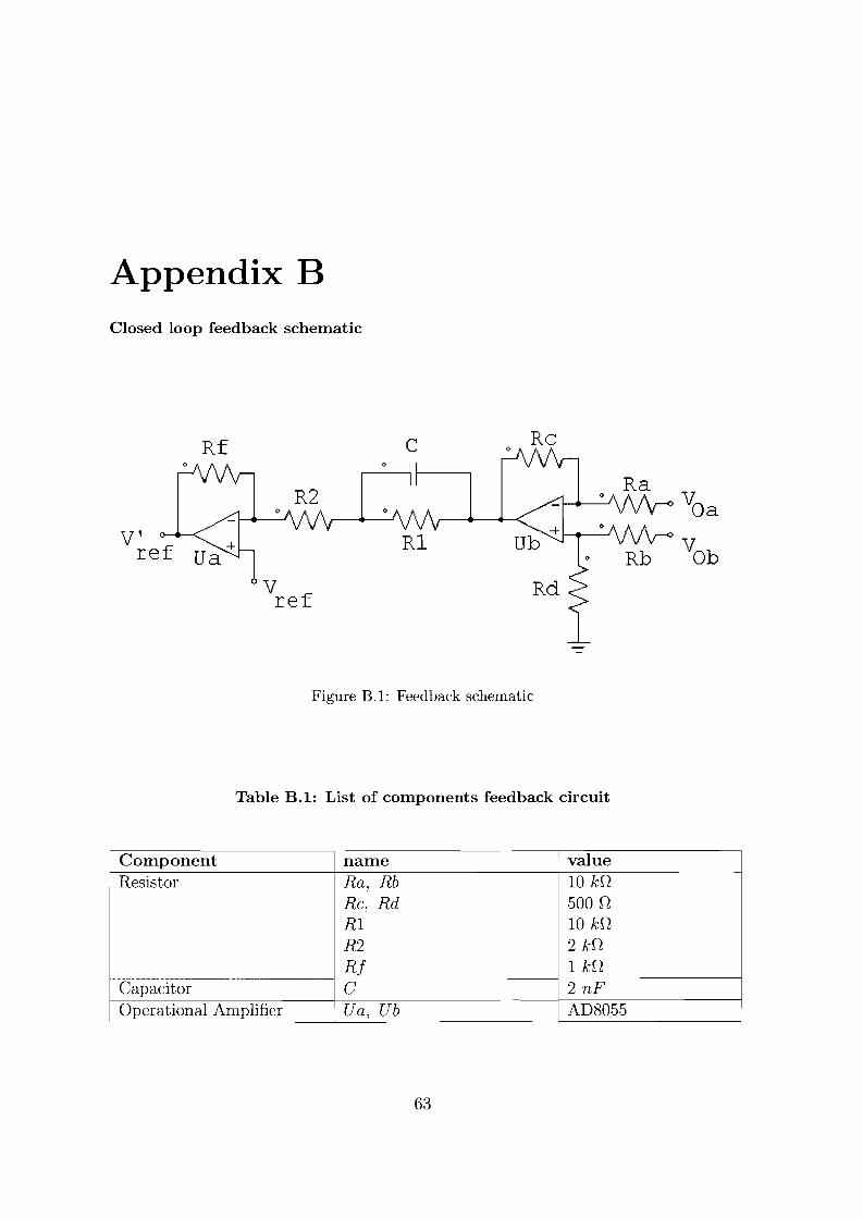
Appendix BClosed loop feedback schematic
Rf
R2
V'ref
o
c Rc
Figure B.l: Feedback schematic
Table B.l: List of components feedback circuit
Component name valueResistor Ra, Rb 10 kD
Rc, Rd 500 DR1 10 kDR2 2 kDRf 1 kD
Capacitor C 2 nFOperational Amplifier Ua, Ub AD8055
63

Appendix CMatlab code: calculation of the resetable integrator voltage
function Y=Howland(R,R1,R2,R3,C1,T);
%Y=Howland(R,R1,R2,R3,C1,Vin,T)
f=1000;w=2*pi*f;
% If R = (R1*R3)/R2, than the current into the capacitor depends only on% the input voltage and R, not on the capacitor voltage.
Vc=O;ta=O;tb=0.05e-7;t=0:0.05e-7:T;i=2;while i<length(t)+1
Yo)=O;Y(i) = 1/(C1)*QUAD(@fun,ta,tb, [J, [J ,R,R1,R2,R3,Vc,w);Vc=Vc+y(i) ;Z(i)=Vc;ta=tb;tb=tb+0.05e-7;i=i+1;
end
tz=0:0.05e-7:6e-7;plot(tz,-4,'b. ');holdplot(t,Z);axis([O 0.6e-6 -5 OJ) ,grid,ylabel('Resetable Integrator Voltage'); xlabel('Time');
64

%Total current into the capacitor
function Ic=fun(t,R,Rl,R2,R3,Vc,w);
Vin=70 + 5*sin(w*t);Ic = (-Vin+Vc)/R + R2*Vc/(Rl*R3);
65

Appendix DMatlab code: calculation of is variation due to supply ripple
%Leading edge function to solve switching time ta
function ta_L=taLeading(FO,phi,Vref)
for i=l:length(phi)ta_L(i)=fzero(@(t) Int_g(t,FO,phi(i),Vref),O);
end
function y=Int_g(ta_L,FO,phi,Vref)
%This is (l!TO)int_O-ta 2g(t)dty=quad(@g,O,ta_L, [], [] ,phi)*FO;y=-2*y+g(ta_L,phi)-Vref;
function y=g(t,phi)y=1+0.2*sin(2*pi*250*t+phi);
%Leading edge function to solve switching frequence Fs
function Ts_L=TsLeading(FO,phi,Vref)ta_L=taLeading(FO,phi,Vref);
for i=l:length(ta_L)Ts_L(i)=fzero(@(t) Int_eqn(t,ta_L(i) ,phi(i) ,Vref) ,0);
end
66

67
%This is int_O-ta (g(t)-Vref)dt + int_ta-Ts (-g(t)-Vref)dty=quad(@X,O,ta_L,[],[] ,phi,Vref)+ quad(@Z,ta_L,Ts_L,[],[] ,phi,Vref);
function y=X(t,phi,Vref)y= -(1+0.2*sin(2*pi*250*t+phi))-Vref;
function y=Z(t,phi,Vref)y= 1+0.2*sin(2*pi*250*t+phi)-Vref;
% double edge modulation , summerizing Ts_T for the trailing edge and Ts_L% for the leading edge
function Fs_Double_norm = double_edge(FO,phi,Vref)
Ts_T=TsTrailing(FO,phi,Vref);Ts_L=TsLeading(FO,phi,Vref);
for i=l:length(Ts_T)Fs_Double(i) = l/(Ts_T(i)+Ts_L(i));
Fs_Double_norm(i) = Fs_Double(i)/(O.5*FO);end
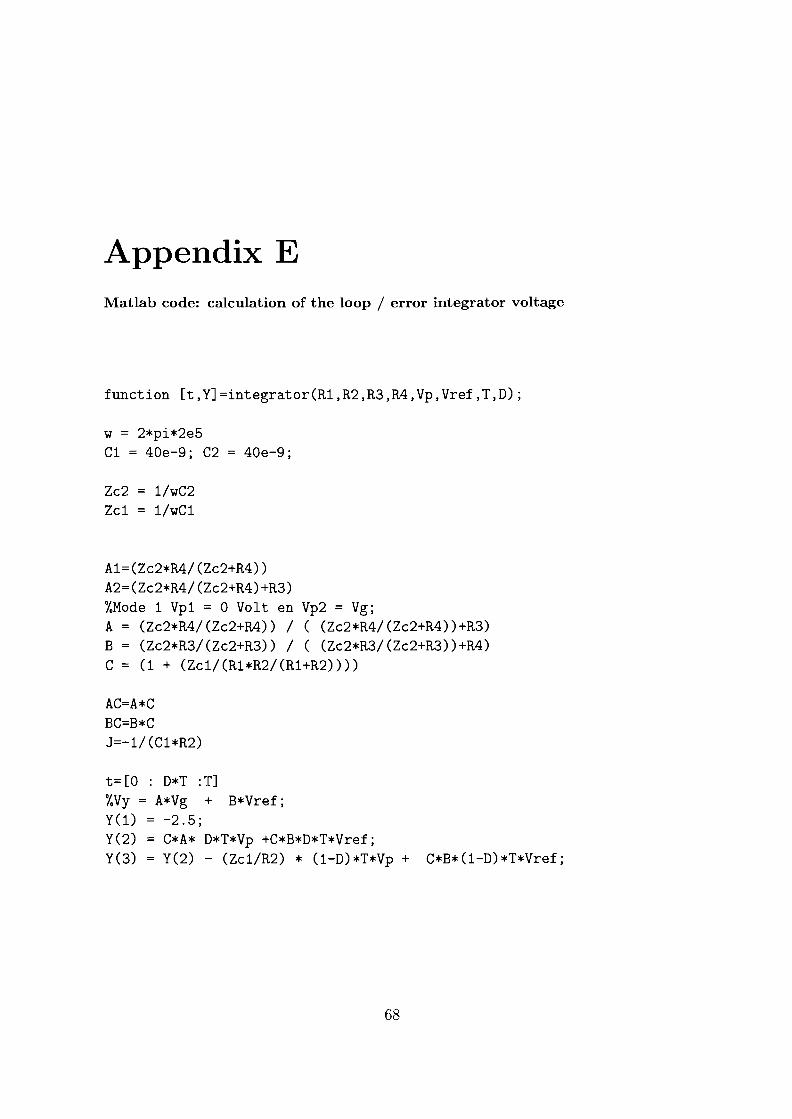
Appendix EMatlab code: calculation of the loop / error integrator voltage
function [t,Y]=integrator(R1,R2,R3,R4,Vp,Vref,T,D);
w = 2*pi*2e5C1 = 40e-9; C2 = 40e-9;
Zc2 1/wC2Zc1 1/wC1
A1=(Zc2*R4/(Zc2+R4))A2=(Zc2*R4/(Zc2+R4)+R3)%Mode 1 Vp1 = 0 Volt en Vp2 = Vg;A = (Zc2*R4/(Zc2+R4)) / ( (Zc2*R4/(Zc2+R4))+R3)B = (Zc2*R3/(Zc2+R3)) / ( (Zc2*R3/(Zc2+R3))+R4)C = (1 + (Zc1/(R1*R2/(R1+R2))))
AC=A*CBC=B*CJ=-1/(C1*R2)
t= [0 : D*T :T]%Vy = A*Vg + B*Vref;YO) = -2.5;Y(2) = C*A* D*T*Vp +C*B*D*T*Vref;Y(3) = Y(2) - (Zc1/R2) * (1-D)*T*Vp + C*B*(1-D)*T*Vref;
68