Embed Size (px)
Citation preview
Eindhoven University of Technology
MASTER
Plasma and in situ film studies on silicon nitride growth for photovoltaic applications
van Assche, F.J.H.
Award date:2006
Link to publication
DisclaimerThis document contains a student thesis (bachelor's or master's), as authored by a student at Eindhoven University of Technology. Studenttheses are made available in the TU/e repository upon obtaining the required degree. The grade received is not published on the documentas presented in the repository. The required complexity or quality of research of student theses may vary by program, and the requiredminimum study period may vary in duration.
General rightsCopyright and moral rights for the publications made accessible in the public portal are retained by the authors and/or other copyright ownersand it is a condition of accessing publications that users recognise and abide by the legal requirements associated with these rights.
• Users may download and print one copy of any publication from the public portal for the purpose of private study or research. • You may not further distribute the material or use it for any profit-making activity or commercial gain
Eindhoven University of Technology Department of Applied Physics Equilibrium and Transport in Plasmas (ETP)
Advisors:
Dr.ir. W.M.M. Kessels Dr. J.Hong
Plasma and in situ film studies on silicon nitride growth for
photovoltaic applications
F.J.H. van Assche
April 2002, ETP 02-06
Prof.dr.ir. M.C.M. van den Sanden
Abstract
Amorphous hydrogenated silicon nitride (a-SiNx:H) has an important application as antireflection coating, and surface and bulk passivating layer on crystalline silicon solar cells. In this study, the feasibility of the expanding thermal plasma technique for the deposition of a-SiNx:H at high rates (typically 20 nm/s) has been investigated. By implementation of high rate deposited a-SiNx:H films in multicrystalline silicon solar cells, proruising antireflection and bulk passivating qualities have been demonstrated.
In order to assist future optirnization of the process, the growth mechanism of a-SiNx:H using a SiH4-
N2 type of plasma has been studied. As a starting point for this study, a previously proposed growth model (Srnith et al., J. Vac. Sci. Technol. B 8, 551 (1990)) has been used. In this model, the a-SiNx:H growth is portrayed by surface reactions of activated nitrogen with an a-Si:H-like top layer.
The plasma densities of viabie candidate species for respectively the a-Si:H growth and 'nitridation' reactions have been investigated. Using threshold ionization mass spectroscopy (TIMS), the atomie N densi_t~ has been mea~ured in bo~h the non-11epo2~itin_~ 'souree plasma' wit_hout SiH4, and during deposit~on cond1tlons. A very h1gh N dens1ty of -10 -10 m · has been revealed m the souree plasma and durmg 'standard' deposition conditions. Using cavity ringdown spectroscopy (CRDS), SiH3 densities of -1018
-
1019 m·3 have been observed during deposition, and SiH densities of -1016-10 17 m·3• At these densities,
SiH3 can almost fully account for the Si growth flux, while SiH has a contribution in the order of percentages. The high N radical density in the plasma could certainly account for the N growth flux. If the N radicals indeed are responsible for the growth, the sticking probability of N is estimated to be in the order of a few percent.
Furthermore, a new infrared absorption measurement technique, attenuated total reflection Fourier transfarm infrared spectroscopy (ATR-FTIR), has been installed for in situ studies on as-deposited aSiNx:H films. With this technique, the infrared absorptions by Si-N, Si-H and N-H honds have been monitored as a function of the film thickness. From the revealed depth information, a relatively homogeneaus bonding configuration is observed as a function of the film depth, compared to a-Si:H growth.
In addition, the A TR-FTIR technique has been used to find more evidence for the growth model of Smith. If this model is applicable, it should be possible to create a-SiNx:H at the surface of an a-Si:H film, by modifying the a-Si:H film with a N-containing plasma. This has indeed been confirmed in a 'nitridation' experiment, in which an as-deposited a-Si:H film has been exposed to an Ar/N2 plasma. The measured changes in the infrared absorption spectrum suggest that the plasma treatment results in the creation of an a-SiNx:H surface layer with a depth of -2 nm. This has been found to occur without strong dependenee on the substrate temperature in the range of 1 00-400°C, which is in line with the only weakly temperature dependent N/Si content of the films during normal deposition conditions.
As a conclusion, both the plasma studies and the nitridation experiment corroborate the proposed aSiNx:H growth model of Smith et al .. As an extension to this model, the measured radical densities in the plasma indicate that the formation of the a-Si:H-like layer can almost fully be accounted for by SiH3
radicals, while the role of the activated nitrogen could well be filled in by the N radical.
Table of contents
ABSTRACT •................................................................................................................................................................ 11
1. INTRODUCTION .................................................................................................................................................... 1
1.1 Technology assessment ............................................................................................................................... 1 1.2 ETP-deposited a-SiN,:H as antireflection and bulk passivating material on me-Si solar cells ................... 3
1.2.1 Cascaded are generated expanding thermal plasma: general characteristics ................................... .3 1.2.2 ETP-deposited a-SiNx:Hfor me-Si solar cells .................................................................................... .4
1.3 A-SiN,:H deposition mechanisms ............................................................................................................... 7 1.4 Goal of this investigation and outline of the report.. ................................................................................... 8
2. PLASMAAND SURFACE MEASUREMENT TECHNIQUES .......................................................................... 9
2.1 Cavity ring down spectroscopy (CRDS): SiH and SiH3 radical density ..................................................... 9 2. 1.1 The basicsof CRDS ............................................................................................................................. 9 2.2.2 CRDS on SiH3 .........•.......................................................................................................................... 10 2.2.3 CRDS on SiH ..................................................................................................................................... 12
2.2 Threshold ionization mass speetrometry ................................................................................................... 17 2.2.1 Quadrupale mass speetrometry ......................................................................................................... 17 2.2.2 Beam and background density ........................................................................................................... 18 2.2.3 Radical density measurement: threshold ionization mass spectrometry ............................................ 18 2.2.4 Converting detection rates to densities .............................................................................................. 20 2.2.5 Further experimental detailsjortheN radical measurements .......................................................... 21
2.3 Attenuated total reflection infrared spectroscopy ...................................................................................... 23 2.3.1 The principle of ATR spectroscopy: the evanescent wave ................................................................. 23 2.3.2 Converring absorbances to densities ................................................................................................. 25 2.3.3 The experimental setup ...................................................................................................................... 28 2.3.4 Comparison between Si and ZnSe ATR crystal materials ................................................................. .31
3. PLASMA RADICAL DENSITIES DURING A-SINx:H DEPOSITION .......................................................... 33
3.1 Precursor dissociation mechanisms ........................................................................................................... 33 3.2 N and H radical densities from the Ar/N2/H2 plasma source ..................................................................... 34 3.3 N, SiH3 and SiH radical densities in the Ar/H2/N2/SiH4 depositing plasma .............................................. 34 3.4 Contribution of SiH3, SiH and N radicals to the film growth .................................................................... 36
4. IN SITU FILM STUDY .......................................................................................................................................... 41
4.1 N-rich- Si-rich a-SiN,:H films ................................................................................................................ .41 4.2 Depth information .................................................................................................................................... .45 4.3 Ni tridation of an a-Si:H film .................................................................................................................... .46
4.3.1 Ar plasnla treatment of a-Si:H ........................................................................................................... 46 4.3.2 Ar/N2 plasma treatment: nitridation of a-Si:H. .................................................................................. 47 4.3.3 Nitridation vs temperature ................................................................................................................. 49
5. CONCLUSIONS ..................................................................................................................................................... 51
DANKWOORD .......................................................................................................................................................... 53
REFERENCES ........................................................................................................................................................... 55
APPENDIX: ABSORPTION VS. ABSORBANCE ................................................................................................. 57
Chapter 1: Introduetion
Chapter 1
Introduetion
1.1 Technology assessment An important strategy for achieving a reduction of the global C02 ernission, is making clean energy
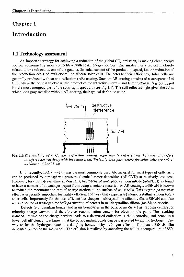
sourees economically more competitive with fossil energy sources. This master thesis project is closely related to this subject, as one of the goals is the enhancement of the production speed, i.e. the reduction of the production costs of multicrystalline silicon solar cells. To increase their efficiency, solar cells are generally produced with an anti reflection (AR) coating. Such an AR coating consists of a transparent IJ4 film, where the optica! thickness (the product of the refractive index n and film thickness d) is optirnized for the most energetic part of the solar light spectrum (see Fig.l.l). The still reflected light gives the cells, which look gray metallic without AR-coating, their typical dark blue color.
A~625nm destructive interference
/
nd=A/4
Fig.l.l:The working of a À/4 anti reflection coating: light that is reflected on the internat surface interferes destructively with incoming light. Typically used parameters for solar cells are nz2.1, d::70nm and ?.:=625 nm.
Until recently, TiOx (n=-2.0) was the most commonly used AR material for most types of cells, as it can be produced by atmospheric pressure chemica! vapor deposition (AP-CVD) at relatively low cost. However, for (multi-)crystalline silicon cells, hydrogenated amorphous silicon nitride (a-SiNx:H), is found to have a number of advantages. Apart from being a suitable material for AR coatings, a-SiNx:H is known to reduce the recombination rate of charge carriers at the surface of solar cells. This surface passivation effect is especially important for highly efficient and very thin (expensive) monocrystalline silicon (c-Si) solar cells. Importantly for the less efficient but cheaper multicrystalline silicon cells, a-SiNx:H can also act as a souree of hydrogen for bulk passivation of defects in multicrystalline silicon (me-Si) solar cells.
Defects (e.g. dangling honds) and grain boundaries in the bulk of me-Si act as trapping centers for minority charge carriers and therefore as recombination centers for electron-hole pairs. The resulting reduced lifetime of the charge carriers leads to a decreased collection at the electrodes, and hence to a lower cell efficiency. It is known that the bulk dangling honds can be passivated by atomie hydrogen. One way to let the hydragen reach the dangling honds, is by hydrogen effusion from an a-SiNx:H film deposited on top of the me-Si cell. The effusion is realized by annealing the cell at a temperature of 850-
Plasma and in situ film studies on silicon nitride growth for photovoltaic applications
900oc*. After the annealing process, cell efficiencies are seen to increase, due to an increased internal quanturn efficiency (IQE) for long (red) wavelengths. This indeed indicates a bulk effect, as long wavelength light is able to penetrate deep into the cell.
However, although a-SiN,:H films clearly increase solar cell efficiencies, their implementation in the cells has to compete with the relatively cheap production process ofTiO, AR coatings. A-SiN,:H films are traditionally deposited by plasma deposition radio frequent (RF) wave generated plasmas, and more recently also with microwave (MW) plasma's (ECN), at low pressures ( -10-5 mbar). With these techniques only low growth rates (0.01-lnm/s) can be achieved, which makes the implementation of aSiN,:H films in solar cells relatively expensive. Therefore in the plasma-group, a-SiN,:H deposition with a cascaded are generated expanding thermal plasma (ETP) has been investigated. With this plasma, aSiN,:H deposition rates of -20nm/s are in principle possible.
In this master thesis project, two issues have been addressed. The feasibility of ETP-films as AR coating and as bulk passivation layer has been investigated by implementation of the films in a series of n + p me-Si solar cells. Th is was done in cooperation with Energieonderzoek Centrum Nederland (ECN) and Shell Solar Helmond. The solar cells produced with ETP a-SiN,:H have shown proruising results, which indicate that the ETP technique is viabie for industrial production of a-SiN,:H coatings for solar cells.
While the ETP process will be improved by further fine-tuning of the plasma parameters, also fundamental insight in the deposition mechanism can be of value to control and imprave the process in the future. Therefore, also efforts have been made to gain more understanding of the plasma and surface processes that lead to a-SiN,:H deposition. It has been investigated which reactive species are present in the plasma, that could be responsible for the deposition. As a starting-point, publisbed information on conventional a-SiN,:H depositing plasmas is used, as well as knowledge of ETP deposition of hydrogenated amorphous silicon (a-Si:H) in the group. The combination of both has enabled aimed investigation of candidate reactive depositing species in the plasma.
Strongly related to the deposition mechanism are the basics of the bulk passivation process. The amount of bulk passivation depends on various film properties, among which the hydrogen bonding configuration (i.e. bonded to Si or N) and the film density. Furthermore, the transparency of the films is related to their optica! bandgap, which depends on the general bonding configuration as well. For these reasons, the H-bonding configuration in the deposited films has been investigated with a sensitive in-situ infra red absorption measurement technique.
In the following section, a brief description will be given of the cascaded are expanding thermal plasma, with attention to the relevant properties for a-SiN,:H deposition. As an illustration, the feasibility of the ETP films as AR and bulk passivation layer is then demonstrated by showing the test results of a solar cell in section 1.2.2. In section 1.3, a treatment of some of the present knowledge of the a-SiN,:H deposition process is given, followed by a more precise target formulation of the second part of this research. Finally, the contentsof this report are given.
• In solar cell production, the hydrogen effusion is generally combined with the metallization step (application of electrodes), in a so-called 'firing through' process. In this process, silver from a screen-printed silver-paste metallization pattem on top of the cell, diffuses through the a-SiNx:H AR coating to the me-Si.
2
Chapter 1: Introduetion
1.2 ETP-deposited a-SiNx:H as antireflection and bulk passivating material for multicrystalline silicon photovoltaic cells
An important characteristic of the expanding thermal plasma (ETP), from an industrial point of view, is its ability to rnaintaio a high dissociation rate at high gas flows. Th is enables very high deposition ( or etching) rates for several materials. For example, a-Si:H deposition rates of 10 nm/s and a-SiN:H deposition rates of over 20 nm/s have been achieved, where conventional MW and RF plasmas reach only deposition rates of maximum 1 nm/s. Furthermore, due to absence of a bias-voltage, the substrate is free from ion-bombardment during deposition.
A useful property of the ETP for scientific studies, in which well-defined and reproducible experiments are of value, is the fact that it is a remote plasma: the plasma souree and the substrate chamber are geometrically separated. A large pressure difference between the plasma souree and the downstream chamber enables tuning of the plasma parameters to a large degree independently from the substrate properties •. Furthermore, the plasma souree itself can be kept free from undesired deposition, by injection of the deposition precursor gas in the expansion chamber.
In the next section, a description is given of the ETP plasma technique.
1.2.1 Cascaded are generated expanding thermal plasma: general characteristics
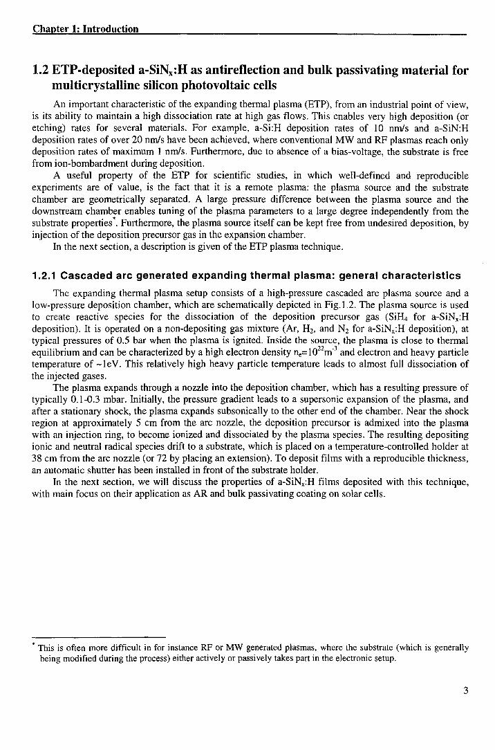
The expanding thermal plasma setup consists of a high-pressure cascaded are plasma souree and a low-pressure deposition chamber, which are schematically depicted in Fig.l.2. The plasma souree is used to create reactive species for the dissociation of the deposition precursor gas (SiH4 for a-SiNx:H deposition). lt is operated on a non-depositing gas mixture (Ar, H2, and N2 for a-SiNx:H deposition), at typical pressures of 0.5 bar when the plasma is ignited. Inside the source, the plasma is close to thermal equilibrium and can be characterized by a high electron density ne=l022m-3 and electron and heavy partiele temperature of -1 eV. Th is relatively high heavy partiele temperature leads to al most full dissociation of the injected gases.
The plasma expands through a nozzle into the deposition chamber, which has a resulting pressure of typically 0.1-0.3 mbar. Initially, the pressure gradient leads to a supersonic expansion of the plasma, and after a stationary shock, the plasma expands subsonically to the other end of the chamber. Near the shock region at approximately 5 cm from the are nozzle, the deposition precursor is admixed into the plasma with an injection ring, to become ionized and dissociated by the plasma species. The resulting depositing ionic and neutral radical species drift to a substrate, which is placed on a temperature-controlled holder at 38 cm from the are nozzle (or 72 by placing an extension). To deposit films with a reproducible thickness, an automatic shutter has been installed in front of the substrate holder.
In the next section, we will discuss the properties of a-SiNx:H films deposited with this technique, with main focus on their application as AR and bulk passivating coating on solar cells.
* This is aften more difficult in for instanee RF or MW generated plasmas, where the substrate (which is generally being modified during the process) either actively or passively takes part in the electronic setup.
3
Plasma and in situ film studies on silicon nitride growth for photovoltaic applications
Ar+ N2 + H2
~ Cathode (3x)
cascaded
I
shutter to roots+
11.1 rbo PLUTIP
back flow
Fig.1.2: The cascaded are thermal plasma souree (left), and the complete expanding thermal plasma setup (right). The cascaded are plasma souree consists of a stack of electrically insulated capper plates, with concentric holes (04mm) for inlet of gases. The plasma is generated by means of a current controlled are discharge between three tungsten cathode tips at one side of the plates and the anode at the other side. Typical cu1-rents are 10-75A, and the power dissipated is 2-5 kW. Typical used gas flows are 55 sccs (standard cubic centimeters per second) Ar, 0-10 sccs H2 and 0-12 sccs N2, with downstream il1jection of 1-10 sccs SiH4• The resulting mixture of ionic and neutral radical species expands towards the substrate holder, which is temperafure controlled (0-500°C). A helium back flow is used to increase thermal contact between the holder and substrate. The reactor windows allow for several process diagnostics of which some are discussed in this report.
1.2.2 ETP-deposited a-SiNx:H for me-Si solar cells
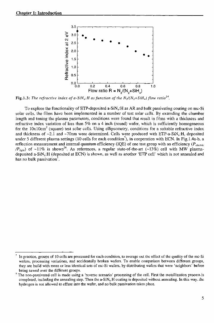
A-SiNx:H can be deposited with the ETP deposition technique, using an Ar/Hz/Nz gas mixture in the cascaded are, and Si~ as precursor in the expansion chamber'. As shown in Fig.1.3, the refractive index is tunable by varying the N2/SiH4 gas flow ratio24
• The resulting films have a refractive index that ranges from 1.7 (N-rich) to 3.25 (noN). This is useful for AR applications.
* An important alternative gas mixture for a-SiNx:H deposition is the combination of Ar/H2 in the are, with SiH4 and NH3 as precursor gases in the chamber. In this report, we will concentrate on the N2 mixture.
4
Chapter 1: Introduetion
3.5
> 3.0 Q) • C\1 • - 2.5 ctl x
• • • • • Q) 2.0 • '0 c • • Q) 1.5 > :;:::;
1.0 0 ctl ..... - 0.5 Q)
a: 0.0
0.0 0.2 0.4 0.6 0.8 1.0 Flow ratio R = N/(N
2+SiH
4)
Fig.1.3: The refractive index of a-SiNx:H as function of the Nzi(N2+SiH4 ) flow ratio 24.
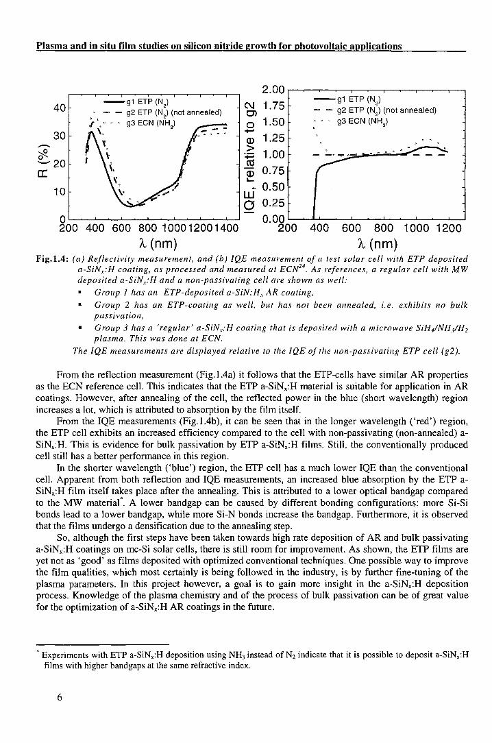
To explore the functionality of ETP-deposited a-SiNx:H as AR and bulk passivating coating on me-Si solar cells, the films have been implemented in a number of test solar cells. By extending the chamber length and tuning the plasma parameters, conditions were found that result in films with a thickness and refractive index variation of less than 5% on a 4 inch (round) wafer, which is sufficiently homogeneaus for the lüx 10cm2 (square) test solar cells. Using ellipsometry, conditions for a suitable refractive index and thickness of -2.1 and -70nm were determined. Cells were produced with ETP-a-SiNx:H, deposited under 5 different plasma settings (1 0 cells for each condition *), in cooperation with ECN. In Fig.l.4a-b, a reflection measurement and internat quanturn efficiency (IQE) of one test group with an efficiency (P etectric
1Pug111) of -11% is shown24. As references, a regular state-of-the-art ( -13%) cell with MW plasma
deposited a-SiNx:H (deposited at ECN) is shown, as wellas another 'ETP cell' which is not annealed and has no bulk passivation t.
In practice, groups of 10 cells are processed for each condition, to average out the effect of the quality of the me-Si wafers, processing variations, and accidentally broken wafers. To enable comparison between different grou{ls, they are build with more or less identical sets of me-Si wafers, by distributing wafers that were 'neighbors' before being sa wed over the different groups.
t The non-passivated cell is made using a 'reverse scenario' processing of the cell. First the metallization prooes:<1. is completed, including the annealing step. Then the a-SiNx:H coating is deposited without annealing. In this Wa}', lhe hydrogen is notallowed to effuse into the wafer, and no bulk passivation takes place.
5
Plasma and in situ film studies on silicon nitride growth for photovoltaic applications
40 -g1 ETP (N
2)
- - g2 ETP (N2
) (not annealed) :r '. · o • g3 ECN (NH)
30 \,
~ -'"::!!. .
0 --20 a:
10
0 200 400 600 800 1 000 1200 1400
À (nm)
C\1 0> 0 +-'
Q)
> +-' co Q) ~
w a
2.00
1.75
1.50
1.25
1.00
0.75
0.50
0.25
0.00 200
--g1 ETP (N) - g2 ETP (N) (not annealed) · g3 ECN (NH
3)
400 600 800 1000 1200
À (nm) Fig.1.4: (a) Reflectivity measurement, and (b) IQE measurement of a test solar cell with ETP deposited
a-SiNx:H coating, as processed and measured at ECN24. As references, a regular cell with MW
deposited a-SiNx:H and a non-passivaring cel! are shown as wel!:
• Group 1 has an ETP-deposited a-SiN:Hx AR coating,
• Group 2 has an ETP-coating as wel!, but has not been annealed, i.e. exhibits no bulk passivation,
• Group 3 has a 'regular' a-SiNx:H coating that is deposited with a microwave SiH4/NH3/H2
plasma. This was done at ECN.
The IQE measurements are displayed relative to the JQE of the non-passivaring ETP cel! ( g2 ).
From the reflection measurement (Fig.l.4a) it follows that the ETP-cells have similar AR properties as the ECN reference cell. This indicates that the ETP a-SiNx:H material is suitable for application in AR coatings. However, after annealing of the cel!, the reflected power in the blue (short wavelength) region increases a lot, which is attributed to absorption by the film itself.
From the IQE measurements (Fig.l.4b), it can beseen that in the Jonger wavelength ('red') region, the ETP cell exhibits an increased efficiency compared to the cell with non-passivating (non-annealed) aSiNx:H. This is evidence for bulk passivation by ETP a-SiNx:H films. Still, the conventionally produced cell still has a better performance in this region.
In the shorter wavelength ('blue') region, the ETP cell has a much lower IQE than the conventional cell. Apparent from both reflection and IQE measurements, an increased blue absorption by the ETP aSiNx:H film itself takes place after the annealing. This is attributed to a lower optica! bandgap compared to the MW materia( A lower bandgap can be caused by different bonding configurations: more Si-Si honds lead to a lower bandgap, while more Si-N honds increase the bandgap. Furthermore, it is observed that the films undergo a densification due to the annealing step.
So, although the first steps have been taken towards high rate deposition of AR and bulk passivating a-SiNx:H coatings on me-Si solar cells, there is still room for improvement. As shown, the ETP films are yet not as 'good' as films deposited with optimized conventional techniques. One possible way to improve the film qualities, which most certainly is being foliowed in the industry, is by further fine-tuning of the plasma parameters. In this project however, a goal is to gain more insight in the a-SiNx:H deposition process. Knowledge of the plasma chernistry and of the processof bulk passivation can be of great value for the optimization of a-SiNx:H AR coatings in the future.
* Experiments with ETP a-SiNx:H deposition using NH3 instead of N2 indicate that it is possible to deposit a-SiN.:H films with higher bandgaps at the same refractive index.
6
Chapter 1: Introduetion
As a starting point for the investigation described in the following chapters, we will discuss some of the existing publisbed work on a-SiNx:H deposition mechanisms in the next section. As the expanding thermal plasma is not very common yet, most workis based upon MW and RF generated plasmas.
1.3 A-SiNx:H deposition mechanisms A remarkable condusion in ref.l and 2, is that the plasma chemistry is relatively simple in a SiHJN2
RF plasma. Using mass spectrometry, it has been shown that apart from N atoms and SiHx radicals, Si2H6
(disilane) and H2 are the only measurable products in this kind of plasma. When using sufficiently high RF power and increasing the N2/SiH4 flow ratio beyond a critica! level, there is an excess of N atoms to react with SiHx, and even no disilane is being formed anymore by SiHx radicals reacting with each other.
Creating more active N in the plasma (by either increasing the N2/SiH4 flow ratio or increasing the RF power*) results in an increased N/Si ratio in the film, a lower refractive index, and an increased NH/Si-H bond ratio. Beyoud the critica! N2/SiH4 flow ratio, films with only hydragen bonded to N can be produced with a RF plasma. In that case, the lack of Si-H is thought to be a result of enough N impinging on the surface to displace all the H from the Si-Hx bonds.
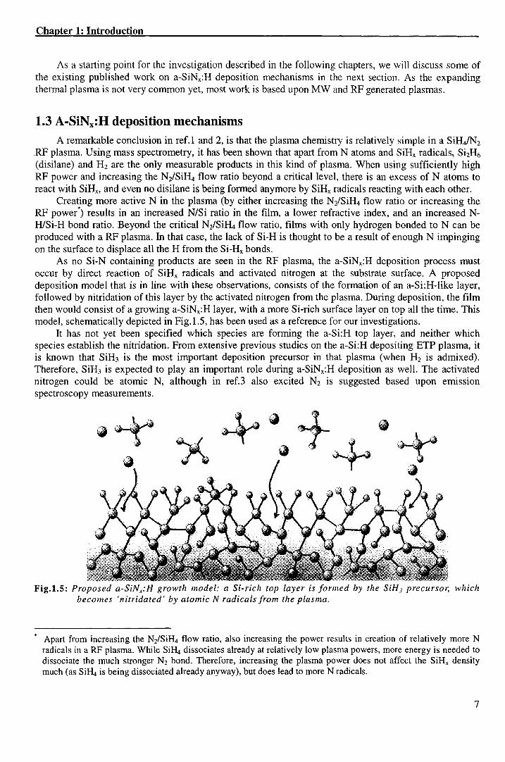
As no Si-N containing products are seen in the RF plasma, the a-SiNx:H deposition process must occur by direct reaction of SiHx radicals and activated nitrogen at the substrate surface. A proposed deposition model that is in line with these observations, consists of the formation of an a-Si:H-like layer, foliowed by nitridation of this layer by the activated nitrogen from the plasma. During deposition, the film then would consist of a growing a-SiNx:H layer, with a more Si-rich surface layer on top all the time. This model, schematically depicted in Fig.l.5, has been used as a reference for our investigations.
lt has not yet been specified which species are forming the a-Si:H top layer, and neither which species establish the nitridation. From extensive previous studies on the a-Si:H depositing ETP plasma, it is known that SiH3 is the most important deposition precursor in that plasma (when H2 is admixed). Therefore, SiH3 is expected to play an important role during a-SiNx:H deposition as wel!. The activated nitrogen could be atomie N, although in ref.3 also excited N2 is suggested based upon emission spectroscopy measurements.
Fig.l.S: Proposed a-SiNx:H growth model: a Si-rich top layer is formed by the SiH3 precursor, which becomes 'nitridated' by atomie N radicals from the plasma.
Apart from increasing the Nz/SiH4 flow ratio, also increasing the power results in creation of relatively more N radicals in a RF plasma. While SiH4 dissociates already at relatively low plasma powers, more energy is needed to dissociate the much strenger N2 bond. Therefore, increasing the plasma power does not affect the SiHx density much (as SiH4 is being dissociated already anyway), but does lead tomoreN radicals.
7
Plasma and in situ film studies on silicon nitride growth for photovoltaic applications
In the next section, the steps that are taken to verify the model are discussed, and an overview of the contents of this report is given.
1.4 Goal of this investigation and outline of the report To determine if the discussed model is applicable for the ETP process, the plasma species that are
involved in this model are investigated. The SiH3 and SiH densities in the plasma have been measured using cavity ringdown spectroscopy (CRDS), and the N radical density has been measured using threshold ionization mass speetrometry (TIMS). Also, an attempt is made to measure H. It is verified whether the measured radical densities are high enough to explain the film deposition rate.
Parallel to the plasma investigations, the deposited films have been investigated using attenuated total reflection (ATR) infrared spectroscopy, a for this purpose newly installed technique. Using this technique, the infrared absorptions of SiHx, NHx and SiN honds have been foliowed in as-deposited aSiNx:H films. An attempt to find more evidence for the proposed deposition mechanism is made, by verifying whether a-SiNx:H can indeed he created by 'nitridation' of a-Si:H, by exposing an a-Si:H film to a N-containing plasma.
In chapter 2, the relevant theory behind the three used measurement techniques CRDS, TIMS and ATR-FTIR spectroscopy, and the foliowed measurement procedures are described in detail. In chapter 3 the measured radical densities in respectively the non-depositing souree plasma (before SiH4 injection), and the depositing plasma are presented, as well as an estimate of the contribution to the film growth of each radical. In chapter 4, an in situ film study with use of the A TR technique is presented. Measured SiH and NH densities in different types of a-SiNx:H films are discussed, as well as the mentioned nitridation expetiment. Finally, in chapter 5 a number of conclusions are drawn.
8
Chapter 2: Plasma and surface measurement technigues: Cavity ringdown spectroscopy
Chapter 2
Plasma and surface measurement techniques
In this chapter, three of the measurement techniques that have been used are presented, as well as the foliowed measurement procedures. To measure the densities of radical species in the plasma during the aSiNx:H deposition process, both cavity ringdown spectroscopy (CRDS) and threshold ionization mass speetrometry (TIMS) have been used. The CRDS technique is well described elsewhere, so just a brief introduetion to the general technique is given in section 2.1, along with the used theory and followed procedures to measure SiH and SiH3 in the a-SiNx:H depositing plasma. The TIMS measurement procedure is not as common in the group yet, and is therefore described more in depth in section 2.2, on the basis of the density measurement procedure of atomie N. In section 2.3, the newly set-up attenuated total reflection fourier transfarm infrared spectroscopy (ATR-FTIR) technique is explained, and a description of the specific used setup is given.
2.1 Cavity ring down spectroscopy (CRDS): SiH and SiH3 radical density CRDS measurements have been carried out of both the SiH and SiH3 radical densities in the a-SiNx:H depositing Ar/H2/N2/SiH4 plasma. These radicals have been measured previously in the a-Si:H depositing plasma4
·5
. The measurement procedure is described in detail in ref.6, and therefore here only a short overview of the technique is given, together with the specific experimental details.
2.1.1 The basicsof CROS
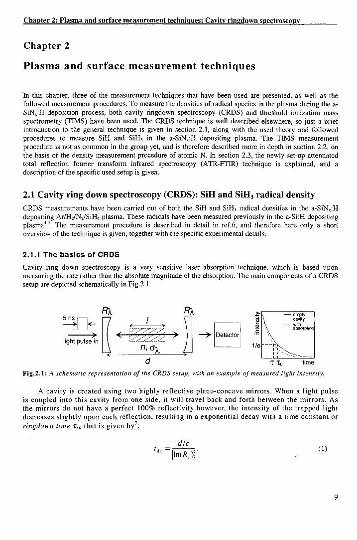
Cavity ring down spectroscopy is a very sens1t1ve laser absorption technique, which is based upon measuring the rate rather than the absolute magnitude of the absorption. The main components of a CRDS setup are depicted schematically in Fig.2.1.
d
\ 1/e --r.
I î,
- empty cavity
-·- with absorption
I I '·. '·
1: 1:0 time
Fig.2.1: A schematic representation of the CRDS setup, with an example of measured light intensity.
A cavity is created using two highly reflective plano-concave mirrors. When a light pulse is coupled into this cavity from one side, it will travel back and forth between the mirrors. As the mirrors do not have a perfect 100% reflectivity however, the intensity of the trapped light decreases slightly upon each reflection, resulting in a exponential decay with a time constant or ringdown time 'Z",1.o that is given b/:
djc r J.o = IIn(R" )I ,
(1)
9
Plasma and in situ film studies on silicon nitride growth for photovoltaic applications
with d the distance between the mirrors, c the speed of light, and R;.. the mirror's reflectivity. This decaying light intensity is measured using a detector that collects the amount of light that is transmitted from the cavity at the second mirror. The ringdown time r;..0 is determined by fitting linear functions to the natura! logarithm of the measured signa! after each light pulse. The ringdown time is averaged over typically 64 laser shots.
When an absorbing medium (in our case: the studied plasma) is placed between the mirrors in the cavity, the light intensity decreases more rapidly due to the absorption. The ringdown time is then given b/:
(2)
with A;. the absorption per pass for the laser wavelength A used*. The absorption per pass A;. by the plasma can be deduced from equation (1) and (2):
(3)
As visible, neither the mirror reflectivity nor the laser light intensity has to be known to obtain the absorption per pass A;..
Finally, to convert a measured absorption A;. to a density, the wavelength dependent cross section a;. and the density profile of the plasma has to be known. When assuming a cylindersymmetrie profile of the plasma, the density profile at a certain distance from the souree can be obtained from a radial scan of the absorption using Abel inversion. For simplicity however, a cylindrical plasma with homogeneaus density over a diameter length I is often assumed. In that case, the density n can be obtained from
(4)
2.2.2 CROS on SiH3
In the next sections, the experimental details of the SiH3 measurements are treated. In section A, the relevant spectroscopy of SiH3 is treated, foliowed by the measurement procedureinsection B.
A. SiH3 spectroscopy For the SiH3 density measurement, -215 nm light is used to measure the electronic transition8
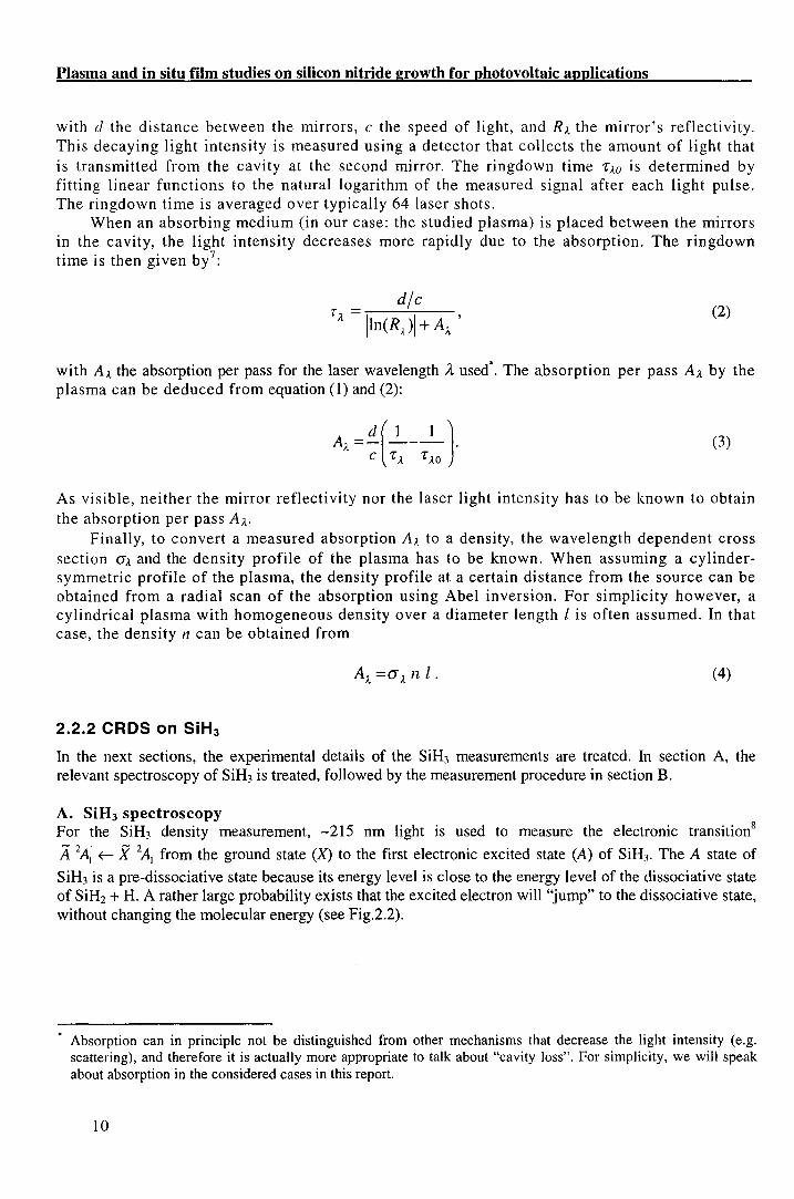
A 2A; ~ X 2A1 from the ground state (X) to the first electronic excited state (A) of SiH3• The A state of
SiH3 is a pre-dissociative state because its energy level is close to the energy level of the dissociative state of SiH2 + H. A rather large probability exists that the excited electron will "jump" to the dissociative state, without changing the molecular energy (see Fig.2.2).
Absorption can in principle not be distinguished from other mechanisms that decrease the light intensity (e.g. scattering), and therefore it is actually more appropriate to talkabout "cavity loss". For simplicity, we will speak about absorption in the considered cases in this report.
10
Chapter 2: Plasma and surface measurement technigues: Cavity ringdown spectroscopy
!? (]) c (])
~ ë (]) -0 a.
intramolecular distance
Fig.2.2: Schematic potenrial energy diagram, illustrating the possibility of dissociation of SiH3. The electronic transition from the X to the A state, and the following dissociation are indicated with arrows. 6
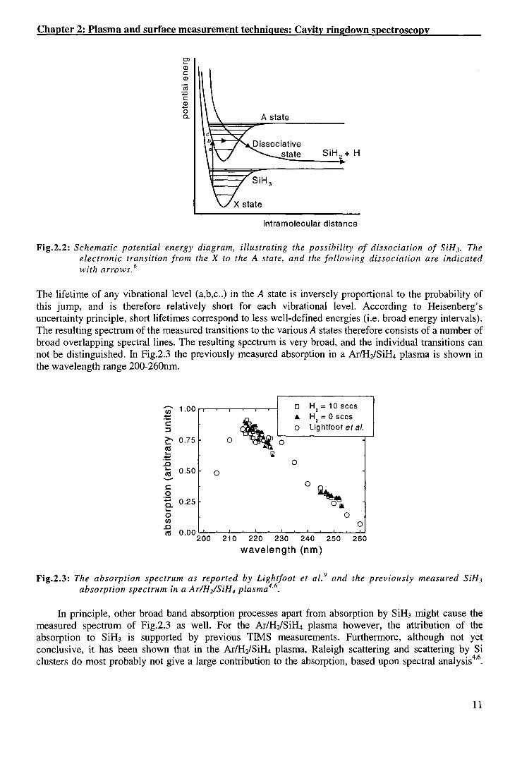
The lifetime of any vibrational level (a,b,c .. ) in the A state is inversely proportional to the probability of this jump, and is therefore relatively short for each vibrational level. According to Heisen berg' s uncertainty principle, short lifetimes correspond to less well-defined energies (i.e. broad energy intervals). The resulting spectrum of the measured transitions to the various A states therefore consists of a number of broad overlapping speetral lines. The resulting spectrum is very broad, and the individual transitions can not be distinguished. In Fig.2.3 the previously measured absorption in a Ar/H2/SiH4 plasma is shown in the wavelength range 200-260nm.
en 1.oo ::: c :l
è' 0.75 (\3 .... ::: .0 ~ 0.50 -c 0 Ë. 0.25 .... 0 rn .0 (\3 0.00
200
0
0 H2 = 10 sccs
'0 • H
2 = 0 sccs
0 Lighttoot et al.
0
lil 0
0
'~ Oa 0
0
210 220 230 240 250
wavelength (nm) 260
Fig.2.3: The absorption spectrum as reported by Lightfoot et al. 9 and the previously measured SiH3
absorption spectrum in a Ar/H2/SiH4 plasma4·6
•
In principle, other broad band absorption processes apart from absorption by SiH3 might cause the measured spectrum of Fig.2.3 as well. For the Ar/Hz/SiH4 plasma however, the attribution of the absorption to SiH3 is supported by previous TIMS measurements. Furthermore, although not yet conclusive, it has been shown that in the Ar/H2/SiH4 plasma, Raleigh scattering and scattering by Si clusters do most probably not give a large contribution to the absorption, based upon speetral analysis4"6.
11
Plasma and in situ film studies on silicon nitride growth for photovoltaic applications
Although the spectrum has just been measured at one point in the a-SiNx:H depositing Ar/H2/N2/SiH4
plasma so far, we assume for the moment that this is true for this plasma as wel!.
B. SiH3 Measurement procedure In the used setup (see Fig.2.1), the light pulses are generated using a tunable dye laser (Sirah Precisionscan-D), pumped by a Nd: Y AG laser (Spectra-Physics Quanta Ray DCR-11 ). Also a filter is used to reduce the light intensity. The rnirrors (which simultaneously act as vacuum seals) are positioned at a distance d of 1.08m from each other. The light that leaks out of the cavity is filtered again using a band pass filter. As light detector a photo multiplier tube (PMT) is used.
For the measurement of the SiH3 density in the Ar/H2/Nz/SiH4 plasma, the braadband absorption is measured over a small range at its maximum around 215 nm. Mirrors with a reflectivity of -96% around 215 nm have been used. For estimating the density n with equation (4), a cross section a of 2.4·10-21 m2 at 215 nm is used as given by Lightfoot et a/. 9
• The rnirror distance dis 1.08m, and a plasma diameterlof 0.40m is used*.
2.2.3 CROS on SiH
In this section, the experimental details of the SiH measurements are treated. In section A, the relevant spectroscopy of SiH is treated. In sections B and C, the measurement procedure and rotational and vibrational temperature measurements are explained. In the following sections D and E, the measured spectra and background absorptions are discussed.
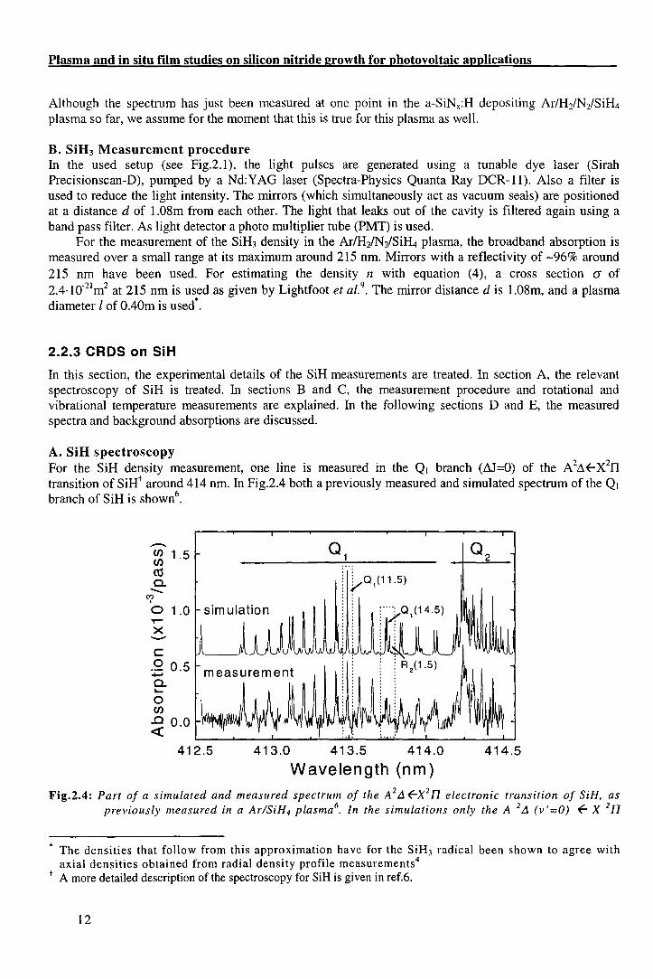
A. SiH spectroscopy For the SiH density measurement, one line is measured in the Q 1 branch (LV =0) of the A 2LH-X 2n transition of SiHt around 414 nm. In Fig.2.4 both a previously measured and simulated spectrum of the Q1
branch of SiH is shown6.
-~ 1.5 ces Cl. -C'(
0 1.0 T"'
x
c .Q 0.5 -Cl. ~
0 en .0 0 0 <('
maasurement
~
j J,-a 1(11.5)
:····: Q (14.5) :/1
412.5 413.0 413.5 414.0
Wavelength (nm) 414.5
Fig.2.4: Part of a simulated and measured spectrum of the A 2 Ll t=-X2 n electron ie transition of SiH, as previously measured in a Ar!SiH4 plasma6
. In the simulations only the A 2 Ll (v '=0) t=- X 2 n
• The densities that follow from this approximation have for the SiH3 radical been shown to agree with axial densities obtained from radial density profile measurements4
t A more detailed description of the spectroscopy for SiH is given in ref.6.
12
Chapter 2: Plasma and surface measurement techniques: Cavity ringdown spectroscopy
(v"=O) hand is taken info account. In this work, the rotationalline Qt(//.5) is used to determine the SiH density and the relative height ofQJ(14.5) and R2(1.5) absorptions are used todetermine the rotational temperafure (for one plasma condition only).
The various absorption peaks in this branch correspond to the different rotational states of the radical, and are labeled according to the rotational quanturn number J of each state. The amount of absorption A~ depends on the density n of SiH in the specific corresponding state, integrated over the pathway l through the plasma, and the cross section <1A. for the corresponding transition. If we again assume a homogenous plasma density, the density of one particular state can be obtained from equation (4). As the absorption is integrated* over the peak, also an integrated cross section <1.1. is used, which is obtained from
(5)
with À;k the wavelength of the transition from level i to k, and h Planck's constant. B;k is the Einstein absorption coefficient that is obtained from the program LIFBASE10
, for simulating spectra of diatomic molecules.
The total ground state density is the sum of the densities of each rotational state. One way to determine the total ground state density would be by scanning a complete rotational transition branch. In practice however, only one rotational state density (i.e. one peak) is measured for each plasma condition. To deduce the total ground state density from the density of this particular state, a calculation6 is made of the relative occupation distribution of all rotational and vibrational states in the ground state. This distribution depends on the vibrational and rotational temperature. In our case, a Boltzmann distribution over the various rotational state densities is assumed.
B. Measurement procedure For the SiH measurements, the same setup as for the SiH3 measurements is used. Mirrors with a reflectivity of 99.6% around 414 nm have been used. The Q1(11.5) SiH peak is measured at 413.5 nm, as indicated in Fig.2.4.
An example of an absorption spectrum is shown in Fig.2.5. The scans are measured from higher to lower wavelengths. The ring down time of the non-absorbing Ar/H2 plasma is used as baseline to determine r0 (equation (3)).
• Integrated absorptions (i.e. peak areas) are used rather than the absorptions at one wavelength, as the height/width of a peak depends on the temperature (Doppler broadening) and the line profile of the laser.
13
Plasma and in situ film studies on silicon nitride growth for photovoltaic applications
-'<t 14 'o unknown T'"'" peaks ..._
12 ct1
~~ E 10 + N2 CJ) I ct1 c.. 8 (J) + SiH
4 ..c 6 ->- 4 I AriH, ..c c plasm 0 2 I -c.. ~ 0 0 CJ)
..c 413.56 413.58 413.60 413.62 <(
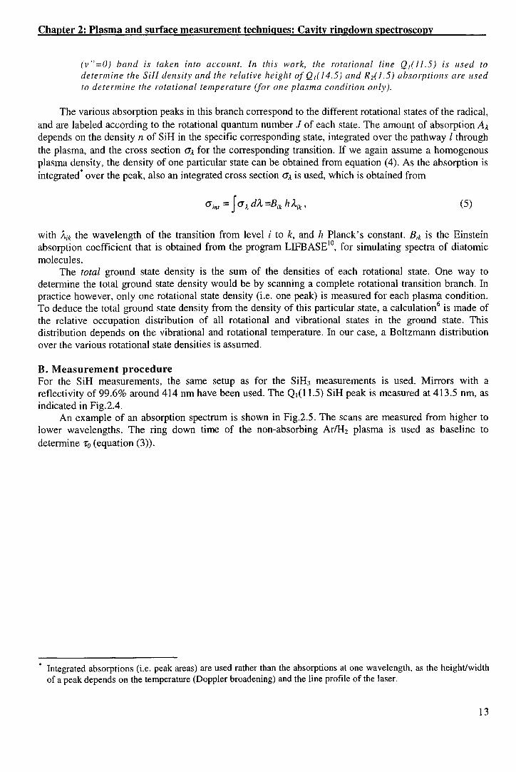
Wavelength (nm) Fig.2.5: Absorption spectrum during a-SiNx:H depositing plasma (Ar flow 55, H2 5, N2 8, SiH4 4 sccs,
are current 45 A). Around 413.6 nm both the Qd 11.5) peak and extra unidentified peaks are visible. Furthermore, there is a braadband background absorption, which increases when N2
is admixed to the plasma. The measured spectrums feature a shift in wavelength of about 1 nm (which is corrected for in the plot) and an erroneous wavelength scale factor, due to the alignment of the specific laser setup. By camparing a measured SiH spectrum to a simulated spectrum, a sealing factor of 1.174 has been estimated, which has been used to scale down the fitted peak areas.
A number of aspects are visible in the spectrum: • The Q1(11.5) peak around 413.5 om is present. The surface ofthis peak is the integrated absorption A-1.
which is used in equation (5) to calculate the density of this SiH state. • At least two extra absorption peaks are present next to the SiH peak. These peaks are of yet unknown
origin. • Apart from the peak absorptions, also a braadband absorption by the plasma occurs in this wavelength
range when silane and nitrogen are fed into the plasma.
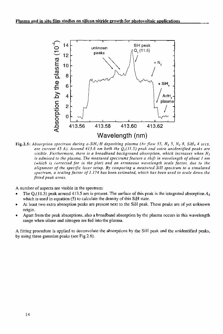
A fitting procedure is applied to deconvolute the absorptions by the SiH peak and the unidentified peaks, by using three gaussian peaks (see Fig.2.6).
14
Chapter 2: Plasma and surface measurement technigues: Cavity ringdown spectroscopy
13
12 -"<t
'o ,.- 11 x -c 10 0
:,::::; 9 a.
1-0 (/) 8 .n <(
7 .. ~~··:.:
SiH peak 01(11.5)
\
413.58 413.59 413.60 413.61 Wavelength (nm)
Fig.2.6: Deconvolution of the measured SiH and unknown peaks.
C. Rotational and vibrational temperature, and relative state occupation As mentioned, to obtain the total ground state density from a single measured rotational state density, the rotational and vibrational temperatures have to be known.
One way to estimate the rotational temperature in the plasma, is by comparing the relative height of the various absorption peaks in a measured spectrumtoa simulated spectrum, using LIFBASE10
. Again, to save time, just a small part of the spectrum is measured. In our case, the Q1(14.5) and R2(1.5) rotational transition peaks are compared (as indicated in Fig.2.4), which have a relative height that varles strongly with the rotational temperature. For the plasma condition with flow rates Ar 55 sccs, SiH4 8 sccs, N2 10 sccs, H2 5 sccs and are current 45A, a rotational temperature of 1400K has been estimated in this way.
The vibrational temperature is not measured in the a-SiNx:H depositing plasma. In the a-SiHx depositing plasma however a vibrational temperature of -3000K is measured 11
, by optical ernission spectroscopy (OES). As the relative state occupancy does not depend strongly on the vibrational temperature anyway, this value is taken as an approximation.
These temperatures and the assumption of a Boltzmann distribution have been used to calculate the relative rotational state occupancies in the SiH ~round state. For the 1=11.5 groundstate a relative accupation of 1.97% has been estimated in this way .
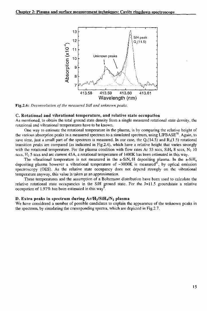
D. Extra peaks in spectrum during Ar/H2/SiH4/N2 plasma We have considered a number of possible candidates to explain the appearance of the unknown peaks in the spectrum, by simulating the corresponding spectra, which are depicted in Fig.2.7.
15
Plasma and in situ film studies on silicon nitride growth for photovoltaic applications
413.44 413.46 413.48 413.50 413.52
wavelength (nm) Fig.2.7: A comparison between the Qd 11.5) SiH peak + unknown peaks as measured in a Ar/H2/N2/SiH4
plasma, and simulated spectra of SiN, N2 + and SiH10•
• SiN: As the extra peaks are only present when both SiH4 and Nz are fed into the plasma, SiN seems a good candidate. The simulated spectrum of SiN does however notmatch the measured extra peaks.
• N/: N/ has been a promising candidate, as its absorption spectrum has peaks in the 414 nm region and even one peak on the exact position of our peak. However, the N2+ spectrum does not fully coincide with the measured spectrum.
• SiH: Another considered possibility is the formation of higher excited vibrational states ("hot bands") of SiH, that might he created in areaction path involving nitrogen. LIFBASE is used to calculated the possible transitions from v"= 0,1,2,3 to v'=0,1,2. Again, the extra absorption peaks in the vicinity of the Q1 peak do notmatch the measured spectrum. The mentioned observation that the peaks are only present when both SiH4 and Nz are fed into the plasma, already makes N2+ and SiH less probable candidates anyway.
E. The broadband absorption a-Si:H plasma: A broad band absorption at the 414 nm region has been observed earlier12 in the a-Si:H depositing (Ar/H2/SiH4) plasma. Of the various candidates for this absorption, the possibility of Raleigh scattering and absorption by Si clusters is thought to he unlikely in that plasma, based upon the measured wavelength dependence, although this is not conclusive. Some correlation to the measured SiH3 density has been observed. Therefore, the background absorption in the a-Si:H depositing plasma could he caused by a species in the plasma, of which the production mechanism is related to the SiH3 density. a-SiNx:H plasma: When Nz is added to the plasma, an increase by a factor of -3 of the absorption level occurs (see Fig.2.5). The absorption increases with either both increasing Nz or SiH4 flows, and decreases slightly with increasing Hz flow. Again, for SiH4 and Hz flow variations, this trend is observed for SiH3 in the a-SiNx:H depositing plasma as well (the SiH3 density has not been measured as function of the N2 flow rate). Possible candidates are broadband absorption by electron detachment processes from negative i ons, which probably have a too low cross section a-1 o-zz m2 to explain the large absorption, and excitation to a pre-dissociative state similar to the SiH3 case.
16
Chapter 2: Plasma and surface measurement techniques: Threshold ionization mass speetrometry
2.2 Threshold ionization mass speetrometry The plasma density of atomie N has been measured using a mass spectrometer. Measuring radical
species using a mass spectrometer requires a specific approach, which is usually referred to as threshold ionization mass speetrometry (TIMS), or in some cases as appearance potential mass speetrometry (APMS). After an introduetion on quadrupale mass speetrometry in generaland our setup specifically, the TIMS technique and the particularly used method to measure and analyze the spectra adapted from ref.l3 will be treated in this section.
2.2.1 Quadrupele mass speetrometry
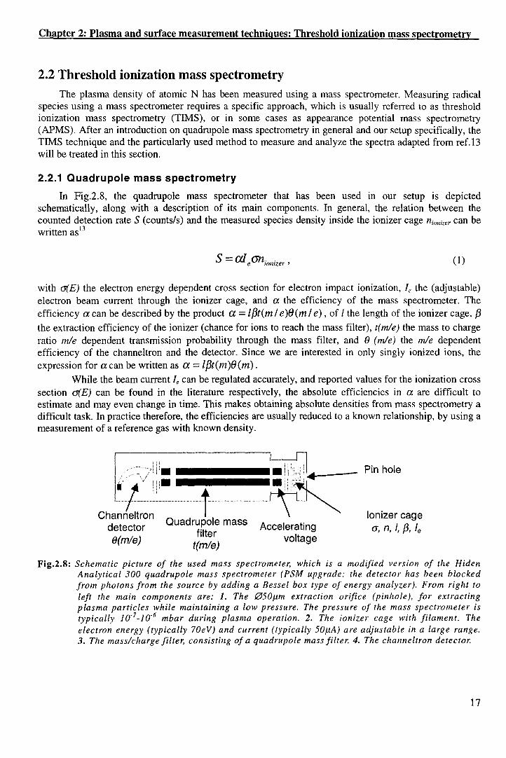
In Fig.2.8, the quadrupale mass spectrometer that has been used in our setup is depicted schematically, along with a description of its main components. In general, the relation between the counted detection rate S (counts/s) and the measured species density inside the ionizer cage n;onizer can be written as 13
S =aleanionizer • (I)
with CJ(E) the electron energy dependent cross section for electron impact ionization, Ie the (adjustable) electron beam current through the ionizer cage, and a the efficiency of the mass spectrometer. The efficiency a can bedescribed by the product a= l/3t(m/ e)(j(m/ e), of l the lengthof the ionizer cage, f3 the extraction efficiency of the ionizer (chance for ionstoreach the mass filter), t(mle) the mass to charge ratio mie dependent transmission probability through the mass filter, and (:} (mie) the mie dependent efficiency of the channeltron and the detector. Since we are interested in only singly ionized ions, the expression for acan be written as a= lf3t(m)(j(m).
While the beam current Ie can be regulated accurately, and reported values for the ionization cross section CJ(E) can be found in the literature respectively, the absolute efficiencies in a are difficult to estimate and may even change in time. This makes obtaining absolute densities from mass speetrometry a difficult task. In practice therefore, the efficiencies are usually reduced to a known relationship, by using a measurement of a reference gas with known density.
:"lil. ====•W, *f Pl. _J ______ M~~ Channeltron I \
detector 8(m/e)
Quadrupele mass Accelerating filter voltage
t(mle)
Pin hole
lonizer cage G, n, I, {3, Ie
Fig.2.8: Schematic picture of the used mass spectrometer, which is a modified version of the Hiden Analytica/ 300 quadrupale mass spectrometer (PSM upgrade: the detector has been blocked from photons from the souree by adding a Besset box type of energy analyzer). From right to left the main components are: I. The 050pm extraction orifice (pinhole), for extracting plasma particles while maintaining a low pressure. The pressure of the mass spectrometer is typically 10·7-10·6 mbar during plasma operation. 2. The ionizer cage with filament. The electron energy (typically 70eV) and current (typically 50pA) are adjustable in a large range. 3. The mass/charge filter, consisring of a quadrupale mass filter. 4. The channeltron detector.
17
Plasma and in situ film studies on silicon nitride growth for photovoltaic applications
2.2.2 Beam and background density
The density of species in the ionizer cage nionizer is a sum of the beam (or 'line of sight') component of species extracted from the plasma, and the background contribution
nionizer=nBeam+ nBackground · (2)
lt is important to notice that of both contributions, only the beam component is directly proportional to the species density in the plasma. The detection rate of the beam component is proportional to the plasma density, because densities ins i de the ionizer cage determine the detection rate, rather than partiele fluxes. Although the flux through the pinhole is generally higher for faster (lighter) particles, the residence time of these particles spent in the ionizer cage is inversely proportional to their velocity. On the other hand, the background density (i.e. the density of particles that are allowed to re-enter the ionizer cage) does depend on the incoming flux and the pumping speed of the specific species. In the case of radical species, also the wall recombination probability y of the specific radical strongly influences the background density.
Methods to separate the beam signa! from the background include beam modulation (e.g. by chopping), and multi-stage differential pumping. As our setup however is (yet) not equipped with either of both, a proportionality factorCis introduced given by1 1
c = 11beam + 11
backJirt!lll!d '
11beam
(3)
to account for the increased density inside the ionizer cage. On the basis of the geometry of our specific setup, C is estimated to be -35 for non-radical species with a wall loss probability y of 0, assuming a pumping speed of 50-60 l/s11
• However, for radical species that do have a wallloss probability y.>O, C will have a smaller value, decreasing to 1 for radicals with unit wallloss probability }'= 1.
2.2.3 Radical density measurement: threshold ionization mass speetrometry
While the discussion in the previous section mostly applies to mass speetrometry in genera!, the measurement of radicals involves a specific approach. In this section, radical density measurement using threshold ionization mass speetrometry (TIMS) is explained by using the example of N-radical measurements, as performed for this study.
Typically applied electron i ooization energies in mass speetrometry ( -70e V) are high enough for the dissociation (cracking) and ionization of any molecule from the plasma. With these energies therefore, it is not possible to measure radical densities in the plasma, as the directly ionized radicals can oot be distinguished from identical radicals that are created by dissociative ionization of their parent molecules. As radicals are often present in much lower density than their parent molecules, their detection rate would in many cases be drowned by the detection rate of their cracked parents.
To get round this problem, TIMS utilizes the energy difference (typically >2eV) that exists between the ionization energy threshold of a radical (Ei) and the dissociative ionization energy threshold of its parent molecule (E0 ). Por instance, there is a lOeV gap between the thresholds of ionization of atomie N and dissociative i ooization of N2:
N+e => W+2e N2 + e => W + N + 2e
Ei= 15.18 eV Ea = 25.26 eV
When using ionization energies between both ionization energy thresholds, just the N radicals from the plasma cao be ionized and detected while the parent molecules are left intact. This is demonstrated in
18
Chapter 2: Plasma and surface measurement technigues: Threshold ionization mass speetrometry
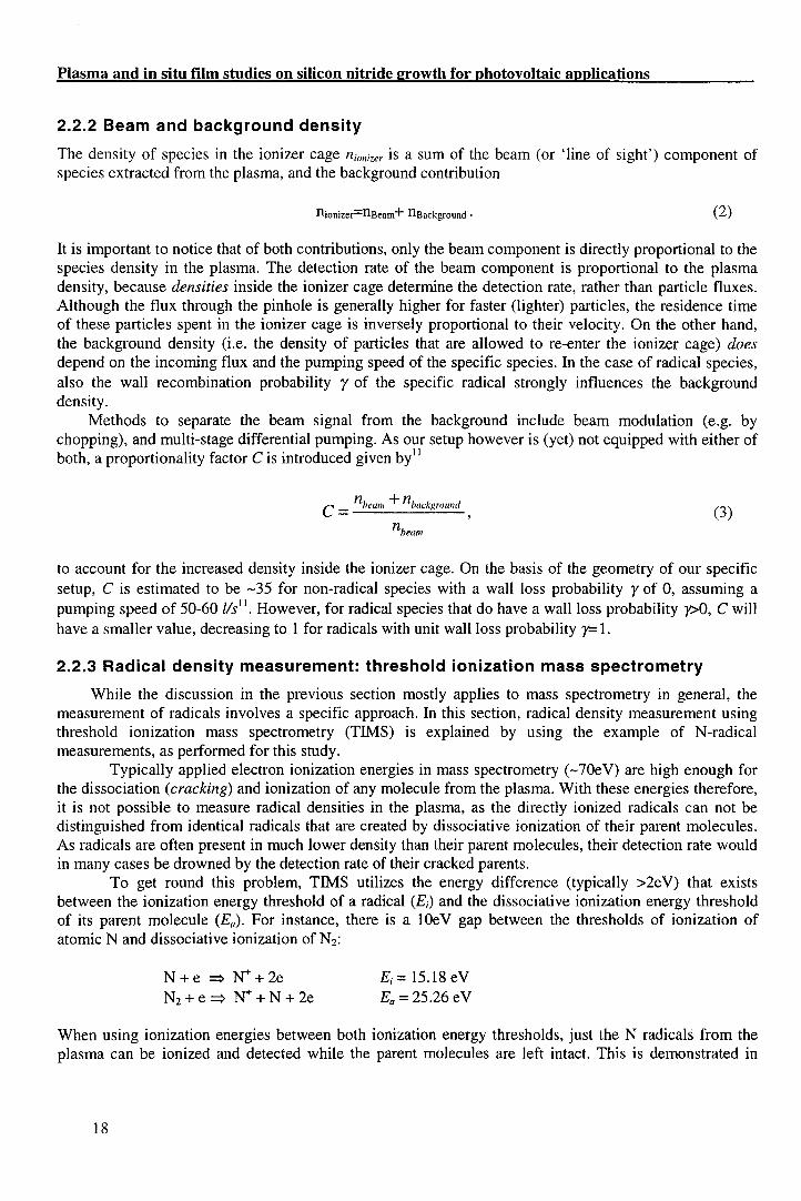
Fig.2.9, in which an electron energy scan of the detection rate at 14 amu (the mass of atomie N) is shown, both during an Ar/N2 plasmaand with the plasma turned off at constant gas flows.
"0 § 1000 0 Q)
---- Plasma on -- Plasma off
N + e => N+ + 2e ~ (E h 1d=15.18 eV) Q) 1 OO thres o
a. (/) -c :::J 0 0
::t:l::
10
\ 1
This signal is due to pyrolysis
15 20 25 30 35 tonization energy (eV)
Fig.2.9: Detection rate of N in an Ar/N2 plasma vs. the ionization energy, bothfor plasma turned on and off
Two regions are visible in the measured detection rates of N in Fig.2.9. From 15.18 eV only N radicals from the plasma are ionized and detected, while from 25.26 eV an additional signal due to N radicals created by dissociative ionization of N2 can be seen. Therefore, the detection rate in region 1 is used for obtaining the density of N radicals.
However, when the plasma is turned off (also shown in Fig.2.9), there still is a small detection rate left. This is attributed to radicals created by thermal dissociation (or pyrolysis) of N2 close to the filament. Naturally, this additional souree of radicals is present during plasma operation as well. Therefore, to correct for this pyrolysis contribution to the signal, the count rate after turning the plasma off (at constant gas flows) is subtracted from the count rate during plasma on. But, as visible in the second region, the N2
density is higher when the plasma is off, because of a lower gas temperature and the absence of gas consumption. Therefore the plasma off pyrolysis signal is scaled down first, using the ratio of the detection rates at high ( -70 e V) ionizing energies during the plasma turned on and turned off respecti vely. For this sealing factor, it is assumed that the N density is much smaller than the N2 density, such that the plasma N radical signa! becomes negligible compared to the N2 signal at high ionization energies. To summarize, the plasma radical signa! Sis corrected for the pyrolysis contribution using the equation:
S S?OeV,plasma_on S Plasma radica/ = l5-25eV,plasma_on- S
?Oe V, plasma _ (!tf . Sl5-25eV,plasma_(1{( (4)
It should be noted that in the case of N, the contribution of pyrolysis to the radical count rate is relatively small due to the high N2 bond strength. Having obtained the detection signal of plasma N radicals, the next step is to obtain a density from this signal, which is discussed in the next section.
19
Plasma and in situ film studies on silicon nitride growth for photovoltaic applications
2.2.4 Converting detection rates to densities
:ê'6o 2 f· § 50 0 2,.40 Q)
a; 30 '-
§ 20
ü Q) 10 -Q)
I N detection ra te .>/- /
.\//;/// / :! ·, '/i 1':
//;· I _.,, I'
:' /'
"0 0 z
,;\JY ,/---Ar detection ra te
''-"'·"-'-"-~' ·--------1' 12 14 16 18 20 22
Electron energy (eV)
~
3~ (!)
2~ 0
"' 1 (") 0 c
0:::::1 -en 24 èn -
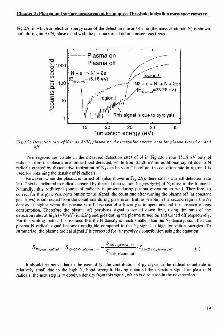
Fig.2.10: Measured N and Ar defection rates vs electron energy, linear scale. The energy scale has been calibrated using the ionization threshold of Ar (40 amu) at 15.7 eV, which is always present in the studied processes.
In figure I 0, measured N detection and Ar detection rates are shown, close to their respective ionization threshold energies. As visible, both detection rates are nearly proportional to the electron energy. It is in fact generally observed that ju st above the threshold energy, the electron impact ionization cross section is to a good approximation a linear function of the electron energy:
ax~x· = Àx~x· (E _ E,7,,.:;,:,;J, (5)
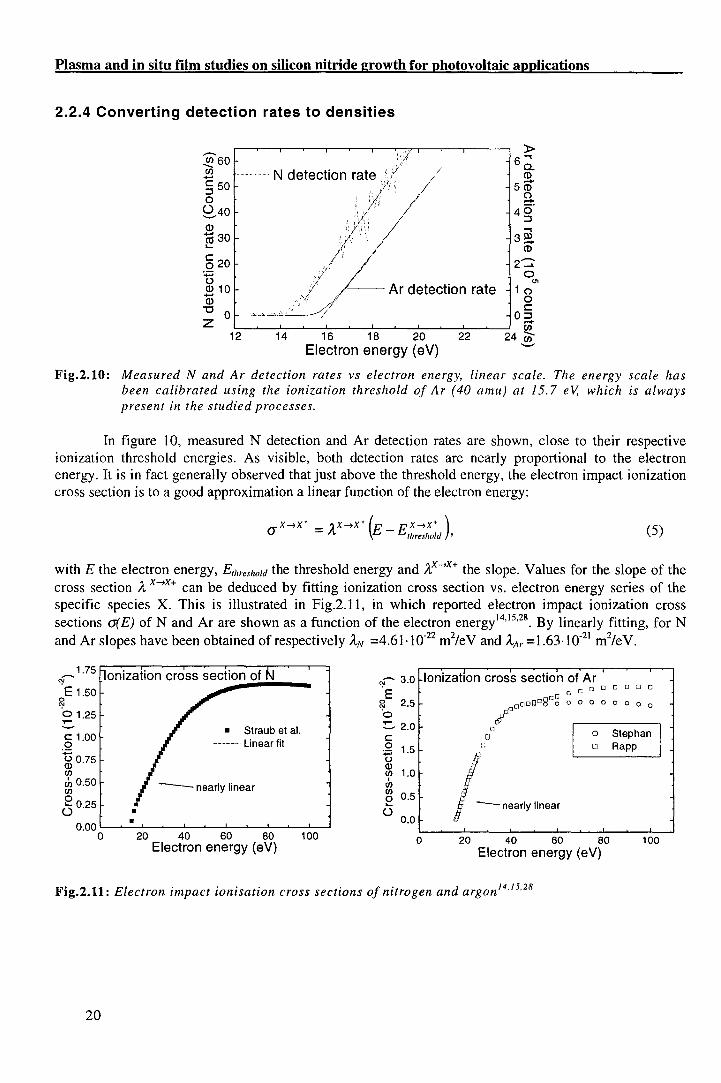
with E the electron energy, Erhre.~hotd the threshold energy and Àx~x+ the slope. Values for the slope of the cross section À x~x+ can be deduced by fitting ionization cross section vs. electron energy series of the specific species X. Th is is illustrated in Fig.2.11, in which reported electron impact ionization cross sections a( E) of N and Ar are shown as a function of the electron energy 14
'15
'28
. By linearly fitting, for N and Ar slopes have been obtained of respectively ÀN =4.61-1 o·22 m2/e V and ÀA,. =1.63-1 0"21 m2/e V.
_1.75 ')I
E 1.50 ~ 01.25 T""
c: 1.00 0
~0.75 en u, o.5o en 0 00.25
lonization cross section of N
• •
• Straub et al. ----·-- Linear fit
0.00 '---~--'--~-'-~--'-----'-----''---~--'----' 0 20 40 60 80 100
Electron energy (eV)
')'- 3.0 lonizat1on cross section of Ar c c 0 0 0
occ .. 0 0 0
E 0 ')I 0
2.5
:::.. 2.0 c ~ 1.5 (J
~ 1,0 I en ~ 0.5 .... ()
0.0
0
000 ogc 0 o o o o o o
rl' 0 0 0
L1 ÇJ
[J I o Stephan I D Rapp
20 40 60 80 100 Electron energy (eV)
F . 2 11 El . . . . . 1 . d 14 15 28 1g. . : ectron tmpact wnzsatwn cross sectwns o nltrogen an argon · ·
20
Chapter 2: Plasma and surface measurement techniques: Threshold ionization mass speetrometry
By substituting the equation for the cross section (5) in the equation for the detector count rate (I), we can write for the relation between ionizer density and detection rate:
n .. =----wmzer aJ A X ~x+ '
e
(6)
in which Ax~x+ is (analogously to À X-7X+) defined as the slope of the measured detection rate close to the ionization threshold. As already mentioned in section 2.2.1 however, the extraction efficiency {3, mass filter transmittance t(m) and channeltron detector efficiency 8(m) that determine the overall mass spectrometer efficiency a, are unknown. Therefore, usually a known reference density is measured as well. One previously often used species as reference, is the radical parent molecule. The radical parent can be measured with unchanged mass spectrometer settings by just increasing the electron energy beyond the threshold for dissociative ionization. E.g. in the case of N measurements, the parent molecule N2 is dissociatively ionized into W. With this approach, {3 and 8(m) are supposedly totally eliminated as the samepartiele (e.g. N+) passes through the mass filter and detector.
However, recently Harmeet Singh et al. 13 pointed out that in comparison to "normal" ionization, the extraction efficiency {3 could be 2 to 50 times smaller for dissociatively ionized particles due to a totally different velocity distribution after ionization, due to the Frank Condon effect. To eliminate {3, the reference gas should be measured using "normal" ionization instead of dissociative ionization. An equal extraction efficiency {3 u pon (non-dissociative) ionization has in deed been reported 13 for a large number of gases, among which Ar, H2, N2, C02, 02.
As Ar gas is always present in the plasma processes under study, the Ar density (with plasma power turned off) is used as the reference. Using equation (6), the measured radical density in the plasma n""x can be expressed with the measured signa! slopes AX-7X+ (plasma on), AAHAr+ (plasma off) and the Ar reference density n°11~r as:
(7)
Still left are the mass filter transmission t(m) and channeltron/detector efficiencies 8(m). For the product of both t(m)8(m), a m·1 dependenee has been measured20'23
, which has been used in the calculations.
2.2.5 Further experimental details for the N radical measurements
Por each measured plasma condition, 4 ionization energy scans are made, which are listed in table 1. These scans are repeated during plasma off to obtain the detection rate of the Ar reference density, as well as the correction for pyrolysis.
Table 1: Mectsurement procedure
Partiele Mass looization threshold Energyscan A N~W 14amu 15.18 eV 14-35 e V -7 plasmaN radicals + pyrolysis B N2~w 25.26 eV 68-72 eV -7 dissociatively ionized N2
c Ar~ Ar+ 40amu 15.7 eV 14-22 eV -7 Ionized Ar close to threshold 7J 68-72 e V -7 not used for the N measurements
With these measurements and equation (7), the density of N inside the mass spectrometer ionizer cage can be obtained, with respect to the Ar density inside the ionizer cage.
21
Plasma and in situ film studies on silicon nitride growth for photovoltaic applications
Unfortunately however, the ratio of the densities in the ionizer cage is not necessarily equal to the ratio of densities in the plasma, as follows from the discussion in section 2.2.2 on the beam and background densities in the mass spectrometer. While Ar does nat get lost to the steel walls of the mass spectrometer, the N radicals do have a probability to recombine at the surface. In Fig.2.12, two reported measurements of the recombination probability of atomie N on steel are shown, in two different pressure ranges29
'30
. As visible, at higher pressures the recombination probability is relatively low in the order of a few percents. This is attributed to shielding of the wall by N2• At pressures below 1 o·1 mbar however, a sharp increase of the wall recombination probability of nitrogen has been observed. As a best approximation for the much lower operating pressure of the mass spectrometer of 10·6-l0-7 mbar, a unity recombination probability YN= 1 is assumed. This means that while for the Ar reference density a proportionality factor of C=35 (as defined in section 2.2.2) is used to account for the background density, for the N measurements a factor of C=l used as only the beam component is thought to be observed .
...-... ~ 0 .._...
z -0
>-.'t:!
..0 ~
..0 0 ..... 0.. c 0 ..... ~ c
..0 E 0 (,) Q)
a:
20
18
16 I : 14
12
10 • 8 eperating pressure • 6 in qms 4 / 2
• •
0 10 .• 1x1 o·• 1x1o·• 10-3
Pressure (mbar)
Singh/Coburn I Adams/Miller
• • 10°
Fig.2.12: The wal! recombination probability of atomieNon steel as a function of the pressure. 29'30
22
Chapter 2:Plasma and surface measurement technigues: attenuated total reflection IR-spectroscopy
2.3 Attenuated total reflection infrared spectroscopy In this section, attenuated total reflection fourier transfarm infrared (ATR-FTIR) spectroscopy is explained. This technique has been used to measure SiHx, NHx and SiN bonds in as-deposited a-SiNx:H films. An introduetion to the technique is given, foliowed by a description of the foliowed measurement procedure.
2.3.1 The principle of ATR spectroscopy: the evanescent wave
Consider a beam of light that travels within a transparent medium which has a higher refractive index than the surrounding medium (e.g. light in glass surrounded by air). When the light encounters the edge of the medium, a part of the light reflects at the interface, with a reflection coefficient R that depends on the angle of incidence e. Total reflection of the light takes place when the angle is larger than the critica} angle f)c
e c = arcsin(n31) ' (1)
with n31 the ratio nin1 of the refractive index of the surrounding medium to the refractive index of the denser medium (see Fig.2.13).
Fig.2.13: Total internal reflection occurs when the angle of incidence () exceeds the critica[ angle ()c·
However, even though the reflection is complete, it is known that there is an electrical field beyond the interface. The amplitude of this field oscillates with the frequency of the light, but decreases exponentially in amplitude with distance from the interface17
:
E _ E -z/ dP - oe ' (3)
with E0 the field amplitude at the surface, z the distance from this surface, and dp the penetration depth. Therefore the field is named the evanescent wave. A schematic picture of this field is shown in Fig.2.14.
23
Plasma and in situ film studies on silicon nitride growth for photovoltaic applications
2
t z
Fig.2.14: The evanescent wave 17
The penetration depth heyond the interface is proportional to the wavelength À of the reflected light, decreases with increasing angle of incidence e, and is given hy 17
(4)
with n31 the ratio of vacuum over film refractive index. As long as the extemal medium is transparent, no energy is transported via this wave, as without
magnetic field the Poynting vector equals zero. However, if the contacting medium is ahsorhing, some light energy is lost. The resulting reflectivity R is not equal to 100% anymore, and is said to he attenuated. Th is effect, which is heing employed in A TR spectroscopy, can he ohserved at home: holding a glass filled with water, one can distinguish the lines of his/her fingerprints when looking at the light reflections inside the glass.
In Fig.2.15, the care of each ATR setup, the ATR crystal is depicted schematically. It consists of a light transparent material, which is cut in a trapezoid shape. The edges are polished such that light can enter the crystal at large angles with respect to the top surface, higher than the critica! angle of equation (1). Depending on the crystallength, one or more total intemal reflections take place, which trap the light inside the crystal until it reaches the opposing edge. The numher of reflections N depends on the length and thickness of the crystal and the angle of incidence, and is given hy
• For the used Si and ZnSe ATR crystals, at the used angles (as will be discussed in the following section 2.3.4), the penetration depth is A/5.2 and A/5.0.
24
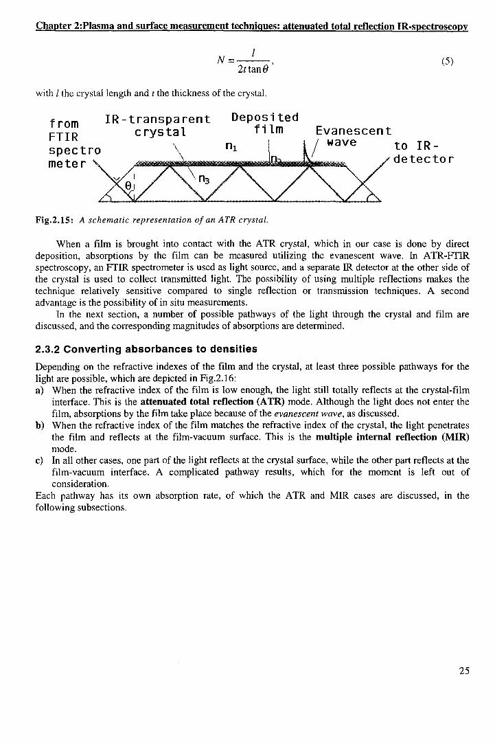
Chapter 2:Plasma and surface measurement technigues: attenuated total reflection IR-spectroscopy
N= l 2ttan8'
with l the crystallength and t the thickness of the crystal.
from FTIR
IR-transparent c rystal
Deposited film
(5)
Evanescent J wave to IR-
~--~._._._.__. .. ~ .. ~~'.-~ detector
Fig.2.15: A schematic representation of an ATR crystal.
When a film is brought into contact with the ATR crystal, which in our case is done by direct deposition, absorptions by the film can be measured utilizing the evanescent wave. In ATR-FTIR spectroscopy, an FfiR spectrometer is used as light source, and a separate IR detector at the other side of the crystal is used to collect transmitted light. The possibility of using multiple reflections makes the technique relatively sensitive compared to single reflection or transmission techniques. A secoud advantage is the possibility of in situ measurements.
In the next section, a number of possible pathways of the light through the crystal and film are discussed, and the conesponding magnitudes of absorptions are determined.
2.3.2 Converting absorbsnees to densities
Depending on the refractive indexes of the film and the crystal, at least three possible pathways for the light are possible, which are depicted in Fig.2.16: a) When the refractive index of the film is low enough, the light still totally reflects at the crystal-film
interface. Th is is the attenuated total reflection (A TR) mode. Although the light does not enter the film, absorptions by the film take place because of the evanescent wave, as discussed.
b) When the refractive index of the film matches the refractive index of the crystal, the light penetrates the film and reflects at the film-vacuum surface. This is the multiple internal reflection (MIR) mode.
c) In all other cases, one part of the light reflects at the crystal surface, while the other part reflects at the film-vacuum interface. A complicated pathway results, which for the moment is left out of consideration.
Each pathway bas its own absorption rate, of which the A TR and MIR cases are discussed, in the following subsections.
25
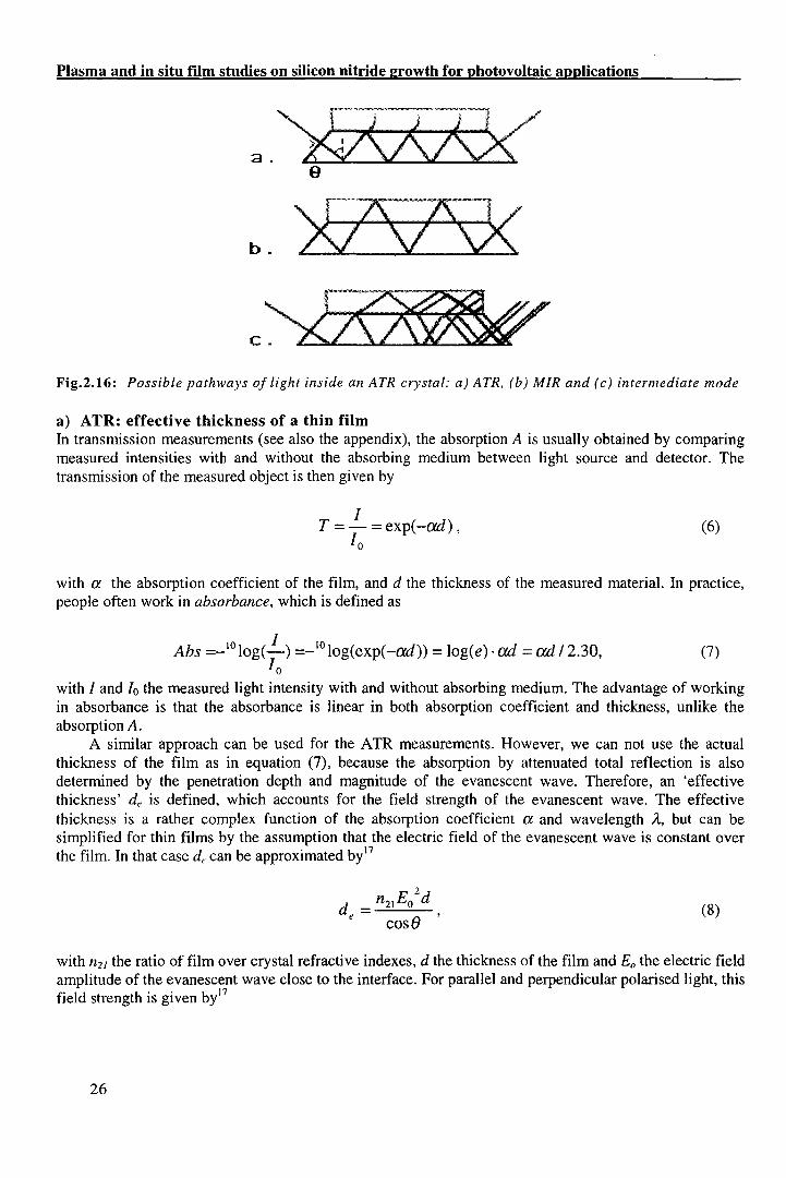
Plasma and in situ film studies on silicon nitride growth for photovoltaic applications
a.
b.
Fig.2.16: Possible pathways of light inside an ATR crystal: a) ATR, (b) MIR and (c) intermediatemode
a) ATR: effective thickness of a thin film In transmission measurements (see also the appendix), the absorption A is usually obtained by camparing measured intensities with and without the absorbing medium between light souree and detector. The transmission of the measured object is then given by
I T =I= exp(-ad),
0
(6)
with a the absorption coefficient of the film, and d the thickness of the measured materiaL In practice, people often work in absorbance, which is defined as
I Abs =-10 log(-) =-10 log(exp(-ad)) = log(e) ·ad= ad I 2.30, (7)
Io with I and /0 the measured light intensity withand without absorbing medium. The advantage of working in absorbance is that the absorbance is linear in both absorption coefficient and thickness, unlike the absorption A.
A similar approach can he used for the ATR measurements. However, we can not use the actual thickness of the film as in equation (7), because the absorption by attenuated total reflection is also determined by the penetration depth and magnitude of the evanescent wave. Therefore, an 'effective thickness' de is defined, which accounts for the field strength of the evanescent wave. The effective thickness is a rather complex function of the absorption coefficient a and wavelength À, but can be simplified for thin films by the assumption that the electric field of the evanescent wave is constant over the film. In that case de can be approximated by 17
2 d = n21Eo d
e cose ' (8)
with n21 the ratio of film over crystal refractive indexes, d the thickness of the film and Eo the electric field amplitude of the evanescent wave close to the interface. For parallel and perpendicular polarised light, this field strength is given by17
26
Chapter 2:Plasma and surface measurement technigues: attenuated total reileetion IR-spectroscopy
E = 2cos8 , and E11
= 2cos8
j_ ~1- n31 2 ~1- n31 2
(1 + n3/)sin 2 e -n312
2 . ? 2 , (1+n31 )sm-8-n31
(9)
with n32 the ratio of vacuum over film refractive indexes, n.u the ratio of vacuum over crystal refractive indexes and 0 the angle of incidence. Combining (8) and (9) gives the effective thickness de for parallel and perpendicular polarized light 17
:
del__ 4n21 cos8 de 11 _ 4n21 cos8((1+n324
)sin28-n31
2J -- - 2 , and -- - 2 2 . z 2 . d (1- n31 ) d (1- n31 ) (1 + n31 )sm e- n31
(10)
When the film is thin, 27td<À/10 (i.e. d<160 nm for lOJ.!m light), and the absorption coefficient is small, a<1.25n/À (i.e. a<6·104m·1 for lOJ.!m light in a film with refractive index of 2.1), these relations are correct within a few percent. For too high absorbances, the effective thickness is overestimated by equation ( 1 0), and hence the calculated density underestimated. The effective thickness may be greater or smaller than the actual film thickness by a large factor, and decreases with increasing angle of incidence. Also, the effective thickness for parallel polarization may be greater or smaller than that for perpendicular polarization, depending on whether n3/ln3/ is greater or smaller than I*. In the next section, examples of effective thicknesses for two used crystal types (made of Si and ZnSe) are given.
To summarize, the ATR absorptions can be treated analogously to transmission absorptions, by using the effective thickness de instead of d, as explained above. For an ATR crystal with N intemal reflections, we could write for the absorbance of a thin film, analogously to equation (7):
I Abs =-10 log(-) = Nade 12.30. (ll)
Io In practice, absorption peaks are integrated over their width. The bond density is calculated using the re lation
nbond = K f a dm' (1)
(12)
with Ka proportionality constant (reciprocal absorption cross section). Combining equation (11) and (12), the bond density is obtained from absorbances measured with an ATR crystal by
_ 2.30·KsAbsd nbond - -- (1).
Nde (1)
(13)
b) Multiple intern al reflection In case of matching refractive indexes, the light will enter the film undeflected and reflect at the filmvacuum surface. The film absorption A of the light in MIR mode during each reflection is then determined by the light pathlength in the film l=2dlcos and absorption coefficient a. Hence, we can write for the absorbance
Abs = a(2djcos8) /2.30, (14)
• Por the used crystals Si and ZnSe, the perpendicular field strengths are respectively 0.96 and 1.06 times as large as the parallel field when measuring films with a refractive index of 2.1.
27
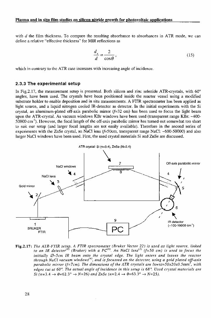
Plasma and in situ film studies on silicon nitride growth for photovoltaic applications
with d the film thickness. To campare the resulting absorbance to absorbances in A TR mode, we can define a relative "effective thickness" for MIR reflections as
de 2 d cose'
(15)
which in contrary to the ATR case increases with increasing angle of incidence.
2.3.3 The experimental setup
In Fig.2.17, the measurement setup is presented. Bath silicon and zinc selenide ATR-crystals, with 60° angles, have been used. The crystals have been positioned inside the reactor vessel using a modified substrate holder to enable deposition and in situ measurements. A FTIR spectrometer has been applied as light source, and a liquid nitrogen caoled IR-detector as detector. In the initial experiments with the Si crystal, an aluminum-plated off-axis parabalie mirror if=32 cm) has been used to focus the light beam upon the ATR-crystal. As vacuum windows KBr windowshave been used (transparent range KBr: -400-50000 cm-1
). However, the focallength of the off-axis parabalie mirror has turned out somewhat too short to suit our setup (and larger focal lengtbs are not easily available). Therefore in the second series of experiments with the ZnSe crystal, an NaCl lens if=50cm, transparent range NaCl: -600-50000) and also larger NaCl windows have been used. First, the used crystal materials Si and ZnSe are discussed.
ATR crystal: Si (n=3.4), ZnSe (N=2.4)
\ 7
NaCI windows
NaCIIens ~4
~ 3 ~\,~---Gold mirror ~ ·
\2~
1 BRUKER
FTIR
9
PC
I
Off-axis parabalie mirror
6
IR detector (-100-10000 cm·1
)
Fig.2.17: The ATR-FTIR setu;r. A FTIR sp~ctromete; (Bruker Vector p) is used as_ light source, linked to an IR detector1 (Bruker) wlth a PC1 1. An NaCl lensr. 1 (f=50 cm) ts used to focus the initially 0-5cm IR beam onto the crystal edge. The light enters and leaves the reactor through Na Cl vacuum windowsf41, and is focussed on the detector, using a gold plated off-axis parabalie mirror (f=7cm). The dimensions of the ATR crystals are lxwxt=50x20x0.5mm3
, with edges cut at 60°. The actual angle of incidence in this setup is 68°. Used crystal materials are Si (n=3.4 -4 8=62.3° -4 N=26) and ZnSe (n=2.4 -4 8=63.3° -4 N=25).
28
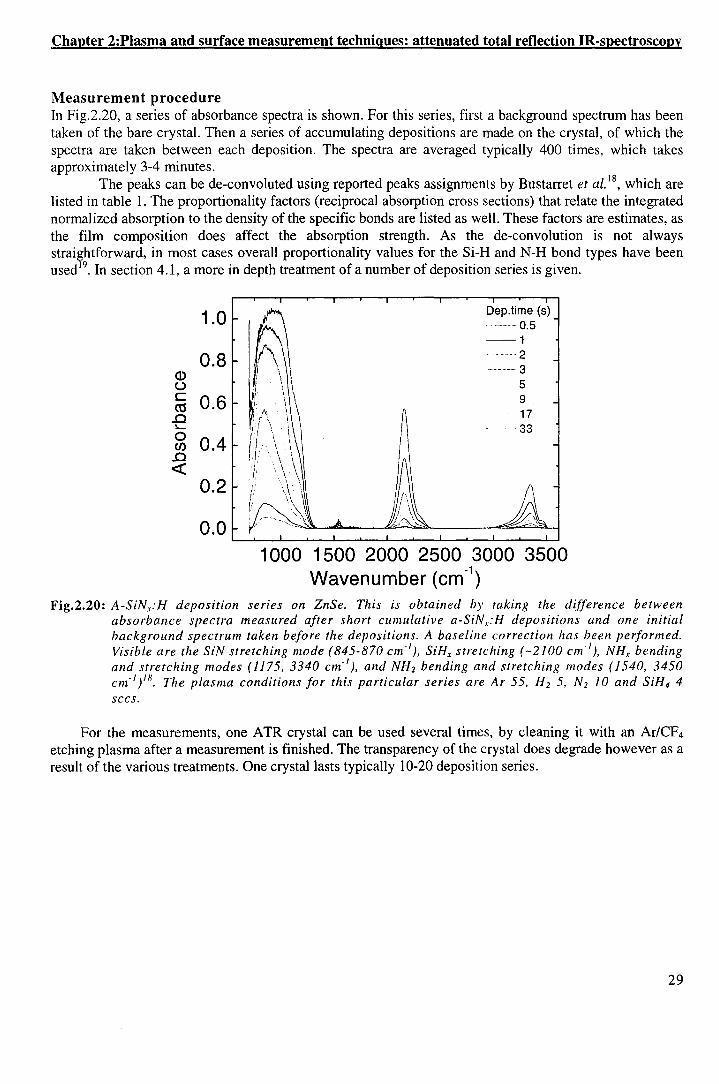
Chapter 2:Plasma and surface measurement technigues: attenuated total reileetion IR-spectroscopy
Measurement procedure In Fig.2.20, a series of absorbance spectra is shown. For this series, first a background spectrum has been taken of the bare crystal. Then a series of accuroulating depositions are made on the crystal, of which the spectra are taken between each deposition. The spectra are averaged typically 400 times, which takes approximately 3-4 minutes.
The peaks can be de-convoluted using reported peaks assignments by Bustarret et al. 18, which are
Iisted in table 1. The proportionality factors (reciprocal absorption cross sections) that relate the integrated normalized absorption to the density of the specific bands are listed as well. These factors are estimates, as the film composition does affect the absorption strength. As the de-convolution is not always straightforward, in most cases overall proportionality values for the Si-H and N-H bond types have been used 19
• In section 4.1, a more in depth treatment of a number of deposition series is given.
1.0
0.8 Q) (.) c 0.6 ct! ..c
I....
0 0.4 (/) ..c <(
0.2
0.0
Dep.time (s) 0.5
--1 2
...... 3
5 ............ 9
--17 -- 33
1000 1500 2000 2500 3000 3500 Wavenumber (cm-1
)
Fig.2.20: A-SiN_,."H deposition series on ZnSe. This is obtained hy taking the difference between abs01·bance spectra measured aft er short cumulative a-SiN,: H depositions and one initia/ background spectrum taken befare the depositions. A baseline correction has been performed. Visible are the SiN stretching mode (845-870 cm- 1
), SiHx stretching (-2100 cm- 1), NHx bending
and stretching modes ( 1175, 3340 cm· 1 ), and NH2 bending and stretching modes (1540, 3450
cm· 1 )
111• The plasma conditions for this particular series are Ar 55, H2 5, N2 JO and SiH4 4
sccs.
For the measurements, one ATR crystal can be used several times, by cleaning it with an Ar/CF4 etching plasmaaftera measurement is finished. The transparency of the crystal does degrade however as a result of the various treatments. One crystallasts typically 10-20 deposition series.
29
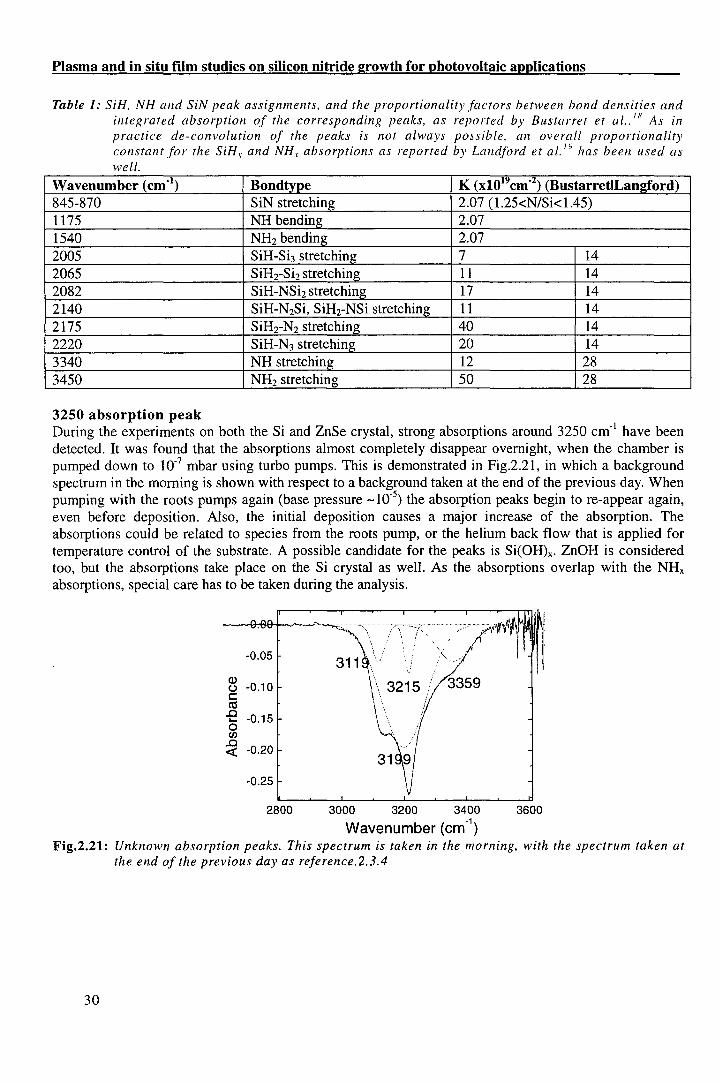
Plasma and in situ film studies on silicon nitride growth for photovoltaic applications
Table 1: SiH, NH and SiN peak assignments, and the proportionality factors between bond densities and integrated absorption of the con·esponding peaks, as reported by Bustarret et al .. 18 As in practice de-convolution of the peaks is not always possible, an overall proportionality constant for the SiHx and NHx absorptions as reported by Landford et al. 1 ~ has been used as wel!.
Wavenumber (cm"1) Bondtype K (x1019cm-2
) (BustarretiLangford) 845-870 SiN stretching 2.07 (1.25<N/Si<1.45) 1175 NH bending 2.07 1540 NH2 bending 2.07 2005 SiH-Sb stretching 7 14 2065 SiH2-Si2 stretching 11 14 2082 SiH-NSh stretching 17 14 2140 SiH-N2Si, SiH2-NSi stretching 11 14 2175 SiH2-N2 stretching 40 14 2220 SiH-N3 stretching 20 14 3340 NH stretching 12 28 3450 NH2 stretching 50 28
3250 absorption peak During the experiments on both the Si and ZnSe crystal, strong absorptions around 3250 cm·1 have been detected. It was found that the absorptions almost completely disappear ovemight, when the chamber is pumped down to 10-7 mbar using turbo pumps. This is demonstrated in Fig.2.21, in which a background spectrum in the moming is shown with respect to a background taken at the end of the previous day. When pumping with the roots pumps again (base pressure -10-5
) the absorption peaks begin to re-appear again, even before deposition. Also, the initia} deposition causes a major increase of the absorption. The absorptions could be related to species from the roots pump, or the helium back flow that is applied for temperature control of the substrate. A possible candidate for the peaks is Si(OH)x- ZnOH is considered too, but the absorptions take place on the Si crystal as well. As the absorptions overlap with the NHx absorptions, special care has tobetaken during the analysis.
-0.05
·~· Q)
-0.10 (.) c m .0 -0.15 ,_ 0 (/)
.0 -0.20 <(
-0.25
2800 3000 3200 3400 3600
Wavenumber (cm.1)
Fig.2.21: Unknown absorption peaks. This spectrum is taken in the morning, with the spectrum taken at the end of the previous day as reference.2.3.4
30
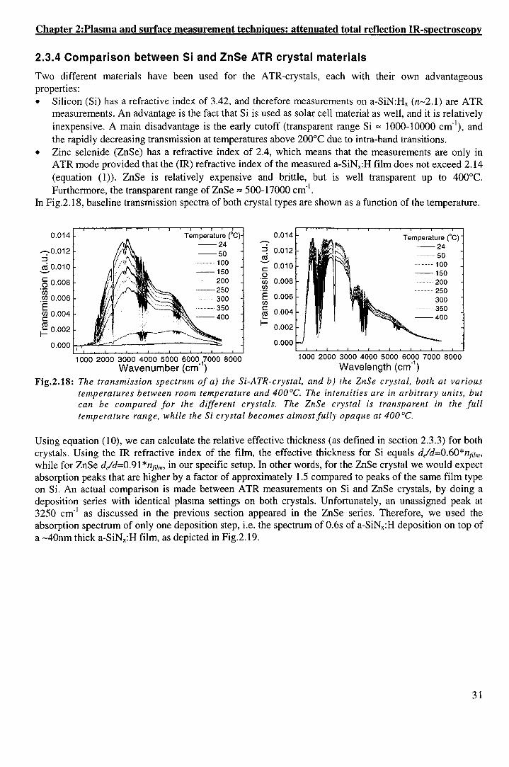
Chapter 2:Piasma and surface measurement technigues: attenuated total reflection IR-spectroscopy
2.3.4 Comparison between Si and ZnSe ATR crystal materials
Two different materials have been used for the ATR-crystals, each with their own advantageous properties: • Silicon (Si) has a refractive index of 3.42, and therefore measurements on a-SiN:Hx (n-2.1) are ATR
measurements. An advantage is the fact that Si is used as solar cell material as well, and it is relatively inexpensive. A main disadvantage is the early cutoff (transparent range Si"" 1000-10000 cm-1
), and the rapidly decreasing transmission at temperatures above 200°C due to intra-band transitions.
• Zinc selenide (ZnSe) has a refractive index of 2.4, which means that the measurements are only in ATR mode provided that the (IR) refractive index of the measured a-SiNx:H film does not exceed 2.14 (equation (1)). ZnSe is relatively expensive and brittle, but is well transparent up to 400°C. Furthermore, the transparent range of ZnSe "" 500-17000 cm·1
•
In Fig.2.18, baseline transmission spectra of both crystal types are shown as a function of the temperature.
0.014 Temperature --24
...--;-0.012 --50 ::I 100 ~0.010 --150
§ 0.008 200
ëi.i -----250 .!Q 0.006 300 E ·········-····- 350 ê 0.004 ctl ~ 0.002
0.000
1000 2000 3000 4000 5000 6000,7000 8000 Wavenumber (cm· )
0.014 -:::l 0.012 ~
0.010 c:: .Q
0.008 (/)
.!Q E 0.006 (/)
c:: 0.004 ctl .....
I- 0.002
0.000
Temperature ("C) --24 ----50
100 --150
200 ................ 250
300 .................... 350 --400
1000 2000 3000 4000 5000 6000 7000 8000 Wavelength (cm-1
)
Fig.2.18: The transmission spectrum of a) the Si-ATR-crystal, and b) the ZnSe crystal, bath at various temperafttres between room temperafure and 400°C. The intensities are in arbitrary units, but can be compared for the different crystals. The ZnSe crystal is transparent in the Juli temperafure range, while the Si crystal becomes almast fully opaque at 400 oe.
Using equation (1 0), we can calculate the relative effective thickness (as defined in section 2.3.3) for both crystals. Using the IR refractive index of the film, the effective thickness for Si equals d/d=0.60*nfi111"
while for ZnSe d/d=0.91 *nfi1n" in our specific setup. In other words, for the ZnSe crystal we would expect absorption peaks that are higher by a factor of approximately 1.5 compared to peaks of the same film type on Si. An actual comparison is made between ATR measurements on Si and ZnSe crystals, by doing a deposition series with identical plasma settings on bath crystals. Unfortunately, an unassigned peak at 3250 cm· 1 as discussed in the previous section appeared in the ZnSe series. Therefore, we used the absorption spectrum of only one deposition step, i.e. the spectrum of 0.6s of a-SiNx:H deposition on top of a -40nm thick a-SiNx:H film, as depicted in Fig.2.19.
31
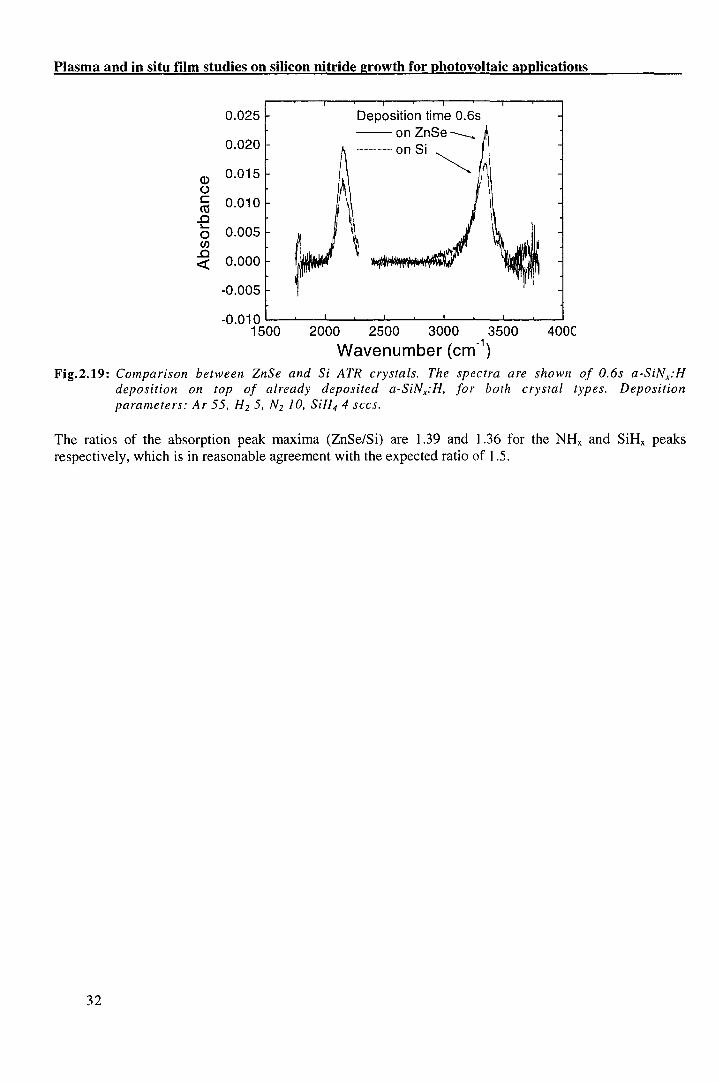
Plasma and in situ film studies on silicon nitride growth for photovoltaic applications
0.025
0.020
Q) 0.015 (.) c 0.010 Cl3 .0 ......
0.005 0 en .0
0.000 <(
-0.005
-0.010 1500
Deposition time 0.6s --on ZnSe--
................. on Si
~ f' \ \ I I
2000 2500 3000 3500 400(
Wavenumber (cm-1)
Fig.2.19: Comparison between ZnSe and Si ATR crystals. The spectra are shown of 0.6s a-SiNx:H deposition on top of already deposited a-SiNx:H, for bath crystal types. Deposition parameters: Ar 55, H2 5, N2 JO, SiH4 4 sccs.
The ratios of the absorption peak maxima (ZnSe/Si) are 1.39 and I .36 for the NHx and SiHx peaks respectively, which is in reasonable agreement with the expected ratio of 1.5.
32
Chapter 3: Plasma radical densities during a-SiN!:H deposition
Chapter 3
Plasma radical densities during a-SiNx:H deposition
In this chapter, the measurements performed on the a-SiNx:H depositing plasma are presented. The deposition reaction scheme as described in chapter 1, i.e. nitridation of an a-Si:H-Iike top layer, has been used as a starting point for the plasma measurements. This model suggests that a-Si:H depositing radicals tagether with 'nitridating' species, either atomie N radicals or possibly excited N2 molecules, bring about the deposition of a-SiNx:H. In this study, an attempt is made to find out which exact radicals establish the deposition. In section 3.1, first dissociation mechanisms of the SiH4 precursor are discussed, which play an important role in the a-Si:H depositing plasma and could occur in the a-SiNx:H depositing plasma as well. In section 3.2, measured densities of radicals in the non-depositing souree plasma that might be responsible for the dissociation of SiH4 are presented. In section 3.3, measured densities of N and SiH3 in the depositing plasma are shown. Also the SiH density has been measured. In section 3.4 the plasma densities are discussed in correlation to film composition and growth rate as measured by ERD and ellipsometry. It is verified whether the measured N and SiH3 densities are high enough to explain the deposition rate. Finally, insection 3.5 some other observations in the plasma are presented.
3.1 Precursor dissociation mechanisms As discussed in chapter 1, the dissociation of SiH4 takes place in a low pressure deposition chamber, by means of an Ar/H2/N2 plasma that is generated in a high-pressure cascaded are plasma source. We will first consider which of the species that are emanating from the plasma souree could dissociate SiH4. Previous Langmuir probe measurements on the plasma have pointed out that the electron temperature in this plasma is relatively low at 0.3-0.4 eV, which means that electroos most likely do not play a major role in the precursor dissociation reactions. Furthermore, it is shown that the ion density decreases from -1019m-3 (mainly Ar+) to -1017m-3 (mainly NH/) when hydragen and nitrogen are admixed to the plasma23
•
From previous studies on the a-Si:H depositing plasma, both ions and atomie H are known to provide reaction pathways that lead to the dissociation of SiH4. Ar+ can dissociate SiH4 by dissociative charge exchange in the reaction5
:
(1)
which is a relatively efficient reaction. Subsequent dissociative recombination reactions of SiH/ with electrans lead to the production of SiHn (n:Q) radicals, which are very reactive, both in the plasma with SiH4 and on the surface. As mentioned, the ion density is however low in the Ar/H2/Nz plasma when H2 is added to the plasma. In that case (just as in the case of a-Si:H deposition) the following reaction5 is thought to become predominant:
(2)
Subsequent H-abstraction reactions of the SiHx radicals with H may occur, but as long as there is no abundance of H, the SiH3 radical is expected to be produced in much higher density than the SiHn (n::;;2) radicals.
Because of the Jack of Si-N containing species in an Ar/N2/SiH4 RF plasma as reported by Srnith et af. 1
•2
, atomie N is not expected to be very reactive with SiH4 in the plasma phase, but dissociation reactions of SiH4 invalving N can still be possible. Therefore we have measured the densities of both H and N in the souree plasma, as presented in the following section.
33
Plasma and in situ film studies on silicon nitride growth for photovoltaic applications
3.2 N and H radical densities from the Ar/N:z/H2 plasma souree
(without SiH4 injection)
Density Ç without--
2.5 .........
H2
flow
• • T
'i' E 2.0
"' ~0 1.5 T"""
>--1.0 ·c;; c • Q)
+ "0 0.5 z ••
0.0 • 0 2 4 6 8 10
N2
flow (sccs) Fig.3.1: Atomie N density in a Ar!N21Hrplasma [Ar 55, H 2 5, N2 0-10 sccs, 45A], as a function of the N2
flow, as measured with TJMS.
In Fig.3.1, the N density in the Ar/H2/N2 souree plasma is shown as a function of the N2 flow. The density has been measured using TIMS (chapter 2.2), at the position of the substrate holder. The N density increases with increasing N2 flow to 1-2·1 019 m·3
, i.e. the production of Nis not limited by the capacity of the plasma source. The order of magnitude of the absolute density is in agreement with T ALIF measurements, where a density of 5'1019 m·3 was determined duringa pure 25 sccs N2 plasma at a pressure of 0.20 mbar25
. As shown in the same figure, the addition of H2 reduces the N density by approximately 50%.
Unfortunately, atomie H is generally more difficult to measure. We have been able to detect atomie H using the TIMS technique, but the relative error due to time-dependent artifacts in these results is too high to present the H density series. However, the measurements suggest an absolute density in the range of 2·1018-7-1019 m3.*
The main condusion is that the measurements suggest that both neutral N and H are present in high enough density in the souree plasma for the majority of precursor dissociation reactions in the depositing plasma. In the next section N and SiHx radical density measurements in the depositing plasma (i.e. with SiH4) will be presented.
3.3 N, SiH3 and SiH radical densities in the Ar/H~JSiH4 depositing plasma In Fig.3.2, the measured N density is shown, but now with SiH4 being added to the downstream
plasma, using the injection ring. Interestingly, the SiH4 addition leads initially to a steep increase of the N density by a factor of 5-6, to a very high density of -1020m·3
. Th is is foliowed by a gradual decrease with increasing SiH4 flow. The remarkably sharp initia! increase in N density is not expected and not understood yet. In fact, the possibility of reactions of atomie N with SiHx in the plasmaand at the surface would more likely result in a lower density, because moreN atoms are consumed per unit of time. If we reverse this reasoning, the fact that SiH4 addition leads to an increase in N density supports the idea that atomie N is indeed not very reactive with SiHx. It should be noted however, that TIMS is a local measurement technique (unlike e.g. CRDS, where the density is integrated over the line of sight through the plasma). Therefore, apart from new reaction mechanisms, a possible explanation for the jump could be
* Depending on the proportionality factor C for the background density inside the mass spectrometer, which depends on the wall recombination probability of atomie H, as discussed in chapter 2.2.
34
Chapter 3: Plasma radical densities durlog a-SiN!:H deposition
a confinement of the plasma due to the silane injection, i.e. N atoms might have a lower diffusivity to the wall upon SiH4 addition. An increased density by a factor of 5 would correspond with a decreased
"diameter of the plasma" by a factor of .J5 . Such a confinement can not be seen in the CROS measurements without making a radial scan of the density. Another possibility to be considered is the availability of SiHx related reaction pathways leading to dissociation of (excited) N2, although such reactions would require a lot of energy as the N2 bond is a relatively strong bond. A third possible explanation is a decreased consumption of N in reactions with H, because of H being consumed in the precursor dissociation reactions (reaction 2).
The subsequent gradual decrease of the N density can be explained by an increased consumption of N on the surface, due to a higher incorporation rate of N in the a-SiNx:H film that is being grown with increasing growth rate as the SiH4 flow is increased. This will be verified with ERD datainsection 3.4.
14
• - 12 "? E
0> 10 ~
0 ~
8 .._ >-
:!::::: en 6 c:
• • t •
• •
Q) "0 4 z
2 • 0
0 2 4 6 8 10 12 SiH
4 flow (sccs)
Fig.3.2: Atomie N density in an Ar/N2/H2/SiHrplasma [Ar: SS, H2:5, N2: JO, SiH4:0-12 sccs], as measured with TIMS.
CROS density measurements of SiH3, the other expected main radical, and SiH are shown in Figs.3(a) and (b). A density of 1-2·1019m·3 is measured for the 'standard' a-SiNx:H deposition conditions with 8 sccs SiH4. The addition of N2 to the plasma leads to a density which is about twice as high as same condition without N2. This could indicate that N is involved in dissociation reactions with SiH4, but the increased density may as well be explained by a higher reactivity of the plasma due to a higher power u sage of the are. The are plasma souree is current controlled, not power controlled, and at higher gas flows usually a higher voltage (and hence more power) is needed to maintain the same current through the plasma. This explanation could apply for the increased SiH density upon N2 addition as well.
35
Plasma and in situ film studies on silicon nitride growth for photovoltaic applications
lU 10
-- '? '?
+ + E E ~
~
+ 0
0 ..-
t x ..- -.è' +
>.
+ ;'.:;:! • (/)
+ (/) • • c c • Q) 0 Q)
"C "C M
I I • density I ü5 density (/) D-without
without N2
flow N
2 flow Hoefnagels
0.1 1 10 10
SiH4
flow (sccs) SiH4-flow (sccs)
Fig.3.3: SiH3 (a) and SiH (b) density in an Ar/H2/N2/SiHrplasma vs. SiH4 flow [Ar 55, H 2 5, N2 JO, SiH4 0-15 sccs], as measured using CRDS.
As visible from Fig.3.3, the SiH3 density is about two orders higher compared to the SiH density. This large difference between both densities indicates that the proposed reaction scheme (2), in which SiH3 is created by H abstraction reaction from SiH4, is dominant over reaction (1 ), as expected. The flattening-off trend of SiH may be explained by a competition of SiH creation (either by reaction (1) or reaction (2)), and loss in reactions of SiH with SiH,.
The fact that both SiH3 and N radicals are present in high densities supports (at least does not contradict) the proposed deposition model of nitridation of an a-Si:H-Iike layer (section 1.3). In the next section, a quantification is done of the contribution of the SiH3 and N radicals to the film growth, by comparing the radical densities in the plasma to the growth rate and composition of the films.
3.4 Contribution of SiH3, SiH and N radicals to the film growth In Fig.3.4a, the a-SiNx:H film growth rateis shown as a function of the SiH4 flow, at a constant N2
flow of 10 sccs. In Fig.3.4b, the N/Si ratio in the deposited films deposited under the same plasma conditions is shown. As the growth rate increases nearly linearly with the SiH4 flow, the film composition changes from a N-rich film to Si-rich film. At very low SiH4 flows, the films become nearly stochiometric ShN4: it is not possible to produce films with much higher N/Si ratios than 1.33. Evidently, the change from N-rich to Si-rich films must be caused by the changed ratio of N and SiH, radicals present in the plasma. In this section, it is investigated to what extent the measured N and SiH3 densities in the plasma can explain the film composition and growth rate.
36
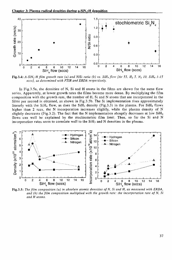
Chapter 3: Plasma radical densities during a-SiN:éH deposition
40 1.5
• ! ! stochiometric Si
3N
4 -(/) 1.2 ! ..._ 30 E c 0 - 0.9 (])
:;::::; ces ....... ....
~ 20 • i:i5 ..c ....... 0.6 ....... z :s: • 0 10 .... 0.3 ~ • •
0 0.0 0 2 4 6 8 10 12 14 16 0 2 4 6 8 10 12 14 16
SiH4
flow (sccs) SiH4
flow (sccs)
Fig.3.4: A-SiNx:H film growth rate (a) and N!Si ratio (b) vs. SiH4 flow [Ar 55, H2 5, N 2 JO, SiH4 1-15 sccs], as determined with FTIR and ERDA respectively.
In Fig.3.5a, the densities of N, Si and H atoms in the films are shown for the same flow series. Apparently, at lower growth rates the films become more dense. By multiplying the film composition with the growth rate, the number of H, Si and N atoms that are incorporated in the films per second is obtained, as shown in Fig.3.5b. The Si implementation rises approximately linearly with the SiH4 flow, as does the SiH3 density (Fig.3.3) in the plasma. For SiH4 flows higher than 2 sccs, the N incorporation increases slightly, while the plasma density of N slightly decreases (Fig.3.2). The fact that the N implementation abruptly decreases at low SiH4 flows can well be explained by the stochiometric film limit. Thus, so far the Si and N incorporation rates seem to correlate well to the SiH3 and N densities in the plasma.
- 7 <')
E (.)
6 -(/) E 5 0 ....... ces
C\1 4 C\1 0 T"" 3 x ->- 2 ."t:: (/)
c (])
0 0
0
'• ik/ \ '·. ' \ · . I \ ·.
-- Hydragen --e-Silicon
A ··· Nitrogen . \
\' --· \\ --'!:;; ..... -------·---·-------
2 4 6 8 10 12 14 16 SiH
4 flow (sccs)
-(/)
C\IE 14 (.)
~ 12 ces "'
-- Hydragen •-- Silicon A Nitrogen
/
/ /
/
/
0 2 4 6 8 10 12 14 SiH
4 flow (sccs)
16
Fig.3.5: The film composition (a) in absolute atomie densities of N, Si and H, as measured with ERDA, and (b) the film composition multiplied with the growth rate: the incorporation rate of N, Si and H atoms.
37
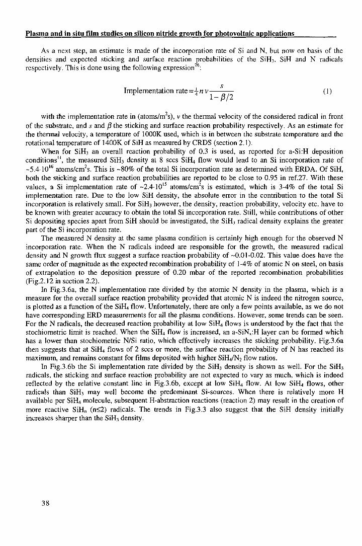
Plasma and in situ film studies on silicon nitride growth for photovoltaic applications
As a next step, an estimate is made of the incorporation rate of Si and N, but now on basis of the densities and expected sticking and surface reaction probabilities of the SiH3, SiH and N radicals respectively. This is done using the following expression26
:
Implementation rate=tn v s 1- {3 /2
(1)
with the implementation rate in (atoms/m2s), v the thermal velocity of the considered radical in front of the suhsrrate, and s and f3 the sticking and surface reaction probability respectively. As an estimate for the thermal velocity, a temperature of 1000K used, which is in between the substrate temperature and the rotationai temperature of 1400K of SiH as measured by CRDS (section 2.1).
When for SiH3 an overall reaction probability of 0.3 is used, as reported for a-Si:H deposition conditions i 1, the measured SiH3 density at 8 sccs SiH4 flow would lead to an Si incorporation rate of -5.4·1016 .atoms/cm2s. This is -80% of the total Si incorporation rate as determined with ERDA. Of SiH, both the sticking and surface reaction probabilities are reported to be close to 0.95 in ref.27. With these values, a Si implementation rate of -2.4·1015 atoms/cm2s is estimated, which is 3-4% of the total Si implementation rate. Due to the low SiH density, the absolute error in the contribution to the total Si incorporation is relatively small. For SiH3 however, the density, reaction probability, velocity etc. have to be known with greater accuracy to obtain the total Si incorporation rate. Still, while contributions of other Si depositîng species apart from SiH should be investigated, the SiH3 radical density explains the greater part of the Si incorporation rate.
The measured N density at the same plasma condition is certainly high enough for the observed N incorpomtion rate. When the N radicals indeed are responsible for the growth, the measured radical density and N growth flux suggest a surface reaction probability of -0.01-0.02. This value does have the same order of magnitude as the expected recombination probability of 1-4% of atomie N on steel, on basis of extrapolation to the deposition pressure of 0.20 mbar of the reported recombination probabilities (Fig.2.12 .in section 2.2).
In Fig.3.6a, the N implementation rate divided by the atomie N density in the plasma, which is a measure for the overall surface reaction probability provided that atomie N is indeed the nitrogen source, is plottedas a function of the SiH4 flow. Unfortunately, there are only a few points available, as we do not have corresponding ERD measurements for all the plasma conditions. However, some trends can be seen. For the N radicals, the decreased reaction probability at low SiH4 flows is understood by the fact that the stochiometric limit is reached. When the SiH4 flow is increased, an a-SiNx:H layer can be formed which bas a lower than stochiometric N/Si ratio, which effectively increases the sticking probability. Fig.3.6a then suggests that at SiH4 flows of 2 sccs or more, the surface reaction probability of N has reached its maximum, and remains constant for films deposited with higher SiHJN2 flow ratios.
In Fig.3.6b the Si implementation rate divided by the SiH3 density is shown as wel!. For the SiH3
radicals, the sticking and surface reaction probability are not expected to vary as much, which is indeed reflected by the relative constant line in Fig.3.6b, except at low SiH4 flow. At low SiH4 flows, other radicals than SiH3 may well become the predominant Si-sources. When there is relatively more H available per SiH4 molecule, subsequent H-abstraction reactions (reaction 2) may result in the creation of more reactive SiHn (n~2) radicals. The trends in Fig.3.3 also suggest that the SiH density initially increases sharper than the SiH3 density.
38
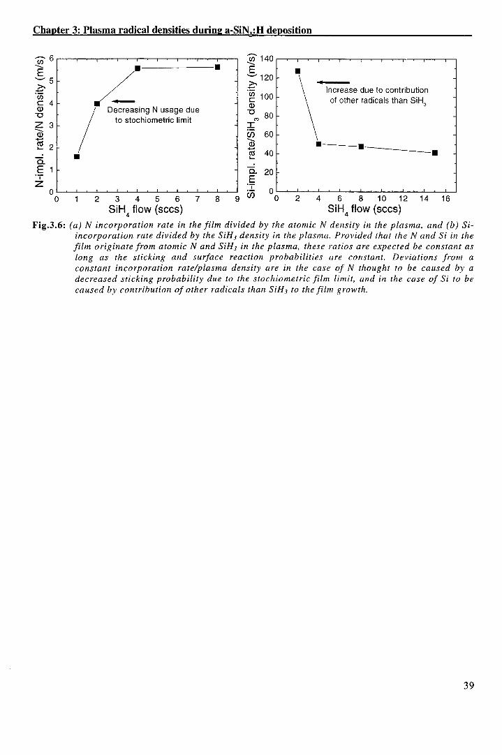
Chapter 3: Plasma radical densities during a-SiN.3:H deposition
(j)6r-~,---,.---,,---,.---,,---,----,----r----,~---.~--.-~-,---.--, i: /-·-------· ~ I Oecreasing N usage due
to stochiometric limit z 3 -Q) ..... ~ 2
0.. •
E I z
0.. 20 E .,
0o~~~~2~~3~~4~~5~~6~~7~~8~~9 00 SiH
4 flow (sccs)
•
2
lncrease due to contribution of other radicals than SiH
3
·---· ------•
4 6 8 10 12 14 16 SiH
4 flow (sccs)
Fig.3.6: (a) N incorporation rate in the film divided by the atomie N density in the plasma, and (b) Siincorporation rate divided by the SiH3 density in the plasma. Provided that the N and Si in the film originate from atomie N and SiH3 in the plasma, these ratios are expected be constant as long as the sticking and surface reaction probabilities are constant. Deviations from a constant incorporation ratelplasma density are in the case of N thought to be caused by a decreased sticking probability due to the stochiometric film limit, and in the case of Si to be caused by contribution of other radicals than SiH3 to the film growth.
39
Chapter 4: In situ film study
Chapter 4
In situ film study
In this chapter the in situ a-SiNx:H film studies performed with the ATR-FTIR technique, as introduced in chapter 2.3, are presented. With this technique, the infrared absorptions by Si-H, N-H and S-N honds have been monitored in a number of experiments. In sections 4.1, three measured deposition series are discussed, which have been deposited with a varied SiHJN2 flow ratio. In section 4.2, the variation in depth of the a-SiNx:H films is discussed. In section 4.3, a study in which the growth mechanism is investigated more closely is described.
4.1 N-rich- Si-rich a-SiNx:H films In Fig.4.1, IR absorbance spectra that are made during three a-SiNx:H deposition series are
depicted. The films have been deposited on a ZnSe ATR crystal. Three plasma conditions with a high, medium and low N2/SiH4 flow ratio were used, by maintaining an N2 flow of 10 sccs and using 1, 4 and 8 sccs SiH4 respectively. The resulting films have a NISi-content that varies from nearly N-rich to Sirich. The spectra are measured aftera number of short cumulative depositions, each time interrupted for the measurement. One measurement takes approximately 5 minutes.
In the spectra, respective absorption peaks of SiN stretching (700-1000 cm-1), NH bending (1175
cm·\ NH2 bending (1540 cm-1) and SiHx (2005-2175 cm·\ NH (3340 cm-1
) and NH2 (3450 cm-1)
stretching modes are visible, as indicated in the middle graph. Also, some oxygen related absorption peaks are present of SiO (1050 cm·\ possibly SiOH (broad around 3250 cm·\ as wellas an absorption around 2264 cm·1 which is thought to be caused by SiHx with an oxygen environment. First we will consider the differences between the film types, by comparing the spectra of films with an approximately equal thickness of -40 nm.
In Fig.4.2, the SiN stretching + NH bending, SiHx and NHx stretching peaks are singled out, shown from left to right. From top to bottom, the three film types ranging from nearly N-rich to Si-rich are organized. As visible, with decreasing SiH4 flow, the absorption by SiHx decreases relative to the NHx absorption. The trend of NHx and SiHx roughly follows the N/Si ratio (Fig.3.3) in the film, but at I sccs SiH4, practically all the hydrogen that is present in the film is bonded to N. Furthermore, the SiHx absorption peak shows a shift to higher wavenumbers when relatively more N is present in the films. This is due to the generally observed fact that absorptions by Si-H bonds shift to higher wavenumbers when the electronegativity of the back-bonded atoms to Si is increased. N has a higher electronegativity than Si.
With decreasing SiHJN2 flow ratio (resulting in more N-rich films), an increasing SiO peak around I 050 cm·1 appears. Also a number of yet unassigned, possibly 0-related absorptions at 2264, 3170 and 3250 cm-1 are present. The increasing 0 content with decreasing SiH4 flow can be explained by the lower growth rate. A lower growth rate while having a constant pressure of oxygen in the chamber would result in relatively more oxygen incorporated in the film. Another explanation is found in a more porous structure of the films due to a higher relative N density in the plasma.
41
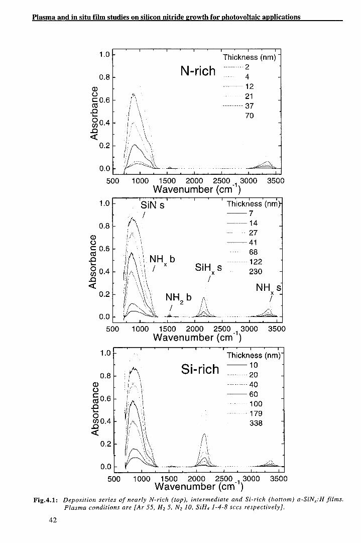
Plasma and in situ film studies on silicon nitride growth for photovoltaic applications
1.0
0.8 Q) (.)
C0.6 ctS ..c l....
~0.4 ..c <(
0.2
0.0
;\\
l \ i \
( \ f \ i \
N-rich Thickness (nm) ------- 2
4 --12
21 ................ 37
70
~~~~~~--~~--~~--~~--~~
Q) (.)
500
1.0
0.8
c 0.6 ctS ..c
l....
~ 0.4 ..c <(
0.2
0.0
1000 1500 2000 2500 1 3000 3500 Wavenumber (cm-)
SiN s Thickness (nm I --7
(• .... \\., ' ---- 14 /( 1 27 i:"'\ --41 r \ ! 68
NH b I x
SiH s ........................... 122 x 230
I NH s
x I
500 1 000 1500 2000 2500 -1 3000 3500 Wavenumber (cm )
1.0
0.8 Q) (.) c ctS 0.6 ..c
l....
0 U>0.4 ..c <(
0.2
0.0
/'\ i \ I \ i \ 1'. . !i \1 i
\ !
; !
Si-rich
{\ / \ { I i I
,_ )0\ . .... . ·~-. .q._-·.·~· ~
Thickness (nm) --10
.... 20
40 --60
100 ... 179
338
·'' g'"~---
500 1 000 1500 2000 2500 1 3000 3500 Wavenumber (cm- )
Fig.4.1: Deposition series of nearly N-rich (top), intermediate and Si-rich (bottom) a-SiNx:H films. Plasma conditions are [Ar 55, H2 5, N2 JO, SiH4 1-4-8 sccs respectively].
42
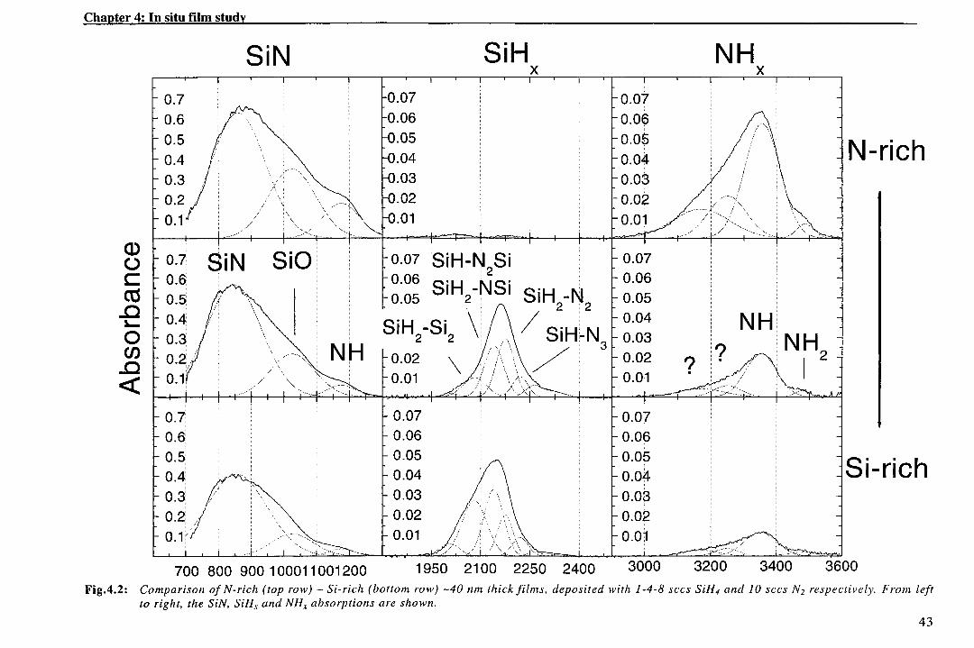
Chapter 4: In situ film study
Q) (.) c ct1 .c ~
0 en .c <(
0.7 0.6
~:~ Á 0.3;· 0.2 .'
0.1
SiN
700 800 900100011001200
0.07 0.06 0.05 0.04 0.03 0.02 0.01
SiH x
1950 2100 2250 2400 3000
NH x
N-rich
Si-rich
3200 3400 3600 Fig.4.2: Comparison of N-rich (top row)- Si-rich (bottom row) -40 nm thickfilms, deposited with 1-4-8 sccs SiH4 and JO sccs N2 respectively. From left
to right, the SiN, SiHx and NHx absorptions are shown.
43
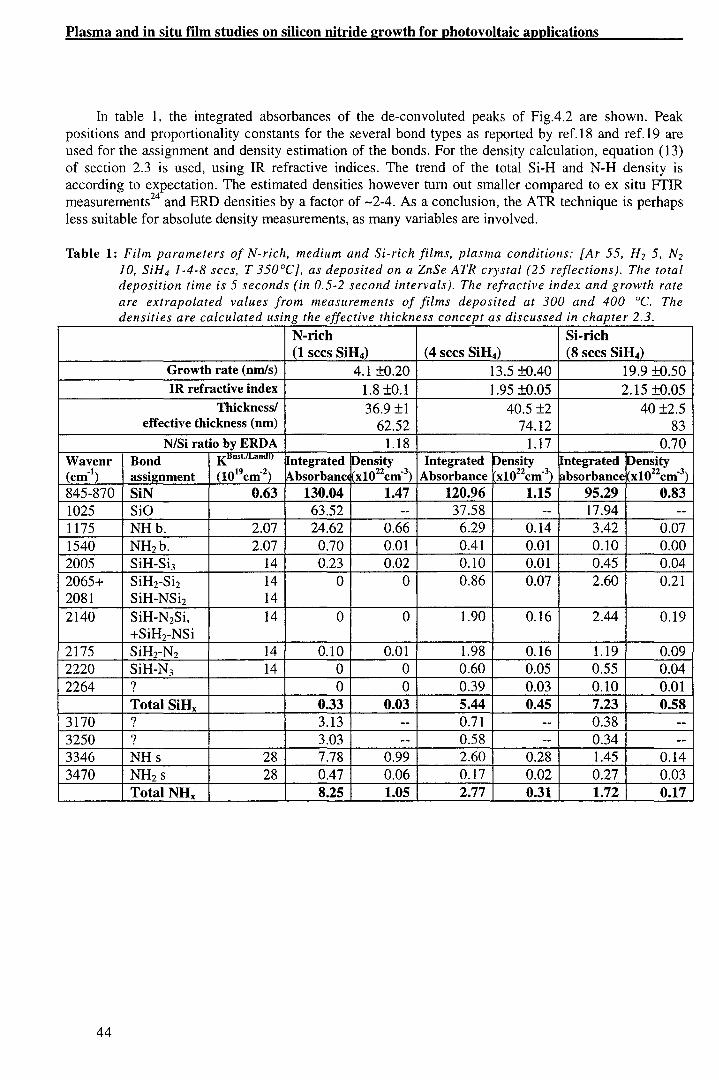
Plasma and in situ film studies on silicon nitride growth for photovoltaic applications
In table 1, the integrated absorbances of the de-convoluted peaks of Fig.4.2 are shown. Peak positions and proportionality constants for the several bond types as reported by ref.l8 and ref.19 are used for the assignment and density estimation of the bonds. For the density calculation, equation ( 13) of section 2.3 is used, using IR refractive indices. The trend of the total Si-H and N-H density is according to expectation. The estimated densities however turn out smaller compared to ex situ FTIR measurements24 and ERD densities by a factor of -2-4. As a conclusion, the ATR technique is perhaps less suitable for absolute density measurements, as many variables are involved.
Table 1: Film parameters of N-rich, medium and Si-rich films, plasma conditions: [Ar 55, H2 5, N2
JO, SiH4 1-4-8 sccs, T 350°C], as deposited on a ZnSe ATR crystal (25 reflections). The total deposition time is 5 seconds (in 0.5-2 second intervals). The refractive index and growth rate are extrapolated values from measurements of films deposited at 300 and 400 °C. The densities are calculated using the effective thickness concept as discussed in chapter 2.3.
N-rich Si-rich (1 sccs SiH4) ( 4 sccs SiH4) (8 sccs SiH4)
Growth rate (nrnls) 4.1 ±0.20 13.5 ±0.40 19.9 ±0.50 IR refractive index 1.8 ±0.1 1.95 ±0.05 2.15 ±0.05
Thickness/ 36.9 ±1 40.5 ±2 40 ±2.5 effective thickness (nm) 62.52 74.12 83
N/Si ratio by ERDA 1.18 1.17 0.70 Wavenr Bond KBustJLandl) ~ntegrated IDensity Integrated Density ~ntegrated IDensity (cm·') assignment (1019cm·2
) IAbsorbanc x1022cm"3) A bsorbanee xl022cm.3
) la bsorbanee x1022cm·1 845-870 SiN 0.63 130.04 1.47 120.96 1.15 95.29 0.83 1025 SiO 63.52 -- 37.58 -- 17.94 --1175 NHb. 2.07 24.62 0.66 6.29 0.14 3.42 0.07 1540 NHzb. 2.07 0.70 0.01 0.41 0.01 0.10 0.00 2005 SiH-Sh 14 0.23 0.02 0.10 0.01 0.45 0.04 2065+ SiHz-Sh 14 0 0 0.86 0.07 2.60 0.21 2081 SiH-NSh 14 2140 SiH-NzSi, 14 0 0 1.90 0.16 2.44 0.19
+SiH2-NSi 2175 SiHz-Nz 14 0.10 0.01 1.98 0.16 1.19 0.09 2220 SiH-N3 14 0 0 0.60 0.05 0.55 0.04 2264 ? 0 0 0.39 0.03 0.10 0.01
Total SiHx 0.33 0.03 5.44 0.45 7.23 0.58 3170 ? 3.13 -- 0.71 -- 0.38 --3250 ? 3.03 -- 0.58 -- 0.34 --3346 NHs 28 7.78 0.99 2.60 0.28 1.45 0.14 3470 NHzs 28 0.47 0.06 0.17 0.02 0.27 0.03
Total NHx 8.25 1.05 2.77 0.31 1.72 0.17
44
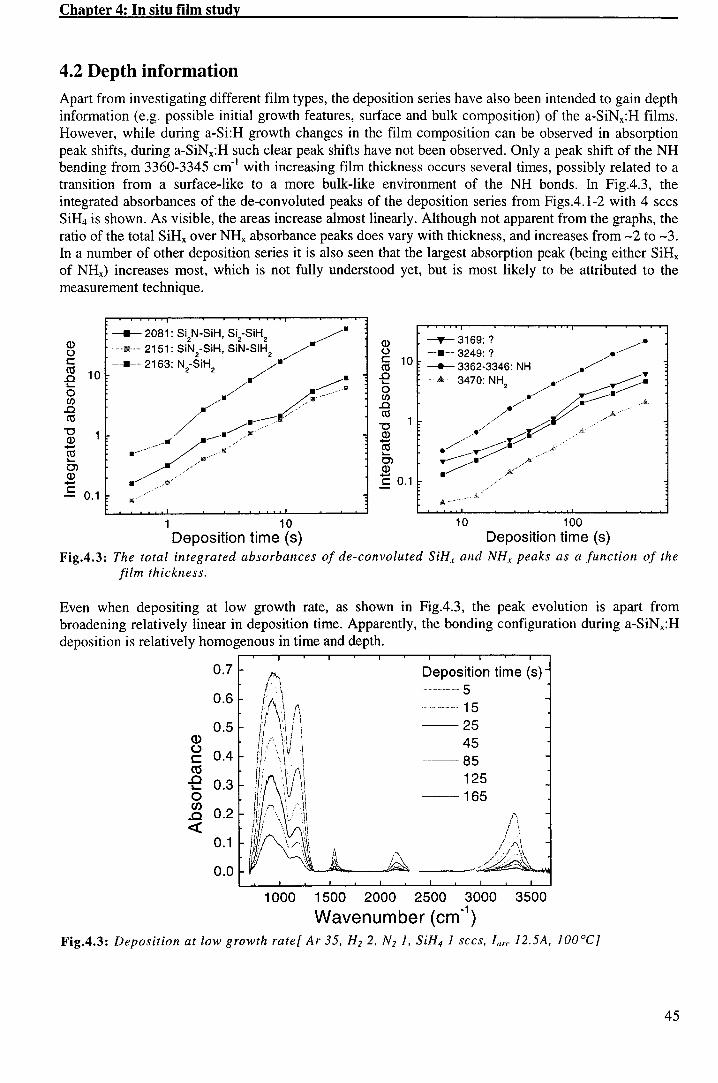
Chapter 4: In situ film study
4.2 Depth information Apart from investigating different film types, the deposition series have also been intended to gain depth information (e.g. possible initia! growth features, surface and bulk composition) of the a-SiNx:H films. However, while during a-Si:H growth changes in the film composition can be observed in absorption peak shifts, during a-SiNx:H such clear peak shifts have not been observed. Only a peak shift of the NH bending from 3360-3345 cm-1 with increasing film thickness occurs several times, possibly related to a transition from a surface-like to a more bulk-like environment of the NH bands. In Fig.4.3, the integrated absorbances of the de-convoluted peaks of the deposition series from Figs.4.1-2 with 4 sccs SiH4 is shown. As visible, the areas increase almast linearly. Although notapparent from the graphs, the ratio of the total SiHx over NHx absorbance peaks does vary with thickness, and increases from -2 to -3. In a number of other deposition series it is also seen that the largest absorption peak (being either SiHx of NHx) increases most, which is not fully understood yet, but is most likely to be attributed to the measurement technique.
..A· A··········
1 10 10 100 Deposition time (s) Deposition time (s)
Fig.4.3: The total integrated absorbances of de-convoluted SiHx and NHx peaks as a function of the film thickness.
Even when depositing at low growth rate, as shown in Fig.4.3, the peak evolution is apart from broadening relatively linear in deposition time. Apparently, the bonding configuration during a-SiN,:H deposition is relatively homogenous in time and depth.
0.7
0.6
0.5 Q) (.)
0.4 c <U .0 0.3 '-0 (J)
0.2 .0 <(
0.1
0.0 /\ ""--........,....__ __ ~
Deposition time (s) ·------ 5
. --- 15 --25
45 ·····--85
125 ---165
1000 1500 2000 2500 3000 3500
Wavenumber (cm-1)
Fig.4.3: Deposition at low growth ratel Ar 35, H2 2, N2 1, SiH4 1 sccs, 1arc 12.5A, 100°C]
45
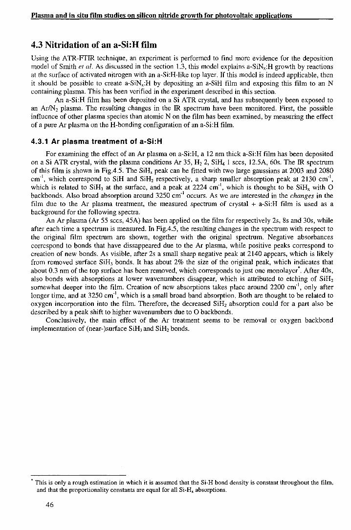
Plasma and in situ film studies on silicon nitride growth for photovoltaic applications
4.3 Nitridation of an a-Si:H film Using the ATR-FTIR technique, an experiment is performed to find more evidence for the deposition model of Smith et al. As discussed in the section 1.3, this model explains a-SiNx:H growth by reactions at the surface of activated nitrogen with an a-Si:H-like top layer. If this model is indeed applicable, then it should be possible to create a-SiNx:H by depositing an a-SiH film and exposing this film to an N containing plasma. This has been verified in the experiment described in this section.
An a-Si:H film has been deposited on a Si ATR crystal, and has subsequently been exposed to an Ar/N2 plasma. The resulting changes in the IR spectrum have been monitored. First, the possible influence of other plasma species than atomie N on the film has been examined, by measuring the effect of a pure Ar plasma on the H-bonding configuration of an a-Si:H film.
4.3.1 Ar plasma treatment of a-Si:H
For examining the effect of an Ar plasma on a-Si:H, a 12 nm thick a-Si:H film has been deposited on a Si ATR crystal, with the plasma conditions Ar 35, H2 2, SiH4 1 sccs, 12.5A, 60s. The IR spectrum of this film is shown in Fig.4.5. The SiHx peak can be fitted with two large gaussians at 2003 and 2080 cm· 1
, which correspond to SiH and SiH2 respectively, a sharp smaller absorption peak at 2130 cm· 1,
which is related to SiH3 at the surface, and a peak at 2224 cm·1, which is thought to be SiHx with 0
backbonds. Also braad absorption around 3250 cm-1 occurs. As we are interested in the changes in the film due to the Ar plasma treatment, the measured spectrum of crystal + a-Si:H film is used as a background for the following spectra.
An Ar plasma (Ar 55 sccs, 45A) has been applied on the film for respectively 2s, Ss and 30s, while aftereach time a spectrum is measured. In Fig.4.5, the resulting changes in the spectrum with respect to the original film spectrum are shown, tagether with the original spectrum. Negative absorbances correspond to bands that have dissappeared due to the Ar plasma, while positive peaks correspond to creation of new bands. As visible, after 2s a small sharp negative peak at 2140 appears, which is likely from removed surface SiH3 bands. It has about 2% the size of the original peak, which indicates that about 0.3 nm of the top surface has been removed, which corresponds to just one monolayer*. After 40s, also bonds with absorptions at lower wavenumbers disappear, which is attributed to etching of SiH2
somewhat deeper into the film. Creation of new absorptions takes place around 2200 cm-1, only after
longer time, and at 3250 cm·1, which is a small broad band absorption. Both are thought to be related to
oxygen incorporation into the film. Therefore, the decreased SiH2 absorption could for a part also be described by a peak shift to higher wavenumbers due to 0 backbonds.
Conclusively, the main effect of the Ar treatment seems to be remaval or oxygen backbond implementation of (near-)surface SiH3 and SiH2 bands.
• This is only a rough estimation in which it is assumed that the Si-H bond density is constant throughout the film, and that the proportionality constants are equal for all Si-H, absorptions.
46
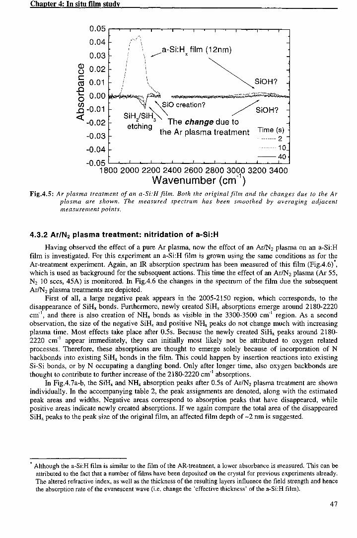
Chapter 4: In situ film study
0 . 0 5 r--r--r-.---,r--"'1.---,r--"'1-----r-----r-----r--,.---,-----r----,----.-----r---,
0.04
0.03
~ 0.02 c ~ 0.01 ..c
a-Si:H film (12nm) ~ x
~SiOH? 0 0.00 ~~-,~""""'·) ""' ~ _0_01 -; ,,>,SiO creation? ~iOH?
SiH /SiH.,"' '\-. / ~ <( -0.02 t 2h. 3 The change due to e c mg
_0_03 the Ar plasma treatment Time (s) -·---······-·2
-0.04 10 --40
-0.05 L-L-L--'--l....--.JL......--JL-.I~---...I~---'---l.--'-__....1.--'-__....I.___J 1 800 2000 2200 2400 2600 2800 3000 3200 3400
Wavenumber (cm-1)
Fig.4.5: Ar plasma treatment of an a-Si:H film. Both the original film and the changes due to the Ar plasma are shown. The measured spectrum has been smoothed by averaging adjacent measurement points.
4.3.2 Ar/N 2 plasma treatment: nitridation of a-Si:H
Having observed the effect of a pure Ar plasma, now the effect of an Ar/N2 plasma on an a-Si:H film is investigated. For this experiment an a-Si:H film is grown using the same conditions as for the Ar-treatment experiment. Again, an IR absorption spectrum has been measured of this film (Fig.4.6) *, which is used as background for the subsequent actions. This time the effect of an Ar/N2 plasma (Ar 55, N2 10 sccs, 45A) is monitored. In Fig.4.6 the changes in the spectrum of the film due the subsequent Ar/N2 plasma treatments are depicted.
First of all, a large negative peak appears in the 2005-2150 region, which corresponds, to the disappearance of SiHx bonds. Furthermore, newly created SiHx absorptions emerge around 2180-2220 cm-1
, and there is also creation of NHx honds as visible in the 3300-3500 cm-1 region. As a second observation, the size of the negative SiHx and positive NHx peaks do not change much with increasing plasma time. Most effects take place after 0.5s. Because the newly created SiHx peaks around 2180-2220 cm-1 appear immediately, they can initially most likely not be attributed to oxygen related processes. Therefore, these absorptions are thought to emerge solely because of incorporation of N backhonds into existing SiHx bonds in the film. This could happen by insertion reactions into existing Si-Si honds, or by N occupating a dangling bond. Only after longer time, also oxygen backhonds are thought to contribute to further increase of the 2180-2220 cm-1 absorptions.
In Fig.4.7a-b, the SiHx and NHx absorption peaks after 0.5s of Ar/N2 plasma treatment are shown individually. In the accompanying table 2, the peak assignments are denoted, along with the estimated peak areas and widths. Negative areas correspond to absorption peaks that have disappeared, while positive areas indicate newly created absorptions. lf we again cernpare the total area of the disappeared SiHx peaks to the peak si ze of the original film, an affected film depth of-2 nm is suggested.
• Although the a-Si:H film is similar to the film of the AR-treatment, a lower absorbance is measured. This can be attributed to the fact that a number of films have been deposited on the crystal for previous experiments already. The altered refractive index, as well as the thickness of the resulting layers influence the field strength and hence the absorption rate of the evanescent wave (i.e. change the 'effective thickness' of the a-Si:H film).
47
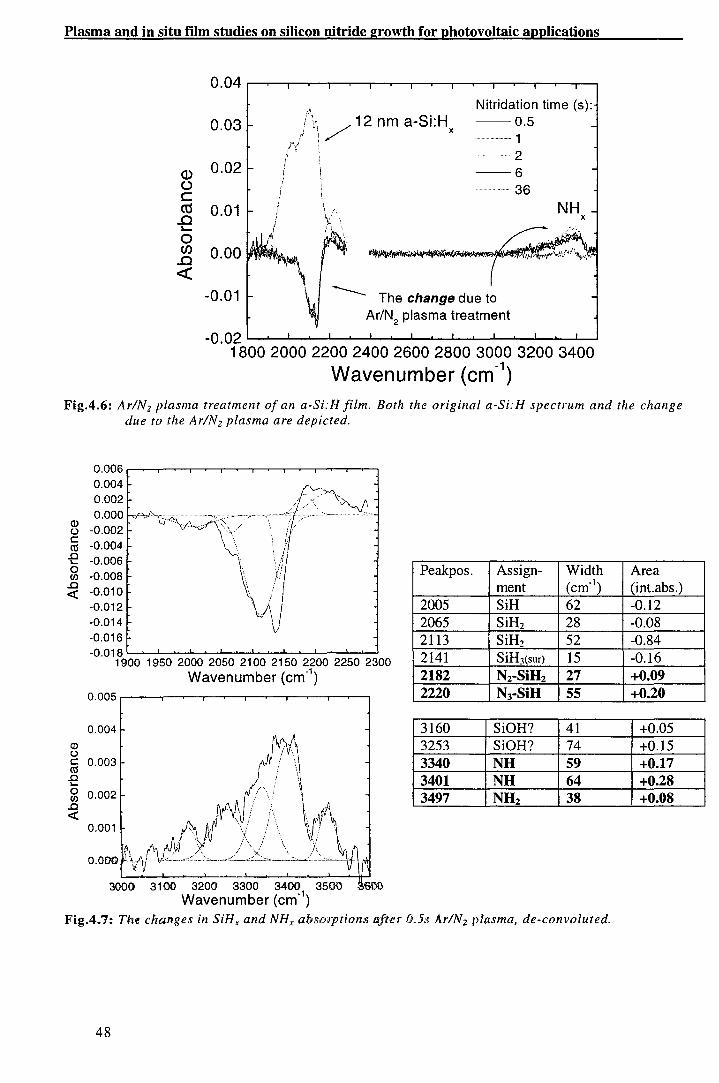
Plasma and in situ film studies on silicon nitride growth for photovoltaic applications
Q) (.) c ct! ..c '-0 en ..c <(
0.04
0.03
0.02
0.01
0.00
-0.01
/ 12 nm a-Si:Hx Nitridation time (s): --0.5
............... 1
2 --6
36
-- The change due to Ar/N
2 plasma treatment
NH x
-0. 02 '--L..........JL..........J'-----'-1.--L--1.----L--L.---L.--L.--'-----'-----'---'----'---l
1800 2000 2200 2400 2600 2800 3000 3200 3400
Wavenumber (cm-1)
Fig.4.6: Ar!N2 plasma treatment of an a-Si:H film. Both the original a-Si:H spectrum and the change due to the Ar!N2 plasma are depicted.
-0.01 8 L-..---'----'---'-~-'-~..L-~...__.___,___..___.___.__, 1900 1950 2000 2050 2100 2150 2200 2250 2300
Wavenumber (cm-1)
0.004
~ ~~\ ~ 0.003 rJi ! \\
-e ) / \\ ( /' ' '·I g 0.002 • (' / \, 1
.o f-i\vll /, \, ,l., <t: 1\. \ r ; ' ~{v ~" o.oo1 tl<'!; A· \! ! \ 1\ / '1
A I \' nJ 'f.. .· · , \ f!l. /Ir, N.Vi )! _ / \/ \ \ ~ n
0.000' I \fV· V·---"·<-- >~----·'--"~-.:."., __ .:0--é:-':·:-~ \ ~
'3000 31 00 3200 3300 3400 3500 i&'!(} -1
Wavenumber (cm )
Peakpos. Assign- Width ment (cm- 1
)
2005 SiH 62 2065 SiHz 28 2113 SiHz 52 2141 SiH3(sur) 15 2182 Nz-SiHz 27 2220 N3-SiH 55
3160 Si OH? 41 3253 SiOH? 74 3340 NH 59 3401 NH 64 3497 NHz 38
Fig.4.7: The changes in SiHx and NHx absmption.'i lAft-er 0.5.s Ar!N2 plasma, de-convoluted.
48
Area (int.abs.) -0.12 -0.08 -0.84 -0.16 +0.09 +0.20
+0.05 +0.15 +0.17 +0.28 +0.08
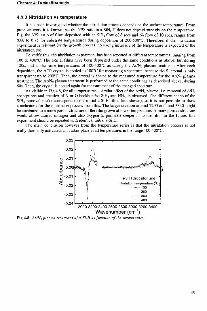
Chapter 4: In situ film study
4.3.3 Nitridation vs tempersture
It has been investigated whether the nitridation process depends on the surface temperature. From previous work it is known that the N/Si ratio in a-SiNx:H does not depend strongly on the temperature. E.g. the N/Si ratio of films deposited with an SiH4 flow of 8 sccs and N2 flow of 10 sccs, ranges from 0.66 to 0.75 for substrate temperatures during deposition of 200-500°C. Therefore, if the nitridation experiment is relevant for the growth process, no strong influence of the temperature is expected of the nitridation too.
To verify this, the nitridation experiment has been repeated at different temperatures, ranging from 100 to 400°C. The a-Si:H films have been deposited under the same conditions as above, but during 120s, and at the same temperatures of 100-400°C as during the Ar/N2 plasma treatment. After each deposition, the ATR crystal is cooled to l00°C for measuring a spectrum, because the Si crystal is only transparent up to 200°C. Then, the crystal is heated to the measured temperature for the Ar/N2 plasma treatment. The Ar/N2 plasma treatment is performed at the same conditions as described above, during 60s. Then, the crystal is cooled again for measurement of the changed spectrum.
As visible in Fig.4.8, for all temperatures a similar effect of the Ar/N2 plasma, i.e. remaval of SiHx absorptions and creation of N or 0 backbonded SiHx and NHx, is observed. The different shape of the SiHx removal peaks correspond to the initial a-Si:H films (not shown), so it is not possible to draw conclusions for the nitridation process from this. The larger creation around 2200 cm-1 and 3340 might be attributed to a more porous structure of the film grown at lower temperature. A more porous structure would allow atomie nitrogen and also oxygen to permeate deeper in to the film. In the future, this experiment should be repeated with identical initial a-Si:H.
The main condusion however from the temperature series is that the nitridation process is not really thermally activated, as it takes place at all temperatures in the range 100-400°C.
0.02
Q.) 0.01 (.) t: ctS
...c "_
g -0.01 ...c <( -0.02
-0.03
a-Si:H deposition and
nitridation temperature (C) 100 200
--300 400 -0.04 ......___,__.___.__.__.___.__.__.__.___.___.__.....__....__....___....__....._,
20002200240026002800300032003400 Wavenumber (cm-1
)
Fig.4.8: Ar/N2 plasma treatment of a-Si:H as function of the temperature.
49
Chapter 5: Conclusions
Chapter 5
Conclusions
A study has been performed on the feasibility of high-rate (-20 nm/s) deposited a-SiNx:H using the cascaded are generated expanding thermal plasma. By implementation of the films in multicrystalline silicon solar cells, promising antireflection and bulk passivating qualities have been demonstrated.
To support future optimization of the deposition process, a study is made on the a-SiNx:H growth process using a SiHJN2 plasma. As a starting point, a proposed growth model by Smith et al. has been used. In this model, the a-SiNx:H deposition process is portrayed by surface reactions in which an a-Si:H-like top layer, formed by a-Si:H depositing radicals, becomes 'nitridated' by activated nitrogen from the plasma. The densities of, on basis of available knowledge on the a-Si:H depositing plasma, viabie candidate species for the a-SiH-like layer formation and nitridation reactions have been measured.
Cavity ringdown spectroscopy (CRDS) has been applied to measure the densities of SiH3 and SiH radicals in the Ar/H2/SiHJN2 plasma. Threshold ionization mass speetrometry (TIMS) has been applied to measure N radical densities. From these densities and an estimated typical gas temperature deduced from the measured SiH rotational temperature of 1400K, an estimate is made of the individual contributions of SiH3, SiH and N radicals to the growth. These contributions are compared to the growth flux as obtained by composition measurements by ERD and measured deposition rates. From these studies, the following conclusions can be drawn:
• SiH3 has a high density in the plasma of-1-4·1019 m·\ while SiH has a density of -0.5-1-1017 m·3. At these densities, SiH3 can almast fully account for the Si growth flux, while SiH has a contribution in the order of percentages. The large contribution of SiH3 is reflected in the nearly linear dependenee of the Si incorporation rate to the SiH3 density, except at low SiH4 flows, where other growth precursors are becoming increasingly important.
• A very high atomie N density of -1019-1020 is measured in the Ar/H2/SiHJN2 plasma. This high density could well account for the N-incorporation rate in the a-SiNx:H films during deposition. The measured growth flux then indicates that the N radical has a sticking probability of -2%.
Besides, an in situ technique for infrared absorption measurements, attenuated total reflection Fourier transfarm infrared spectroscopy (ATR-FTIR), has been installed. This technique has been used to monitor the Si-N, Si-H and N-H bonding configurations of as-deposited films as a function of film thickness, to gain depth information of the films.
In addition, with the ATR-FTIR technique an experiment is performed to find more evidence for the proposed a-SiNx:H growth model of Smith. If this model is applicable, it should be possible to create a-SiNx:H at the surface of an a-Si:H film, by modifying the a-Si:H film with a N-containing plasma. This has been verified in a 'nitridation' experiment, in which an as-deposited a-Si:H film has been exposed to an Ar/N2 plasma. From these studies the following conclusions can be drawn:
• The monitored IR absorptions during series of short subsequent a-SiNx:H depositions, do not exhibit large peak shifts and increase nearly linear with time. This suggests a relative homogeneaus growth of a-SiNx:H in time and depth as far asthebonding configuration is concemed.
• It is demonstrated that a-SiNx:H can be created by exposing a-Si:H to an Ar/N2 plasma. The measured changes in the infrared absorption spectrum suggest that the plasma treatment results in the creation of an a-SiNx:H surface layer with adepthof -2 nm. This 'nitridation' process doesnotshow a large dependenee on the substrate temperature within the range of 1 00-400°C, which supports the relevancy of this experiment to a-SiNx:H deposition, where no large temperature dependenee of the N/Si ratio is observed either. As a conclusion, bath the plasma studies and the nitridation experiment corroborate the proposed aSiNx:H growth model of Smith et al.. As an extension to this model, the measured radical densities in the plasma indicate that the formation of the a-Si:H-Iike layer can almost fully be accounted for by SiH3 radicals, while the role of the activated nitrogen could well be filled in by the N radical.
51
Uankwoord
Dankwoord
Een woord van dank gaat uit naar alle mensen in de ETP groep, zonder wie mijn afstudeerwerk natuurlijk nooit mogelijk was geweest. Allereerst bedank ik mijn directe begeleider Erwin Kessels. Zijn fenomenale drive en kennis van zaken waren een belangrijke bron van inspiratie, zeker op sommige latere momenten waarop het heilige vuur (het heilige plasma) wat tanende was bij mij. Ik heb als ik terugkijk veel plezier gehad, en zeer veel gezien en geleerd. Verder natuurlijk dank voor mijn indirecte begeleider Richard van de Sanden, voor de mooie gelegenheden die hij mij geboden heeft om te komen afstuderen, en eerder ook de stage in Albany. Also thanks to Junegie Hong, for the pleasant daily cooperation, enthusiastic support and provided knowledge during my project. I wish you and Hyelim the very best with your new life with your daughter. Onontbeerlijk waren de technische ondersteuning en raadgeving van Ries en Herman, met name tijdens het opbouwen van de A TR meetopstelling, en Bertus hulp als er iets mis ging met de besturing tijdens het meten. Dat geldt ook voor de administratieve ondersteuning van Jeanne en de vele AIO's die ik heb lastig gevallen met vragen, met name Arno, Karine, Adriana, Johan, en Maikel, maar iedereen is wel eens aan bod geweest. Speciale dank voor Johan en Alquin voor de SiH metingen en advies tijdens het uitwerken van die metingen. Ik mag ook niet onvermeld laten de genereuze hulp die ik op de valreep kreeg van Jean-Pierre met advies over de samenvatting en bij het weer "even" opzoeken van de laatste referenties in dit verslag. Ook de belangstelling van Daan Schram is gewaardeerd. Tenslotte natuurlijk dank voor de gezellige samenwerking met mijn (voorheen) medestudenten Arjen, Alquin, Jean-Pierre, Yolanda, Peter en Bram, en de hele nieuwe lichting studenten die ik niet allemaal bij naam ga vermelden, maar het wordt in ieder geval steeds gezelliger en knusser in kamer 1.73. OK, jullie mogen mijn bureau nu helemaal hebben.
53
References
References
Donald L. Smith, Andrew S. Alimonda, and Frederick J. von Preissig, J.Vac.Sci.Technol. B 8, p551 (1990)
2 Donald L. Smith, Mat.res.soc.Proc.Vol.165, p69 (1990) Bengi F. Hanyaloglu and Eray S.Aydil, J.Vac.Sci.Technol. A 16, p2794 (1998)
4 W.M.M. Kessels, A.Leroux, M.G.H. Boogaarts, J.P.M. Hoefnagels, M.C.M.van de Sanden, and D.C. Schram, J.Vac.Sci.Technol. A 19, p467 (2001)
5 W.M.M. Kessels, J.P.M. Hoefnagels, M.G.H. Boogaarts, D.C.Schram, and M.C.M.van de Sanden, J.Vac.Sci.Technol. A 19, p1027 (2001)
6 J .P.M.Hoefnagels, Cavity ringdown study of the densities and kinetics of SiHx radicals in a remote SiH4 plasma, Master Thesis, Technica! University Eindhoven (Aug.2000)
7 K.W. Busch and M.A. Busch (Eds.), Cavity-Ringdown Spectroscopy: An ultratrace-Absorption Measurement Technique, American Chemica! Society, Washington, DC (1999)
8 R.D. Johnson, B.P. Tsai, and J.W. Hudgens, J. Chem. Phys. 91, 3340 (1989) 9 P.D. Lightfood, R. Becerra, A.A. Jemi-Alade, and R. Lescleaux, Chem. Phys. Lett. 180, 441
(1991) 10 J. Luque and D.R. Crosley, Lifbase: Database and Speetral Simulation Program (version 1.5), SRI
International report MP 99-009 (1999) 11 W.M.M. Kessels, M.C.M. van de Sanden, and D.C. Schram, J. Vac. Sci. Techno!. A 18, (2000) 12 W.M.M. Kessels, J.P.M. Hoefnagels, M.G.H. Boogaarts, D.C.Schram, and M.C.M.van de Sanden,
J.Appl.Phys 13 Harmeet Singh, J.W.Coburn, and David B.Graves, J.Vac.Sci.Technol. A 18, p299 (2000) 14 H.C.Straub, P.Renault, B.G.Lindsay, K.A.Smith, and R.F.Stebbings, Phys.Rev. A 54, (1995) 15 D.Rapp, P.Englander-Golden and D.D. Briglia, J.Chem.Phys.42 16 T.D.Märk, and T.H.Dunn, Electron impact ionization, Springer-Verlag Wien-New York, p292
(1985) 17 N.J. Harrick, Internat Rejlection Spectroscopy, Philips Laboratories, Briarcliff Manor, New York
(1967) 18 E. Bustarret, M. Bensouda, M.c. Habrard, and J.C. Bruyère, Phys.Rev. A 38, p8171 ( 1988) 19 W.A.Lanford and M.J.Rand, J.Appl.Phys 49 p2473 (1978) 20 W.M.M.Kessels, C.M.Leeuwis, M.C.M.van de Sanden, D.C. Schram, J.Appl.Phys.86, p4029
(1999) 23
24
25
26
27
28
29
30
Christian M. Leeuwis, Radical and Jon Measurements in an Expanding Ar/H2/SiH4 Plasma, Master Thesis, Technica} University Eindhoven (Oct 1998) W.M.M.Kessels, J.Hong, F.J.H.v.Assche, J.D. Moshner, T.Lauinger, W.J. Soppe, A.W. Weeber, D.C. Schram, and M.C.M. van de Sanden, High-rate deposition of a-SiN.r-H for photovoltaic applications by the expanding thermal plasma (2002) Stephane Mazoufre et al., not published P. Kae-Nune, J. Perrin, J. Guillon, and J. Jolly, Plasma Sourees Sci. Technol. 4, 250 (1995). W.M.M.Kessels, Patriek R. McCurdy, Keri K. Williams, G.R. Barker, Vincent A. Venturo, and Ellen R.Fisher, J. Phys. Chem B 106, p2680 (2002) K. Stephan, H. Helmand T.D. Mark, J.Chem.Phys. 73, p3763 (1980) Adams, Milier Harmeeth Singh, J.W.Coburn, and David B.Graves, J.appl.physics 88, p3748 (2000)
55
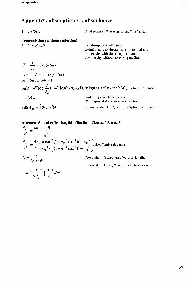
Appendix
Appendix: absorption vs. absorbance
I= T+R+A
Transmission (without reflection): I = I0 exp( -ad)
I T =- = exp(-ad)
Io A= I-T = 1-exp(-ad) A:::::: ad, if ad<<l
A=absorption, T=transmission, R=reflection
a =absorption coefficient, d=light pathway through absorbing medium, l=intensity with absorbing medium, lo=intensity without absorbing medium
I Abs =-10 log(-) =-10 log(exp(-ad)) = log(e) ·ad= ad I 2.30, Abs=absorbance
Io n=density absorbing species, K=reciprocal absorption cross section
with Aim =I am-1 dm A;nt=normalized integrated absorption coefficient
Attenuated total reflection, thin film limit (2ru:I<O.l·À, k<O.l)
4n21 cose. 2 '
(1-nJJ )
dett 4n21 cos8((1+n324)sin
28-n31
2J .. -- = 2 2 . 2 2 , d,=effectlve thtckness d (1- n31 ) (1 + n31 ) sm e - n31
N = l N=number of reflections, l=crystal length, 2ttan8'
n = 2.30 · K I Abs dm Nde m
t=crystal thickness, B=angle to surface normal
57