Embed Size (px)
Citation preview
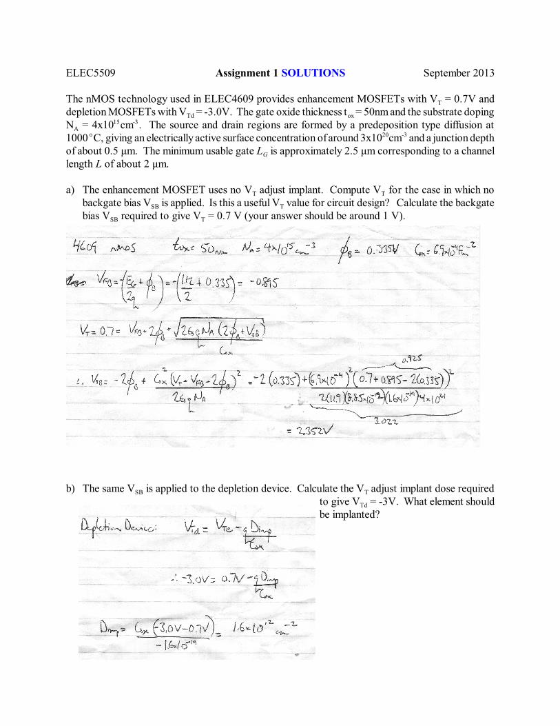
ELEC5509 Assignment 1 SOLUTIONS September 2013
TThe nMOS technology used in ELEC4609 provides enhancement MOSFETs with V = 0.7V and
Td oxdepletion MOSFETs with V = -3.0V. The gate oxide thickness t = 50nm and the substrate doping
AN = 4x10 cm . The source and drain regions are formed by a predeposition type diffusion at15 -3
1000EC, giving an electrically active surface concentration of around 3x10 cm and a junction depth20 -3
Gof about 0.5 ìm. The minimum usable gate L is approximately 2.5 ìm corresponding to a channellength L of about 2 ìm.
T Ta) The enhancement MOSFET uses no V adjust implant. Compute V for the case in which no
SB Tbackgate bias V is applied. Is this a useful V value for circuit design? Calculate the backgate
SB Tbias V required to give V = 0.7 V (your answer should be around 1 V).
SB Tb) The same V is applied to the depletion device. Calculate the V adjust implant dose required
Tdto give V = -3V. What element shouldbe implanted?

c) For this part and all subsequent parts, use MINIMOS. An example MINIMOS input file for theenhancement transistor is provided on the course website. The source/drain diffusion parametershave been adjusted arbitrarily to approximate the actual doping profile. Run MINIMOS and thenPostmini to plot the doping profile for the device. Confirm that the source/drain junction depthis close to 0.5 ìm.
Black dashed line shows metallurgical junction (depth a bit more than 0.5 ìm)
T Td) Determine V for a long channel device (L = 10 ìm). Next find the value of L for which V drops100mV below the long channel value. Use OPTION MODEL=THRESH for this part.
I Tnput file to determine V for L = 10 ìm:
Carleton nMOSDEVICE CHANNEL=N GATE=NPOLY TOX=50E-7 W=1.0E-4 L=10.0E-4PROFILE NS=3E20 TEMP=1080 TIME=600 NB=4E15 OPTION MODEL=THRESH PHYSCHK=NO CU=1E-7BIAS UD=0.1 UG=0 UB=-1OUTPUT PSI=N ETRAN=N ELAT=N MIN=N DC=N AVAL=NEND ERR=0.001 BIN=Y
TSetting UB=-1 gives V = 816 mV (note this doesn’t agree very well with calculation in (b), butELEC4609 students may recall it is actually very close to the experimental value)Use this value of UB in subsequent simulations
TReducing L to 6 ìm drops V to 706 mV (onset of short channel effects)

DSe) Determine S for L = 10 ìm. Set V = 100mV.
TEasy way: use the Minimos program above to find V , but run for CU=1E-9 and CU=1E-10
DFor I = 10 nA VGS= 574 mV
DFor I = 1 nA VGS= 477mV
So S is 97 mV/decade (fairly typical of bulk CMOS)
DIBL DIBL DSf) Determine the value of L for which V = 200mV. Compute V between V = 0.1V and
DS DV = 5V. A quick way to do this is to use MODEL=THRESH, but set the value of I definingthreshold to a very low value (e.g. 1 nA/ìm).
T D DUse the “find V “ input file above, with CU=1E-9. Run for V = 0.1V and V = 5V and take the
GS DIBL DIBLdifference in V . This is V . Start with L = 10 ìm then reduce L; V gets bigger.
DIBL L = 10 ìm V = 12 mV
DIBL L = 2.5 ìm V = 115 mV
DIBL L = 2 ìm V = 240 mV
So the answer is around L = 2 ìm
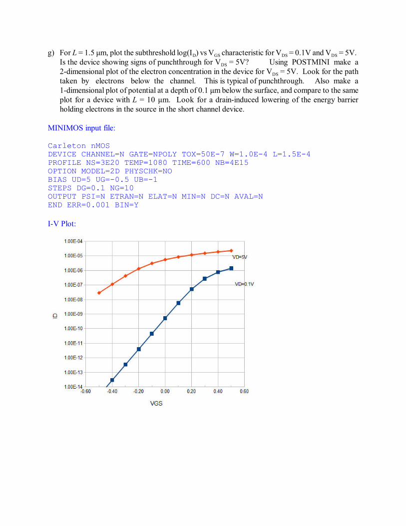
D GS DS DSg) For L = 1.5 ìm, plot the subthreshold log(I ) vs V characteristic for V = 0.1V and V = 5V.
DSIs the device showing signs of punchthrough for V = 5V? Using POSTMINI make a
DS2-dimensional plot of the electron concentration in the device for V = 5V. Look for the pathtaken by electrons below the channel. This is typical of punchthrough. Also make a1-dimensional plot of potential at a depth of 0.1 ìm below the surface, and compare to the sameplot for a device with L = 10 ìm. Look for a drain-induced lowering of the energy barrierholding electrons in the source in the short channel device.
MINIMOS input file:
Carleton nMOSDEVICE CHANNEL=N GATE=NPOLY TOX=50E-7 W=1.0E-4 L=1.5E-4PROFILE NS=3E20 TEMP=1080 TIME=600 NB=4E15 OPTION MODEL=2D PHYSCHK=NOBIAS UD=5 UG=-0.5 UB=-1STEPS DG=0.1 NG=10OUTPUT PSI=N ETRAN=N ELAT=N MIN=N DC=N AVAL=NEND ERR=0.001 BIN=Y
I-V Plot:

Electron plot: Energy barrier plot:

DS GSh) Run a simulation in saturation (V = 5V, V -= 2V) for a device with L = 2 ìm. UseMODEL=AVAL. Using Postmini make 2-dimensional plots of the electron concentration andelectron current. Identify the “pinch off point”, the point in the depletion region near the drainwhere the electron concentration drops below the dopant ion concentration. Observe how theelectron current breaks away from the surface at the pinch-off point, entering the drain below thesurface.
MINIMOS input file:
Carleton nMOSDEVICE CHANNEL=N GATE=NPOLY TOX=50E-7 W=1.0E-4 L=2.0E-4PROFILE NS=3E20 TEMP=1080 TIME=600 NB=4E15 OPTION MODEL=AVAL PHYSCHK=NO BIAS UD=5 UG=2.0 UB=-1OUTPUT PSI=N ETRAN=N ELAT=N MIN=N DC=N AVAL=NEND ERR=0.001 BIN=Y
Electron concentration plot:

DS GSi) For L = 2 ìm, fix V at 5V and find the value of V giving peak substrate current. Again use
GSMODEL=AVAL. For this value of V , use Postmini to make 2-dimensional plots of the lateralelectric field and the generation rate. Where is the generation rate highest?
Peak substrate current found at VG = 1.5 V:
VG: IB:1.2 V 4.6e-10 A/ìm1.4 4.9e-101.5 4.9e-101.6 4.8e-101.7 4.7e-101.8 4.5e-10
Lateral Electric Field: Avalanche Generation Rate:

j) Write a MINIMOS input file for the depletion transistor. Implant phosphorus at 60 keV to set
Td Td SBV . Adjust the dose so that V = -3V for the value of V found in (a).
Carleton nMOSDEVICE CHANNEL=N GATE=NPOLY TOX=50E-7 W=1.0E-4 L=5.0E-4PROFILE NS=3E20 TEMP=1080 TIME=600 NB=4E15 IMPLANT ELEM=P DOSE=1.5E12 AKEV=60 TEMP=1080 TIME=600OPTION MODEL=THRESH PHYSCHK=NO CU=1E-7BIAS UD=0.1 UG=0 UB=-1OUTPUT PSI=N ETRAN=N ELAT=N MIN=N DC=N AVAL=NEND ERR=0.001 BIN=Y
TdThis gives V = -2.9 V
k) Using MINIMOS, compare short channel effects in the enhancement and depletion transistors forL = 2 ìm. Why does the depletion transistor show stronger short channel effects?
Subthreshold I-V for enhancement and depletion transistors:

Depletion transistor is a buried channel device, which gives worse short channel effects
For VG=-3V (onset of threshold), note how potential well where electrons gather forms belowsurface; also note electron concentration peak below surface