Embed Size (px)
Citation preview
ARTICLE IN PRESS
1369-8001/$ - se
doi:10.1016/j.m
�Correspondfax: +49721 60
E-mail addr
(D. Gerthsen).
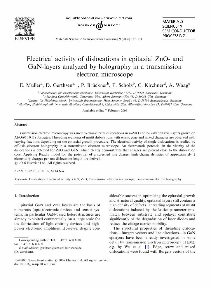
Materials Science in Semiconductor Processing 9 (2006) 127–131
Electrical activity of dislocations in epitaxial ZnO- andGaN-layers analyzed by holography in a transmission
electron microscope
E. Mullera, D. Gerthsena,�, P. Brucknerb, F. Scholzb, C. Kirchnerd, A. Waagc
aLaboratorium fur Elektronenmikroskopie, Universitat Karlsruhe (TH), D-76128 Karlsruhe, GermanybAbteilung Optoelektronik, Universitat Ulm, Albert-Einstein-Allee 45, D-89081 Ulm, Germany
cInstitut fur Halbleitertechnik, Universitat Braunschweig, Hans-Sommer-StraX e 66, D-38106 Braunschweig, GermanydAbteilung Halbleiterphysik (now with Abteilung Optoelektronik), Universitat Ulm, Albert-Einstein-Allee 45, D-89081 Ulm, Germany
Available online 7 February 2006
Abstract
Transmission electron microscopy was used to characterize dislocations in n-ZnO and n-GaN epitaxial layers grown on
Al2O3(0 0 0 1) substrates. Threading segments of misfit dislocations with screw, edge and mixed character are observed with
varying fractions depending on the epitaxial growth procedure. The electrical activity of single dislocations is studied by
off-axis electron holography in a transmission electron microscope. An electrostatic potential in the vicinity of the
dislocations is detected for ZnO and GaN, which clearly demonstrates that charges are present close to the dislocation
core. Applying Read0s model for the potential of a screened line charge, high charge densities of approximately 2
elementary charges per nm dislocation length are derived.
r 2006 Elsevier Ltd. All rights reserved.
PACS: 61.72.Ff; 61.72.Lk; 61.14.Nm
Keywords: Dislocations; Electrical activity; GaN; ZnO; Transmission electron microscopy; Transmission electron holography
1. Introduction
Epitaxial GaN and ZnO layers are the basis ofnumerous (opto)electronic devices and sensor sys-tems. In particular GaN-based heterostructures arealready exploited commercially on a large scale forthe fabrication of light-emitting devices and high-power electronic amplifiers. However, despite con-
e front matter r 2006 Elsevier Ltd. All rights reserved
ssp.2006.01.047
ing author. Tel.: +49721 608 3200;
8 3271.
ess: [email protected]
siderable success in optimizing the epitaxial growthand structural quality, epitaxial layers still contain ahigh density of defects. Threading segments of misfitdislocations induced by the lattice-parameter mis-match between substrate and epilayer contributesignificantly to the degradation of laser diodes andreduce the charge carrier mobility.
The structural properties of threading disloca-tions—Burgers vectors and line directions—in GaNepilayers have been already investigated in somedetail by transmission electron microscopy (TEM),e.g. by Wu et al. [1]. Edge, screw and mixeddislocations were found with Burgers vectors of the
.
ARTICLE IN PRESSE. Muller et al. / Materials Science in Semiconductor Processing 9 (2006) 127–131128
type 13o1 1 2 04, o0 0 0 14 and 1
3o1 1 2 34 as
expected for materials occurring in the wurtzitestructure. The dislocation lines are oriented pre-dominantly along the [0 0 0 1]-growth direction. Thefractions of different dislocation types depend onthe parameters during epitaxial growth. Compar-able morphologies were observed for threadingdislocations in ZnO epilayers [2].
It has been known for many years that (band-like) electronic states in the energy gap arefrequently associated with dislocations in semicon-ducting materials. This topic was reviewed alreadyin 1991 by Alexander and Teichler [3]. Chargeddislocations were investigated up to the recent pastonly by averaging techniques as e.g. Hall mobilitymeasurements. Look et al. [4] analyzed the Hallmobility of GaN samples containing dislocationswith a density of 108 and 2� 1010 cm�2. Assuming 1acceptor state per c-lattice parameter along thedislocation line they obtained a good agreementbetween experimental data and calculated values.The only information that is available on the chargeof dislocations in ZnO was published by Osip’yanet al. [5] who applied charge measurements duringplastic deformation to analyze electrical chargesassociated with dislocations in bulk n-ZnO. Theydeduced a line charge of approximately 2 elemen-tary charges per nm. In contrast to threadingdislocations in epitaxial layers glissile dislocations,which are generated during plastic deformation aremainly oriented on (0 0 0 1) basal planes.
The electrical activity of individual dislocationsbecame accessible only recently when Cherns andLiao [6] applied electron holography in a transmis-sion electron microscope to detect the electrostaticpotential Vdis in the vicinity of single dislocations inGaN which could be associated with a negativelycharged dislocation core in n-GaN. The reconstruc-tion of the phase shift of the electron wave f, whichis measured with respect to the phase of a referencewave, allows the measurement of Vdis on the basis ofEq. (1) (see e.g. [7])
f ¼ CE
Z t
0
V0 þ Vdis ~rð Þð Þdz, (1)
where V0 is the mean inner Coulomb potential ofthe material and CE an electron-energy-dependentconstant. The integration has to be performed alongthe electron-beam direction over the sample thick-ness t. It has to be emphasized that Eq. (1) is onlyvalid if kinematical diffraction conditions areapplied because dynamical diffraction conditions
impose additional phase shifts. The electrostaticpotential Vdis results from the interaction of thecharges at the dislocation core. These charges arescreened by a space-charge region of opposite signto obtain overall neutrality of the dislocation core/space charge cylinder configuration. The local bandstructure is shifted according to the value and shapeof Vdis in the vicinity of the dislocation.
In the present work we have analyzed theelectrical activity of individual dislocations inn-ZnO and n-GaN epilayers using TEM combinedwith off-axis electron holography. The study wasmotivated partially by the difficulty to obtainp-conducting ZnO because charged dislocations donot only reduce the charge-carrier mobility but canalso provide a high density of electronic states if thedislocation density is high as in the case of epitaxialn-ZnO layers. This contribution needs to be takeninto account in the overall charge balance of thematerial. Another motivation was the assessmentand improvement of the accuracy for the measure-ment of Vdis and the quantitative evaluation of thedislocation line charge density.
2. Experimental techniques
All investigated samples were grown by low-pressure metal organic vapor phase epitaxy(MOVPE) on Al2O3(0 0 0 1) substrates. The ZnOlayer was deposited on an Al2O3(0 0 0 1) substratewith 40 nm GaN as a buffer layer between thesubstrate and the ZnO. Tertiary butanol anddiethylzinc were used as precursors for the ZnOgrowth with a VI/II-flux ratio of 12 at total reactorpressure of 200mbar and hydrogen as a carrier gas.The substrate temperature was 500 1C.
The GaN layer was deposited at 1125 1C on alow-temperature AlN nucleation layer using thestandard precursors TMGa, TMAl, and NH3.Silane was used as n-type dopant source. By vander Pauw Hall effect measurements, we determineda carrier concentration of 2� 1019 cm�3 and amobility of 116 cm2/Vs.
The TEM investigations were carried out in a200 keV Philips CM 200 FEG/ST microscope whichis equipped with a field emission gun. The disloca-tion Burgers vectors b were analyzed on the basis ofthe bg ¼ 0 extinction criterion using differentimaging vectors g. The weak-beam technique wasapplied to improve the resolution compared toconventional bright- and dark-field images (see e.g.[8]). Cross-section samples along the o1 1 0 04- and
ARTICLE IN PRESS
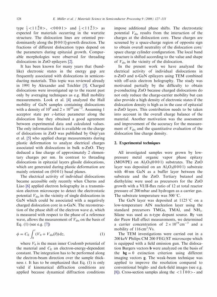
Fig. 1. Schematic drawing illustrating the interaction of a plane
electron wave with a thin TEM sample containing a charged
dislocation. (a) electron wave before transmission through the
sample, (b) electron wave after transmission through the sample
showing a distortion of the phase in the region of a charged
dislocation.
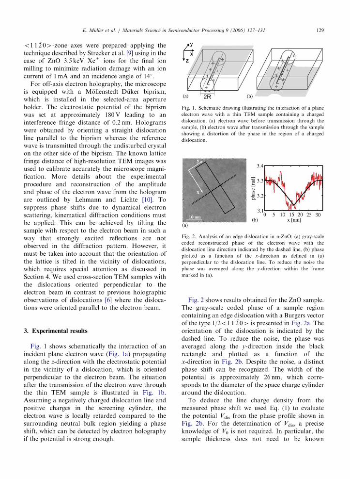
Fig. 2. Analysis of an edge dislocation in n-ZnO: (a) gray-scale
coded reconstructed phase of the electron wave with the
dislocation line direction indicated by the dashed line, (b) phase
plotted as a function of the x-direction as defined in (a)
perpendicular to the dislocation line. To reduce the noise the
phase was averaged along the y-direction within the frame
marked in (a).
E. Muller et al. / Materials Science in Semiconductor Processing 9 (2006) 127–131 129
o1 1 2 04-zone axes were prepared applying thetechnique described by Strecker et al. [9] using in thecase of ZnO 3.5 keV Xe+ ions for the final ionmilling to minimize radiation damage with an ioncurrent of 1mA and an incidence angle of 141.
For off-axis electron holography, the microscopeis equipped with a Mollenstedt–Duker biprism,which is installed in the selected-area apertureholder. The electrostatic potential of the biprismwas set at approximately 180V leading to aninterference fringe distance of 0.2 nm. Hologramswere obtained by orienting a straight dislocationline parallel to the biprism whereas the referencewave is transmitted through the undisturbed crystalon the other side of the biprism. The known latticefringe distance of high-resolution TEM images wasused to calibrate accurately the microscope magni-fication. More details about the experimentalprocedure and reconstruction of the amplitudeand phase of the electron wave from the hologramare outlined by Lehmann and Lichte [10]. Tosuppress phase shifts due to dynamical electronscattering, kinematical diffraction conditions mustbe applied. This can be achieved by tilting thesample with respect to the electron beam in such away that strongly excited reflections are notobserved in the diffraction pattern. However, itmust be taken into account that the orientation ofthe lattice is tilted in the vicinity of dislocations,which requires special attention as discussed inSection 4. We used cross-section TEM samples withthe dislocations oriented perpendicular to theelectron beam in contrast to previous holographicobservations of dislocations [6] where the disloca-tions were oriented parallel to the electron beam.
3. Experimental results
Fig. 1 shows schematically the interaction of anincident plane electron wave (Fig. 1a) propagatingalong the z-direction with the electrostatic potentialin the vicinity of a dislocation, which is orientedperpendicular to the electron beam. The situationafter the transmission of the electron wave throughthe thin TEM sample is illustrated in Fig. 1b.Assuming a negatively charged dislocation line andpositive charges in the screening cylinder, theelectron wave is locally retarded compared to thesurrounding neutral bulk region yielding a phaseshift, which can be detected by electron holographyif the potential is strong enough.
Fig. 2 shows results obtained for the ZnO sample.The gray-scale coded phase of a sample regioncontaining an edge dislocation with a Burgers vectorof the type 1/2o1 1 2 04 is presented in Fig. 2a. Theorientation of the dislocation is indicated by thedashed line. To reduce the noise, the phase wasaveraged along the y-direction inside the blackrectangle and plotted as a function of thex-direction in Fig. 2b. Despite the noise, a distinctphase shift can be recognized. The width of thepotential is approximately 26 nm, which corre-sponds to the diameter of the space charge cylinderaround the dislocation.
To deduce the line charge density from themeasured phase shift we used Eq. (1) to evaluatethe potential Vdis from the phase profile shown inFig. 2b. For the determination of Vdis, a preciseknowledge of V0 is not required. In particular, thesample thickness does not need to be known
ARTICLE IN PRESSE. Muller et al. / Materials Science in Semiconductor Processing 9 (2006) 127–131130
accurately because the integration in Eq. (1) has tobe carried out only over the diameter of the space-charge cylinder 2R. The interaction constant CE inEq. (1) is 7.29� 106 radV�1m�1 for our microscope[11]. According to Read [12] the electrostaticpotential of a screened line charge is given byEq. (2),
VdisðrÞ ¼�qe
4pee0ln
r2
R2
� ��
r2
R2
� �þ 1
� �, (2)
where q is the line charge density and r the distancefrom the dislocation core. The radius of the spacecharge cylinder R ¼
ffiffiffiffiffiffiffiffiffiffiffiffiffiffiq=pNs
pis determined by q
und the density of the compensating charges Ns,which are available for screening. For dislocationstates with acceptor character in n-type semicon-ductors, Ns is given by the density of uncompen-sated donors in the vicinity of dislocations. Theelectrical permittivity e was taken to be 7.8 for ZnO[13] and 9.5 for GaN [14]. Since the value of Ns forthe ZnO layer is unknown, we treat q and Ns as fitparameters. The line in Fig. 2b represents the best fiton the basis of Eqs. (1,2) which yields a line chargedensity of approximately 1.7 (elementary charges)nm�1 and Ns ¼ 3.3� 1018 cm�3.
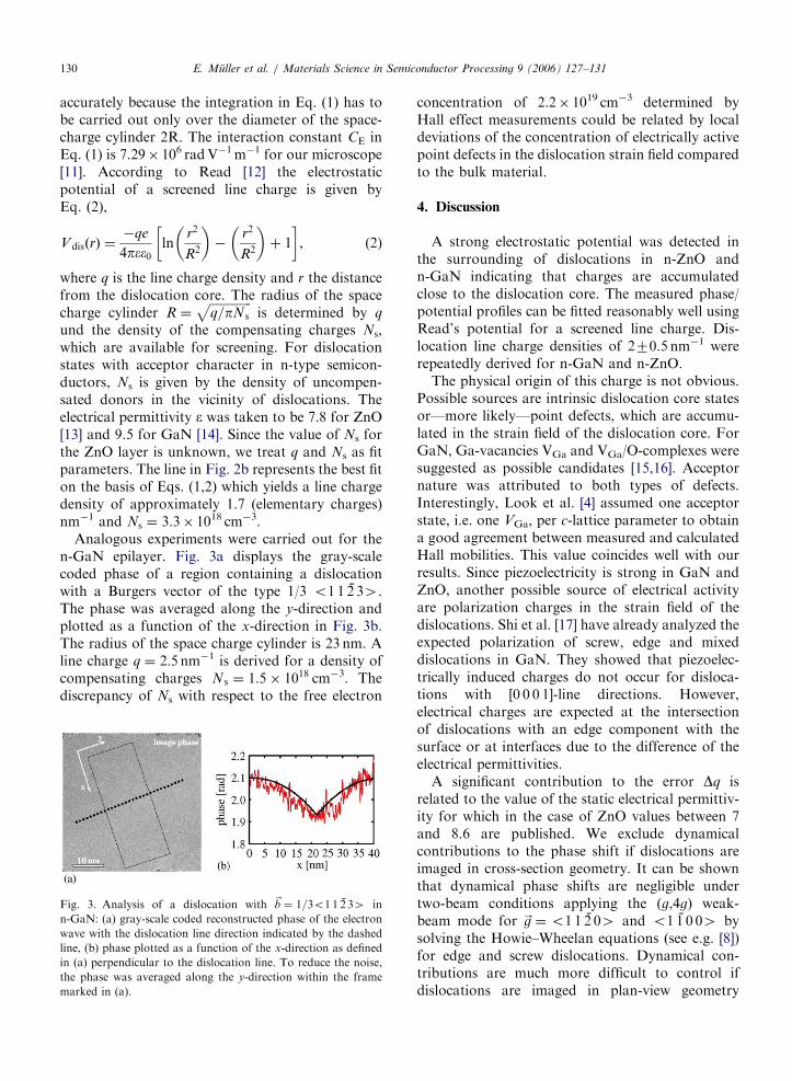
Analogous experiments were carried out for then-GaN epilayer. Fig. 3a displays the gray-scalecoded phase of a region containing a dislocationwith a Burgers vector of the type 1/3 o1 1 2 34.The phase was averaged along the y-direction andplotted as a function of the x-direction in Fig. 3b.The radius of the space charge cylinder is 23 nm. Aline charge q ¼ 2:5 nm�1 is derived for a density ofcompensating charges Ns ¼ 1:5� 1018 cm�3. Thediscrepancy of Ns with respect to the free electron
Fig. 3. Analysis of a dislocation with ~b ¼ 1=3o1 1 2 34 in
n-GaN: (a) gray-scale coded reconstructed phase of the electron
wave with the dislocation line direction indicated by the dashed
line, (b) phase plotted as a function of the x-direction as defined
in (a) perpendicular to the dislocation line. To reduce the noise,
the phase was averaged along the y-direction within the frame
marked in (a).
concentration of 2.2� 1019 cm�3 determined byHall effect measurements could be related by localdeviations of the concentration of electrically activepoint defects in the dislocation strain field comparedto the bulk material.
4. Discussion
A strong electrostatic potential was detected inthe surrounding of dislocations in n-ZnO andn-GaN indicating that charges are accumulatedclose to the dislocation core. The measured phase/potential profiles can be fitted reasonably well usingRead’s potential for a screened line charge. Dis-location line charge densities of 270.5 nm�1 wererepeatedly derived for n-GaN and n-ZnO.
The physical origin of this charge is not obvious.Possible sources are intrinsic dislocation core statesor—more likely—point defects, which are accumu-lated in the strain field of the dislocation core. ForGaN, Ga-vacancies VGa and VGa/O-complexes weresuggested as possible candidates [15,16]. Acceptornature was attributed to both types of defects.Interestingly, Look et al. [4] assumed one acceptorstate, i.e. one VGa, per c-lattice parameter to obtaina good agreement between measured and calculatedHall mobilities. This value coincides well with ourresults. Since piezoelectricity is strong in GaN andZnO, another possible source of electrical activityare polarization charges in the strain field of thedislocations. Shi et al. [17] have already analyzed theexpected polarization of screw, edge and mixeddislocations in GaN. They showed that piezoelec-trically induced charges do not occur for disloca-tions with [0 0 0 1]-line directions. However,electrical charges are expected at the intersectionof dislocations with an edge component with thesurface or at interfaces due to the difference of theelectrical permittivities.
A significant contribution to the error Dq isrelated to the value of the static electrical permittiv-ity for which in the case of ZnO values between 7and 8.6 are published. We exclude dynamicalcontributions to the phase shift if dislocations areimaged in cross-section geometry. It can be shownthat dynamical phase shifts are negligible undertwo-beam conditions applying the (g,4g) weak-beam mode for ~g ¼o1 1 2 04 and o1 1 0 04 bysolving the Howie–Wheelan equations (see e.g. [8])for edge and screw dislocations. Dynamical con-tributions are much more difficult to control ifdislocations are imaged in plan-view geometry
ARTICLE IN PRESSE. Muller et al. / Materials Science in Semiconductor Processing 9 (2006) 127–131 131
because the lattice is tilted in the vicinity of thedislocations with respect to the surrounding bulkmaterial and dynamical phase shifts are accumu-lated over the whole TEM sample thickness. On theother hand, the phase detection limit of 0.08 radprevents the detection of weakly charged disloca-tions in cross-section geometry.
The high dislocation line charge in n-ZnO andn-GaN indicates that dislocations can provide electro-nic states with a high concentration. For a dislocationdensity of 1010 cm�2 and a line charge density of2nm�1 additional states with a density in the order of2� 1017 cm�3 are generated which need to be con-sidered in the overall charge balance of the material.
5. Conclusions
Electron holography in a transmission electronmicroscope allows the quantitative assessment ofelectrical potentials in materials. This capability canbe exploited to study the electrical activity of singledislocations in semiconductors allowing even quan-tification of the dislocation line charge. Forepitaxial n-ZnO and n-GaN layers line chargedensities of approximately 270.5 (elementarycharges) nm�1 were measured repeatedly. This valueis in good agreement with assumptions of Looket al. [4] who were able to describe theoretically themeasured Hall mobility in n-GaN. The methodcannot only be applied for dislocations but also forother electrically active defects with the advantagethat the structural nature of the defect can bedetermined readily with high spatial resolution byconventional and high-resolution TEM. This will bean interesting field of research if the size of (device)structures decreases further that even single elec-trically active defects will have a significant impacton the (opto)electronic properties.
Acknowledgments
The work of E. Muller and D. Gerthsen isfinancially supported by the Landesstiftung BadenWurttemberg GmbH.
References
[1] Wu XH, Brown LW, Kapolnek D, Keller S, Keller B, Den-
Baars SP, et al. Defect structure of metal-organic chemical
vapour deposition-grown epitaxial (0 0 0 1) GaN/Al2O3. J
Appl Phys 1996;80(6):3228–31.
[2] Vigue F, Vennegues P, Vezian S, Laugt M, Faurie J-P.
Defect characterization in ZnO layers grown by plasma-
enhanced molecular-beam epitaxy (0 0 0 1) sapphire sub-
strates. Appl Phys Lett 2001;79(2):194–6.
[3] Alexander H, Teichler H. In: Schroter W, editor. Materials
science and technology, vol. 4. Amsterdam: North-Holland;
1991. p. 249–319 [chapter 6].
[4] Look DC, Sizelove JR. Dislocation scattering in GaN. Phys
Rev Lett 1999;82(6):1237.
[5] Osip’yan YA, Petrenko VF, Zaretski AV, Whitworth RW.
Properties of II–VI semiconductors associated with moving
dislocations. Adv Phys 1986;35:115–88.
[6] Cherns D, Liao CG. Electron holography studies of the
charge on dislocations in GaN. Phys Rev Lett 2001;87(20):
205504.1–4.
[7] Reimer L. Transmission electron microscopy. New York:
Springer; 1984. p. 21.
[8] Williams DB, Carter CB. Transmission electron microscopy.
New York: Plenum Press; 1996.
[9] Strecker A, Salzgeber U, Mayer J. Specimen preparation for
transmission electron microscopy: reliable method for cross-
section and brittle materials. Prakt Metallogr 1993;30(10):
482–95.
[10] Lehmann M, Lichte H. Tutorial on off-axis holography.
Microscopy Microanal 2002;8:447–66.
[11] Kruse P, Rosenauer A, Gerthsen D. Determination of the
mean inner potential in III–V semiconductors by electron
holography. Ultramicroscopy 2003;96:11–6.
[12] Read WT. Theory of dislocations in germanium. Philes Mag
1954;45:775–96.
[13] Landolt Bornstein. Numerical data and functional relation-
ships in science and technology, vol. 22. New York:
Springer; 1987. p. 165.
[14] Barker AS, Ilegems Jr M. Infrared lattice vibration and
free electron dispersion in GaN. Phys Rev B 1973;7(2):
743–50.
[15] Neugebauer J, Van de Walle C. Gallium vacancies and the
yellow luminescence in GaN. Appl Phys Lett 1996;69(4):
503–5.
[16] Elsner J, Jones R, Heggie MI, Sitch PK, Haugk M,
Frauenheim T, et al. Deep acceptors trapped at threading-
edge dislocations in GaN. Phys Rev B 1998;58(19):
12571–4.
[17] Shi C, Asbeck PM, Yu ET. Piezoelectric polarization
associated with dislocations in wurtzite GaN. Appl Phys
Lett 1999;74(4):573–5.