Embed Size (px)
Citation preview

Electrical and Thermal Simulators for Silicon Carbide
Power Electronics
Akin Akturk, Zeynep Dilli, Neil Goldsman,Siddharth Potbhare, James McGarrity, Brendan Cusack,
Miles Miller-Dickson, Lalitto Sarker, Chris Segni
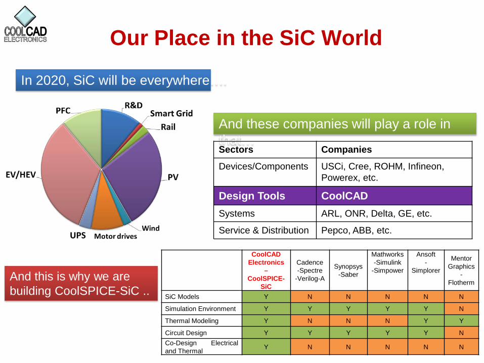
Our Place in the SiC World
CoolCAD Electronics
–CoolSPICE-
SiC
Cadence-Spectre
-Verilog-A
Synopsys-Saber
Mathworks-Simulink
-Simpower
Ansoft-
Simplorer
Mentor Graphics
-Flotherm
SiC Models Y N N N N N
Simulation Environment Y Y Y Y Y N
Thermal Modeling Y N N N Y Y
Circuit Design Y Y Y Y Y NCo-Design Electricaland Thermal Y N N N N N
And this is why we are building CoolSPICE-SiC ..
In 2020, SiC will be everywhere….
And these companies will play a role in that…Sectors Companies
Devices/Components USCi, Cree, ROHM, Infineon, Powerex, etc.
Design Tools CoolCADSystems ARL, ONR, Delta, GE, etc.
Service & Distribution Pepco, ABB, etc.
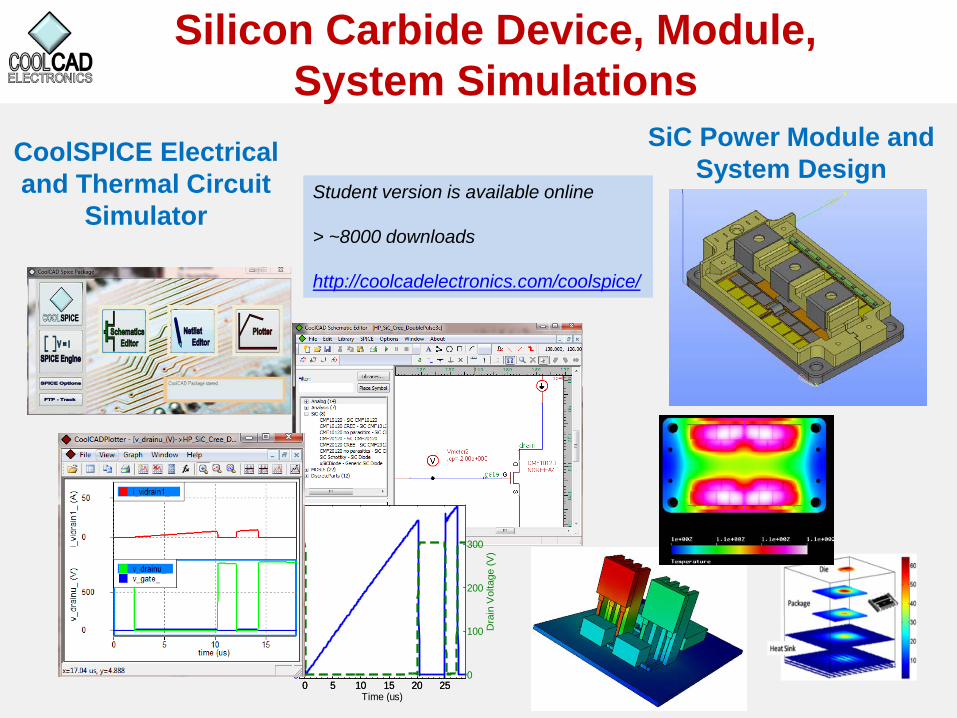
Silicon Carbide Device, Module, System Simulations
CoolSPICE Electrical and Thermal Circuit
Simulator
SiC Power Module and System Design
Student version is available online
> ~8000 downloads
http://coolcadelectronics.com/coolspice/
0 5 10 15 20 250
5
10
15
Dra
in C
urre
nt (A
)
0 5 10 15 20 250
100
200
300
Time (us)
Dra
in V
olta
ge (V
)
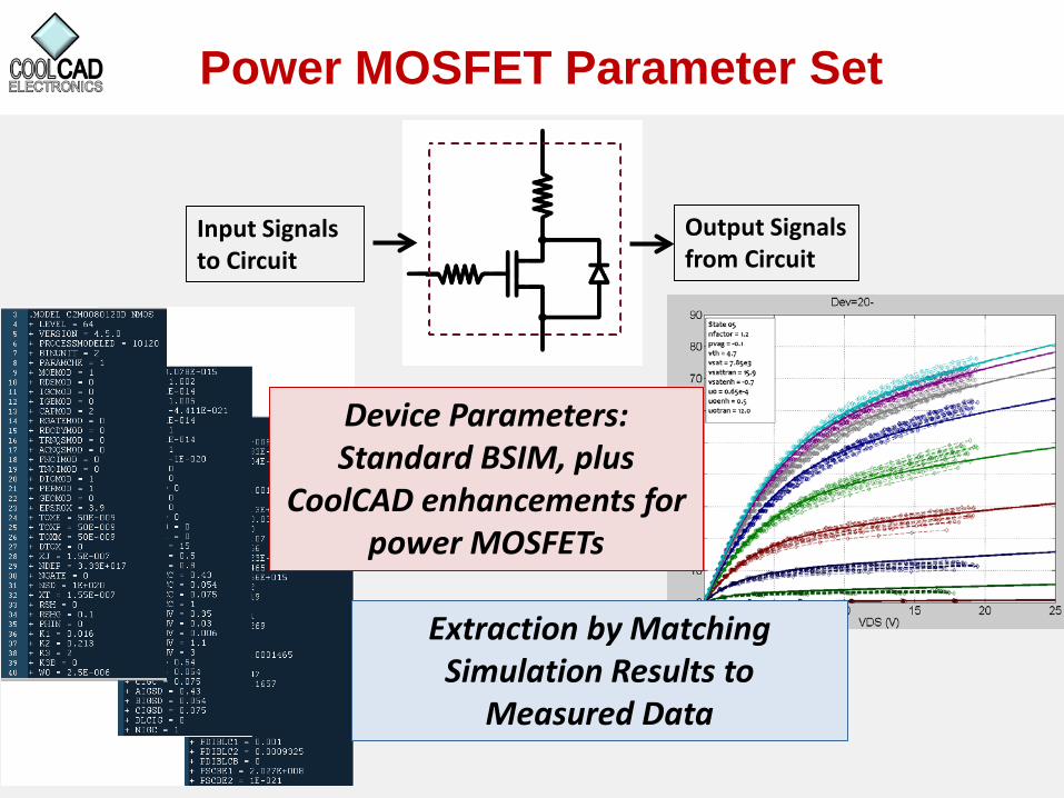
Power MOSFET Parameter Set
Output Signalsfrom Circuit
Input Signalsto Circuit
Extraction by Matching Simulation Results to
Measured Data
Device Parameters:Standard BSIM, plus
CoolCAD enhancements for power MOSFETs
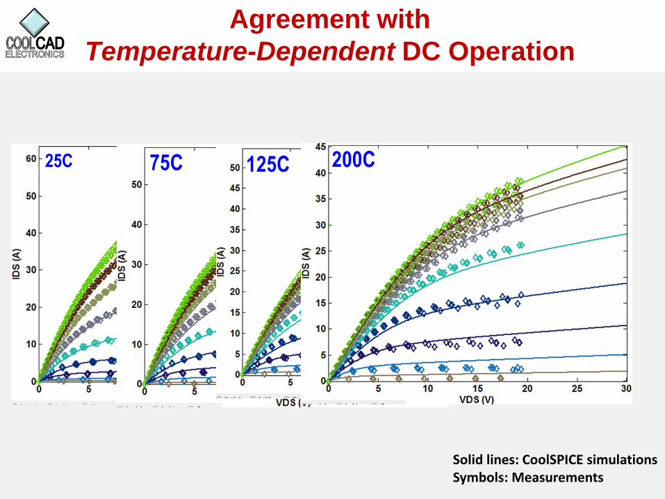
Agreement with Temperature-Dependent DC Operation
Solid lines: CoolSPICE simulationsSymbols: Measurements
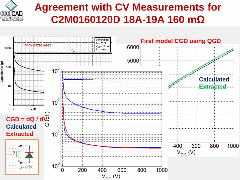
Agreement with CV Measurements forC2M0160120D 18A-19A 160 mΩ
First model CGD using QGD
CalculatedExtracted
CGD = dQ / dVCalculatedExtracted
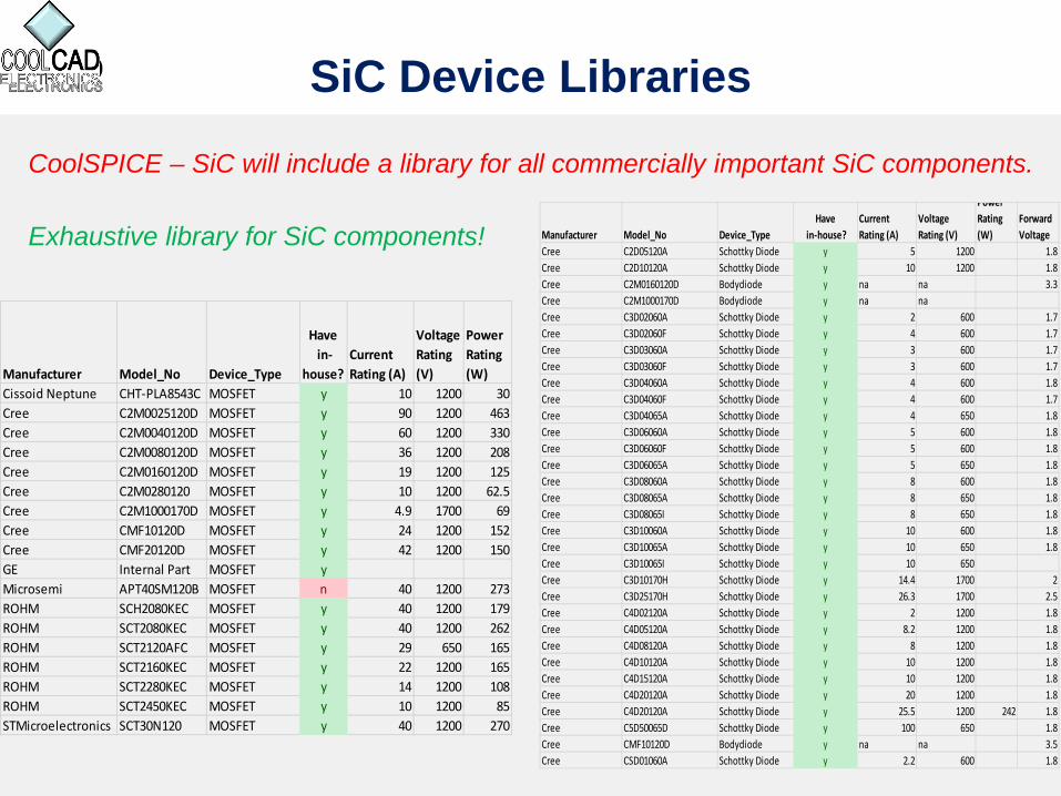
SiC Device Libraries
Manufacturer Model_No Device_Type
Have in-
house?Current Rating (A)
Voltage Rating (V)
Power Rating (W)
Cissoid Neptune CHT-PLA8543C MOSFET y 10 1200 30Cree C2M0025120D MOSFET y 90 1200 463Cree C2M0040120D MOSFET y 60 1200 330Cree C2M0080120D MOSFET y 36 1200 208Cree C2M0160120D MOSFET y 19 1200 125Cree C2M0280120 MOSFET y 10 1200 62.5Cree C2M1000170D MOSFET y 4.9 1700 69Cree CMF10120D MOSFET y 24 1200 152Cree CMF20120D MOSFET y 42 1200 150GE Internal Part MOSFET yMicrosemi APT40SM120B MOSFET n 40 1200 273ROHM SCH2080KEC MOSFET y 40 1200 179ROHM SCT2080KEC MOSFET y 40 1200 262ROHM SCT2120AFC MOSFET y 29 650 165ROHM SCT2160KEC MOSFET y 22 1200 165ROHM SCT2280KEC MOSFET y 14 1200 108ROHM SCT2450KEC MOSFET y 10 1200 85STMicroelectronics SCT30N120 MOSFET y 40 1200 270
Manufacturer Model_No Device_TypeHave
in-house?Current Rating (A)
Voltage Rating (V)
Power Rating (W)
Forward Voltage
Cree C2D05120A Schottky Diode y 5 1200 1.8Cree C2D10120A Schottky Diode y 10 1200 1.8Cree C2M0160120D Bodydiode y na na 3.3Cree C2M1000170D Bodydiode y na naCree C3D02060A Schottky Diode y 2 600 1.7Cree C3D02060F Schottky Diode y 4 600 1.7Cree C3D03060A Schottky Diode y 3 600 1.7Cree C3D03060F Schottky Diode y 3 600 1.7Cree C3D04060A Schottky Diode y 4 600 1.8Cree C3D04060F Schottky Diode y 4 600 1.7Cree C3D04065A Schottky Diode y 4 650 1.8Cree C3D06060A Schottky Diode y 5 600 1.8Cree C3D06060F Schottky Diode y 5 600 1.8Cree C3D06065A Schottky Diode y 5 650 1.8Cree C3D08060A Schottky Diode y 8 600 1.8Cree C3D08065A Schottky Diode y 8 650 1.8Cree C3D08065I Schottky Diode y 8 650 1.8Cree C3D10060A Schottky Diode y 10 600 1.8Cree C3D10065A Schottky Diode y 10 650 1.8Cree C3D10065I Schottky Diode y 10 650Cree C3D10170H Schottky Diode y 14.4 1700 2Cree C3D25170H Schottky Diode y 26.3 1700 2.5Cree C4D02120A Schottky Diode y 2 1200 1.8Cree C4D05120A Schottky Diode y 8.2 1200 1.8Cree C4D08120A Schottky Diode y 8 1200 1.8Cree C4D10120A Schottky Diode y 10 1200 1.8Cree C4D15120A Schottky Diode y 10 1200 1.8Cree C4D20120A Schottky Diode y 20 1200 1.8Cree C4D20120A Schottky Diode y 25.5 1200 242 1.8Cree C5D50065D Schottky Diode y 100 650 1.8Cree CMF10120D Bodydiode y na na 3.5Cree CSD01060A Schottky Diode y 2.2 600 1.8
CoolSPICE – SiC will include a library for all commercially important SiC components.
Exhaustive library for SiC components!
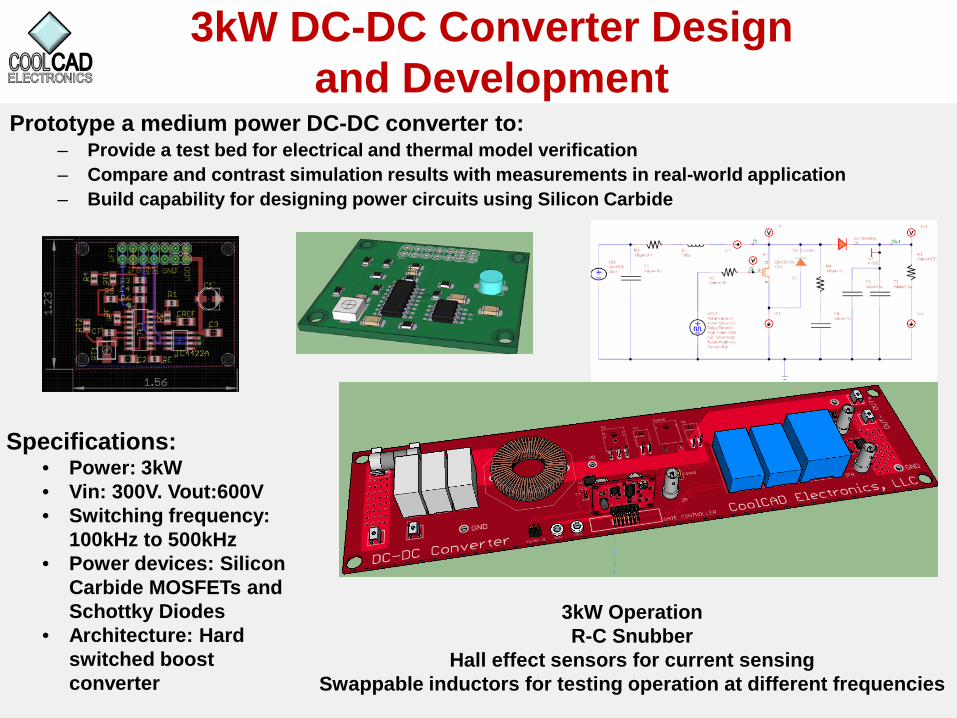
3kW DC-DC Converter Design and Development
Prototype a medium power DC-DC converter to:– Provide a test bed for electrical and thermal model verification– Compare and contrast simulation results with measurements in real-world application– Build capability for designing power circuits using Silicon Carbide
Specifications:• Power: 3kW• Vin: 300V. Vout:600V• Switching frequency:
100kHz to 500kHz• Power devices: Silicon
Carbide MOSFETs and Schottky Diodes
• Architecture: Hard switched boost converter
3kW OperationR-C Snubber
Hall effect sensors for current sensingSwappable inductors for testing operation at different frequencies
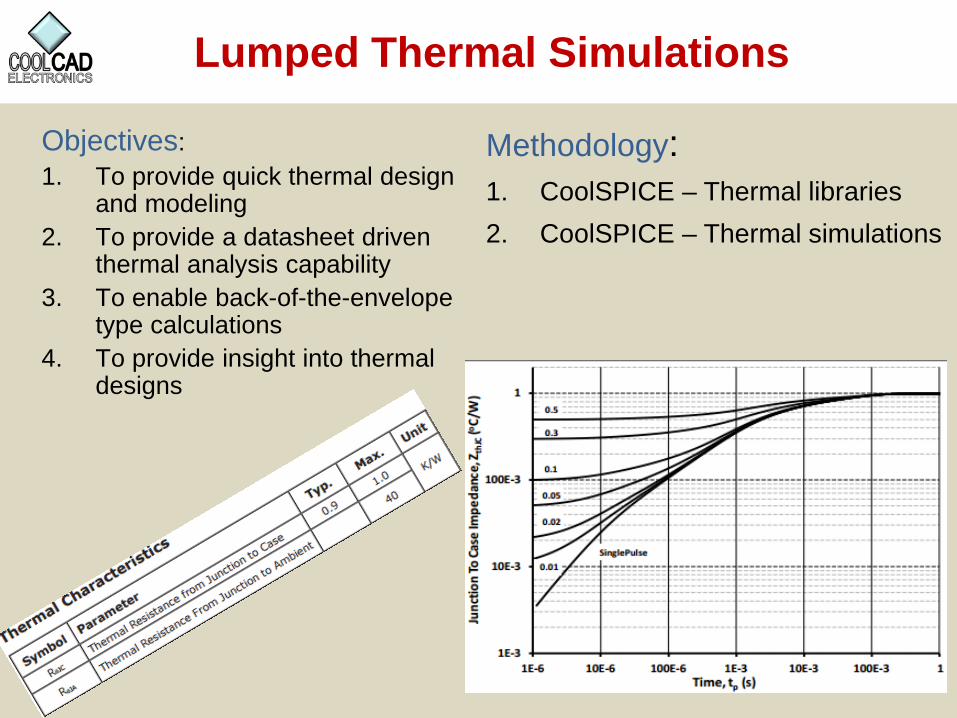
Lumped Thermal Simulations
Objectives: 1. To provide quick thermal design
and modeling2. To provide a datasheet driven
thermal analysis capability3. To enable back-of-the-envelope
type calculations4. To provide insight into thermal
designs
Methodology:1. CoolSPICE – Thermal libraries2. CoolSPICE – Thermal simulations
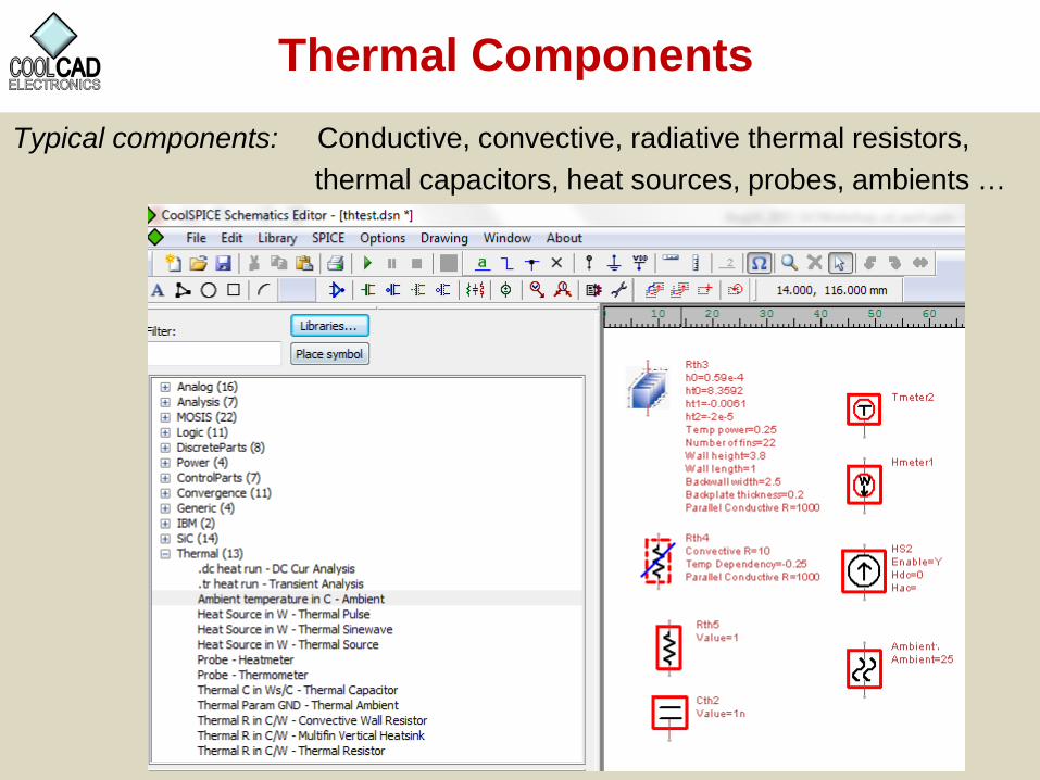
Thermal ComponentsTypical components: Conductive, convective, radiative thermal resistors,
thermal capacitors, heat sources, probes, ambients …
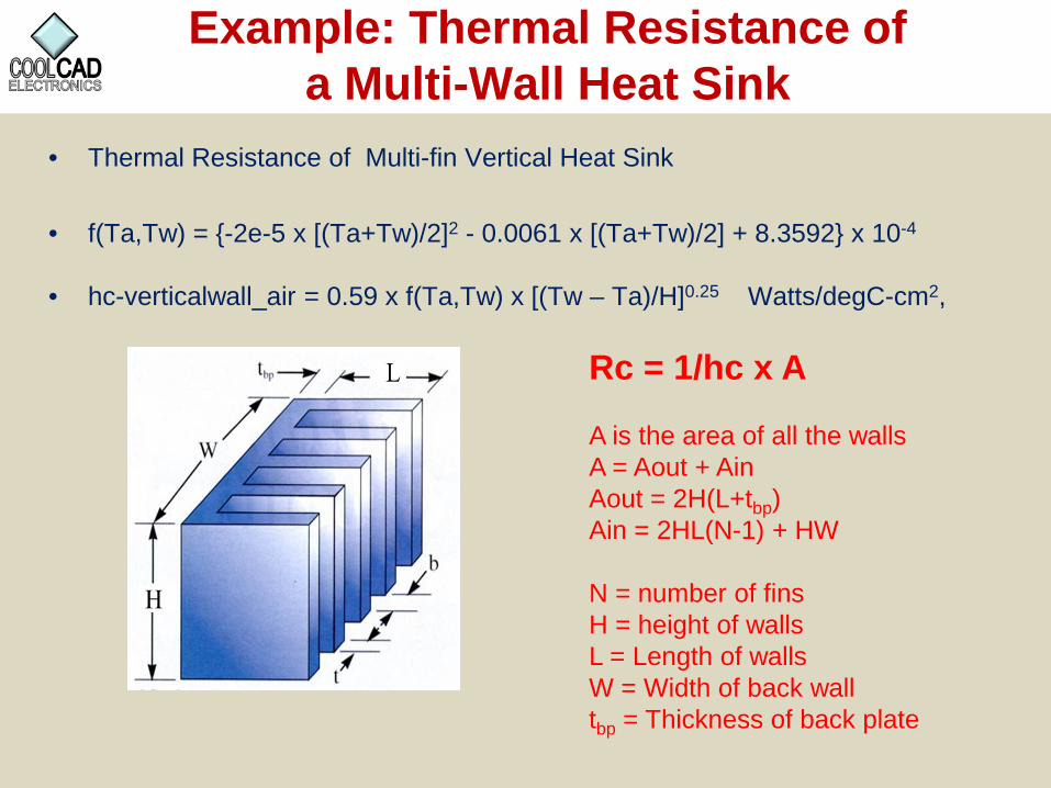
Example: Thermal Resistance of a Multi-Wall Heat Sink
• Thermal Resistance of Multi-fin Vertical Heat Sink
• f(Ta,Tw) = {-2e-5 x [(Ta+Tw)/2]2 - 0.0061 x [(Ta+Tw)/2] + 8.3592} x 10-4
• hc-verticalwall_air = 0.59 x f(Ta,Tw) x [(Tw – Ta)/H]0.25 Watts/degC-cm2,
Rc = 1/hc x A
A is the area of all the wallsA = Aout + AinAout = 2H(L+tbp)Ain = 2HL(N-1) + HW
N = number of finsH = height of wallsL = Length of wallsW = Width of back walltbp = Thickness of back plate
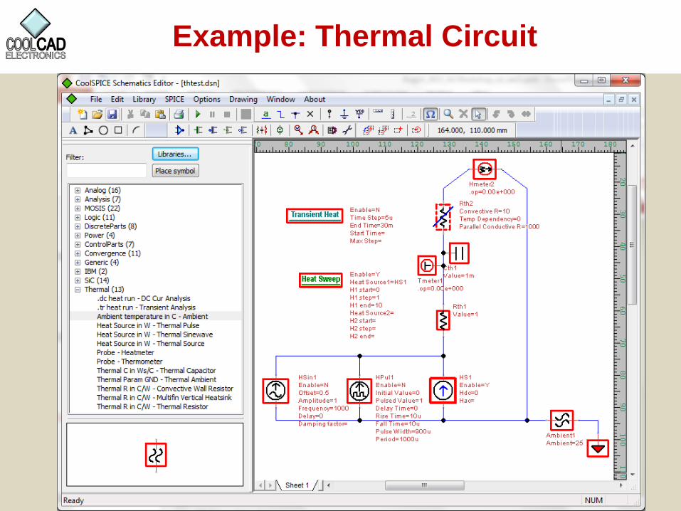
Example: Thermal Circuit
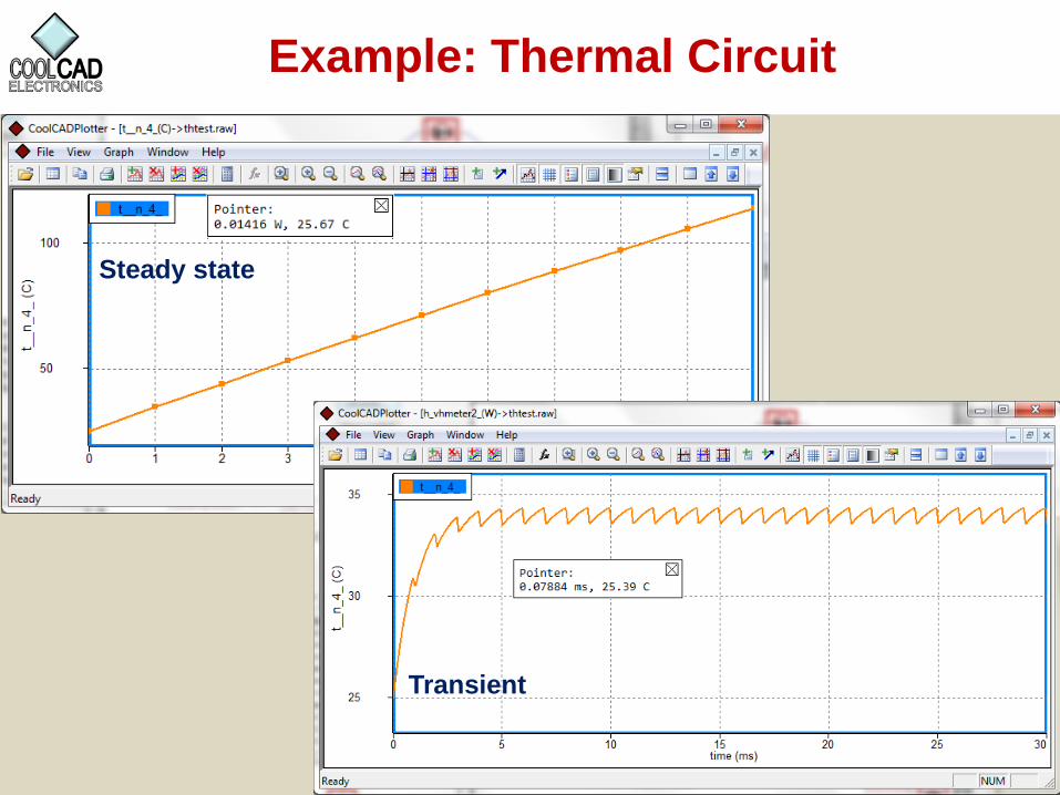
Example: Thermal Circuit
Steady state
Transient
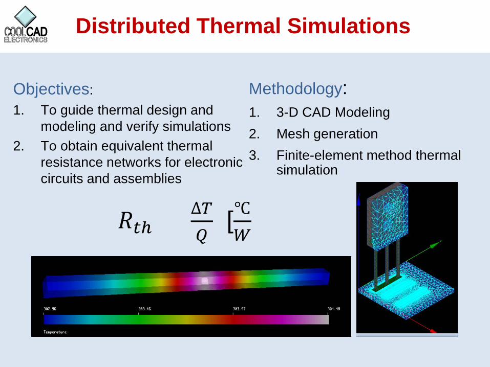
Distributed Thermal Simulations
Objectives: 1. To guide thermal design and
modeling and verify simulations 2. To obtain equivalent thermal
resistance networks for electronic circuits and assemblies
𝑅𝑅𝑡𝑡𝑡 = ∆𝑇𝑇𝑄𝑄
[℃𝑊𝑊
]
Methodology:1. 3-D CAD Modeling2. Mesh generation3. Finite-element method thermal
simulation
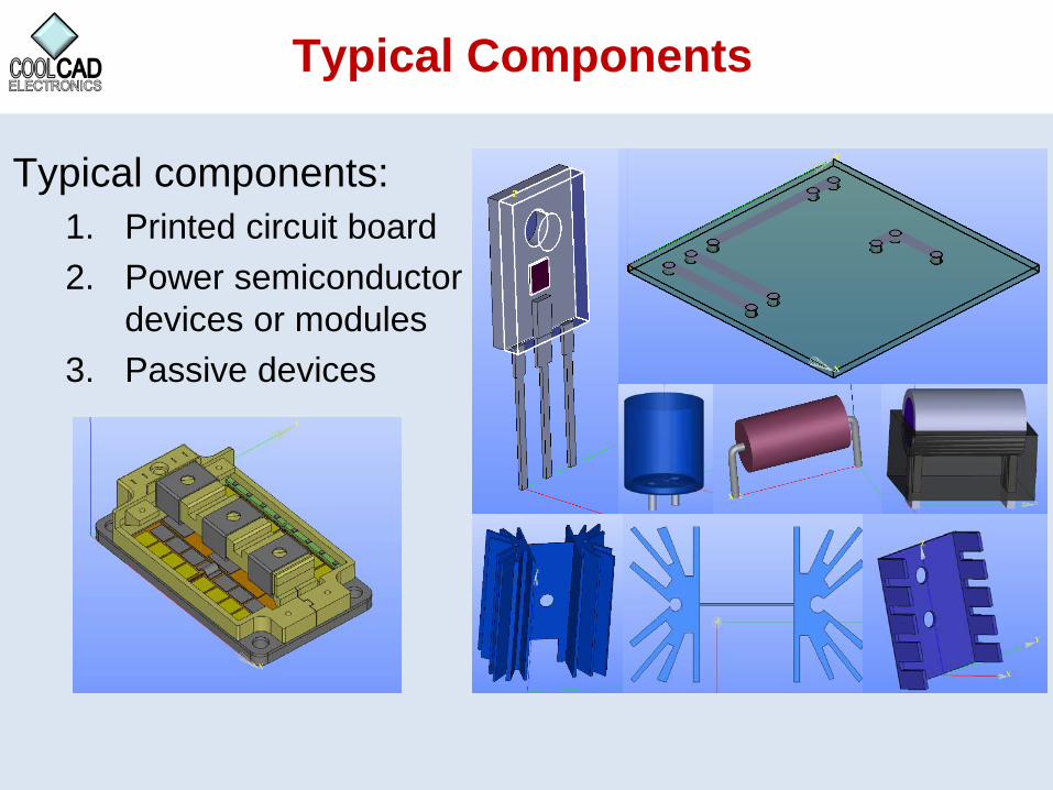
Typical Components
Typical components:1. Printed circuit board 2. Power semiconductor
devices or modules3. Passive devices
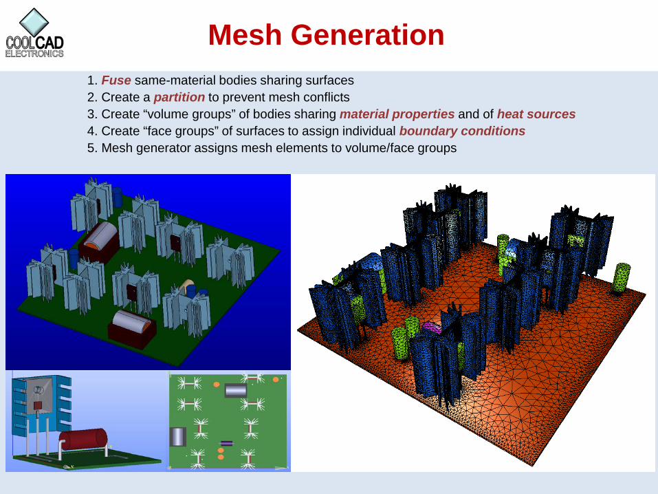
Mesh Generation1. Fuse same-material bodies sharing surfaces2. Create a partition to prevent mesh conflicts 3. Create “volume groups” of bodies sharing material properties and of heat sources4. Create “face groups” of surfaces to assign individual boundary conditions5. Mesh generator assigns mesh elements to volume/face groups
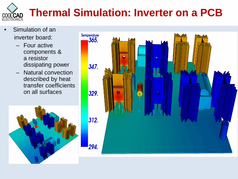
Thermal Simulation: Inverter on a PCB• Simulation of an
inverter board:– Four active
components & a resistor dissipating power
– Natural convection described by heat transfer coefficients on all surfaces
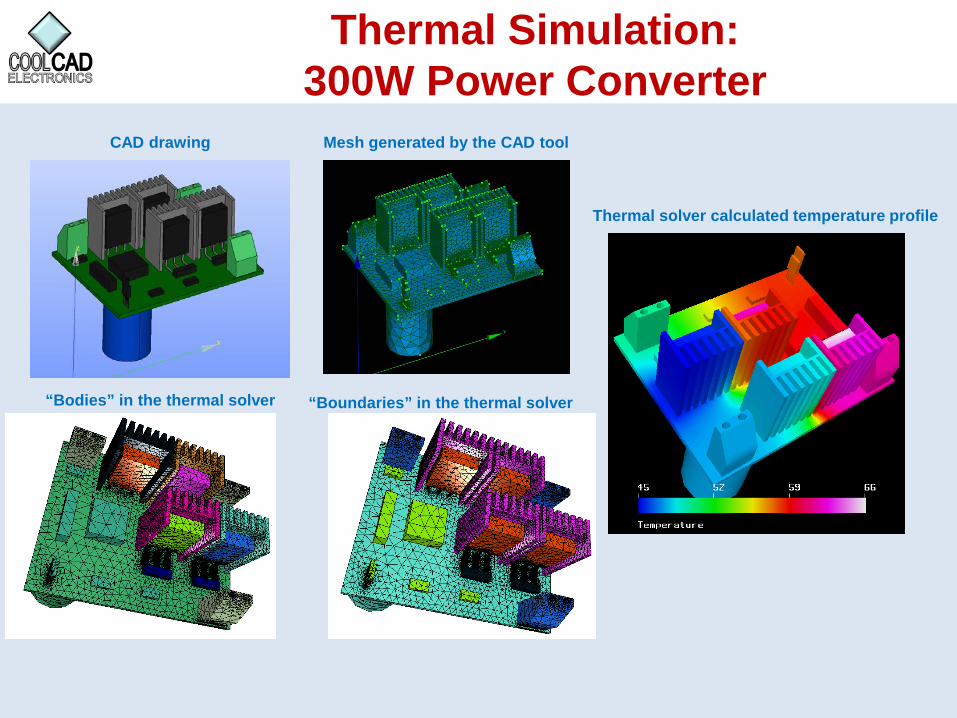
Thermal Simulation: 300W Power Converter
CAD drawing Mesh generated by the CAD tool
“Bodies” in the thermal solver “Boundaries” in the thermal solver
Thermal solver calculated temperature profile
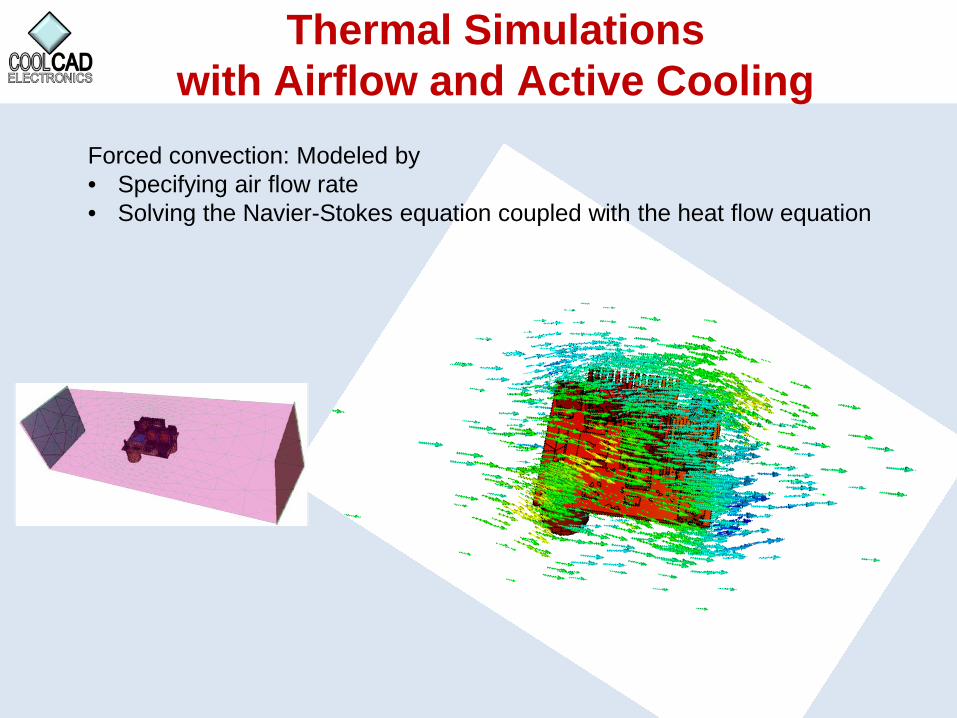
Thermal Simulations with Airflow and Active Cooling
Forced convection: Modeled by • Specifying air flow rate• Solving the Navier-Stokes equation coupled with the heat flow equation

Thermal Simulation: Silicon Carbide Power Module
Module design is from: D. Urciuoli, R. Wood, T. Salem, and G. Ovrebo, “Design and Development of a 400 A, All Silicon-Carbide Power Module” RDECOM presentation
Drawn and meshed in-house at CoolCAD:
12 Diodes16 MOSFETs291000 Nodes1236000 Volume Elements

Thermal Simulation:Silicon Carbide Power Module
CoolCAD calculations: Same geometry, different ambient conditions
TOP:Temperature rise above ambient with aggressive cooling. All dies consume 75W.BOTTOM: Temperature rise above ambient with moderate cooling. MOS dies consume
125W, diodes 75W.
Simulation result from: D. Urciuoli, R. Wood, T. Salem, and G. Ovrebo, “Design
and Development of a 400 A, All Silicon-Carbide Power Module” RDECOM
presentation
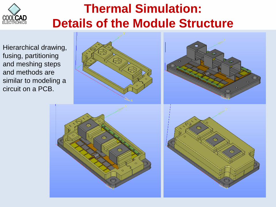
Thermal Simulation:Details of the Module Structure
Hierarchical drawing, fusing, partitioning and meshing steps and methods are similar to modeling a circuit on a PCB.

Brief Explanation of Neutron Effects in SiC Power MOSFETs
Earth Radii
Trapped Proton Belt
4
ABB report on “Failure Rates of HiPak Modules Due to Cosmic Rays”
High energy neutron flux as a function of altitude.

High Energy Neutrons Create High EnergyKnock-On Atoms in SiC Devices
Knock-on atoms in SiC due to atmospheric neutrons
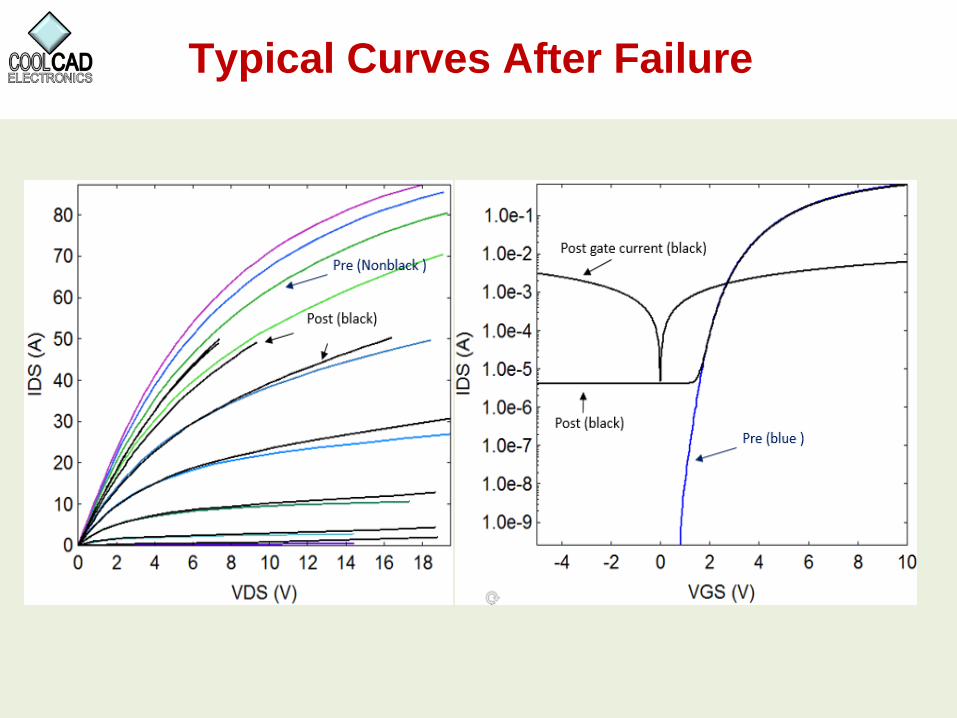
Typical Curves After Failure
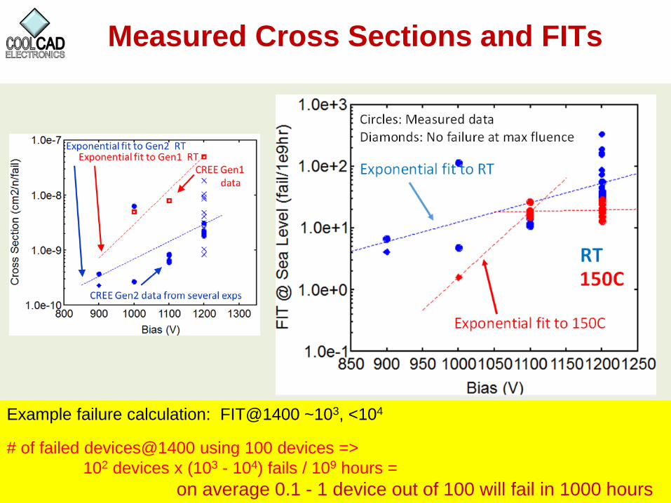
Measured Cross Sections and FITs
Example failure calculation: FIT@1400 ~103, <104
# of failed devices@1400 using 100 devices => 102 devices x (103 - 104) fails / 109 hours =
on average 0.1 - 1 device out of 100 will fail in 1000 hours
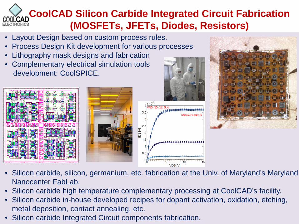
CoolCAD Silicon Carbide Integrated Circuit Fabrication (MOSFETs, JFETs, Diodes, Resistors)
• Layout Design based on custom process rules.• Process Design Kit development for various processes• Lithography mask designs and fabrication• Complementary electrical simulation tools
development: CoolSPICE.
• Silicon carbide, silicon, germanium, etc. fabrication at the Univ. of Maryland’s Maryland Nanocenter FabLab.
• Silicon carbide high temperature complementary processing at CoolCAD’s facility.• Silicon carbide in-house developed recipes for dopant activation, oxidation, etching,
metal deposition, contact annealing, etc.• Silicon carbide Integrated Circuit components fabrication.
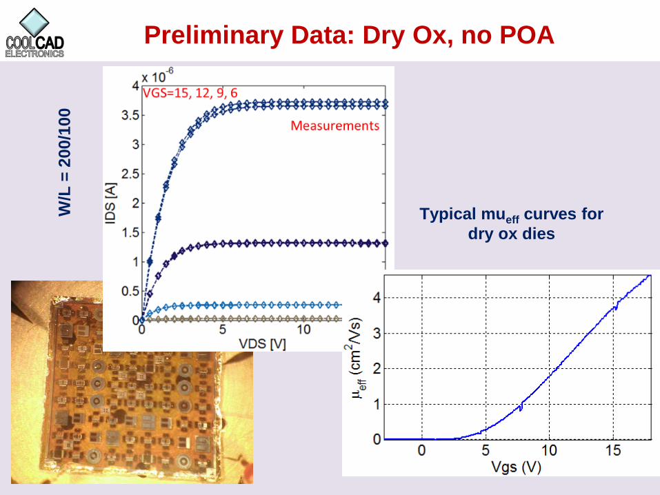
Preliminary Data: Dry Ox, no POA W
/L =
200
/100
Typical mueff curves for dry ox dies
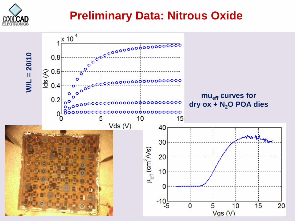
Preliminary Data: Nitrous OxideW
/L =
20/
10
mueff curves for dry ox + N2O POA dies
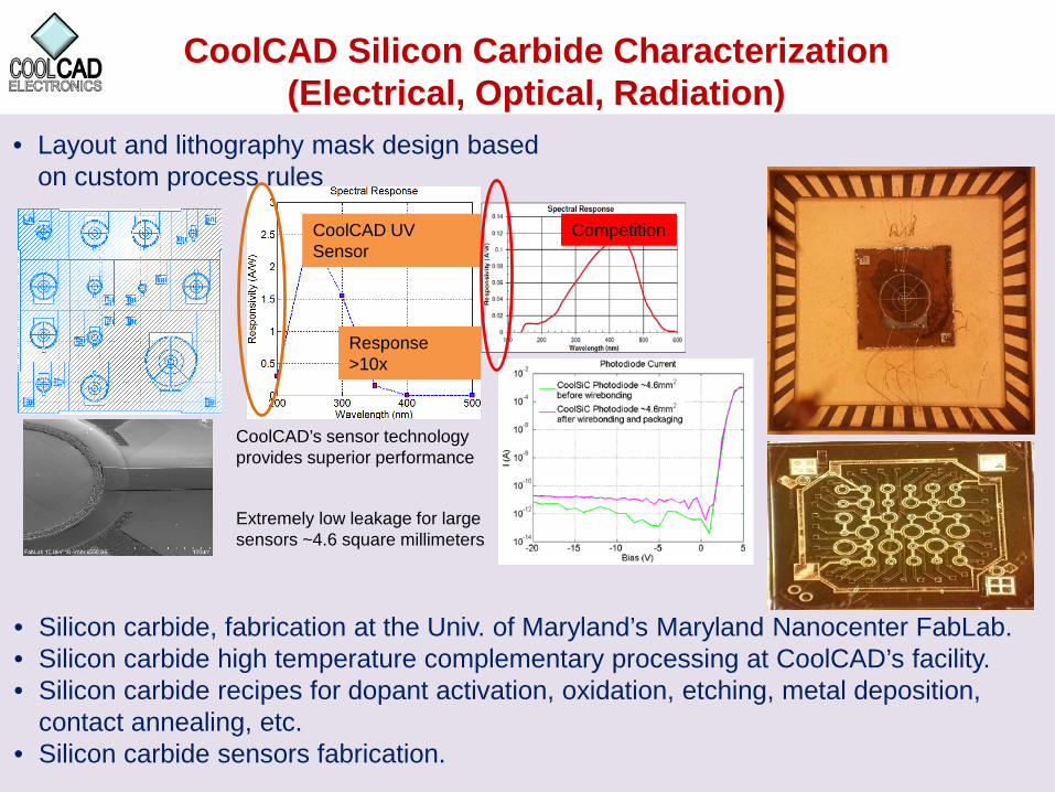
CoolCAD Silicon Carbide Characterization(Electrical, Optical, Radiation)
• Layout and lithography mask design based on custom process rules
• Silicon carbide, fabrication at the Univ. of Maryland’s Maryland Nanocenter FabLab.• Silicon carbide high temperature complementary processing at CoolCAD’s facility.• Silicon carbide recipes for dopant activation, oxidation, etching, metal deposition,
contact annealing, etc.• Silicon carbide sensors fabrication.
Extremely low leakage for large sensors ~4.6 square millimeters
CoolCAD UV Sensor
Competition
Response >10x
CoolCAD’s sensor technology provides superior performance