Embed Size (px)
Citation preview

ELECTRICAL ENGINEERING SOLVERPACK PART 1 OF 2
Wye-Delta Transformations
Filename: WDT.TK
Useful for: Section 20, Motors. Also (for Wheatstone Bridge, which can be thought of as two deltas): Section 2, page 7; Section 3, pages 43 and 74; Section 16, page 75.
Given a Wye or a Delta circuit, this model will compute the impedances of the other equivalent load.
FIG. 1
Variables St Input Name Output Unit Comment WYE DELTA TRANSFORMATIONS: WDT Impedances of a Wye circuit: Z1 33.333333 Ohm Z 1 (real part) jZ1 0 Ohm Z 1 (imaginary part) Z2 50 Ohm Z 2 (real part)

jZ2 0 Ohm Z 2 (imaginary part) Z3 100 Ohm Z 3 (real part) jZ3 0 Ohm Z 3 (imaginary part) Impedances of a Delta circuit: 100 Za Ohm Z a (real part) jZa 0 Ohm Z a (imaginary part) 200 Zb Ohm Z b (real part) jZb 0 Ohm Z b (imaginary part) 300 Zc Ohm Z c (real part) jZc 0 Ohm> Z c (imaginary part) * If dealing with a resistance, you may leave input imaginary part blank
Rules S Rule " WYE DELTA TRANSFORMATIONS: WDT * if given('Za) then jZa = given('jZa,jZa,0) * if given('Zb) then jZb = given('jZb,jZb,0) * if given('Zc) then jZc = given('jZc,jZc,0) * if given('Z1) then jZ1 = given('jZ1,jZ1,0) * if given('Z2) then jZ2 = given('jZ2,jZ2,0) * if given('Z3) then jZ3 = given('jZ3,jZ3,0) * ((Za,jZa)-(Z1,jZ1)-(Z2,jZ2))*(Z3,jZ3) = (Z1,jZ1)*(Z2,jZ2) * (Z1,jZ1)*((Za,jZa)+(Zb,jZb)+(Zc,jZc)) = (Za,jZa)*(Zb,jZb) * (Za,jZa)/(Zb,jZb) = (Z2,jZ2)/(Z3,jZ3) * (Zb,jZb)/(Zc,jZc) = (Z1,jZ1)/(Z2,jZ2)
Microstrip Calculations
Filename: MSC.TK
Useful for: Section 16, Power System Interconnections, and Section 26, Telecommunications. Also, Section 2, Circuits.
A microstrip (Figure 2) is a low-loss transmission line commonly used in microwave circuits. This model calculates values for the width of the microstrip and the line's velocity factor. At the same time, it calculates the design of strip lines with two ground planes.
In simplest terms, a microstrip is a metal strip supported above a conducting groundplane (or between two of them). Attenuation is higher than for hollow-pipe waveguides, but microstrips tend to be cheaper and more compact. Careful planning of dimensions can minimize problems.

FIG. 2
Variables St Input Name Output Unit Comment MICRO STRIP CALCULATIONS: MSC 70 line Ohm Line impedance 05 subs in Substrate thickness .001 thick in Conductor thickness 4.7 diel Dielectric constant width .04989932 in Microstrip width vlfc .58696727 Velocity factor swidth .0081676 in Strip-line width svlfc .4612656 Velocity factor
Rules S Rule " MICRO STRIP CALCULATIONS: MSC " Formulas for microstrip design: * temp = exp(line*sqrt(diel+1.41)/87) * width = 1.25*(5.98*subs/temp-thick) * vlfc = 1/sqrt(0.475*diel+.67) " Formulas for strip-line design: * stemp = exp(line*sqrt(diel)/60) * swidth = .59*(4*subs/stemp-2.1*thick) * svlfc = 1/sqrt(diel)
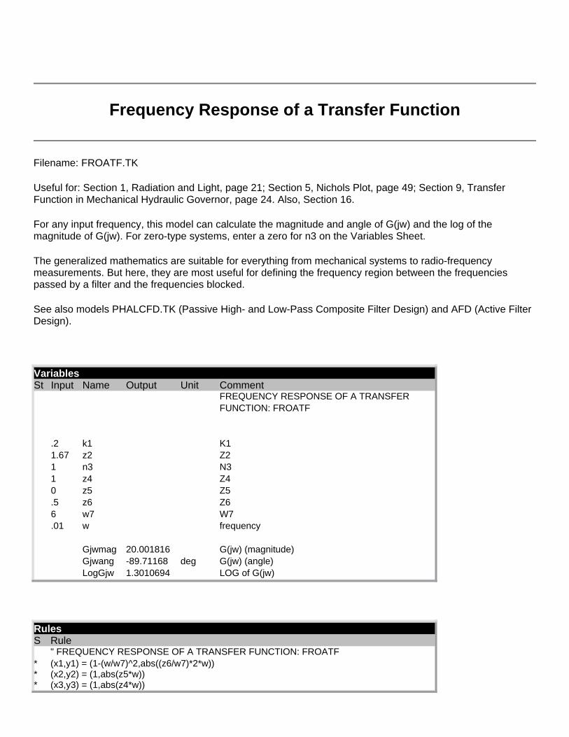
Frequency Response of a Transfer Function
Filename: FROATF.TK
Useful for: Section 1, Radiation and Light, page 21; Section 5, Nichols Plot, page 49; Section 9, Transfer Function in Mechanical Hydraulic Governor, page 24. Also, Section 16.
For any input frequency, this model can calculate the magnitude and angle of G(jw) and the log of the magnitude of G(jw). For zero-type systems, enter a zero for n3 on the Variables Sheet.
The generalized mathematics are suitable for everything from mechanical systems to radio-frequency measurements. But here, they are most useful for defining the frequency region between the frequencies passed by a filter and the frequencies blocked.
See also models PHALCFD.TK (Passive High- and Low-Pass Composite Filter Design) and AFD (Active Filter Design).
Variables St Input Name Output Unit Comment FREQUENCY RESPONSE OF A TRANSFER FUNCTION: FROATF .2 k1 K1 1.67 z2 Z2 1 n3 N3 1 z4 Z4 0 z5 Z5 .5 z6 Z6 6 w7 W7 .01 w frequency Gjwmag 20.001816 G(jw) (magnitude) Gjwang -89.71168 deg G(jw) (angle) LogGjw 1.3010694 LOG of G(jw)
Rules S Rule " FREQUENCY RESPONSE OF A TRANSFER FUNCTION: FROATF * (x1,y1) = (1-(w/w7)^2,abs((z6/w7)*2*w)) * (x2,y2) = (1,abs(z5*w)) * (x3,y3) = (1,abs(z4*w))

* (x5,y5) = (k1,abs(z2*w*k1)) * (Gjwx,Gjwy) = (x5,y5)/((x1,y1)*(x2,y2)*(x3,y3)*ptord(w^n3,n3*90)) * (Gjwmag,Gjwang) = rtopd(Gjwx,Gjwy) * LogGjw = log(Gjwmag)
Transistor Amplifier Performance
Filename: TAP.TK
Useful for: Section 13, Power Electronics; Section 2, Electric and Magnetic Circuits
Given the magnitude and angle of the H-parameter matrix (Figure 3) and source and load impedances, this model calculates voltage gain, current gain, input impedance, and output impedance.
With the matrix notation, the answers are independent of transistor type, for "small" signal strengths. In a sense, the transistor amplifier part of the circuit becomes a black box.
The model's notation are the following:
hi = small-signal input impedance with output AC short-circuited. hr = small-signal reverse voltage transfer ratio with input AC open-circuited. hf = small-signal current gain, output AC short-circuited. ho = small-signal output admittance with input AC open-circuited.
Note:
This notation is not used in the book itself. See Modern Electronic Circuit Design, also published by McGraw-Hill, for a more complete discussion.
FIG. 3

Variables St Input Name Output Unit Comment TRANSISTOR AMPLIFER PERFORMANCE: TAP 1100 himag hi of h-parameter matrix (magnitude) 0 hiang deg hi of h-parameter matrix (angle) .00025 hrmag hr of h-parameter matrix (magnitude) 0 hrang deg hr of h-parameter matrix (angle) 50 hfmag hf of h-parameter matrix (magnitude) 0 hfang deg hf of h-parameter matrix (angle) .000025 homag ho of h-parameter matrix (magnitude) 0 hoang deg ho of h-parameter matrix (angle) 1000 rs Ohm source impedance (magnitude) 0 os deg source impedance (angle) 10000 rl Ohm load impedance (magnitude) 0 ol deg load impedance (angle) Avmag -400 Voltage gain (magnitude) Avang 0 deg Voltage gain (angle) Aimag -40 Current gain (magnitude) Aiang 0 deg Current gain (angle) Avsmag -200 Voltage gain with source resistor(mag) Avsang 0 deg Voltage gain with source resistor(ang) Zinmag 1000 Input impedance (magnitude) Zinang 0 deg Input impedance (angle) Zoutmag 52500 Output impedance (magnitude) Zoutang 0 deg Output impedance (angle)
Rules S Rule " TRANSISTOR AMPLIFIER PERFORMANCE: TAP * (x1,y1) = ptord(homag,hoang)*ptord(rl,ol) * (Aix,Aiy) = ptord(hfmag,hfang)/((x1+1),y1)

* (Aimgg,Aiang) = rtopd(Aix,Aiy) * Aimag = -Aimgg * (x21,y21) = ptord(himag,hiang) * x22 = Aimag*rl*hrmag*cosd(Aiang+ol+hrang) * y22 = Aimag*rl*hrmag*sind(Aiang+ol+hrang) * (mag23,ang23) = rtopd((x21+x22),(y21+y22)) * Zinmag = mag23 * Zinang = ang23 * (x31,y31) = ptord(rs,os) * (x32,y32) = ptord(Zinmag,Zinang) * (mag33,ang33) = rtopd((x31+x32),(y31+y32)) * Avsmag = rl*Aimag/mag33 * Avsang = ol + Aiang - ang33 * (x41,y41) = ptord(rs,os) * (x42,y42) = ptord(himag,hiang) * (mag43,ang43) = rtopd((x41+x42),(y41+y42)) * x51 = homag*cosd(hoang) * y51 = homag*sind(os) * tempz = -hrmag*hfmag/mag43 * tempt = hrang + hfang - ang43 * (x52,y52) = ptord(tempz,tempt) * (mag53,ang53) = rtopd((x51+x52),(y51+y52)) * Zoutmag = 1/mag53 * Zoutang = -ang53 * Avmag = Aimag*rl/Zinmag * Avang = Aiang + ol - ang23
Unilateral Design
Filename: UD.TK
Useful for: Section 10, especially pages 98 and following; Section 28, especially page 8 and following
A "unilateral" transducer device is one in which the reverse-transmission factor (s12 in the model's notation) can be safely neglected. If s12 can be neglected (if it is close to zero or at least small compared with the other s factors), the model will compute values for maximum and minimum gain (Gmin, Gmax, etc.) distance from origin, and radius of circle.
In the example, s12 is .09, while other s values are s11 = .51; s21 = 1.4; s22 = .6 (see first group of variables on the Variables Sheet).
Gmax is the power delivered to load, divided by power available from the source if, indeed, s12 can be ignored.
In the model's notation, G1max is the gain contribution from change of source impedance from zo to s11, and so forth.
Warning: If U is not small (it is 0.08142148 in the example), Gmax will be overestimated.

These are the formulas used in this model. Notice that the s factors are complex quantities. Since only their magnitude is required in the formulas, this angle is not needed as an input.
u = |s11s12s21s22| / |[(1 - |s11|2)(1 - |s22|2)]|
Clearly the unilateral assumption is more nearly correct for u near zero.
The maximum unilateral transducer power gain is given by:
Gu = (Power delivered to load) / (Power available from source) |s21|2 / |[(1 - |s11|2)(1 - |s22|2)]|
Using the unilateral figure of merit, we can place limits on the actual transducer power gain:
Gmin = Gu[1 / (1+u)2] Gmax = Gu[1 / (1-u)2]
When input and output impedances are conjugately matched, the transducer power gain is:
Gu = G0 · G1 · G2 Where Gu = transducer power gain
= (power delivered to load) / (power available from source) G0 = |s21|2 = transducer gain for Z0 input and
output impedances G1,max = 1 / (1 - |s11|2) = gain contribution from change of source
impedance from Z0 to s11* G2,max = 1 / (1 - |s22|2 = gain contribution from change of load
impedance from Z0 to s22* sij* = complex conjugate of sij
from the origin.
The radius of the circle is
0i = {sqrt[1 - Gi(1 - |sii|2)] / [1 + Gi|sii|2]} r0i = (Gisii) / (1 + Gi|sii|2)
Variables St Input Name Output Unit Comment UNILATERAL DESIGN - MERIT, GAIN & CIRCLES: UD .51 s11 Transistor S[1,1] parameter magnitude .09 s12 Transistor S[1,2] parameter magnitude 1.4 s21 Transistor S[2,1] parameter magnitude .6 s22 Transistor S[2,2] parameter magnitude .5 g1 db G1 {to calculate Ro1 & Po1} .5 g2 db G2 {to calculate Ro2 & Po2} U .08142148 Unilateral figure of merit Gu 6.1690307 Transducer power gain Gmin 5.4891309 Minimum transducer power gain

Gmax 6.9067049 Maximum transducer power gain G0 2.9225607 Transducer gain for Z0 input & output G1max 1.3082697 Delta gain fr. change fr. Z0 to S[1,1] G2max 1.9382003 Delta gain fr. change fr. Z0 to S[2,2] Ro1 .44295791 ro1 dist. from the origin(input plane) Po1 .31899571 po1 radius of the circle(input plane) Ro2 .47952012 ro2 dist. fr. the origin(output plane) Po2 .37818947 po2 radius of the circle(output plane)
Rules S Rule " UNILATERAL DESIGN - MERIT, GAIN & CIRCLES: UD * U = abs(s11*s12*s21*s22/((1-s11^2)*(1-s22^2))) * Gutemp = s21^2/abs((1-s11^2)*(1-s22^2)) * Gu = log(Gutemp)*10 * Gmin = log(Gutemp/(1+U)^2)*10 * Gmax = log(Gutemp/(1-U)^2)*10 * G0 = log(s21^2)*10 * G1max = log(1/(1-s11^2))*10 * G2max = log(1/(1-s22^2))*10 * G1temp = 10^(g1/10) * G2temp = 10^(g2/10) * Ro1 = G1temp*s11/(1+G1temp*s11^2) * Po1 = sqrt(1-G1temp*(1-s11^2))/(1+G1temp*s11^2) * Ro2 = (G2temp*s22)/(1+G2temp*s22^2) * Po2 = sqrt(1-G2temp*(1-s22^2))/(1+G2temp*s22^2)
Bilateral Design
Filename: BD.TK
Useful for: Section 10, especially page 98 and following; Section 28, especially page 8 and following
A "bilateral" transducer device is one in which the reverse-transmission factor (s12 in the model's notation) cannot be ignored. If s12 cannot be neglected (if it is not close to zero, or it is large compared to the other s factors), the model will compute values for maximum gain (GMAX), stability factor, source reflection coefficient, and load reflection.
In the example, s12mag is .078 and s12ang is 93 degrees, while other s values are comparable in order of magnitude (see first group of variables on the Variables Sheet).
These are the formulas used in this model:
K = (1 + | |2 - |s11|2 - |s22|2) / 2 |s21 s12| Sij are s parameters

Gmax = [|s21| / |s12|] [K sqrt(K2 - 1)]
in which the plus sign is used when the quantity
B1 = 1 + |s11|2 - |s22|2 - | |2
is negative and the minus sign is used when B1 is positive.
The second portion of this program computes values of source and load reflection coefficients required to conjugately match the transistor using the equations
ms = {C1*} {[B1 sqrt(B12 - 4|C2|2)] / [2 |C2|2]}
m1 = {C2*} {[B2 sqrt(B22 - 4|C2|2)] / [2 |C2|2]}
where C1 = s11 - s*22 C1* = complex conjugate of C1 C2 = s22 - s*11 C2* = complex conjugate of C2 B1 = 1 + |s11|2- |s22|2 - | |2 B2 = 1 + |s22|2- |s11|2 - | |2
Variables St Input Name Output Unit Comment BILATERAL DESIGN - STABILITY, GAIN & MATCHING: BD .277 s11mag S-Parameter Matrix Item S11 (magn.) -59 s11ang deg S-Parameter Matrix Item S11 (angle) .078 s12mag S-Parameter Matrix Item S12 (magn.) 93 s12ang deg S-Parameter Matrix Item S12 (angle) 1.92 s21mag S-Parameter Matrix Item S21 (magn.) 64 s21ang deg S-Parameter Matrix Item S21 (angle) .848 s22mag S-Parameter Matrix Item S22 (magn.) -31 s22ang deg S-Parameter Matrix Item S22 (angle) K 1.0325237 Stability factor GMAX 12.807406 db Maximum gain Lmsmag .72981167 Source reflection coefficient (magn.) Lmsang 135.4438 deg Source reflection coefficient (angle) Lmlmag .9510996 Load reflection coefficient (magn.)

Lmlang 33.851189 deg Load reflection coefficient (angle)
Rules S Rule " BILATERAL DESIGN - STABILITY, GAIN & MATCHING: BD * (x1,y1) = ptord(1,(s11ang+s22ang)) * (x2,y2) = ptord(1,(s12ang+s21ang)) * x3 = -x2*s12mag*s21mag * y3 = s11mag*s22mag*y1-y2*s12mag*s21mag * (mag3,ang3) = rtopd(x3,y3) * tempd = s11mag^2 - s22mag^2 + 1 - mag3^2 * if tempd = 0 then temp1 = 1 else temp1 = tempd * K = (mag3^2+1-s11mag^2-s22mag^2)/(2*abs(s12mag*s21mag)) * GMAX = log((K-sqrt(K*K-1)*abs(temp1)/tempd)*s21mag/s12mag)*10 * (x4,y4) = ptord(s11mag,s11ang) * ang5 = ang3 - s22ang * mag5 = -s22mag*mag3 * (x5,y5) = ptord(mag5,ang5) * x6 = x4 + x5 * y6 = y4 + y5 * (mag6,ang6) = rtopd(x6,y6) * tempd1 = s11mag^2 - s22mag^2 + 1 - mag3^2 * Lmsmag = tempd1/mag6/2 - sqrt((tempd1/mag6/2)^2-1) * Lmsang = -ang6 * (x7,y7) = ptord(s22mag,s22ang) * ang8 = ang3 - s11ang * mag8 = -s11mag*mag3 * (x8,y8) = ptord(mag8,ang8) * x9 = x7 + x8 * y9 = y7 + y8 * (mag9,ang9) = rtopd(x9,y9) * tempd2 = s22mag^2 - s11mag^2 + 1 - mag3^2 * Lmlmag = tempd2/mag9/2 - sqrt((tempd2/mag9/2)^2-1) * Lmlang = -ang9
Smith Chart Conversions
Filename: SCC.TK
Useful for: Section 16, Microwaves
On a microwave transmission line, if the impedance at any point is known (relative to the line's characteristic impedance), the impedance at any other point can be calculated.
Using this model, you can convert between return loss, reflection coefficient, the voltage standing-wave ratio, and standing-wave ratio. Essentially, the TK Solver automates the nomograph in Figure 4, and allows computation of impedance and reflection coefficients.

The model solves these equations:
Standing-wave ratio (decibels) = 20 log (voltage standing-wave ratio)
Return loss = 20 log * (1 / complex reflection coefficient absolute value)
Voltage standing-wave ratio
= (1 + complex reflection coefficient) / (1 - complex reflection coefficient)
FIG. 4a
FIG. 4b

Variables St Input Name Output Unit Comment SMITH CHART CONVERSIONS: SCC ro 1.9952623 V Voltage standing wave ratio 6 SWR db Standing wave ratio in decibels p .33227885 Reflection coefficient RL 9.569946 db Return loss 50 Z0 Ohm Z0 62 mag Ohm Reflection or impedance magnitude 37 ang deg Reflection or impedance angle RCo .35110567 Reflection coefficient "o" RCp 70.190944 Reflection coefficient "p" IMo 178.88755 Ohm Impedance 0 IMZ 51.304806 Ohm Impedance Z

Rules S Rule " SMITH CHART CONVERSIONS: SCC * ro = 10^(SWR/20) * SWR = 20*LOG(ro) * p = (ro-1)/(ro+1) * ro = (1+p)/(1-p) * RL = 20*LOG(1/p) * p = 10^(-RL/20) " Compute reflection coefficient: * (x,y) = ptord(mag,ang) * (RCx,RCy) = (x-Z0,y)/(x+Z0,y) * (RCo,RCp) = rtopd(RCx,RCy) " Compute the impedance: * (IMtx,IMty) = ((x+1,y)/(x-1,y)) * IMx = -IMtx*Z0 * IMy = -IMty*Z0 * (IMZ,IMo) = rtopd(IMx,IMy)
Class A Transistor Amplifier
Filename: CATA.TK
Useful for: Section 28, Solid State Amplifiers, page 4
This model will calculate the resistor values for a circuit acting as a Class A (low-power, low-efficiency) amplifier. If the range between Iemin and Iemax (minimum and maximum emitter currents) is too narrow for the other variables to be calculated properly, an error message will appear.
Because Class A amplifiers have a low conversion efficiency, they are used mainly in low power applications - loads of 10 watts or less. In fact, the maximum possible efficiency is only 50 percent. This means that the circuit will produce a great deal of heat. So the model calculates base-emitter voltage under hot, high-current conditions and under cold, low-current conditions.
Figure 5 labels components using the same terminology as the model.
FIG. 5

Variables St Input Name Output Unit Comment CLASS A TRANSISTOR AMPLIFIER: CATA 10 tol % Tolerance of resistors 'g type Trans. type ('g = germanium, 's = silicon) -25 tempmin oC Minimum temperature 75 tempmax oC Maximum temperature 50 betamin Minimum beta 150 betamax Maximum beta 12 supvolt V Supply voltage 2000 resist Ohm Emitter resistor value 5 etol % Emitter resistor tolerance 5 Vce Vce .002 Icbo mA Icbo .8 Iemin mA Ie minimum 1.2 Iemax mA Ie maximum R1 47000 Ohm R(betamin) R2 18000 Ohm R(betamax) R3 4700 Ohm R(c) R4 2000 Ohm R(e) BIAS 3.5828523 V Bias voltage
Rules S Rule " CLASS A TRANSISTOR AMPLIFER DESIGN: CATA * I1t = Iemin*(1-.03*etol)

* I2t = Iemax*(1+.03*etol) * betamint = betamin*.865*exp(.00575*tempmin) * t3 = tempmax - 25 * bz = .00895 - .00565*t3 + .00048*t3^2 * betamaxt = betamax*(.865*exp(.00575*tempmax)+(type = 'g)*bz) * temp = Icbo*exp(.075*t3) * if type = 'g then Icbot = temp else Icbot = Icbo * R3t = 2000*(supvolt-Vce)/(I1t+I2t) - resist * bx = betamaxt + 1 * Num = (I2t-I1t)*resist+2.5*(tempmax-tempmin) * Den = Icbot + I2t/(betamint+1) - I1t/bx * r6 = Num/Den * if r6 < = 0 then call errmsg('The,'range,'of,'Ie,'is,'too,'narrow) * t4 = tempmin - 25 * BIAS = I2t*.001*(r6/(betamint+1)+resist) + .2 + .5*(type = 's) - .0025*t4 * R3 = CalcStandard(R3t,tol) * R4 = resist * R1t = supvolt*r6/BIAS * R1 = CalcStandard(R1t,tol) * R2t = supvolt*r6/(supvolt-BIAS) * R2 = CalcStandard(R2t,tol)
RULE FUNCTION: CalcStandard Comment: Calculate standard resistor value Parameter Variables: Argument Variables: Rt,t Result Variables: R S Rule cv = Rt t4 = 1.19927e-2*int(1+1.5*t+.004*t^2) t3 = int(ln(cv)/ln(10)-int(2.2-3*t4)) cvtemp = cv/10^t3 t1temp = int(exp(t4*(int(ln(cvtemp)/t4)))+.5) t5temp = 1.88e-5*t1temp^3 - .00335*t1temp^2 + .164*t1temp - 1.284 t1 = t1temp + int(t5temp*int(3*t4+.8)) t2temp = int(exp(t4*(int(ln(cvtemp)/t4)+1))+.5) t5 = 1.88e-5*t2temp^3 - .00335*t2temp^2 + .164*t2temp - 1.284 t2 = t2temp + int(t5*int(3*t4+.8)) testval = int(cvtemp/sqrt(t1*t2)+1) sv1 = 10^t3*t1 sv2 = 10^t3*t2 R = (testval = 1)*sv1+(testval = 2)*sv2
Resistive Attenuator Design
Filename: RAD.TK
Useful for: Section 16, particularly page 72

This straightforward little model calculates the resistances R1, R2, and R3 for T or Pi attentuation networks, given the desired attenuation in decibels, and input and output impedance.
Figure 6 shows the network notation.
FIG. 6
Variables St Input Name Output Unit Comment RESISTIVE ATTENUATOR DESIGN: RAD 75 rin Ohm Resistive impedance in 50 rout Ohm Resistive impedance out 6 dl db Desired loss of the attenuator in DB MINLOSS 5.7194755 db Minimum loss in decibels TR1 43.344026 Ohm Resistor R1 for a T-attenuator TR2 1.5715343 Ohm Resistor R2 for a T-attenuator TR3 81.973449 Ohm Resistor R3 for a T-attenuator PiR1 2386.203 Ohm Resistor R1 for a Pi-attenuator PiR2 86.517113 Ohm Resistor R2 for a Pi-attenuator PiR3 45.74652 Ohm Resistor R3 for a Pi-attenuator

Rules S Rule " RESISTIVE ATTENUATOR DESIGN: RAD * dl = log(N)*10 * MINLOSS = log((sqrt(rin/rout)+sqrt(rin/rout-1))^2)*10 * " Formulas for the T attenuator: * TR3 = sqrt(N*rin*rout)*2/(N-1) * TR1 = rin*(N+1)/(N-1) - TR3 * TR2 = rout*(N+1)/(N-1) - TR3 " Formulas for the pi attenuator: * PiR3 = .5*(N-1)*(rin*rout/N)^.5 * 1/PiR1 = (1/rin)*(N+1)/(N-1) - 1/PiR3 * 1/PiR2 = (1/rout)*(N+1)/(N-1) - 1/PiR3
Wire Table
Filename: WT.TK
Useful for: Section 4, page 18 and following
Given the American Wire Gauge and resistivity, this model will calculate cross-sectional area, diameter, and resistance per 1000 linear feet. The model also calculates the smallest wire gauge possible, due to constraints of current or resistance.
The model calculates DIAM = SQRT (AREA), which is the normal approximation. But TK Solver would allow an exact calculation DIAM = SQRT (4*AREA/PI()) if you wish. The normal approximation, of course, provides a "safety factor" in wire size.
Variables St Input Name Output Unit Comment WIRE TABLE: WT 10575 rest Resistivity for wire (copper = 10575) 22 awg Wdire gauge AREA 642.84896 c.m. Cross sectional area (circular mils) DIAM 25.354466 c.m. Diameter (circular mils) OHMS 16.450209 Ohm Resistance per 1000 feet 5000 length ft Length of wire run 14 ohmmax Ohm Maximum allowable resistance AWGOHM 14 Ohm Smallest wire gauge (ohm calculation) 850 csamp A Cross sectional area amps

7.6 ampmax A Amps to carry AWGAMP 12 Smallest wire gauge (amp calculation)
Rules S Rule " WIRE TABLE: WT * AREA = 105530*.79306^awg * DIAM = sqrt(AREA) * OHMS = rest/AREA * AWGOHM = int((log(rest*length/1000/ohmmax)-log(105530))/log(.79306)) * AWGAMP = int((log(csamp*ampmax)-log(105530))/log(.79306))
Parallel Resistors
Filename: PR.TK
Useful for: Section 2, pages 5 and 41
This model calculates the equivalent resistance of any number of resistors connected in parallel. The resistors' values are entered into the list called Rlist in the List Sheet.
In the list, resistance values are in ohms.
Element Value 1 1000 2 250 3 1000 4 500
Variables St Input Name Output Unit Comment PARALLEL RESISTORS: PR Enter all resistors in list "Rlist" 'Rlist Rlist Ohm Resistor list (input) EQPAR 125 Ohm Equivalent parallel resistance
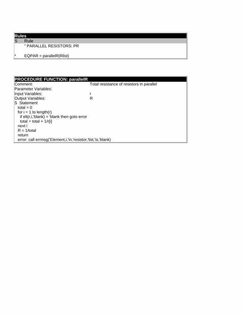
Rules S Rule " PARALLEL RESISTORS: PR * EQPAR = parallelR(Rlist)
PROCEDURE FUNCTION: parallelR Comment: Total resistance of resistors in parallel Parameter Variables: Input Variables: r Output Variables: R S Statement total = 0 for i = 1 to length(r) if elt(r,i,'blank) = 'blank then goto error total = total + 1/r[i] next i R = 1/total return error: call errmsg('Element,i,'in,'resistor,'list,'is,'blank)

ELECTRICAL ENGINEERING SOLVERPACK PART 2 OF 2
Standard Resistor Values
Filename: SRV.TK
Useful for: Section 3, Standard Measurement Techniques for Resistance, page 41 and following; Section 29, Standards, page 53.
Given a resistor's design value and tolerance, this model will calculate the nearest suitable standard-value resistor.
Variables St Input Name Output Unit Comment STANDARD RESISTOR VALUES: SRV 523 cv Ohm Component value 5 t % Tolerance (%) SV 510 Ohm Standard value Rules S Rule " STANDARD RESISTOR VALUES: SRV * t4 = 1.19927e-2*int(1+1.5*t+.004*t^2) * t3 = int(ln(cv)/ln(10)-int(2.2-3*t4)) * cvtemp = cv/10^t3 * temp = int(ln(cvtemp)/t4) * t1temp = int(exp(t4*temp)+.5) * t2temp = int(exp(t4*(temp+1))+.5) * t5temp = 1.88e-5*t1temp^3 - .00335*t1temp^2 + .164*t1temp - 1.284 * t1 = t1temp + int(t5temp*int(3*t4+.8)) * t5 = 1.88e-5*t2temp^3 - .00335*t2temp^2 + .164*t2temp - 1.284 * t2 = t2temp + int(t5*int(3*t4+.8)) * testval = int(cvtemp/sqrt(t1*t2)+1) * sv1 = 10^t3*t1 * sv2 = 10^t3*t2 * SV = (testval = 1)*sv1+(testval = 2)*sv2
Bypass Capacitor Calculation
Filename: BCC.TK

Useful for: Section 2, page 30 and following; Section 2, page 41; Section 16, page 79 and following.
Given a range of frequencies of current being bypassed and the value of the resistance of the resistor being bypassed, this model calculates the value of the capacitor needed to do the job in the emitter leg of a circuit.
Alternatively, if the capacitance and frequency are known, the resistance can be determined. Or if values of both components are fixed, the model calculates the lowest safe frequency for operating the circuit.
Variables St Input Name Output Unit Comment BYPASS CAPACITOR CALCULATION: BCC 60 bf Hz Lowest frequency being bypassed 200 br Ohm Value of resistance being bypassed BC 132.62912 uF Bypass capacitance
Rules S Rule " BYPASS CAPACITOR CALCULATION: BCC * BC = 1e7/(2*pi()*bf*br)
Power-Supply Interruption
Filename: PSIT.TK
Useful for: Section 5, Emergency Generators, page 63; Section 28, Uninterruptible Power Supplies, page 5 and following; Section 29, Standards, page 50 and following:
The most common use of this model will be to calculate how long the main power supply will continue to provide a regulated voltage to a load, after all outside power has been cut.
Designers can also work backward, given a desired voltage up time, to change voltage parameters, amperage, or storage capacitor size in order to match system needs. (A circuit connected to an emergency power supply with a 20-millisecond cut-in time might need a larger storage capacitor to continue stable operation or a higher tolerated voltage drop at the regulator.)
Variables St Input Name Output Unit Comment

POWER SUPPLY INTERRUPT TIME: PSIT 16 voltin V Unregulated voltage 3 drop V Minimum regulator drop 12 load V Load voltage 2 current A Load current 20000 cap uF Storage capacitor UP 10 mS Regulated voltage up time
Rules S Rule " POWER SUPPLY INTERRUPT TIME: PSIT * UP = ((voltin-drop-load)*cap)/current*1000
Schmitt Trigger Design
Filename: STD.TK
Useful for: Section 13, Solid-State Power Devices, page 4 and following; Section 16, Power-Line Carriers, page 104 and following; Section 26, Signal Devices, page 62.
A Schmitt trigger is a circuit that has two stable states - a high-voltage output and a low-voltage output - depending on the input. A typical configuration for this circuit would be a transistor operational amplifier in parallel with a resistor. A steady supply voltage is applied to one side of the assemblage ("supply" in the model) and a variable voltage is applied between base and emitter.
In the example, a nominal upper threshold of 9 volts is "triggered" at 8.967033 volts, given the loads and (standardized) resistances.
FIG. 7

Variables St Input Name Output Unit Comment SCHMITT TRIGGER DESIGN: STD 9 upper V Upper threshold voltage 5 lower V Lower threshold voltage 12 supply V Enter supply voltage .6 emitter V Emitter-base voltage 300 load Ohm Load impedance 5 t % Resistor tolerance R1 680 Ohm Resistor R1 R2 1200 Ohm Resistor R2 R3 6800 Ohm Resistor R3 R4 1100 Ohm Resistor R4 PD 45.8 mW Power dissipated by the load UP 8.967033 V Upper threshold LOW 4.9404255 V Lower threshold
Rules S Rule " SCHMITT TRIGGER DESIGN: STD * R1t = load*(upper-emitter)/(supply-upper+emitter)

* R1 = CalcStandard(R1t,t) * R2t = R1*(supply-lower+emitter)/(lower-emitter) * R2 = CalcStandard(R2t,t) * R3 = 10*R1 * R4t = R3*supply/upper - R3 - R2 * R4 = CalcStandard(R4t,t) * temp = (upper-emitter)/R1 * PD = int(10000*temp^2*load+.5)/10 * UP = R3*supply/(R2+R3+R4) * LOW = emitter + R1*supply/(R1+R2)
RULE FUNCTION: CalcStandard Comment: Calculate standard resistor value Parameter Variables: Argument Variables: Rt,t Result Variables: R S Rule cv = Rt t4 = 1.19927e-2*int(1+1.5*t+.004*t^2) t3 = int(ln(cv)/ln(10)-int(2.2-3*t4)) cvtemp = cv/10^t3 t1temp = int(exp(t4*int(ln(cvtemp)/t4))+.5) t5temp = 1.88e-5*t1temp^3 - .00335*t1temp^2 + .164*t1temp - 1.284 t1 = t1temp + int(t5temp*int(3*t4+.8)) t2temp = int(exp(t4*(int(ln(cvtemp)/t4)+1))+.5) t5 = 1.88e-5*t2temp^3 - .00335*t2temp^2 + .164*t2temp - 1.284 t2 = t2temp + int(t5*int(3*t4+.8)) testval = int(cvtemp/sqrt(t1*t2)+1) sv1 = 10^t3*t1 sv2 = 10^t3*t2 R = (testval = 1)*sv1+(testval = 2)*sv2
Resistor Color Codes
Filename: RCC.TK
Useful for: Any circuits where resistors are used.
This model makes use of TK Solver's list functions to calculate resistor values and tolerances. All the user has to do is type the colors of the bands in either upper- or lowercase letters.
FIG. 8

Variables St Input Name Output Unit Comment RESISTOR COLOR CODES: RCC 'brown band1 Band one color code 'yellow band2 Band two color code 'orange band3 Band three color code 'gold band4 Band four color code RV 14 KOhm Resistor value TOL 5 % Tolerance Colors Available:
BLACK BROWN RED ORANGE YELLOW GREEN BLUE PURPLE GREY WHITE GOLD SILVER NONE
Rules S Rule "RESISTOR COLOR CODES: RCC * if member(band1,'colors) = 0 then call errmsg('Band,'one,'color,'misspelled) * if member(band2,'colors) = 0 then call errmsg('Band,'two,'color,'misspelled) * if member(band3,'colors) = 0 then call errmsg('Band,'three,'color,'misspelled) * if member(band4,'tolcolor) = 0 then call errmsg('Band,'four,'color,'misspelled) * RV = (10*colorval(band1)+colorval(band2))*10^colorval(band3) * TOL = toll(given('band4,band4,'none))
LIST FUNCTION: colorval Comment: Return the color value for band 1-3
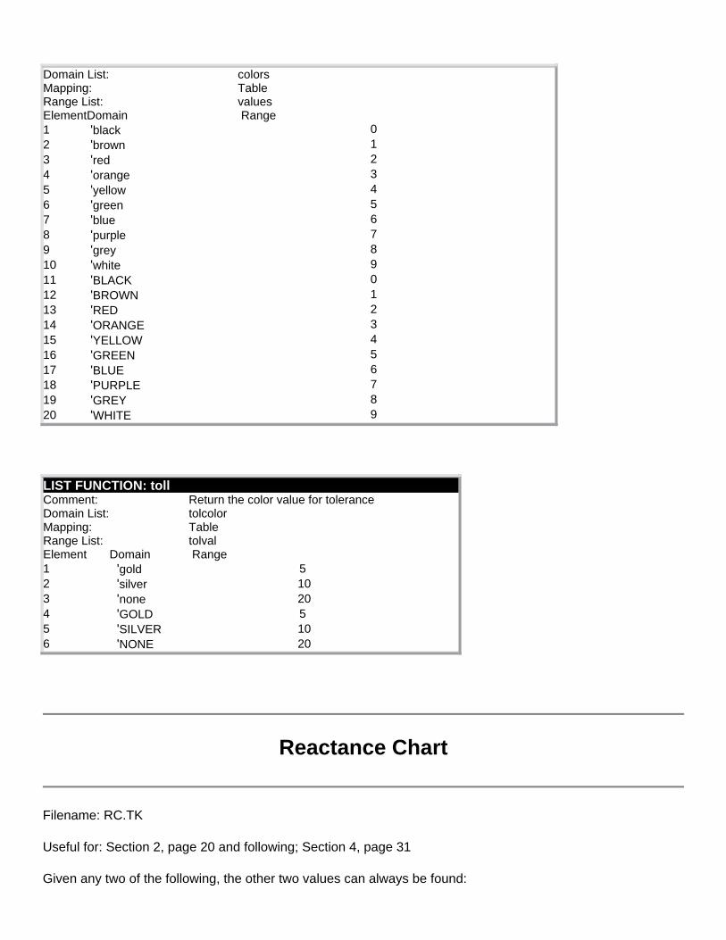
Domain List: colors Mapping: Table Range List: values ElementDomain Range 1 'black 0 2 'brown 1 3 'red 2 4 'orange 3 5 'yellow 4 6 'green 5 7 'blue 6 8 'purple 7 9 'grey 8 10 'white 9 11 'BLACK 0 12 'BROWN 1 13 'RED 2 14 'ORANGE 3 15 'YELLOW 4 16 'GREEN 5 17 'BLUE 6 18 'PURPLE 7 19 'GREY 8 20 'WHITE 9
LIST FUNCTION: toll Comment: Return the color value for tolerance Domain List: tolcolor Mapping: Table Range List: tolval Element Domain Range 1 'gold 5 2 'silver 10 3 'none 20 4 'GOLD 5 5 'SILVER 10 6 'NONE 20
Reactance Chart
Filename: RC.TK
Useful for: Section 2, page 20 and following; Section 4, page 31
Given any two of the following, the other two values can always be found:

Resonant frequency
Inductance
Capacitance
Reactance
Variables St Input Name Output Unit Comment REACTANCE CHART: RC 3.2 f MHz Resonant frequency L 9.8946468 uHenry Inductance 250 C pF Capacitance X 198.94368 Ohm Reactance
Rules S Rule " REACTANCE CHART: RC * f = (1/(2*pi()*sqrt(L*C))) * X = (1/(2*pi()*f*C)) * f = X/(2*pi()*L)
Passive High- and Low-Pass Composite Filter Design
Filename: PHALCFD.TK
Useful for: Section 2, page 52 and following; Section 16, page 71 and following. See also Section 14, PI and T Nominal Representations, pages 22 and 23.
This model allows design of high- and low-pass filters for specific frequencies (Fc in model's notation, in book's) under either the "prototype" or "transfer function" ("m" in the model's notation, G in the book's) point of view. See, in particular, Section 2, page 71 and following, and model AFD.TK.
Backsolving is mathematically possible (and often worthwhile) in this model for "reverse engineering" a filter based on its actual measured performance at a given range of frequencies.

Variables St Input Name Output Unit Comment PASSIVE HIGH AND LOWPASS COMPOSITE FILTER DESIGN: PHALCFD 10000 Fc Hz Cut-off frequency 100 R Ohm Image impedance .5 LPm Desired 'm' for low pass filter LPF00 11547.005 Hz Freq. of infinite attenuation (LP) HPm .99997887 Desired 'm' for high pass filter 65 HPF00 Hz Freq. of infinite attenuation (HP) LOW PASS FILTER: T Prototype: LPCk 3.1831E-7 F Ck LPLkh .00159155 Henry 1/2 Lk Pi Prototype: LPCkh 1.5915E-7 F 1/2 Ck LPLk .0031831 Henry Lk M-derived-T: LPLb .00119366 Henry Lb LPCb 1.5915E-7 F Cb LPLah .00079577 Henry 1/2 La M-derived-Pi: LPCbh 7.9577E-8 F 1/2 Cb LPLa .00159155 Henry La LPCa 1.1937E-7 F Ca HIGH PASS FILTER: T Prototype: HPLk .00079577 Henry Lk HPCkd 1.5915E-7 F 2 Ck Pi Prototype: HPLkd .00159155 Henry 2 Lk HPCk 7.9577E-8 F Ck M-derived-T: HPCb .0075338 F Cb HPLb .00079579 Henry Lb HPCad 1.5916E-7 F 2 Ca M-derived-Pi: HPLbd .00159158 Henry 2 Lb HPCa 7.9579E-8 F Ca HPLa 75.338026 Henry La

Rules S Rule " PASSIVE HIGH AND LOWPASS COMPOSITE FILTER DESIGN: PHALCFD " Low pass filter: * LPm = sqrt(1-(Fc/LPF00)^2) * LPLk = R/(pi()*Fc) * LPLkh = LPLk/2 * LPLa = LPm*LPLk * LPLah = LPLa/2 * LPLb = (1-LPm^2)/(4*LPm)*LPLk * LPCk = 1/(pi()*R*Fc) * LPCkh = LPCk/2 * LPCb = LPm*LPCk * LPCbh = LPCb/2 * LPCa = (1-LPm^2)/(4*LPm)*LPCk " High pass filter: * HPm = sqrt(1-(HPF00/Fc)^2) * HPLk = R/(4*pi()*Fc) * HPLkd = HPLk*2 * HPLb = HPLk/HPm * HPLbd = HPLb*2 * HPLa = (4*HPm)/(1-HPm^2)*HPLk * HPCk = 1/(4*pi()*R*Fc) * HPCkd = HPCk*2 * HPCa = HPCk/HPm * HPCad = HPCa*2 * HPCb = (4*HPm)/(1-HPm^2)*HPCk
Active Filter Design
Filename: AFD.TK
Useful for: Section 2, page 52 and following; Section 13, page 60; Section 16, page 71.
Use this model to calculate resistor and capacitor values for prototype low-pass, high-pass, and bandpass filters.
FIG. 9

FIG. 10

Variables St Input Name Output Unit Comment ACTIVE FILTER DESIGN: AFD 10 F0 Hz Center frequency 10 A Midband gain 1 pf Peaking factor .000001 C F Capacitor value Low pass filter: LPR1 795.77472 F R1 LPC2 .000044 F C2 LPR3 723.43156 F R3 LPR4 7957.7472 F R4 LPC5 .000001 F C5 High pass filter: HPC1 .000001 F C1 HPR2 7578.8068 F R2 HPC3 .000001 F C3 HPC4 .0000001 F C4 HPR5 334225.38 F R5 Band pass filter: BPR1 1591.5494 F R1 BPR2 -1989.437 F R2 BPC3 .000001 F C3 BPC4 .000001 F C4 BPR5 31830.989 F R5
Rules S Rule " ACTIVE FILTER DESIGN: AFD " Low pass filter calculations: * LPR1 = pf/2/A/(2*pi()*F0*C) * LPC2 = C*4*(A+1)/pf^2 * LPR3 = pf/2/(A+1)/(2*pi()*F0*C) * LPR4 = A*LPR1 * LPC5 = C " High pass filter calculations: * HPC1 = C * HPC3 = C * HPC4 = C/A * HPR2 = pf/(2*pi()*F0*C)/(2+1/A) * HPR5 = (A*2+1)/pf/(2*pi()*F0*C) " Band pass filter calculations: * BPR1 = 1/(2*pi()*F0*C*A*pf) * BPR2 = 1/((2/pf^2-A)*2*pi()*F0*C*pf) * BPR5 = 2/pf/(2*pi()*F0*C)

* BPC3 = C * BPC4 = C
Butterworth Filter Design
Filename: BFD.TK
Useful for: Section 2, page 55 and following
The Butterworth approximation is particularly suitable for low-pass filters.
The results are in lists named C and L, which are arranged in a table in the table sheet. In C all even-numbered elements will be zero; in L all odd-numbered elements will be zero.
FIG. 11
Variables St Input Name Output Unit Comment BUTTERWORTH FILTER DESIGN: BFD

9 n Filter order 0 e db Ripple 2000 r Ohm Termination 10000 fc Hz fc Results are shown in Table Sheet
Rules S Rule " BUTTERWORTH FILTER DESIGN: BFD * call BFD()
PROCEDURE FUNCTION: BFD Comment: Butterworth Filter Design Parameter Variables: fc,n,r Input Variables: Output Variables: S Statement - call blank('n) call blank('C) call blank('L) for i = 1 to n step 2 'n[i] = i 'C[i] = (1/(pi()*fc*r))*sin((2*i-1)*pi()/(2*n)) 'L[i] = 0 next i for j = 2 to n step 2 'n[j] = j 'C[j] = 0 'L[j] = (r/(pi()*fc))*sin((2*j-1)*pi()/(2*n)) next j
Table Title: BUTTERWORTH FILTER DESIGN
COMPONENT VALUES Element i Ci Li 1 1 2.7637E-9 0 2 2 0 .031830989 3 3 1.2192E-8 0 4 4 0 .05982269 5 5 1.59155E-8 0 6 6 0 .05982269 7 7 1.2192E-8 0 8 8 0 .031830989 9 9 2.7637E-9 0

Reactive Network Impedance Matching
Filename: RLNIM.TK
Useful for: Section 15, page 36 and following
Given the source and load impedances (each divided into a resistive and a reactive part), this model defines the two possible pure reactive networks that can match them.
Although the equations for the two networks are essentially mirror images (subscripts are reversed), the network values themselves are not mirror images. The example clearly shows this.
Variables St Input Name Output Unit Comment REACTIVE L NETWORK IMPEDANCE MATCHING: RLNIM 50 Xl Ohm Load impedance reactive part 50 Rl Ohm Load impedance resistive part 50 Xs Ohm Source impedance reactive part 25 Rs Ohm Source impedance resistive part First network: X11p -36.60254 Ohm Shunt reactance (+) X21p -6.69873 Ohm Series reactance (+) X11m 136.60254 Ohm Shunt reactance (-) X21m -93.30127 Ohm Series reactance (-) Second network: X12p -161.2372 Ohm Shunt reactance (+) X22p -111.2372 Ohm Series reactance (+) X12m -38.76276 Ohm Shunt reactance (-) X22m 11.237244 Ohm Series reactance (-)
Rules S Rule " REACTIVE L NETWORK IMPEDANCE MATCHING: RLNIM

* alm1 = Rs*Xl/(Rs-Rl) * alm2 = Rl*Xs/(Rl-Rs) * alm3 = Rs*(Xl^2+Rl^2)/(Rs-Rl) * alm4 = Rl*(Xs^2+Rs^2)/(Rl-Rs) " Calculate X1 & X2 for for first network (+): * X11p = -(alm1+sqrt(alm1^2-alm3)) * X21p = (Rs*(X11p+Xl)-Rl*(X11p+Xs))/Rl " Calculate X1 & X2 for for first network (-): * X11m = -(alm1-sqrt(alm1^2-alm3)) * X21m = (Rs*(X11m+Xl)-Rl*(X11m+Xs))/Rl " Calculate X1 & X2 for for second network (+): * X12p = -(alm2+sqrt(alm2^2-alm4)) * X22p = (Rl*(X12p+Xs)-Rs*(X12p+Xl))/Rs " Calculate X1 & X2 for for second network (-): * X12m = -(alm2-sqrt(alm2^2-alm4)) * X22m = (Rl*(X12m+Xs)-Rs*(X12m+Xl))/Rs
Coil Calculations
Filename: CC.TK
Useful for: Section 2, page 21 and following; Section 7, page 5 and following
Equations for three different types of coils are included here: single-layer coils, multilayer coils, and single-spiral coils. The model calculates diameter, length, self-inductance, and number of turns. In general, any one variable can be found if the others are known for a given coil type.
Because this model combines three separate sets of equations, the notation differs from that of the book. L, the self inductance, becomes s1L (for single-layer coils), m1L (for multilayer coils), and ssL (for single-spirals). Other variables are transformed the same way, except that s1r, m1r, and ssr refer to coil diameter rather than coil radius. (The book uses R for radius.)
Variables St Input Name Output Unit Comment COIL CALCULATIONS: CC .5 slr in r diameter (single layer coil) 2 sll in Length (single layer coil) 100 slL uHenry Self-inductance (single layer coil) slN 98.994949 Number of turns (single layer coil) .5 mlr in r diameter (multi-layer coil) 2 mll in Length (multi-layer coil) .8 mlb in b diameter (multi-layer coil) mlL 17.241379 uHenry Self-inductance (multi-layer coil)

50 mlN Number of turns (multi-layer coil) .5 ssr in r diameter (single spiral coil) .8 ssb in b diameter (single spiral coil) 100 ssL uHenry Self-inductance (single spiral coil) ssN 71.554175 Number of turns (single spiral coil)
Rules S Rule " COIL CALCULATIONS: CC " Calculations for single layer coil: * slL = (slr^2*slN^2)/(9*slr+10*sll) * slN = sqrt(slL*(9*slr+10*sll))/slr " Calculations for multi-layer coil: * mlL = (.8*mlr^2*mlN^2)/(6*mlr+9*mll+10*mlb) " Calculations for single layer spiral coil: * ssL = (ssr^2*ssN^2)/(8*ssr+11*ssb)
Transmission-Line Impedance
Filename: TLI.TK
Useful for: Section 2, page 23; and Section 14, Transmission Systems
This model will calculate the characteristic impedance for five different types of transmission-line configurations in high-frequency operations. These are:
Open two-wire lines
Single-wire line near ground
Balanced wires near ground
Wires in parallel, near ground
Coaxial lines
Necessary information includes wire spacing, diameter, permittivity, and (for near-ground systems) height from ground. The generalized equations are found in the book, starting on page 12 in Section 14.
In general, the near-ground equations should be followed if wire height is within two wavelengths. The equations hold for frequencies greater than 3 MHz.

Variables St Input Name Output Unit Comment TRANSMISSION LINE IMPEDANCE: TLI .68 D in Wire spacing .195 d in Wire diameter 1 e Relative permitivity 6 h in Wire height High freq. characteristc impedance: OTWL 233.06885 Open two-wire line SWNG 288.44437 Single wire near ground BWNG 232.61504 Balanced wires near ground WPNG 230.29061 Wires in parallel near ground COAX 74.945594 Coaxial line
Rules S Rule " TRANSMISSION LINE IMPEDANCE: TLI " Open two-wire line: * OTWL = 120/sqrt(e)*ln(2*D/d) " Single wire near ground: * SWNG = 138/sqrt(e)*log(4*h/d) " Balanced wires near ground: * BWNG = 276/sqrt(e)*log(2*D/d/sqrt(1+(D/(2*h))^2)) " Wires in parallel near ground: * WPNG = 69/sqrt(e)*log(4*h/d*sqrt(1+(2*h/D)^2)) " Coaxial line: * COAX = 60/sqrt(e)*ln(D/d)
Transmission-Line Exact Calculation
Filename: TLEC.TK
Useful for: Section 14, Transmission Systems
Where r (line resistance) and g (substrate conductance) are known with certainty, this model will calculate the impedance magnitude and angle of a loss-line transmission.
If r and g are not known, use the following model, TLAC.TK, instead.
The equations used are:

R0 = sqrt(L/C)
r = R/L = R/R0
g = G/C = R0G
= 2 ƒ
Zln = [Z0] [(1 + L e-2 ) / (1 - L e-2 )
Re{Z0} = [R0 / sqrt(2(g2 + 2))] [rg + 2 + sqrt((r2 + 2)(g2 + 2))]½
Im{Z0} = [±R0/ sqrt(2(g2+ 2))] [-(rg + 2) + sqrt((r2 + 2)(g2 + 2))]½
in which the + sign is chosen when g >= r and the - sign is chosen when g < r.
= [1 / ( )] [rg - 2+ sqrt((r2+ 2)(g2 + 2))]½
= [1 / ( )] [ 2- rg + sqrt((r2+ 2)(g2 + 2))]½
Variables St Input Name Output Unit Comment TRANSMISSION LINE EXACT CALCULATION: TLEC 2E9 f Hz Frequency .85 vr Relative phase velocity 55 r0 Ohm Characteristic impedance line loss 3.5 l cm Line length .00004187 g Siemens Conductance of substrate per unit 1.2664 r Ohm Resistance of line per unit 75 zlmag Magnitude of terminating impedance -30 zlang Angle of terminating impedance Zinmag 48.007836 Z(in) magnitude Zinang 28.479855 deg Z(in) angle
Rules S Rule " TRANSMISSION LINE EXACT CALCULATION: TLEC * x1 = r*3*vr/r0 * y1 = f/1e10*2*pi() * (mag1,ang1) = rtopd(x1,y1) * x2 = 3*vr*g*r0 * y2 = f/1e10*2*pi() * (mag2,ang2) = rtopd(x2,y2) * mag3 = l*2/(3*vr)*sqrt(mag1)*sqrt(mag2) * ang3 = ang2/2 + ang1/2

* (x3,y3) = ptord(mag3,ang3) * mag31 = zlmag/(r0*sqrt(mag1)/sqrt(mag2)) * ang31 = zlang-(ang1/2-ang2/2) * (x31,y31) = ptord(mag31,ang31) * x4 = x31 + 1 * y4 = y31 * (mag4,ang4) = rtopd(x4,y4) * mag41 = -2/mag4 * ang41 = -ang4 * (x41,y41) = ptord(mag41,ang41) * x5 = x41 + 1 * y5 = y41 * (mag5,ang5) = rtopd(x5,y5) * mag6 = 1/(mag5*exp(-x3)) * ang6 = y3*180/pi( ) - ang5 * (x6,y6) = ptord(mag6,ang6) * x7 = x6 -1 * y7 = y6 * (mag7,ang7) = rtopd(x7,y7) * mag8 = 2/mag7 * ang8 = -ang7 * (x8,y8) = ptord(mag8,ang8) * x9 = x8 + 1 * y9 = y8 * (mag9,ang9) = rtopd(x9,y9) * Zinmag = mag9*r0*sqrt(mag1)/sqrt(mag2) * Zinang = ang9 + ang1/2 - ang2/2