Embed Size (px)
Citation preview

CS1026 1
A low resistivity indicates a material that A low resistivity indicates a material that readily allows the movement of electric charge. readily allows the movement of electric charge. Resistivity is commonly represented by the Resistivity is commonly represented by the Greek letter ρ.Greek letter ρ.
The SI unit of electrical resistivity is the The SI unit of electrical resistivity is the ohm metre (Ω m)⋅ ⋅ohm metre (Ω m)⋅ ⋅Electrical conductivity is the reciprocal of Electrical conductivity is the reciprocal of electrical resistivity.electrical resistivity.If a 1 m × 1 m × 1 m solid cube of material has If a 1 m × 1 m × 1 m solid cube of material has sheet contacts on two opposite faces, and the sheet contacts on two opposite faces, and the resistance between these contacts is 1 Ω, then resistance between these contacts is 1 Ω, then the resistivity of the material is 1 Ω m.⋅the resistivity of the material is 1 Ω m.⋅
Electrical resistivity quantifies how strongly Electrical resistivity quantifies how strongly a given material opposes the flow of electric a given material opposes the flow of electric current. current.

CS1026 2
In a hydraulic analogy, passing current through In a hydraulic analogy, passing current through a high-resistivity material is like pushing watera high-resistivity material is like pushing waterthrough a pipe full of sand—while passing through a pipe full of sand—while passing current through a low-resistivity material is like current through a low-resistivity material is like pushing water through an empty pipe. pushing water through an empty pipe.
If the pipes are the same size and shape, the pipe full of sand has higher If the pipes are the same size and shape, the pipe full of sand has higher resistance to flow. Resistance, however, is not solely determined by theresistance to flow. Resistance, however, is not solely determined by thepresence or absence of sand. It also depends on the length and width ofpresence or absence of sand. It also depends on the length and width ofthe pipe: short or wide pipes have lower resistance than narrow or longthe pipe: short or wide pipes have lower resistance than narrow or longpipes. All copper wires, irrespective of their shape and size, have pipes. All copper wires, irrespective of their shape and size, have approximately the same resistivity, but a long, thin copper wire has a approximately the same resistivity, but a long, thin copper wire has a much larger resistance than a thick, short copper wire. much larger resistance than a thick, short copper wire.

CS1026 3
Drude model was proposed in 1900 by Paul Drude model was proposed in 1900 by Paul Drude to explain the transport properties of Drude to explain the transport properties of electrons in materials.electrons in materials.
The Drude model treats electrons (or other charge The Drude model treats electrons (or other charge carriers) like pinballs bouncing among the ions that carriers) like pinballs bouncing among the ions that make up the structure of the material. make up the structure of the material.
Electrons will be accelerated in the opposite direction to Electrons will be accelerated in the opposite direction to the electric field by the average electric field at their the electric field by the average electric field at their location. location.
With each collision, though, the electron is deflected With each collision, though, the electron is deflected in a random direction with a velocity that is much larger in a random direction with a velocity that is much larger than the velocity gained by the electric field. than the velocity gained by the electric field.
The net result is that electrons take a zigzag path due to the The net result is that electrons take a zigzag path due to the collisions, but generally drift in a direction opposing collisions, but generally drift in a direction opposing the electric field.the electric field.

CS1026 4
This simple classical Drude model provides a very good explanation of DC This simple classical Drude model provides a very good explanation of DC and AC resistivity in metalsand AC resistivity in metals
Electrical resistivity (also known as resistivity, specific electrical resistance, or Electrical resistivity (also known as resistivity, specific electrical resistance, or volume resistivity) is an intrinsic property that quantifies how strongly a given volume resistivity) is an intrinsic property that quantifies how strongly a given material opposes the flow of electric currentmaterial opposes the flow of electric current
The resistance of a given object depends primarily on two factors: What material itThe resistance of a given object depends primarily on two factors: What material itis made of, and its shape. is made of, and its shape.
For a given material, the resistance is inversely proportional to the cross-sectional For a given material, the resistance is inversely proportional to the cross-sectional area; for example, a thick copper wire has lower resistance than an otherwisearea; for example, a thick copper wire has lower resistance than an otherwiseidentical thin copper wire. identical thin copper wire.
Also, for a given material, the resistance is proportional to the length; for example, Also, for a given material, the resistance is proportional to the length; for example, a long copper wire has higher resistance than an otherwise-identical short copper wire.a long copper wire has higher resistance than an otherwise-identical short copper wire.
Electrical resistance shares some conceptual parallels with the mechanical notion ofElectrical resistance shares some conceptual parallels with the mechanical notion offrictionfriction

CS1026 5
Ohm's Law - the most fundamental formula in electrical engineeringOhm's Law - the most fundamental formula in electrical engineering
Georg Simon Ohm (16 March 1789 – 6 July 1854) was Georg Simon Ohm (16 March 1789 – 6 July 1854) was a German physicist and mathematician.a German physicist and mathematician.
Ohm's LawOhm's Law
The law states that the direct current flowing in a The law states that the direct current flowing in a conductor is directly proportional to the potential difference conductor is directly proportional to the potential difference between its ends. It is usually formulated as V = IR, where between its ends. It is usually formulated as V = IR, where V is the potential difference, or voltage, I is the current, V is the potential difference, or voltage, I is the current, and R is the resistance of the conductor.and R is the resistance of the conductor.

CS1026 6
As the electrons bump their way through the material As the electrons bump their way through the material we must keep applying external energy towe must keep applying external energy tokeep them moving. Each time the electrons collide keep them moving. Each time the electrons collide with the resistor atoms, the electrical kineticwith the resistor atoms, the electrical kineticenergy is given to the resistor atoms heating them up.energy is given to the resistor atoms heating them up. Thus, one parameter that is specified with theThus, one parameter that is specified with theresistance value is the ability of the resistance to resistance value is the ability of the resistance to pass its heat energy safely to the surrounding air.pass its heat energy safely to the surrounding air.

CS1026 7
ResistorsResistors
The electrical resistance of an The electrical resistance of an electrical conductor is the opposition electrical conductor is the opposition to the passage of an electric current to the passage of an electric current through that conductor. through that conductor.
The SI unit of electrical resistance is The SI unit of electrical resistance is the ohm (Ω).the ohm (Ω).
For a wide variety of materials and For a wide variety of materials and conditions, V and I are directly conditions, V and I are directly proportional to each other. proportional to each other.
This proportionality is called Ohm's law, This proportionality is called Ohm's law, and materials that satisfy it are called and materials that satisfy it are called "Ohmic" materials."Ohmic" materials.
A resistor is a passive two-terminal electrical component that implements electrical resistance as a A resistor is a passive two-terminal electrical component that implements electrical resistance as a circuit element.circuit element.

A semiconductor has electrical conductivity intermediate to that A semiconductor has electrical conductivity intermediate to that of a conductor and an insulator.of a conductor and an insulator.
Semiconductor materials are useful because their behaviour can Semiconductor materials are useful because their behaviour can be manipulated by the addition of impurities, known as doping. be manipulated by the addition of impurities, known as doping.
The comprehensive theory of semiconductors relies on the The comprehensive theory of semiconductors relies on the principles of quantum physics to explain the motions of electrons principles of quantum physics to explain the motions of electrons through a lattice of atoms.through a lattice of atoms.
SEMICONDUCTORSSEMICONDUCTORS

Variable conductivityVariable conductivity
A pure semiconductor is a poor electrical conductor as a consequence of A pure semiconductor is a poor electrical conductor as a consequence of having just the right number of electrons to completely fill its valence having just the right number of electrons to completely fill its valence bonds. bonds.
Through various techniques (e.g., doping or gating), the semiconductor Through various techniques (e.g., doping or gating), the semiconductor can be modified to have excess of electrons (becoming an n-type can be modified to have excess of electrons (becoming an n-type semiconductor) or a deficiency of electrons (becoming a p-type semiconductor) or a deficiency of electrons (becoming a p-type semiconductor). semiconductor).
In both cases, the semiconductor becomes much more conductive (the In both cases, the semiconductor becomes much more conductive (the conductivity can be increased by one million fold or more). conductivity can be increased by one million fold or more). Semiconductor devices exploit this effect to shape electrical current.Semiconductor devices exploit this effect to shape electrical current.

A semiconductor has electrical conductivity intermediate to that A semiconductor has electrical conductivity intermediate to that of a conductor and an insulatorof a conductor and an insulator
Electrical resistivity is a property of a material; it quantifies how Electrical resistivity is a property of a material; it quantifies how strongly the material opposes the flow of electric currentstrongly the material opposes the flow of electric current
In copper, every single copper atom donates one movable In copper, every single copper atom donates one movable electron to the "sea of charge." electron to the "sea of charge."
Copper's "electric fluid" is very dense; just as dense as the Copper's "electric fluid" is very dense; just as dense as the copper metalcopper metal
In doped silicon, only one in every billion atoms donates a In doped silicon, only one in every billion atoms donates a movable charge. Silicon is like a big empty space with an movable charge. Silicon is like a big empty space with an occasional wandering chargeoccasional wandering charge
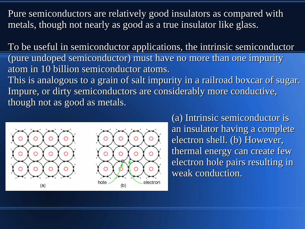
Pure semiconductors are relatively good insulators as compared with Pure semiconductors are relatively good insulators as compared with metals, though not nearly as good as a true insulator like glass. metals, though not nearly as good as a true insulator like glass.
To be useful in semiconductor applications, the intrinsic semiconductor To be useful in semiconductor applications, the intrinsic semiconductor (pure undoped semiconductor) must have no more than one impurity (pure undoped semiconductor) must have no more than one impurity atom in 10 billion semiconductor atoms. atom in 10 billion semiconductor atoms. This is analogous to a grain of salt impurity in a railroad boxcar of sugar. This is analogous to a grain of salt impurity in a railroad boxcar of sugar. Impure, or dirty semiconductors are considerably more conductive, Impure, or dirty semiconductors are considerably more conductive, though not as good as metals.though not as good as metals.
(a) Intrinsic semiconductor is (a) Intrinsic semiconductor is an insulator having a complete an insulator having a complete electron shell. (b) However, electron shell. (b) However, thermal energy can create few thermal energy can create few electron hole pairs resulting in electron hole pairs resulting in weak conduction.weak conduction.

DopingDoping
Pure semiconductors, by themselves, are not particularly useful. Though, Pure semiconductors, by themselves, are not particularly useful. Though, semiconductors must be refined to a high level of purity as a starting semiconductors must be refined to a high level of purity as a starting point prior the addition of specific impurities.point prior the addition of specific impurities.
Semiconductor material pure to 1 part in 10 billion, may have specific Semiconductor material pure to 1 part in 10 billion, may have specific impurities added at approximately 1 part per 10 million to increase the impurities added at approximately 1 part per 10 million to increase the number of carriers. The addition of a desired impurity to a semiconductor number of carriers. The addition of a desired impurity to a semiconductor is known as doping. Doping increases the conductivity of a semiconductor is known as doping. Doping increases the conductivity of a semiconductor so that it is more comparable to a metal than an insulator.so that it is more comparable to a metal than an insulator.

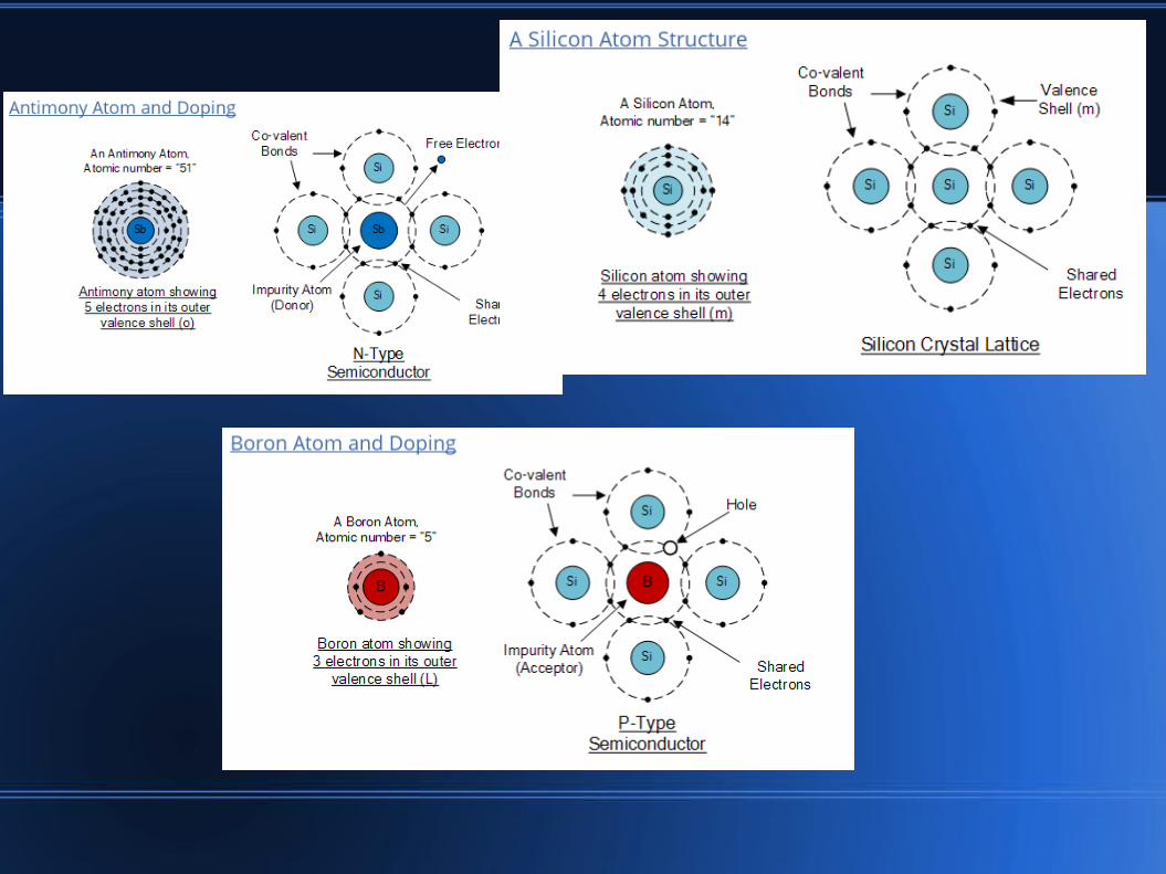
It is possible to increase the It is possible to increase the number of negative charge number of negative charge carriers within the carriers within the semiconductor crystal semiconductor crystal lattice by doping with an lattice by doping with an electron donor like electron donor like Phosphorus. Electron donors, Phosphorus. Electron donors, also known as N-type dopants also known as N-type dopants include elements from group include elements from group VA of the periodic table: VA of the periodic table: nitrogen, phosphorus, nitrogen, phosphorus, arsenic, and antimony. It is arsenic, and antimony. It is also possible to introduce an also possible to introduce an impurity lacking an electron impurity lacking an electron as compared with silicon, as compared with silicon, having three electrons in the valence shell as compared with four for having three electrons in the valence shell as compared with four for silicon. This leaves an empty spot known as a hole, a positive charge silicon. This leaves an empty spot known as a hole, a positive charge carrier. The P-type elements from group IIIA of the periodic table carrier. The P-type elements from group IIIA of the periodic table include: boron, aluminum, gallium, and indium.include: boron, aluminum, gallium, and indium.

If a piece of pure silicon is surrounded by a gas containing boron or phosphorus andIf a piece of pure silicon is surrounded by a gas containing boron or phosphorus andheated in a high-temperature oven, the boron or phosphorus atoms will permeateheated in a high-temperature oven, the boron or phosphorus atoms will permeatethe crystal lattice and displace some silicon atoms without disturbing other atomsthe crystal lattice and displace some silicon atoms without disturbing other atomsin the vicinityin the vicinity
Boron atoms have only three electrons in their outermostBoron atoms have only three electrons in their outermostelectron shells, phosphorous atoms have five electrons in electron shells, phosphorous atoms have five electrons in their outermost electron shellstheir outermost electron shells

Lithography originally used an image drawn with oil, fat, or wax onto the surface of a smooth, level lithographic limestone plate.
The stone was treated with a mixture of acid and gum arabic,etching the portions of the stone which were not protected by the grease-based image.
When the stone was subsequently moistened, these etched areas retained water; an oil-based ink could then be applied and would be repelled by the water, sticking only to the original drawing.
Lithography

The word lithography comes from the Greek lithos, meaning stones, The word lithography comes from the Greek lithos, meaning stones, and graphia, meaning to write. It means quite literally writing on stones. and graphia, meaning to write. It means quite literally writing on stones.
In the case of semiconductor photolithography, In the case of semiconductor photolithography, our stones are silicon wafers and our patterns are our stones are silicon wafers and our patterns are written with a light-sensitive polymer called written with a light-sensitive polymer called photoresist. photoresist.
To build the complex structures that make up a To build the complex structures that make up a transistor and the many wires that connect the transistor and the many wires that connect the millions of transistors of a circuit, lithography millions of transistors of a circuit, lithography and pattern transfer steps are repeated at least 10 times, but more and pattern transfer steps are repeated at least 10 times, but more typically are done 20 to 30 times to make one circuit. typically are done 20 to 30 times to make one circuit.
Each pattern being printed on the wafer is aligned to the previously Each pattern being printed on the wafer is aligned to the previously formed patterns and slowly the conductors, insulators, and selectively formed patterns and slowly the conductors, insulators, and selectively doped regions are built up to form the final device.doped regions are built up to form the final device.

Electron flow in an N-type semiconductor is similar to electrons moving Electron flow in an N-type semiconductor is similar to electrons moving in a metallic wire. The P-type dopant, an electron acceptor, yields in a metallic wire. The P-type dopant, an electron acceptor, yields localized regions of positive charge known as holes. Electron flow is out localized regions of positive charge known as holes. Electron flow is out of the negative battery terminal, through the P-type bar, returning to the of the negative battery terminal, through the P-type bar, returning to the positive battery terminal. An electron leaving the positive (left) end of the positive battery terminal. An electron leaving the positive (left) end of the semiconductor bar for the positive battery terminal leaves a hole in thesemiconductor bar for the positive battery terminal leaves a hole in thesemiconductor, that may move to the right. Holes traverse the crystal semiconductor, that may move to the right. Holes traverse the crystal lattice from left to right. At the negative end of the bar an electron from the lattice from left to right. At the negative end of the bar an electron from the battery combines with a hole, neutralizing it. This makes room for another battery combines with a hole, neutralizing it. This makes room for another hole to move in at the positive end of the bar toward the right. Keep inhole to move in at the positive end of the bar toward the right. Keep inmind that as holes move left to right, that it is actually electrons moving in mind that as holes move left to right, that it is actually electrons moving in the opposite direction that is responsible for the apparant hole movement.the opposite direction that is responsible for the apparant hole movement.

In IC resistors, the In IC resistors, the resistance value can be resistance value can be controlled by varying the controlled by varying the concentration of doping concentration of doping impurity and depth of diffusion. The range of resistor values that impurity and depth of diffusion. The range of resistor values that may be produced by the diffusion process varies from ohms to may be produced by the diffusion process varies from ohms to hundreds of kilohms. The typical tolerance, however, may be no hundreds of kilohms. The typical tolerance, however, may be no better than ± 5%, and may even be as high as ± 20%better than ± 5%, and may even be as high as ± 20%
Integrated Circuit ResistorIntegrated Circuit Resistor

DepletionDepletion
When doped semiconductors are joined to metals, to different When doped semiconductors are joined to metals, to different semiconductors, and to the same semiconductor with different doping, semiconductors, and to the same semiconductor with different doping, the resulting junction often strips the electron excess or deficiency out the resulting junction often strips the electron excess or deficiency out from the semiconductor near the junction. from the semiconductor near the junction.
This depletion region is rectifying (only allowing current to flow in one This depletion region is rectifying (only allowing current to flow in one direction), and used to further shape electrical currents in semiconductor direction), and used to further shape electrical currents in semiconductor devices.devices.

In electronics, a diode is a two-terminal electronic component In electronics, a diode is a two-terminal electronic component with asymmetric transfer characteristic, with low (ideally zero) with asymmetric transfer characteristic, with low (ideally zero) resistance to current flow in one direction, and high (ideally resistance to current flow in one direction, and high (ideally infinite) resistance in the other. infinite) resistance in the other.
A semiconductor diode, the most common type today, is a crystalline A semiconductor diode, the most common type today, is a crystalline piece of semiconductor material with a p-n junction connected to two piece of semiconductor material with a p-n junction connected to two electrical terminalselectrical terminals
Semiconductor DiodeSemiconductor Diode
In a diode, the cathode is the In a diode, the cathode is the negative terminal at the pointed negative terminal at the pointed end of the arrow symbol, where end of the arrow symbol, where current flows out of the devicecurrent flows out of the device

Depletion RegionDepletion Region
The P-Type semiconductor has excess holes. The N-Type semiconductor has excess electrons. Due to The P-Type semiconductor has excess holes. The N-Type semiconductor has excess electrons. Due to this difference, some of the electrons get attracted to the corresponding nearest holes and are eliminated this difference, some of the electrons get attracted to the corresponding nearest holes and are eliminated by recombination. This process takes place until an equilibrium is reached in the by recombination. This process takes place until an equilibrium is reached in the surrounding region of the contact surface. surrounding region of the contact surface.
The net result is the diffused electrons The net result is the diffused electrons and holes are gone, leaving behind the and holes are gone, leaving behind the charged ions adjacent to the interface in charged ions adjacent to the interface in a region with no mobile carriers (called a region with no mobile carriers (called the depletion region)the depletion region)If a block of P-type semiconductor is If a block of P-type semiconductor is placed in contact with a block of N-type placed in contact with a block of N-type semiconductor the result is of no value. semiconductor the result is of no value. A single semiconductor crystal A single semiconductor crystal manufactured with P-type material at manufactured with P-type material at one end and N-type material at the other one end and N-type material at the other has some unique properties. has some unique properties.

In semiconductor physics, the depletion region is an insulating region In semiconductor physics, the depletion region is an insulating region within a conductive, doped semiconductor material where the mobile within a conductive, doped semiconductor material where the mobile charge carriers have been diffused away, or have been forced away by charge carriers have been diffused away, or have been forced away by an electric field. The only elements left in the depletion region are an electric field. The only elements left in the depletion region are ionized donor or acceptor impurities.ionized donor or acceptor impurities.
Depletion RegionDepletion Region

Following transfer, the diffused electrons come into contact with Following transfer, the diffused electrons come into contact with holes on the P-side and are eliminated by recombination.holes on the P-side and are eliminated by recombination. Likewise for the diffused holes on the N-side. Likewise for the diffused holes on the N-side.
The net result is the diffused electrons and holes are gone, leaving The net result is the diffused electrons and holes are gone, leaving behind the charged ions adjacent to the interface in a region with behind the charged ions adjacent to the interface in a region with no mobile carriers (called the depletion region). no mobile carriers (called the depletion region).
The Depletion layer appears when electrons fall into holes,The Depletion layer appears when electrons fall into holes,so the silicon has turned into an insulatorso the silicon has turned into an insulator
The uncompensated ions are positive on the N side and negative on the The uncompensated ions are positive on the N side and negative on the P side. P side.
This creates an electric field that provides a force opposing the This creates an electric field that provides a force opposing the continued exchange of charge carriers. continued exchange of charge carriers.
When the electric field is sufficient to arrest further transfer of holes When the electric field is sufficient to arrest further transfer of holes and electrons, the depletion region has reached its equilibriumand electrons, the depletion region has reached its equilibriumdimensions dimensions

A galvanometer is a type of A galvanometer is a type of sensitive ammeter: an instrument sensitive ammeter: an instrument for detecting electric current. It is for detecting electric current. It is an analog electromechanical an analog electromechanical actuator that produces a rotary actuator that produces a rotary deflection of some type of pointer deflection of some type of pointer in response to electric current in response to electric current through its coil in a magnetic field.through its coil in a magnetic field.

If you connect the anode and cathode of If you connect the anode and cathode of the diode you might be able to observe a the diode you might be able to observe a small voltage or current that is small voltage or current that is insignificant.insignificant. This is because the electromagnetic This is because the electromagnetic spectrum that is present in spectrum that is present in our environment by default knocks our environment by default knocks off electrons in the semiconductor off electrons in the semiconductor lattice that constitutes current.lattice that constitutes current.
In the N-type region electrons are the majority carriers and in the In the N-type region electrons are the majority carriers and in the P-type electron "holes" are the majority carriers.P-type electron "holes" are the majority carriers.
If If forward-biased (applying a positive voltage to the P region and a (applying a positive voltage to the P region and a negative voltage to the N region), the depletion region of the diode negative voltage to the N region), the depletion region of the diode decreases. The electrons on the N side are repelled and they move decreases. The electrons on the N side are repelled and they move towards the P side thus reducing the size of the depletion layer. towards the P side thus reducing the size of the depletion layer.
If If reverse-biasedreverse-biased, the depletion region increases because the electrons , the depletion region increases because the electrons are attracted towards the positive voltage and the holes are attracted are attracted towards the positive voltage and the holes are attracted towards the negative voltage, and hence the current gets reduced and the towards the negative voltage, and hence the current gets reduced and the current flowing will be very small, on the order of micro ampscurrent flowing will be very small, on the order of micro amps

At one particular voltage level VAt one particular voltage level Vff called the threshold / firing / called the threshold / firing / cut-off voltage the depletion layer disappears (overwhelmed cut-off voltage the depletion layer disappears (overwhelmed by the charge) and hence from this point on the diode starts by the charge) and hence from this point on the diode starts to conduct very easily. to conduct very easily.
From this point on the diode current increases exponentially to the From this point on the diode current increases exponentially to the voltage applied.voltage applied.

I–V Characteristics of a p–n junction diodeI–V Characteristics of a p–n junction diode
The negative current axis is The negative current axis is on a different scale (showing on a different scale (showing millionths of an amp rather millionths of an amp rather than thousandths) this is so wethan thousandths) this is so wecan indicate the very small can indicate the very small leakage current which flowsleakage current which flowsdue to electron hole pair due to electron hole pair generation (ie due to the generation (ie due to the natural conduction properties natural conduction properties of the pure silicon). The of the pure silicon). The leakage current flows in both directions but is too small to indicate on leakage current flows in both directions but is too small to indicate on the current scale used on the forward part of the characteristic. the current scale used on the forward part of the characteristic.
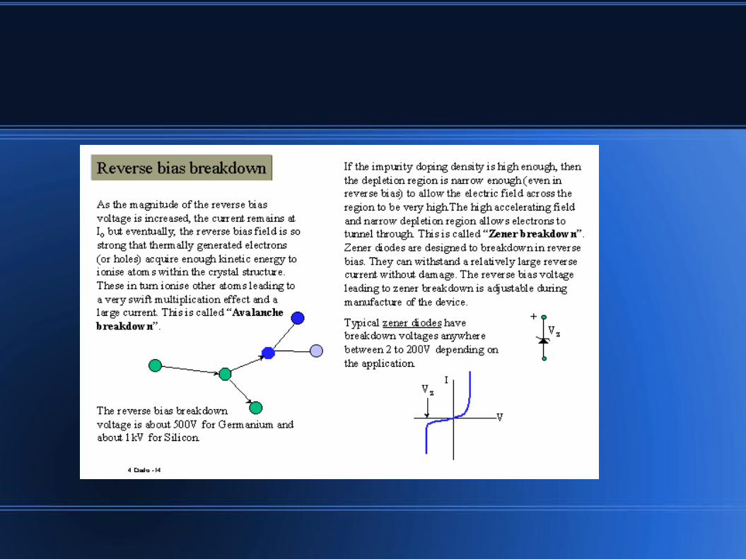
If a large enough reversed bias voltage is applied the diode will If a large enough reversed bias voltage is applied the diode will eventually conduct due to zener then avalanche breakdown (ie due to the eventually conduct due to zener then avalanche breakdown (ie due to the natural conduction properties of the pure silicon). natural conduction properties of the pure silicon).

For silicon diodes, the typical forward voltage is 0.7 volts, nominal. For silicon diodes, the typical forward voltage is 0.7 volts, nominal.
For germanium diodes, the forward voltage is only 0.3 volts. For germanium diodes, the forward voltage is only 0.3 volts.
The chemical constituency of the P-N junction comprising the diode The chemical constituency of the P-N junction comprising the diode accounts for its nominal forward voltage figure, which is why silicon accounts for its nominal forward voltage figure, which is why silicon and germanium diodes have such different forward voltages. and germanium diodes have such different forward voltages.
Forward voltage drop remains approximately constant for a wide range Forward voltage drop remains approximately constant for a wide range of diode currents, meaning that diode voltage drop is not like that of a of diode currents, meaning that diode voltage drop is not like that of a resistor or even a normal (closed) switch. resistor or even a normal (closed) switch.
For most simplified circuit analysis, the voltage drop across a conducting For most simplified circuit analysis, the voltage drop across a conducting diode may be considered constant at the nominal figure and not related to diode may be considered constant at the nominal figure and not related to the amount of current. the amount of current.

Diode logic (DL), or diode-resistor logic (DRL), is the construction of Diode logic (DL), or diode-resistor logic (DRL), is the construction of Boolean logic gates from diodes. Boolean logic gates from diodes. Diode logic was used extensively in the construction of early computersDiode logic was used extensively in the construction of early computers
If either input (A or B) is at If either input (A or B) is at ground potential (logic 0), then dueground potential (logic 0), then dueto the higher potential on the anodeto the higher potential on the anodeside due to the positive voltage from side due to the positive voltage from resistor R, current will flow throughresistor R, current will flow throughthe diode(s) and the voltage on the the diode(s) and the voltage on the output will be equal to the forward output will be equal to the forward voltage of the diode, 0.5v.voltage of the diode, 0.5v.
If both inputs to the AND gate are If both inputs to the AND gate are high (logic 1), then no current will high (logic 1), then no current will pass through either diode, and the pass through either diode, and the positive voltage through R will positive voltage through R will appear on the outputappear on the output

Current flows through a diode in the direction of the arrow.Current flows through a diode in the direction of the arrow.
In the case of the OR gate, if there In the case of the OR gate, if there is no potential (i.e. logic 0, oris no potential (i.e. logic 0, orground) on both inputs, no current ground) on both inputs, no current will pass through either diode, and will pass through either diode, and the pull-down resistor R will the pull-down resistor R will keep the output at ground (logic 0).keep the output at ground (logic 0).
If either of the inputs has a If either of the inputs has a positive (logic 1) positive (logic 1) voltage on its input (a or b),voltage on its input (a or b),then current will pass through the then current will pass through the diode(s) and appear on the output diode(s) and appear on the output less the forward voltage of the diode (aka diode drop).less the forward voltage of the diode (aka diode drop).

While diode logic has the advantage of simplicity, the lack of an While diode logic has the advantage of simplicity, the lack of an amplifying stage in each gate limits its application.amplifying stage in each gate limits its application.
Also note that it is not possible to construct an inverter with only diodes Also note that it is not possible to construct an inverter with only diodes and resistors. AND and OR functions by themselves are not a completeand resistors. AND and OR functions by themselves are not a completelogic without NOT. logic without NOT.
Thus, there are some logic functions that cannot be implemented in Thus, there are some logic functions that cannot be implemented in diode-resistor logic. Fortunately, transistors solve all of these problems.diode-resistor logic. Fortunately, transistors solve all of these problems.