Embed Size (px)
Citation preview
Electrodeposited Light-Emitting NanojunctionsWendong Xing,† Wenbo Yan,† Talin Ayvazian,† Yong Wang,† Eric O. Potma,†
and Reginald M. Penner*,†,‡
†Department of Chemistry and ‡Department of Chemical Engineering and Materials Science, University of California, Irvine,California 92697-2025, United States
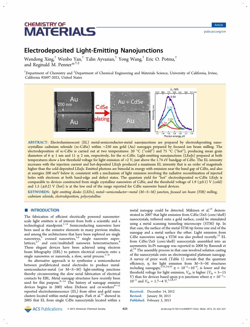
ABSTRACT: Electroluminescent (EL) metal-semiconductor-metal nanojunctions are prepared by electrodepositing nano-crystalline cadmium selenide (nc-CdSe) within ∼250 nm gold (Au) nanogaps prepared by focused ion beam milling. Theelectrodeposition of nc-CdSe is carried out at two temperatures: 20 °C (“cold”) and 75 °C (“hot”), producing mean graindiameters of 6 ± 1 nm and 11 ± 2 nm, respectively, for the nc-CdSe. Light-emitting nanojunctions (LEnJs) prepared at bothtemperatures show a low threshold voltage for light emission of <2 V; just above the 1.74 eV bandgap of CdSe. The EL intensityincreases with the injection current and hot-deposited LEnJs produced a maximum EL intensity that is an order of magnitudehigher than the cold-deposited LEnJs. Emitted photons are bimodal in energy with emission near the band gap of CdSe, and alsoat energies 200 meV below it; consistent with a mechanism of light emission involving the radiative recombination of injectedholes with electrons at both band-edge and defect states. The quantum yield for “hot” electrodeposited nc-CdSe LEnJs iscomparable to devices constructed from single crystalline nanowires of CdSe, and the threshold voltage of 1.9 (±0.1) V (cold)and 1.5 (±0.2) V (hot) is at the low end of the range reported for CdSe nanowire based devices.
KEYWORDS: light emitting diodes (LEDs), metal−semiconductor−metal (M−S−M) junction, focused ion beam (FIB) milling,cadmium selenide, electrodeposition, polycrystalline
■ INTRODUCTION
The fabrication of efficient electrically powered nanometer-scale light emitters is of interest from both a scientific and atechnological standpoint.1−4 Semiconducting nanowires havebeen used as the emissive elements in many previous studies,and among the architectures that have been explored are singlenanowires,5 crossed nanowires,1,6 single nanowire super-lattices,2,7 and core/multishell nanowire heterostructures.8
These elegant devices have been achieved using electronbeam lithography (EBL) to pattern electrical contacts onto asingle nanowires or nanorods, a slow, serial process.1−8
An alternative approach is to synthesize a semiconductorbetween prefabricated metal electrodes to produce metal-semiconductor-metal (or M−S−M) light-emitting junctionsthereby circumventing the slow serial fabrication of electricalcontacts by EBL. Metal nanogap structures have recently beenused for this purpose.9−14 The history of nanogap emissivedevices begins in 2002 when Dickson and co-workers9−11
reported electroluminescence (EL) from silver and gold nanoclusters located within metal nanogaps. Park et al.12 showed in2005 that EL from single CdSe nanocrystals located within a
metal nanogap could be detected. Makinen et al.13 demon-strated in 2007 that light emission from CdSe/ZnS (core/shell)nanocrystals, tethered onto a gold surface, could be stimulatedusing a metal scanning tunneling microscope (STM) tip. Inthat case, the surface of the metal STM tip forms one end of thenanogap and a metal surface the other. Light emission fromCdSe nanowires using a STM was also probed recently.15 ELfrom CdSe/ZnS (core/shell) nanocrystals assembled into anasymmetric In:Pt nanogap was reported in 2008 by Bawendi etal.14 The assembly process in that case involved solution castingof the nanocrystals onto an electromigrated platinum nanogap.A survey of prior work (Table 1) reveals that the quantumefficiency, η, for light emission from M−S−M structuresincluding nanogaps,5,12,14,16 η = 10−5−10−6, is lower and thethreshold voltage for light emission, Vth, is higher (Vth = 5−15V) than for devices based upon p-n junctions where η = 10−2−10−5 and Vth = 1.7−4 V.1,2,8,17
Received: December 14, 2012Revised: January 30, 2013Published: February 3, 2013
Article
pubs.acs.org/cm
© 2013 American Chemical Society 623 dx.doi.org/10.1021/cm304001f | Chem. Mater. 2013, 25, 623−631
All of the examples cited above have involved an emissiveelement composed of a single crystalline nanoparticle ornanowire, or an ensemble of single crystalline nanostructures.Electrodeposition has not been investigated as a means forselectively functionalizing metal nanogaps with emissivesemiconducting materials to our knowledge. Here wedemonstrate a simple, high-throughput method for preparingnanoscale M−S−M LEnJs that exploits the electrodeposition ofnanocrystalline CdSe (nc-CdSe) into gold nanogap structures.These nanogaps are produced by focused ion beam (FIB)milling18 which produces uniform and reproducible nanogapshaving widths of 200−250 nm in evaporated gold films.Cadmium selenide was selected as the emissive material bothbecause stoichiometric nc-CdSe can be electrodeposited19−23
and because it has a direct bandgap at 1.74 eV.24 Previously, wehave electrodeposited nc-CdSe to produce photoconductivenanogaps,25 nanowire arrays for photodetectors,22,26,27 andfield-effect transistors.28 In that work, we found that nc-CdSeelectroplated at room temperature (Tdep = 20 °C) had a averagegrain diameter of ≈5 nm, a high electrical resistivity, and a shortminority carrier lifetime which we attribute to an abundance ofdefect and surface states in this material.22,25−27 Electro-depositing the nc-CdSe from hot solution (Tdep = 75 °C)increases the grain diameter by a factor of two, enhancing thecarrier mobility and the electronic conductivity of thematerial.25,27 In this paper, we examine the properties ofLEnJs prepared using nc-CdSe deposited both at 20 and 75 °C.The properties of nc-CdSe are ideal for the fabrication of fastphotodetectors, but the high defect density of these materialsare not optimal for making efficient light-emitting devices.Nevertheless, the LEnJs described here are characterized by aquantum efficiency for EL, η, ranging from 1.2(±0.4) × 10−6
(cold) to 1.8(±0.7) × 10−6 (hot), values that approach the ηfor single crystalline CdSe nanowires (η = 10−5−10−6) insymmetrical M−S−M devices (Table 1).5,12 In addition, weobserve a voltage threshold for light emission, Vth, of 1.9(±0.1)V (cold) and 1.5(±0.2) V (hot) that is at the low end of therange reported for CdSe nanowire based devices (Vth ≈ 1.7−5V)5,12
■ EXPERIMENTAL SECTIONChemicals and Materials. Cadmium sulfate (CdSO4·8H2O, 98+
%), selenium oxide (SeO2, 99.9+%), iodine (I2, 99.8+%), and
chromium etchant were used as received from Sigma-Aldrich. Sulfuricacid (ULTREX ultrapure) was purchased from J. T. Baker. Potassiumiodide (KI, 99%) and acetone were used as received from Fisher (ACSCertified). Positive photoresist (Shipley, S1808) and developer(Shipley, MF-319) were purchased from Microchem Corporation.Gold pellets (5N purity, ESPI Metals) and chromium powder (3Npurity, American Elements) were used for the evaporation of films.
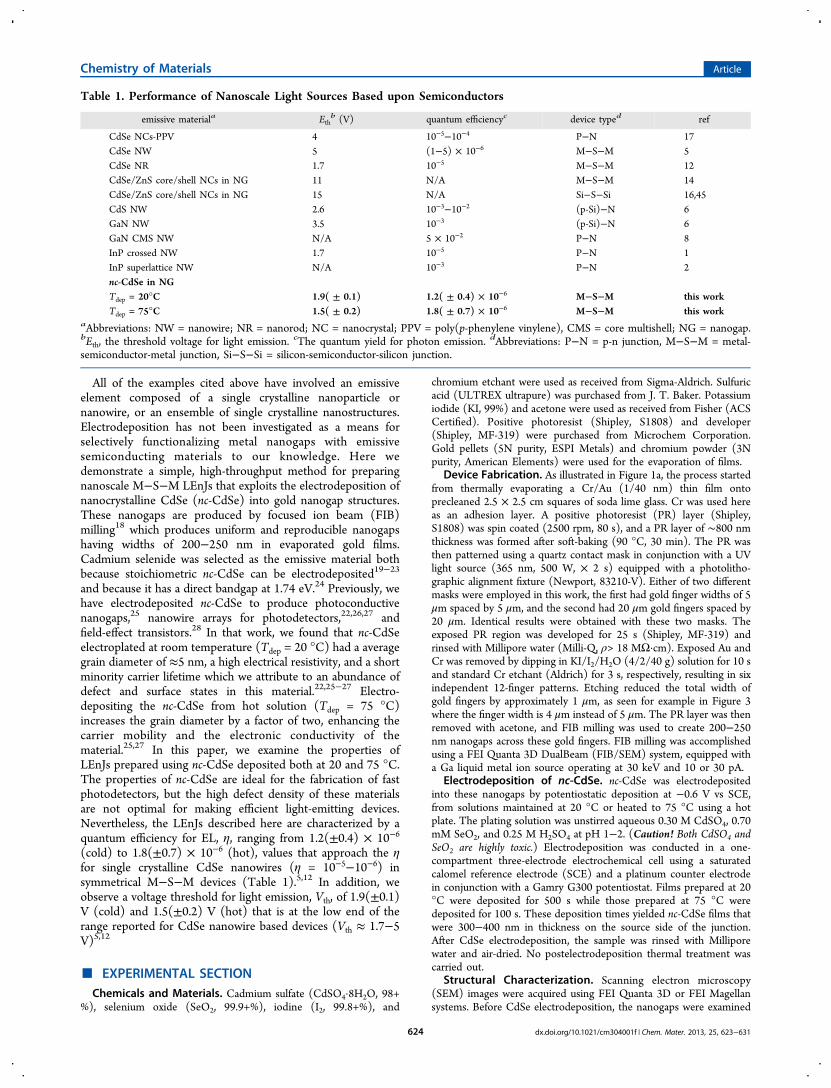
Device Fabrication. As illustrated in Figure 1a, the process startedfrom thermally evaporating a Cr/Au (1/40 nm) thin film ontoprecleaned 2.5 × 2.5 cm squares of soda lime glass. Cr was used hereas an adhesion layer. A positive photoresist (PR) layer (Shipley,S1808) was spin coated (2500 rpm, 80 s), and a PR layer of ∼800 nmthickness was formed after soft-baking (90 °C, 30 min). The PR wasthen patterned using a quartz contact mask in conjunction with a UVlight source (365 nm, 500 W, × 2 s) equipped with a photolitho-graphic alignment fixture (Newport, 83210-V). Either of two differentmasks were employed in this work, the first had gold finger widths of 5μm spaced by 5 μm, and the second had 20 μm gold fingers spaced by20 μm. Identical results were obtained with these two masks. Theexposed PR region was developed for 25 s (Shipley, MF-319) andrinsed with Millipore water (Milli-Q, ρ> 18 MΩ·cm). Exposed Au andCr was removed by dipping in KI/I2/H2O (4/2/40 g) solution for 10 sand standard Cr etchant (Aldrich) for 3 s, respectively, resulting in sixindependent 12-finger patterns. Etching reduced the total width ofgold fingers by approximately 1 μm, as seen for example in Figure 3where the finger width is 4 μm instead of 5 μm. The PR layer was thenremoved with acetone, and FIB milling was used to create 200−250nm nanogaps across these gold fingers. FIB milling was accomplishedusing a FEI Quanta 3D DualBeam (FIB/SEM) system, equipped witha Ga liquid metal ion source operating at 30 keV and 10 or 30 pA.
Electrodeposition of nc-CdSe. nc-CdSe was electrodepositedinto these nanogaps by potentiostatic deposition at −0.6 V vs SCE,from solutions maintained at 20 °C or heated to 75 °C using a hotplate. The plating solution was unstirred aqueous 0.30 M CdSO4, 0.70mM SeO2, and 0.25 M H2SO4 at pH 1−2. (Caution! Both CdSO4 andSeO2 are highly toxic.) Electrodeposition was conducted in a one-compartment three-electrode electrochemical cell using a saturatedcalomel reference electrode (SCE) and a platinum counter electrodein conjunction with a Gamry G300 potentiostat. Films prepared at 20°C were deposited for 500 s while those prepared at 75 °C weredeposited for 100 s. These deposition times yielded nc-CdSe films thatwere 300−400 nm in thickness on the source side of the junction.After CdSe electrodeposition, the sample was rinsed with Milliporewater and air-dried. No postelectrodeposition thermal treatment wascarried out.
Structural Characterization. Scanning electron microscopy(SEM) images were acquired using FEI Quanta 3D or FEI Magellansystems. Before CdSe electrodeposition, the nanogaps were examined
Table 1. Performance of Nanoscale Light Sources Based upon Semiconductors
emissive materiala Ethb (V) quantum efficiencyc device typed ref
CdSe NCs-PPV 4 10−5−10−4 P−N 17CdSe NW 5 (1−5) × 10−6 M−S−M 5CdSe NR 1.7 10−5 M−S−M 12CdSe/ZnS core/shell NCs in NG 11 N/A M−S−M 14CdSe/ZnS core/shell NCs in NG 15 N/A Si−S−Si 16,45CdS NW 2.6 10−3−10−2 (p-Si)−N 6GaN NW 3.5 10−3 (p-Si)−N 6GaN CMS NW N/A 5 × 10⁻² P−N 8InP crossed NW 1.7 10−5 P−N 1InP superlattice NW N/A 10−3 P−N 2nc-CdSe in NGTdep = 20°C 1.9( ± 0.1) 1.2( ± 0.4) × 10−6 M−S−M this workTdep = 75°C 1.5( ± 0.2) 1.8( ± 0.7) × 10−6 M−S−M this work
aAbbreviations: NW = nanowire; NR = nanorod; NC = nanocrystal; PPV = poly(p-phenylene vinylene), CMS = core multishell; NG = nanogap.bEth, the threshold voltage for light emission. cThe quantum yield for photon emission. dAbbreviations: P−N = p-n junction, M−S−M = metal-semiconductor-metal junction, Si−S−Si = silicon-semiconductor-silicon junction.
Chemistry of Materials Article
dx.doi.org/10.1021/cm304001f | Chem. Mater. 2013, 25, 623−631624
at an accelerating voltage of 5 keV without metal coating. Afterdeposition, the sample was reexamined at 10 keV after plasma coatingwith Au/Pd to ameliorate charging. EDX spectra were collected on anFEI Quanta 3D equipped with a 50 mm2 silicon drift X-ray detector(Oxford instruments, X-MAX).Grazing-incidence X-ray diffraction (GIXRD) patterns were
obtained using a Rigaku Smartlab X-ray diffractometer employingthe parallel beam optics (PB/PSA) with a fixed incident angle of 0.3°.The X-ray generator was operated at 40 kV and 44 mA with Cu Kα
irradiation. The integrated Rigaku PDXL X-ray pattern data processingsoftware was used to analyze acquired patterns and estimate the meangrain diameter.Transmission electron microscopy (TEM) images and selective area
electron diffraction (SAED) patterns were obtained using a PhilipsCM-20 TEM operating at 200 keV. An SAED aperture of 2.5 μm wasused, and the diameter of the selected specimen area was ∼100 nm.Samples for TEM analysis were prepared by patterning the nc-CdSe-filled gold nanogap on top of a 10 nm thick Si3N4 membrane windowcentered on a 200 μm thick silicon frame (Norcada Inc.).Characterization of EL Emission. EL measurements were carried
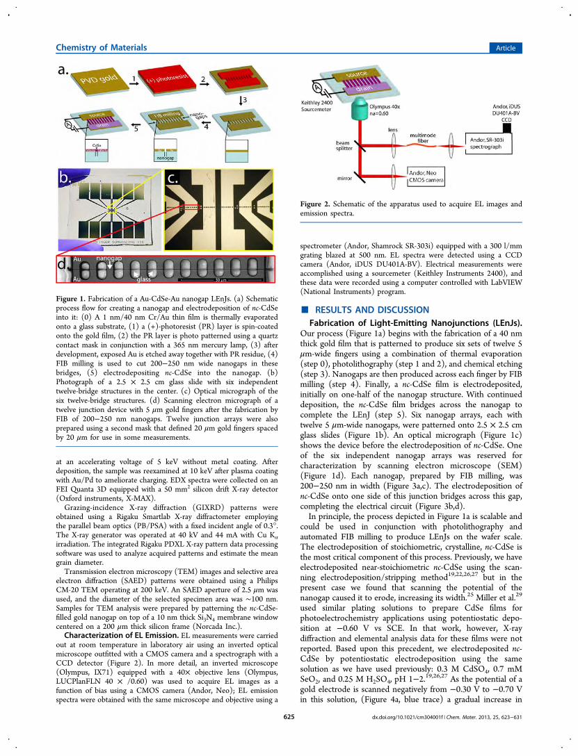
out at room temperature in laboratory air using an inverted opticalmicroscope outfitted with a CMOS camera and a spectrograph with aCCD detector (Figure 2). In more detail, an inverted microscope(Olympus, IX71) equipped with a 40× objective lens (Olympus,LUCPlanFLN 40 × /0.60) was used to acquire EL images as afunction of bias using a CMOS camera (Andor, Neo); EL emissionspectra were obtained with the same microscope and objective using a
spectrometer (Andor, Shamrock SR-303i) equipped with a 300 l/mmgrating blazed at 500 nm. EL spectra were detected using a CCDcamera (Andor, iDUS DU401A-BV). Electrical measurements wereaccomplished using a sourcemeter (Keithley Instruments 2400), andthese data were recorded using a computer controlled with LabVIEW(National Instruments) program.
■ RESULTS AND DISCUSSIONFabrication of Light-Emitting Nanojunctions (LEnJs).
Our process (Figure 1a) begins with the fabrication of a 40 nmthick gold film that is patterned to produce six sets of twelve 5μm-wide fingers using a combination of thermal evaporation(step 0), photolithography (step 1 and 2), and chemical etching(step 3). Nanogaps are then produced across each finger by FIBmilling (step 4). Finally, a nc-CdSe film is electrodeposited,initially on one-half of the nanogap structure. With continueddeposition, the nc-CdSe film bridges across the nanogap tocomplete the LEnJ (step 5). Six nanogap arrays, each withtwelve 5 μm-wide nanogaps, were patterned onto 2.5 × 2.5 cmglass slides (Figure 1b). An optical micrograph (Figure 1c)shows the device before the electrodeposition of nc-CdSe. Oneof the six independent nanogap arrays was reserved forcharacterization by scanning electron microscope (SEM)(Figure 1d). Each nanogap, prepared by FIB milling, was200−250 nm in width (Figure 3a,c). The electrodeposition ofnc-CdSe onto one side of this junction bridges across this gap,completing the electrical circuit (Figure 3b,d).In principle, the process depicted in Figure 1a is scalable and
could be used in conjunction with photolithography andautomated FIB milling to produce LEnJs on the wafer scale.The electrodeposition of stoichiometric, crystalline, nc-CdSe isthe most critical component of this process. Previously, we haveelectrodeposited near-stoichiometric nc-CdSe using the scan-ning electrodeposition/stripping method19,22,26,27 but in thepresent case we found that scanning the potential of thenanogap caused it to erode, increasing its width.25 Miller et al.29
used similar plating solutions to prepare CdSe films forphotoelectrochemistry applications using potentiostatic depo-sition at −0.60 V vs SCE. In that work, however, X-raydiffraction and elemental analysis data for these films were notreported. Based upon this precedent, we electrodeposited nc-CdSe by potentiostatic electrodeposition using the samesolution as we have used previously: 0.3 M CdSO4, 0.7 mMSeO2, and 0.25 M H2SO4, pH 1−2.19,26,27 As the potential of agold electrode is scanned negatively from −0.30 V to −0.70 Vin this solution, (Figure 4a, blue trace) a gradual increase in
Figure 1. Fabrication of a Au-CdSe-Au nanogap LEnJs. (a) Schematicprocess flow for creating a nanogap and electrodeposition of nc-CdSeinto it: (0) A 1 nm/40 nm Cr/Au thin film is thermally evaporatedonto a glass substrate, (1) a (+)-photoresist (PR) layer is spin-coatedonto the gold film, (2) the PR layer is photo patterned using a quartzcontact mask in conjunction with a 365 nm mercury lamp, (3) afterdevelopment, exposed Au is etched away together with PR residue, (4)FIB milling is used to cut 200−250 nm wide nanogaps in thesebridges, (5) electrodepositing nc-CdSe into the nanogap. (b)Photograph of a 2.5 × 2.5 cm glass slide with six independenttwelve-bridge structures in the center. (c) Optical micrograph of thesix twelve-bridge structures. (d) Scanning electron micrograph of atwelve junction device with 5 μm gold fingers after the fabrication byFIB of 200−250 nm nanogaps. Twelve junction arrays were alsoprepared using a second mask that defined 20 μm gold fingers spacedby 20 μm for use in some measurements.
Figure 2. Schematic of the apparatus used to acquire EL images andemission spectra.
Chemistry of Materials Article
dx.doi.org/10.1021/cm304001f | Chem. Mater. 2013, 25, 623−631625
cathodic current is observed (Figure 4a, process (i)). Threereactions occur in this potential range29,30
+ + → ++ −H SeO 4H 4e Se(s) 3H O2 3 2 (1)
+ + →+ −Cd Se(s) 2e CdSe(s)2(2)
+ + + → ++ + −Cd H SeO 4H 6e CdSe(s) 3H O22 3 2
(3)
Reactions 1 and 2, both of which have H2SeO3 directly orindirectly as a reactant, are reduced in importance relative toprocess 3 as the concentration of H2SeO3 is reduced relative tothat of Cd2+.30,29 At potentials negative of −0.70 V to −0.75 V,cathodic current associated with cadmium metal depositionaugments the current resulting from reactions 1−3 (Figure 1a,process (ii))
+ →+ −Cd 2e Cd(s)2(4)
On the subsequent positive-going scan, metallic cadmium isanodically stripped from the nascent CdSe deposit at ∼−0.45 V(Figure 1a, process (iii))
→ ++ −Cd(s) Cd 2e2(5)
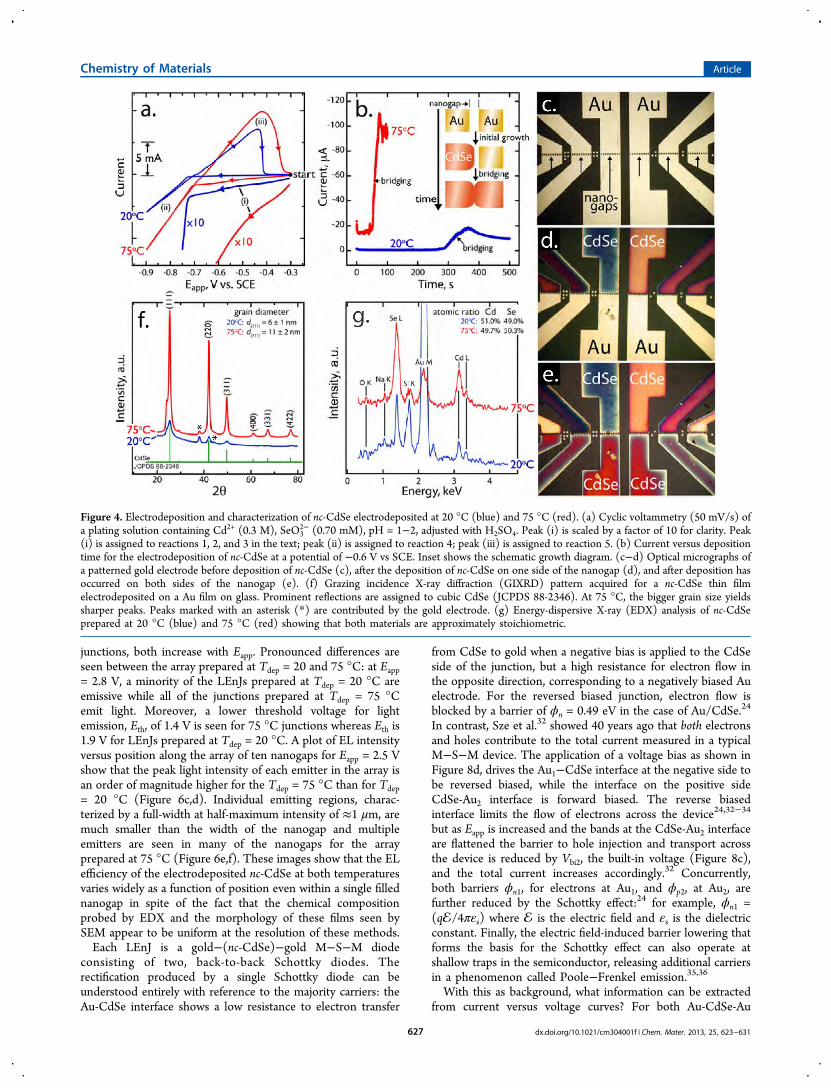
We found that stoichiometric, cubic nc-CdSe was obtained bypotentiostatic deposition at any potential in the range from−0.40 V to −0.61 V. Heating the plating solution to 75 °Cincreases the cathodic deposition current over this entirepotential range (Figure 4a, red trace), accelerating the rate ofCdSe deposition at −0.60 V by a factor of 5.To fill an array of gold nanogaps with electrodeposited nc-
CdSe, one side of the nanogap array was designated as aworking electrode, and it was electrically connected to the
potentiostat. The nanogap was then immersed into the platingsolution, and the potential was stepped from the open circuitvalue to −0.60 V. At this potential, a time-invariant steady-statedeposition current was observed within a few seconds (Figure4b). After 300 s (Tdep = 20 °C) or 50 s (75 °C), the currentrapidly increased as the nanogap filled with nc-CdSe, bridged tothe other gold contact, and the electrodeposition of nc-CdSecommenced on the initially clean side of the gold nanogap asshown schematically in the inset of Figure 4b (inset). These“bridging times” were reproducible (±5%) from device todevice in this study. nc-CdSe deposition was terminated atdeposition times that were greater than these bridging times:500 s (20°C) or 100 s (75°C). At these longer times, thedeposition current has already stabilized at the new, highersteady-state value: a signature that all twelve nanogaps in thearray were filled. These deposition times were selectedempirically because they produced identical nc-CdSe layerthicknesses of 300−400 nm in the nanogap at bothtemperatures: 20°C and 75°C. Optical micrographs of a device(Fig 4c−e) show the gold electrode before deposition (c),during the initial, steady-state deposition of nc-CdSe onto oneside of the nano gaps (d), and after the nanogap is bridged andnc-CdSe has been deposited on both sides of the nanogap (e).The variation in the color of the nc-CdSe across the device iscaused by small variations in the nc-CdSe thickness.
Cadmium Selenide Characterization. Grazing incidenceX-ray diffraction patterns (GIXRD, Figure 4f) show reflectionsthat are assignable to cubic CdSe (JCPDS 88-2346) and noreflections corresponding to either elemental cadmium orselenium. The narrower line widths seen in the pattern for nc-CdSe deposited at 75 °C is a consequence of the larger meangrain diameter for that sample as compared to nc-CdSeprepared at 20 °C. Scherrer analyses31 of the (111) or (220)reflections yields a mean grain diameter of 11 ± 2 nm and 6 ±1 nm for the 75 °C sample and the 20 °C, respectively. Ashoulder on the low angle side of the (111) reflection, seen inboth of the GIXRD patterns, shows that some hexagonal phaseis present in these predominantly cubic films (Figure 4f).Energy-dispersive X-ray spectroscopy (EDX) patterns showthat the nc-CdSe films prepared at both temperatures areapproximately stoichiometric (Figure 4g).nc-CdSe films were also investigated using TEM and SAED
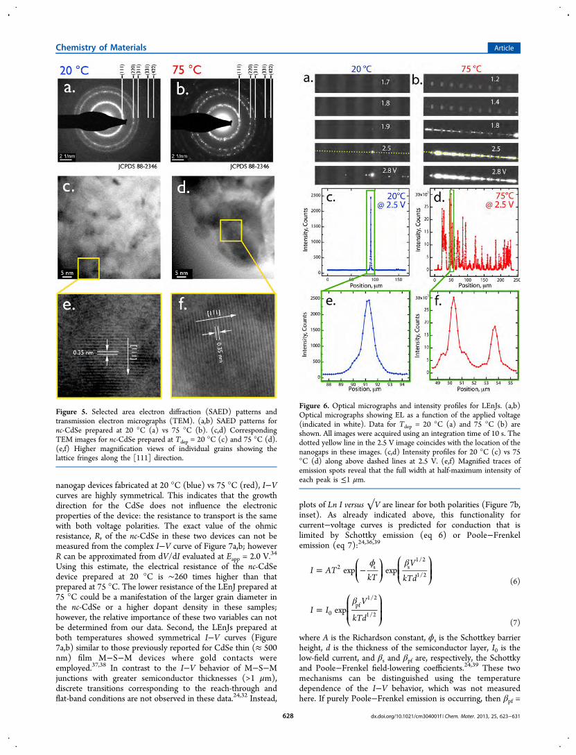
(Figure 5). SAED patterns for nc-CdSe prepared at 20 °Cconsist of diffuse, continuous diffraction rings centered at d-spacings that index to cubic CdSe (JCPDS 88-2346, Figure 5a).Since the sample diameter in this measurement was ∼100 nm(using a 2.5 μm aperture), it is apparent that these continuousrings are derived from grains that are much smaller than this. Incontrast, discontinuous rings are seen at the same d-spacings inthe SAED patterns for the samples prepared at 75 °C,indicating that a smaller number of grains are contributing todiffraction for this sample which was also ∼100 nm in diameter.We conclude that the grain diameter for the films prepared at75 °C is larger than for films prepared at the lower temperature.Lattice-resolved TEM images (Figure 5c,d) also reveal thepolycrystalline nature of the nc-CdSe deposited at bothtemperatures. At higher magnification (Figure 5e,f), latticefringes spaced by 0.35 nm are observed, corresponding to the d-spacing along the [111] lattice direction of cubic CdSe.
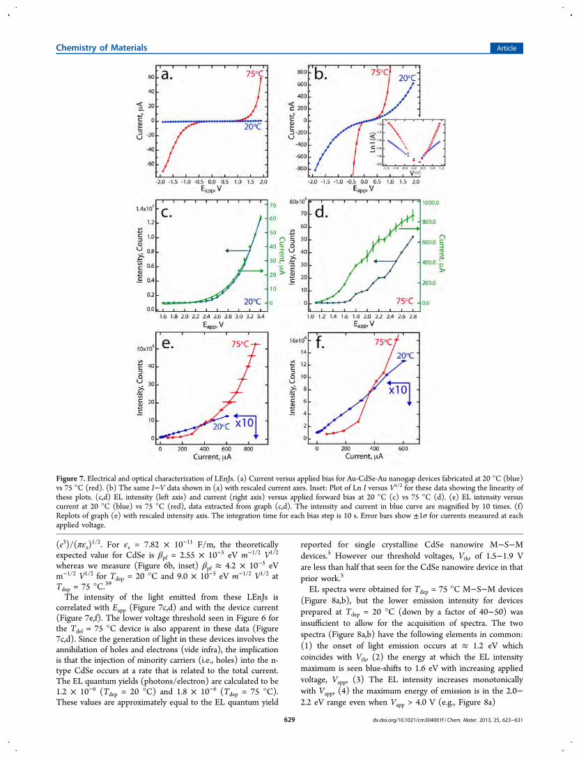
Light Emission from Nanogaps. Optical micrographs ofLEnJ arrays were recorded as a function of the applied voltagebias (Eapp, Figure 6a,b). These images show that the intensity oflight emission from LEnJs and the number of emissive
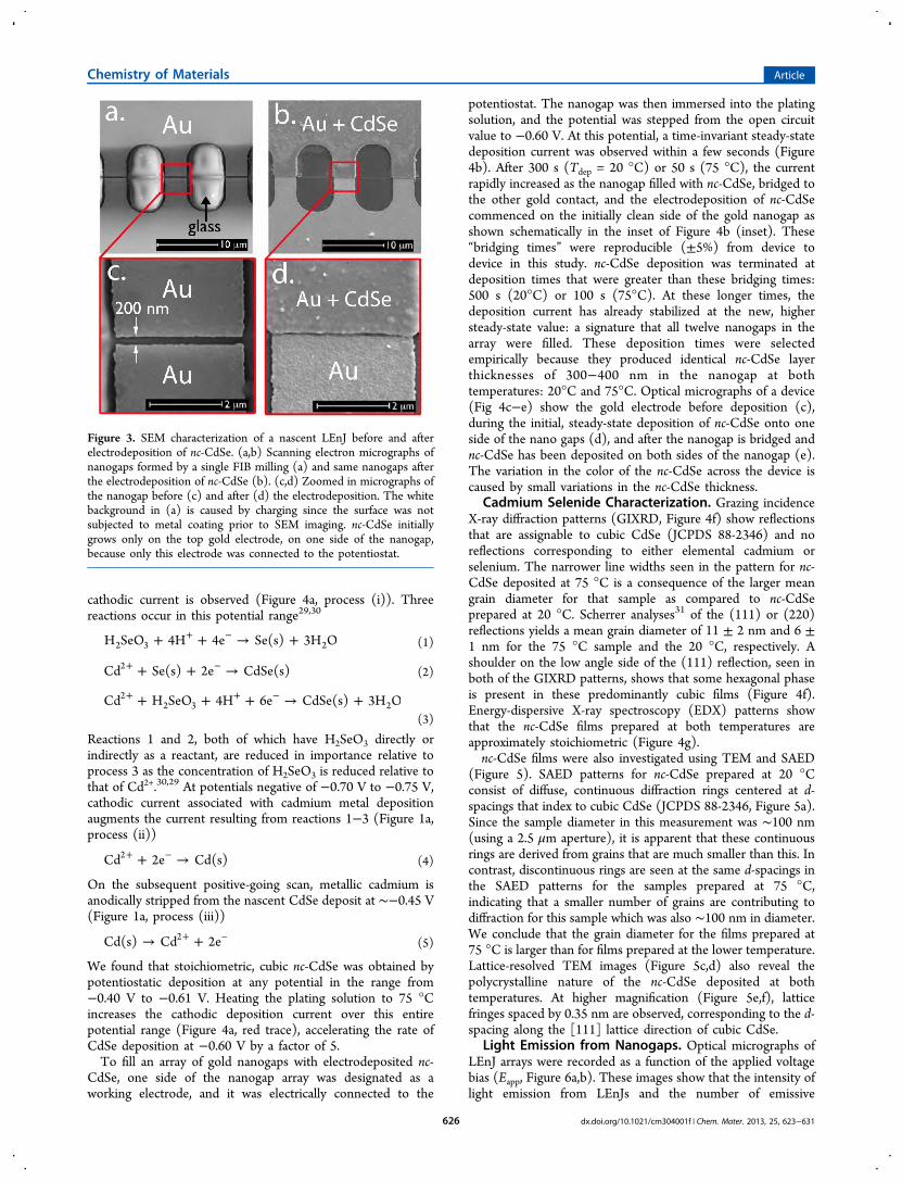
Figure 3. SEM characterization of a nascent LEnJ before and afterelectrodeposition of nc-CdSe. (a,b) Scanning electron micrographs ofnanogaps formed by a single FIB milling (a) and same nanogaps afterthe electrodeposition of nc-CdSe (b). (c,d) Zoomed in micrographs ofthe nanogap before (c) and after (d) the electrodeposition. The whitebackground in (a) is caused by charging since the surface was notsubjected to metal coating prior to SEM imaging. nc-CdSe initiallygrows only on the top gold electrode, on one side of the nanogap,because only this electrode was connected to the potentiostat.
Chemistry of Materials Article
dx.doi.org/10.1021/cm304001f | Chem. Mater. 2013, 25, 623−631626
junctions, both increase with Eapp. Pronounced differences areseen between the array prepared at Tdep = 20 and 75 °C: at Eapp= 2.8 V, a minority of the LEnJs prepared at Tdep = 20 °C areemissive while all of the junctions prepared at Tdep = 75 °Cemit light. Moreover, a lower threshold voltage for lightemission, Eth, of 1.4 V is seen for 75 °C junctions whereas Eth is1.9 V for LEnJs prepared at Tdep = 20 °C. A plot of EL intensityversus position along the array of ten nanogaps for Eapp = 2.5 Vshow that the peak light intensity of each emitter in the array isan order of magnitude higher for the Tdep = 75 °C than for Tdep= 20 °C (Figure 6c,d). Individual emitting regions, charac-terized by a full-width at half-maximum intensity of ≈1 μm, aremuch smaller than the width of the nanogap and multipleemitters are seen in many of the nanogaps for the arrayprepared at 75 °C (Figure 6e,f). These images show that the ELefficiency of the electrodeposited nc-CdSe at both temperaturesvaries widely as a function of position even within a single fillednanogap in spite of the fact that the chemical compositionprobed by EDX and the morphology of these films seen bySEM appear to be uniform at the resolution of these methods.Each LEnJ is a gold−(nc-CdSe)−gold M−S−M diode
consisting of two, back-to-back Schottky diodes. Therectification produced by a single Schottky diode can beunderstood entirely with reference to the majority carriers: theAu-CdSe interface shows a low resistance to electron transfer
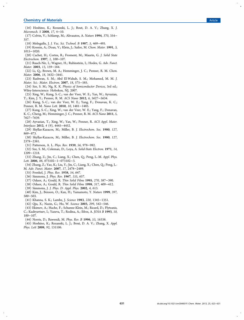
from CdSe to gold when a negative bias is applied to the CdSeside of the junction, but a high resistance for electron flow inthe opposite direction, corresponding to a negatively biased Auelectrode. For the reversed biased junction, electron flow isblocked by a barrier of ϕn = 0.49 eV in the case of Au/CdSe.24
In contrast, Sze et al.32 showed 40 years ago that both electronsand holes contribute to the total current measured in a typicalM−S−M device. The application of a voltage bias as shown inFigure 8d, drives the Au1−CdSe interface at the negative side tobe reversed biased, while the interface on the positive sideCdSe-Au2 interface is forward biased. The reverse biasedinterface limits the flow of electrons across the device24,32−34
but as Eapp is increased and the bands at the CdSe-Au2 interfaceare flattened the barrier to hole injection and transport acrossthe device is reduced by Vbi2, the built-in voltage (Figure 8c),and the total current increases accordingly.32 Concurrently,both barriers ϕn1, for electrons at Au1, and ϕp2, at Au2, arefurther reduced by the Schottky effect:24 for example, ϕn1 =(q /4πεs) where is the electric field and εs is the dielectricconstant. Finally, the electric field-induced barrier lowering thatforms the basis for the Schottky effect can also operate atshallow traps in the semiconductor, releasing additional carriersin a phenomenon called Poole−Frenkel emission.35,36With this as background, what information can be extracted
from current versus voltage curves? For both Au-CdSe-Au
Figure 4. Electrodeposition and characterization of nc-CdSe electrodeposited at 20 °C (blue) and 75 °C (red). (a) Cyclic voltammetry (50 mV/s) ofa plating solution containing Cd2+ (0.3 M), SeO3
2− (0.70 mM), pH = 1−2, adjusted with H2SO4. Peak (i) is scaled by a factor of 10 for clarity. Peak(i) is assigned to reactions 1, 2, and 3 in the text; peak (ii) is assigned to reaction 4; peak (iii) is assigned to reaction 5. (b) Current versus depositiontime for the electrodeposition of nc-CdSe at a potential of −0.6 V vs SCE. Inset shows the schematic growth diagram. (c−d) Optical micrographs ofa patterned gold electrode before deposition of nc-CdSe (c), after the deposition of nc-CdSe on one side of the nanogap (d), and after deposition hasoccurred on both sides of the nanogap (e). (f) Grazing incidence X-ray diffraction (GIXRD) pattern acquired for a nc-CdSe thin filmelectrodeposited on a Au film on glass. Prominent reflections are assigned to cubic CdSe (JCPDS 88-2346). At 75 °C, the bigger grain size yieldssharper peaks. Peaks marked with an asterisk (*) are contributed by the gold electrode. (g) Energy-dispersive X-ray (EDX) analysis of nc-CdSeprepared at 20 °C (blue) and 75 °C (red) showing that both materials are approximately stoichiometric.
Chemistry of Materials Article
dx.doi.org/10.1021/cm304001f | Chem. Mater. 2013, 25, 623−631627
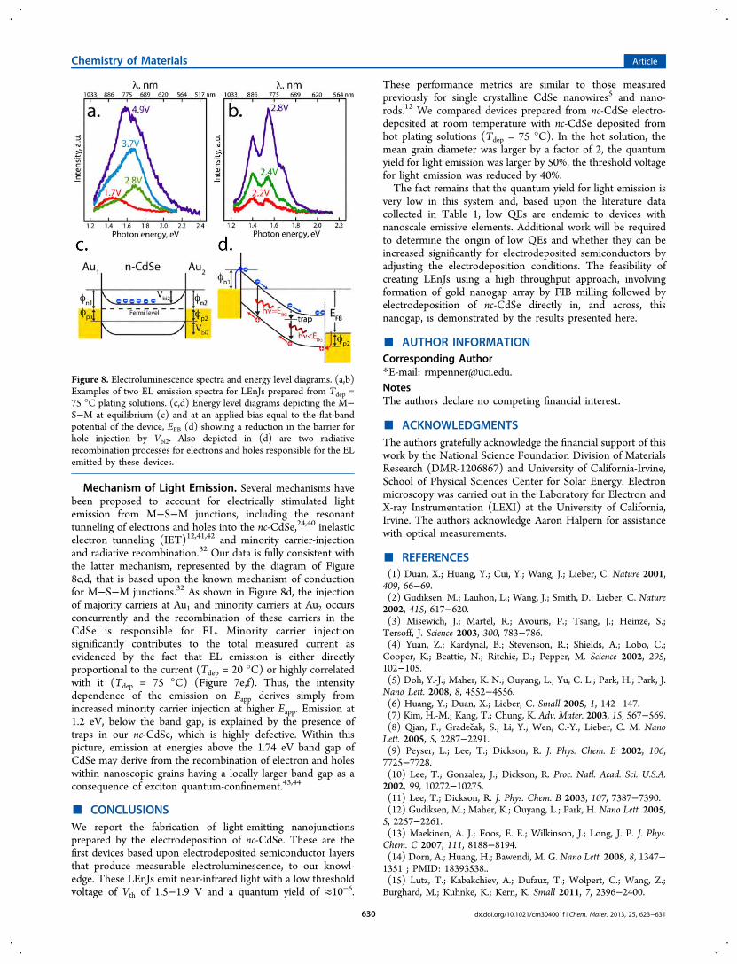
nanogap devices fabricated at 20 °C (blue) vs 75 °C (red), I−Vcurves are highly symmetrical. This indicates that the growthdirection for the CdSe does not influence the electronicproperties of the device: the resistance to transport is the samewith both voltage polarities. The exact value of the ohmicresistance, R, of the nc-CdSe in these two devices can not bemeasured from the complex I−V curve of Figure 7a,b; howeverR can be approximated from dV/dI evaluated at Eapp = 2.0 V.34
Using this estimate, the electrical resistance of the nc-CdSedevice prepared at 20 °C is ∼260 times higher than thatprepared at 75 °C. The lower resistance of the LEnJ prepared at75 °C could be a manifestation of the larger grain diameter inthe nc-CdSe or a higher dopant density in these samples;however, the relative importance of these two variables can notbe determined from our data. Second, the LEnJs prepared atboth temperatures showed symmetrical I−V curves (Figure7a,b) similar to those previously reported for CdSe thin (≈ 500nm) film M−S−M devices where gold contacts wereemployed.37,38 In contrast to the I−V behavior of M−S−Mjunctions with greater semiconductor thicknesses (>1 μm),discrete transitions corresponding to the reach-through andflat-band conditions are not observed in these data.24,32 Instead,
plots of Ln I versus √V are linear for both polarities (Figure 7b,inset). As already indicated above, this functionality forcurrent−voltage curves is predicted for conduction that islimited by Schottky emission (eq 6) or Poole−Frenkelemission (eq 7):24,36,39
ϕ β= −
⎛⎝⎜
⎞⎠⎟
⎛⎝⎜⎜
⎞⎠⎟⎟I AT
kT
V
kTdexp exp2 s s
1/2
1/2(6)
β=
⎛
⎝⎜⎜
⎞
⎠⎟⎟I I
V
kTdexp0
pf1/2
1/2(7)
where A is the Richardson constant, ϕs is the Schottkey barrierheight, d is the thickness of the semiconductor layer, I0 is thelow-field current, and βs and βpf are, respectively, the Schottkyand Poole−Frenkel field-lowering coefficients.24,39 These twomechanisms can be distinguished using the temperaturedependence of the I−V behavior, which was not measuredhere. If purely Poole−Frenkel emission is occurring, then βpf =
Figure 5. Selected area electron diffraction (SAED) patterns andtransmission electron micrographs (TEM). (a,b) SAED patterns fornc-CdSe prepared at 20 °C (a) vs 75 °C (b). (c,d) CorrespondingTEM images for nc-CdSe prepared at Tdep = 20 °C (c) and 75 °C (d).(e,f) Higher magnification views of individual grains showing thelattice fringes along the [111] direction.
Figure 6. Optical micrographs and intensity profiles for LEnJs. (a,b)Optical micrographs showing EL as a function of the applied voltage(indicated in white). Data for Tdep = 20 °C (a) and 75 °C (b) areshown. All images were acquired using an integration time of 10 s. Thedotted yellow line in the 2.5 V image coincides with the location of thenanogaps in these images. (c,d) Intensity profiles for 20 °C (c) vs 75°C (d) along above dashed lines at 2.5 V. (e,f) Magnified traces ofemission spots reveal that the full width at half-maximum intensity ofeach peak is ≤1 μm.
Chemistry of Materials Article
dx.doi.org/10.1021/cm304001f | Chem. Mater. 2013, 25, 623−631628
(e3)/(πεs)1/2. For εs = 7.82 × 10⁻¹¹ F/m, the theoretically
expected value for CdSe is βpf = 2.55 × 10⁻⁵ eV m−1/2 V1/2
whereas we measure (Figure 6b, inset) βpf ≈ 4.2 × 10⁻⁵ eVm−1/2 V1/2 for Tdep = 20 °C and 9.0 × 10⁻⁵ eV m−1/2 V1/2 atTdep = 75 °C.39
The intensity of the light emitted from these LEnJs iscorrelated with Eapp (Figure 7c,d) and with the device current(Figure 7e,f). The lower voltage threshold seen in Figure 6 forthe Tdel = 75 °C device is also apparent in these data (Figure7c,d). Since the generation of light in these devices involves theannihilation of holes and electrons (vide infra), the implicationis that the injection of minority carriers (i.e., holes) into the n-type CdSe occurs at a rate that is related to the total current.The EL quantum yields (photons/electron) are calculated to be1.2 × 10−6 (Tdep = 20 °C) and 1.8 × 10⁻⁶ (Tdep = 75 °C).These values are approximately equal to the EL quantum yield
reported for single crystalline CdSe nanowire M−S−Mdevices.5 However our threshold voltages, Vth, of 1.5−1.9 Vare less than half that seen for the CdSe nanowire device in thatprior work.5
EL spectra were obtained for Tdep = 75 °C M−S−M devices(Figure 8a,b), but the lower emission intensity for devicesprepared at Tdep = 20 °C (down by a factor of 40−50) wasinsufficient to allow for the acquisition of spectra. The twospectra (Figure 8a,b) have the following elements in common:(1) the onset of light emission occurs at ≈ 1.2 eV whichcoincides with Vth, (2) the energy at which the EL intensitymaximum is seen blue-shifts to 1.6 eV with increasing appliedvoltage, Vapp, (3) The EL intensity increases monotonicallywith Vapp, (4) the maximum energy of emission is in the 2.0−2.2 eV range even when Vapp > 4.0 V (e.g., Figure 8a)
Figure 7. Electrical and optical characterization of LEnJs. (a) Current versus applied bias for Au-CdSe-Au nanogap devices fabricated at 20 °C (blue)vs 75 °C (red). (b) The same I−V data shown in (a) with rescaled current axes. Inset: Plot of Ln I versus V1/2 for these data showing the linearity ofthese plots. (c,d) EL intensity (left axis) and current (right axis) versus applied forward bias at 20 °C (c) vs 75 °C (d). (e) EL intensity versuscurrent at 20 °C (blue) vs 75 °C (red), data extracted from graph (c,d). The intensity and current in blue curve are magnified by 10 times. (f)Replots of graph (e) with rescaled intensity axis. The integration time for each bias step is 10 s. Error bars show ±1σ for currents measured at eachapplied voltage.
Chemistry of Materials Article
dx.doi.org/10.1021/cm304001f | Chem. Mater. 2013, 25, 623−631629
Mechanism of Light Emission. Several mechanisms havebeen proposed to account for electrically stimulated lightemission from M−S−M junctions, including the resonanttunneling of electrons and holes into the nc-CdSe,24,40 inelasticelectron tunneling (IET)12,41,42 and minority carrier-injectionand radiative recombination.32 Our data is fully consistent withthe latter mechanism, represented by the diagram of Figure8c,d, that is based upon the known mechanism of conductionfor M−S−M junctions.32 As shown in Figure 8d, the injectionof majority carriers at Au1 and minority carriers at Au2 occursconcurrently and the recombination of these carriers in theCdSe is responsible for EL. Minority carrier injectionsignificantly contributes to the total measured current asevidenced by the fact that EL emission is either directlyproportional to the current (Tdep = 20 °C) or highly correlatedwith it (Tdep = 75 °C) (Figure 7e,f). Thus, the intensitydependence of the emission on Eapp derives simply fromincreased minority carrier injection at higher Eapp. Emission at1.2 eV, below the band gap, is explained by the presence oftraps in our nc-CdSe, which is highly defective. Within thispicture, emission at energies above the 1.74 eV band gap ofCdSe may derive from the recombination of electron and holeswithin nanoscopic grains having a locally larger band gap as aconsequence of exciton quantum-confinement.43,44
■ CONCLUSIONSWe report the fabrication of light-emitting nanojunctionsprepared by the electrodeposition of nc-CdSe. These are thefirst devices based upon electrodeposited semiconductor layersthat produce measurable electroluminescence, to our knowl-edge. These LEnJs emit near-infrared light with a low thresholdvoltage of Vth of 1.5−1.9 V and a quantum yield of ≈10−6.
These performance metrics are similar to those measuredpreviously for single crystalline CdSe nanowires5 and nano-rods.12 We compared devices prepared from nc-CdSe electro-deposited at room temperature with nc-CdSe deposited fromhot plating solutions (Tdep = 75 °C). In the hot solution, themean grain diameter was larger by a factor of 2, the quantumyield for light emission was larger by 50%, the threshold voltagefor light emission was reduced by 40%.The fact remains that the quantum yield for light emission is
very low in this system and, based upon the literature datacollected in Table 1, low QEs are endemic to devices withnanoscale emissive elements. Additional work will be requiredto determine the origin of low QEs and whether they can beincreased significantly for electrodeposited semiconductors byadjusting the electrodeposition conditions. The feasibility ofcreating LEnJs using a high throughput approach, involvingformation of gold nanogap array by FIB milling followed byelectrodeposition of nc-CdSe directly in, and across, thisnanogap, is demonstrated by the results presented here.
■ AUTHOR INFORMATIONCorresponding Author*E-mail: [email protected] authors declare no competing financial interest.
■ ACKNOWLEDGMENTSThe authors gratefully acknowledge the financial support of thiswork by the National Science Foundation Division of MaterialsResearch (DMR-1206867) and University of California-Irvine,School of Physical Sciences Center for Solar Energy. Electronmicroscopy was carried out in the Laboratory for Electron andX-ray Instrumentation (LEXI) at the University of California,Irvine. The authors acknowledge Aaron Halpern for assistancewith optical measurements.
■ REFERENCES(1) Duan, X.; Huang, Y.; Cui, Y.; Wang, J.; Lieber, C. Nature 2001,409, 66−69.(2) Gudiksen, M.; Lauhon, L.; Wang, J.; Smith, D.; Lieber, C. Nature2002, 415, 617−620.(3) Misewich, J.; Martel, R.; Avouris, P.; Tsang, J.; Heinze, S.;Tersoff, J. Science 2003, 300, 783−786.(4) Yuan, Z.; Kardynal, B.; Stevenson, R.; Shields, A.; Lobo, C.;Cooper, K.; Beattie, N.; Ritchie, D.; Pepper, M. Science 2002, 295,102−105.(5) Doh, Y.-J.; Maher, K. N.; Ouyang, L.; Yu, C. L.; Park, H.; Park, J.Nano Lett. 2008, 8, 4552−4556.(6) Huang, Y.; Duan, X.; Lieber, C. Small 2005, 1, 142−147.(7) Kim, H.-M.; Kang, T.; Chung, K. Adv. Mater. 2003, 15, 567−569.(8) Qian, F.; Gradecak, S.; Li, Y.; Wen, C.-Y.; Lieber, C. M. NanoLett. 2005, 5, 2287−2291.(9) Peyser, L.; Lee, T.; Dickson, R. J. Phys. Chem. B 2002, 106,7725−7728.(10) Lee, T.; Gonzalez, J.; Dickson, R. Proc. Natl. Acad. Sci. U.S.A.2002, 99, 10272−10275.(11) Lee, T.; Dickson, R. J. Phys. Chem. B 2003, 107, 7387−7390.(12) Gudiksen, M.; Maher, K.; Ouyang, L.; Park, H. Nano Lett. 2005,5, 2257−2261.(13) Maekinen, A. J.; Foos, E. E.; Wilkinson, J.; Long, J. P. J. Phys.Chem. C 2007, 111, 8188−8194.(14) Dorn, A.; Huang, H.; Bawendi, M. G. Nano Lett. 2008, 8, 1347−1351 ; PMID: 18393538..(15) Lutz, T.; Kabakchiev, A.; Dufaux, T.; Wolpert, C.; Wang, Z.;Burghard, M.; Kuhnke, K.; Kern, K. Small 2011, 7, 2396−2400.
Figure 8. Electroluminescence spectra and energy level diagrams. (a,b)Examples of two EL emission spectra for LEnJs prepared from Tdep =75 °C plating solutions. (c,d) Energy level diagrams depicting the M−S−M at equilibrium (c) and at an applied bias equal to the flat-bandpotential of the device, EFB (d) showing a reduction in the barrier forhole injection by Vbi2. Also depicted in (d) are two radiativerecombination processes for electrons and holes responsible for the ELemitted by these devices.
Chemistry of Materials Article
dx.doi.org/10.1021/cm304001f | Chem. Mater. 2013, 25, 623−631630
(16) Hoshino, K.; Rozanski, L. J.; Bout, D. A. V.; Zhang, X. J.Micromech. S 2008, 17, 4−10.(17) Colvin, V.; Schlamp, M.; Alivasatos, A. Nature 1994, 370, 354−357.(18) Melngailis, J. J. Vac. Sci. Technol. B 1987, 5, 469−495.(19) Kressin, A.; Doan, V.; Klein, J.; Sailor, M. Chem. Mater. 1991, 3,1015−1020.(20) Cachet, H.; Cortes, R.; Froment, M.; Maurin, G. J. Solid StateElectrochem. 1997, 1, 100−107.(21) Ruach-Nir, I.; Wagner, H.; Rubinstein, I.; Hodes, G. Adv. Funct.Mater. 2003, 13, 159−164.(22) Li, Q.; Brown, M. A.; Hemminger, J. C.; Penner, R. M. Chem.Mater. 2006, 18, 3432−3441.(23) Rashwan, S. M.; Abd El-Wahab, S. M.; Mohamed, M. M. J.Mater. Sci.: Mater. Electron. 2007, 18, 575−585.(24) Sze, S. M.; Ng, K. K. Physics of Semiconductor Devices, 3rd ed.;Wiley-Interscience: Hoboken, NJ, 2007.(25) Xing, W.; Kung, S.-C.; van der Veer, W. E.; Yan, W.; Ayvazian,T.; Kim, J. Y.; Penner, R. M. ACS Nano 2012, 6, 5627−5634.(26) Kung, S.-C.; van der Veer, W. E.; Yang, F.; Donavan, K. C.;Penner, R. M. Nano Lett. 2010, 10, 1481−1485.(27) Kung, S.-C.; Xing, W.; van der Veer, W. E.; Yang, F.; Donavan,K. C.; Cheng, M.; Hemminger, J. C.; Penner, R. M. ACS Nano 2011, 5,7627−7639.(28) Ayvazian, T.; Xing, W.; Yan, W.; Penner, R. ACS Appl. Mater.Interfaces 2012, 4 (9), 4445−4452.(29) Skyllas-Kazacos, M.; Miller, B. J. Electrochem. Soc. 1980, 127,869−873.(30) Skyllas-Kazacos, M.; Miller, B. J. Electrochem. Soc. 1980, 127,2378−2381.(31) Patterson, A. L. Phys. Rev. 1939, 56, 978−982.(32) Sze, S. M.; Coleman, D.; Loya, A. Solid-State Electron. 1971, 14,1209−1218.(33) Zhang, Z.; Jin, C.; Liang, X.; Chen, Q.; Peng, L.-M. Appl. Phys.Lett. 2006, 88, 073102−1−073102−3.(34) Zhang, Z.; Yao, K.; Liu, Y.; Jin, C.; Liang, X.; Chen, Q.; Peng, L.-M. Adv. Funct. Mater. 2007, 17, 2478−2489.(35) Frenkel, J. Phys. Rev. 1938, 54, 647.(36) Simmons, J. Phys. Rev. 1967, 155, 657.(37) Oduor, A.; Gould, R. Thin Solid Films 1995, 270, 387−390.(38) Oduor, A.; Gould, R. Thin Solid Films 1998, 317, 409−412.(39) Simmons, J. J. Phys. D: Appl. Phys. 2002, 4, 613.(40) Kim, J.; Benson, O.; Kan, H.; Yamamoto, Y. Nature 1999, 397,500−503.(41) Khanna, S. K.; Lambe, J. Science 1983, 220, 1345−1351.(42) Qiu, X.; Nazin, G.; Ho, W. Science 2003, 299, 542−546.(43) Ekimov, A.; Hache, F.; Schanne-Klein, M.; Ricard, D.; Flytzanis,C.; Kudryavtsev, I.; Yazeva, T.; Rodina, A.; Efros, A. JOSA B 1993, 10,100−107.(44) Norris, D.; Bawendi, M. Phys. Rev. B 1996, 53, 16338.(45) Hoshino, K.; Rozanski, L. J.; Bout, D. A. V.; Zhang, X. Appl.Phys. Lett 2008, 92, 131106.
Chemistry of Materials Article
dx.doi.org/10.1021/cm304001f | Chem. Mater. 2013, 25, 623−631631