Embed Size (px)
Citation preview

PROCEEDINGS OF THE IEEE. VOL 57. NO. 9. SEPTEMBER 1969 1587
Electromigration Failure Modes in Aluminum Metallization for Semiconductor Devices
Abstract-Two wear-out type failure modes involving aluminum metallization for semiconductor devices are described. Both modes involve mass transport by momentum exchange between conducting electrons and metal ions. The first failure mode is the formation of an electrically open circuit due to the condensation of vacancies in the aluminum to form voids. The second is the formation of etch pits into silicon by the dissolution of silicon into aluminum, and the transport of the solute ions down the aluminum conductor away from the silicon-aluminum interface by electron wind forces. The process continues until an etch pit grows into the silicon to a depth sufficient to short out an underlying junction.
E I. INTRODUCTION
LECTROMIGRATION is a term applied to the transport of mass in metals when stressed at high current densities. Recently, it has been identified as
the cause of two distinct wear-out failure modes for silicon components employing aluminum as a metallization mate- rial. One failure mode is the formation of an open circuit in an aluminum conductor due to void formation by the con- densation of vacancies in the aluminum. The second is the growth of etch pits into silicon, at ohmic contacts where electrons leave the silicon and enter aluminum, by the solid- state dissolution of silicon into aluminum and the transport of the solute ions down the aluminum conductor away from the silicon-aluminum interface. The process continues until an etch pit grows into the silicon to a depth sufficient to short out an underlying junction.
Electromigration has been known for several decades, being observed in both molten and solid metals [1]-[3]. During the present decade Huntington and his co-workers at the Rensselaer Polytechnic Institute have contributed greatly to an understanding of the processes involved by the study of the motion of surface scratches on bulk metals [4]-[ll]. Much, however, is still not well understood about the processes involved, especially in the cases of complex metals and solute ions. Recently, with the recognition that electromigration can lead to failures in semiconductor de- vices, several studies have been reported on mass transport in thin metal films [12]-[22].
Both failure modes of silicon devices contacted by alumi- num due to electromigration are described in the following sections. Equations are developed which enable prediction of the lifetime of aluminum film conductors stressed at
Manuscript received February 19, 1969; revised March 10, 1969. This work was supported in part by the Rome Air Development Center, Air Force Systems Command, Grif f iss Air Force Base, New York, N. Y., under Contract F30602-67-C-0166, Project 5519.
The author is with Motorola, Inc., Semiconductor Products Division, Phoenix. Ariz.
Fig. 1. 1 mil wide AI stripe I/C conductor which has failed due to electromigration.
high current densities. Only a qualitative description of the etch pit type of failure mode is presented at this time.
11. ALUMINUM FILM CONDUCTOR FAILURE BY ELECTROMIGRATION
A scanning electron microscope photomicrograph (SEM) of an aluminum film conductor of an integrated circuit which has failed due to electromigration processes is shown in Fig. 1. Several voids in the 1 mil wide aluminum stripe are seen, with one void extending across the entire conduc- tor and resulting in an open circuit.
In the study of mass transport in bulk metals it has been concluded that a metal ion which has been thermally ac- tivated and is at a saddle point (lifted out of its potential well and is essentially free of the metal lattice) is acted on by two forces in an electrically conducting single band metal [41-[111:
1 ) The electric field applied to the conductor will exert a force on the activated positive ion in a direction o p posite to the electron flow.
2) The rate of momentum exchange between the con- ducting electrons colliding with the activated metal
Authorized licensed use limited to: PORTLAND STATE UNIVERSITY. Downloaded on March 29, 2009 at 03:40 from IEEE Xplore. Restrictions apply.

1588
ions will exert a force on the metal ion in the direction of electron flow.
Because of shielding electrons the force on the ion due to the electric field is quite small; therefore, the predominating force is that of the “electron wind.” As a result, activated metal ions which are upstream (in terms of electron flow) from a vacancy have a higher probability of occupying the vacancy site than do other near neighbor ions which sur- round the vacancy. Metal ions travel therefore toward the positive end of the conductor while vacancies move toward the negative end. The vacancies condense to form voids while the ions condense at certain discontinuities to form crystals, whiskers, and nondescript hillocks. Surface scratch marks on bulk metal conductors behave as vacancies and are observed to move along the surface of the conductor in the direction of the negative terminal. The activation energy for the velocity of surface scratch motion on bulk materials was determined to be identical to the activation energy for the lattice self-diffusion of the metals [4k[11].
A . Simple Theory If the electrons at zero field are considered to have an
entirely random motion, both before and after being ac- celerated and colliding with ions with nearly elastic col- lisions,’ they impart all of their momentum to the ions. The rate of mass transport by momentum transfer between thermally activated ions and the electrons is directly pro- portional to the number of activated ions or “targets” available per cm3, the number of electrons per second available for striking the activated ions, and the momentum of these electrons. This may be expressed as :
R = F x (electron momentum) x (number of electrons passing through a unit vol-
ume per second) (1) x (effective target cross section) x (aluminum activated ion density)
where R is the rate of mass transport and F is a constant. The additional momentum P picked up by an electron
falling through an electric field a distance of its mean free path I, with an average velocity u, is
1 1 P = eE - = epJ- = eEz = epJ7 (2)
The average velocity u is determined mainly by the ther- mal velocity uT and is perturbed only slightly by the drift velocity ud. T is the mean free time between collisions, e is the charge on an electron, p is the volume resistivity, and J the current density.
The number of electrons per second which are trans- ported through a unit volume of metal is related to J by
u v
N = nud = J/e (3)
where n is the electron density.
The energy picked up by the electron from the field and delivered to the ions is small compared to the thermal energy.
PROCEEDINGS OF THE IEEE, SEPTEMBER 1969
One may consider the number of activated ions per cubic centimeter in the metal to follow the Arrhenius equation as a function of temperature. Thus,
Activated aluminum ion density = F,e-“#‘”kT’ (4)
where
q5 = the activation energy in electron volts, k = Boltzmann’s constant 8.62 x eV/K. T = film temperature in degrees Kelvin, and
F , =a constant for a given metal and diffusion process.
The median-time-to-failure in hours (MTF) of a metal film conductor is related to rate of mass transfer and the con- ductor cross sectional area by
F,wt R=- MTF
where F , is a constant, w is the conductor width expressed as centimeters, and t is the film thickness expressed as centi- meters. The film cross sectional area enters directly into this expression since it determines the minimum void size which must form to cause an open circuit.,
Equation (1) may be rewritten by substituting (2)-(5) as
- MTF wtF, = F(epJ i ) ( $ ~ r ) ( F ~ e - ( ~ / ~ ~ )
where o= ionic scattering cross section. The first term in parenthesis on the right-hand side of this last equation is the force acting between conducting electrons and the ions, while the second term expresses the density of the activated ions as a function of temperature. This equation neglects the opposing force due to the electric field. By con- solidation of the constants
wt q5 - = AJ2 exp. - - MTF kT
The constant A embodies several physical properties in- cluding
the volume resistivity of the metal the electron-free time between collisions or the elec- tron free path and average velocity the effective ionic scattering cross section for electrons the frequency factor for selfdiffusion of aluminum in aluminum a factor relating rate of mass transport with mean- time-to-failure.
Based upon the above analysis, an experiment was de- signed to study the failure rate of long thin aluminum film conductor stripes stressed at various current densities and temperatures. Since the aluminum films were formed by the condensation of vapor in a vacuum ambient, it was antic-
Experiments designed to test the effect of conductor cross sectional area on the life of a conductor are presented in [18].
Authorized licensed use limited to: PORTLAND STATE UNIVERSITY. Downloaded on March 29, 2009 at 03:40 from IEEE Xplore. Restrictions apply.

BLACK: ELECTROMIGRATION FAILURE MODES IN ALUMINUM METALLIZATION 1589
++ Fig. 2. Median-time-to-failure for aluminum film conductors as a function of current density, temperature, and cross sectional dimensions.
ipated that the activation energy for the failure mode would be less than that of bulk aluminum and dependent upon the degree of crystalline order of the film.
Highly polycrystalline films formed by vacuum deposi- tion onto cold substrates were suspected of exhibiting very low activation energies due to grain-boundary diffusion and surface diffusion. Well ordered films deposited on heated substrates and possessing large area .crystallites should ex- hibit a moderate activation energy for the failure mode, being depressed from the activation energy due to lattice diffusion value mainly by surface diffusion. Films de- posited with high crystalline order and coated with a glass film to reduce surface diffusion effects should possess an activation energy for this failure mode approaching that for the lattice self-diffusion of aluminum (1.4 eV) [23], [24].
From (7) it would be expected that a plot of In (wt/J2 MTF) versus (l/T°K) would be a straight line if the factors which contribute to A are slowly varying func- tions of T. The activation energy derived from the slope of this line would also be expected to be less than 1.4 eV due to the large surface-to-volume ratio and the generally small crystalline size of condensed aluminum films. In addition,
this activation energy should serve as a quality figure re- lating to the degree of perfection of evaporated films.
B. Small Crystallite Aluminum Film Experiment An experiment was designed to determine the values of
C#I and A for highly polycrystalline aluminum films. These were deposited in a high vacuum at the low Torr pres- sure range by the evaporation of 99.999 percent aluminum from tungsten filaments on a cold (< 100°C) substrate. The crystallite lateral size was about 1.2 microns. The substrate consists of 9000 A of S O z on silicon wafers. The films were etched to form conductor paths 54 x 0.5 mil x 7000 A thick, and mounted into TO-5 headers. These were wire- bonded using 0.001-inch diameter aluminum wire, and encapsulated in a dry nitrogen ambient. Each cell consisted of 10 devices from which the mean-time-to-failure was de- termined. The current density varied from 0.5 to 2.88 x lo6 A/cmZ and the mean-time-to-failure ranged from 1.5 to 850 hours.
A plot of In (wr/J2 MTF) versus (l/T°K) is presented in Fig. 2. For this experiment, film temperatures varied from
Authorized licensed use limited to: PORTLAND STATE UNIVERSITY. Downloaded on March 29, 2009 at 03:40 from IEEE Xplore. Restrictions apply.

1590 PROCEEDINGS OF THE IEEE, SEPTEMBER 1969
109°C to 260"C, corresponding to a ratio of 1.4 to 1 on the Kelvin scale. The equation representing this line is
(wt /J2 MTF) = 2.43 x 10- l6 exp - (0.48/kT) (8)
The activation energy of 0.48 eV is 34 percent of that re- ported for the lattice self-diffusion of aluminum in alumi- num of 1.4 eV.
Voids growing in such a highly stressed small grained film are shown in the scanning electron micrograph (SEM) of Fig. 1. Here, both grain boundary and surface diffusion appear to be the predominant transport mechanisms.
C . Large Crystallite Aluminum Film Experiment A similar experiment was performed to determine the life
of well ordered aluminum film conductors containing large crystallites. Deposition methods were the same as before, except that large crystallites (approximately 8 microns lateral geometry) were obtained by maintaining the sub- strate temperature at 400°C during the deposition. The film thickness was 6000 A and the line width was in excess of 0.6 mil. The cells were stressed at current densities ranging from 0.55 to 2.02 x lo6 A/cm2 and the mean-time-to-failures ranged from 12 to 1125 hours. The data for this film struc- ture are plotted in Fig. 2 as crosses. Here,
(wt /J2 MTF) = 5 x 10- l 3 exp -(0.84/kT) (9)
The increaie in activation energy to 0.84 eV for this failure mode for the large crystal well ordered films is at- tributed to the reduction of grain boundaries with their associated high self-diffusion coefficient.
Fig. 3 is an SEM of a typical large grained film after stress and shows the growth of hillocks out of the surface. Surface diffusion appears to be a predominant transport mechanism since the large area voids which form are not associated with the grain boundaries. In addition, it is seen that voids grow from the top surface, indicating that surface diffusion predominates.
D. Large Crystallite Aluminum Films With a Glass Film Overcoat
Large crystallite aluminum films were prepared with an overcoat of silica glass deposited by the vawr plating tech- nique to a thickness of 7000 A in an attempt to reduce sur- face diffusion. These aluminum films were 12 200 A thick and possessed a width of 1.46 mils. The current density for the cells varied from 0.46 to 0.908 x lo6. A/cm2 and the mean-time-to-failure ranged from 395 to a predicted 16 OOO hours. This experiment was terminated with three of the six cells exhibiting greater than 50 percent failures (3900 hours). Predicted lifetime was based upon Poisson's distribution of those films which have been aged but did not reach the 50 percent failure time.
Fig. 2 presents these data (triangular points). Here,
(wt /J2 MTF) = 8.5 x lO-''exp -(1.2/kT) (10)
The activation energy of 1.2 eV for these thick, wide, well ordered and glassed films approaches 1.4 eV, which is the
Fig. 3. Void and hillock growth in a f mil wide large grain aluminum film.
Fig. 4. Hillock growth in large grain AI film with a glass film overcoat.
activation energy for selfdiffusion of aluminum in bulk aluminum. The increase in activation energy for these films over well ordered nonglassed films is attributed to the reduction in surface diffusion due to the overlaying glass film. Also, because of its increased thickness, these films are probably better ordered than were the thinner nonglassed films.
Fig. 4 shows an SEM of a hillock which has broken through the glass overlay. The broken glass film remains in- tact, indicating that the hillock grows from the base. Void formations in these samples appear similar to those ex- hibited by the large crystal nonglassed films.
The experimental data of Fig. 2 show that these curves intersect at a temperature near 275°C. At this temperature and above, lattice diffusion predominates over surface and grain boundary diffusion; thus structural effects are not important. At temperatures lower than 275"C, however, orders of magnitude improvement in lifetime can be ob-
Authorized licensed use limited to: PORTLAND STATE UNIVERSITY. Downloaded on March 29, 2009 at 03:40 from IEEE Xplore. Restrictions apply.

BLACK: ELECTROMIGRATION FAILURE MODES IN ALUMINUM METALLIZATION 1591
tained through the use of well ordered large grained films, especially when covered with a glass film.
An accurate determination of the power for J cannot be made on the basis of this present experiment because of small errors in the measurement of film temperature. A sta- tistical analysis of the data does indicate that the exponent of J exceeds the value of 2 by only a slight amount. At this time and for the current density range of this experiment, the exponent value of 2 for J appears valid.
111. THE EFFECT OF GRADIENTS ON CONDUCTOR LIFETIME
In the above discussion, it was assumed that there were no gradients of temperature, current density, or ion diffusion coefficient. If gradients exist, as defined in Fig. 5 , it would be expected that hillocks and voids would preferentially grow at the positions indicated. This is because aluminum ions in the plateau moving to the right arrive at the negative gradient faster than they are removed from that region. The aluminum ions accumulate in this region and form crystals, whiskers, or nondescript extruded-appearing- formations just upstream (in terms of electron flow) from a negative gradient.
In a similar manner, aluminum ions just downsteam from a positive gradient are removed from that region faster than they are replaced by ions from further upstream. The resul- tant excess vacancies condense at that point to form voids. Finally, voids and whiskers form more slowly in gradient- free regions because vacancies generated by ions flowing downstream are readily filled by ions moving from upstream portions of the conductor.
Films containing positive gradients of temperature, cur- rent density, or ion diffusion coefficient would be expected to fail earlier than predicted by @)-(lo). This is due to the formation of voids which quickly lead to an open circuit. To test qualitatively the effect of gradients in conductor ion diffusion on conductor lifetime, test vehicles were made in which the conductor ‘material composition was changed abruptly. This was done by contacting resistors diffused into silicon with aluminum conductors. The diffused resis- tors are silicon doped with a p-type impurity, and are typi- cal of those used in silicon integrated circuits.
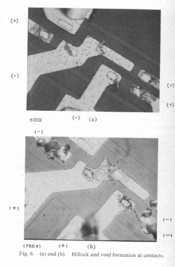
Several arrays of three test resistors were evaluated by stressing the aluminum for 140 hours at current densities of 1.3 x lo5 A/cm2 and conductor temperatures of 235°C. Fig. 6(a) shows a set of resistors after aging at the above conditions. Whiskers and hillocks grow (out of focus) from the negative resistor contact regions while voids develop at the positive resistor terminals. All samples tested displayed this effect, ruling out possible contact resistance and ther- mal effects.
A second set of similar resistors, stressed in a like manner except for a reverse in polarity, at the contacts is shown in Fig. 6(b). Again, hillocks and whiskers form at the negative terminals and voids form near the positive resistor terminals as predicted.
The SEM photomicrograph of Fig. 7 shows extensive
t TEMPERATURE,
CURRENT DENSITY
OR DIFFUSION COEFFICIENT
(+>
(- 1
I GRADIENT NEGATIVE GRADIENT
CONDUCTOR LENGTH +
ELECTRON FLOW 4
Fig. 5 . Definition of gradients.
(-1
I-)
(750x1 ( + I (b) Fig. 6. (a) and (b). Hillock and void formation at contacts.
whisker growth at the negative terminals of two of these resistors. One whisker is nearly 5.5 mils long. Here the “hillocks” appear to be extruded from the aluminum film surface. The relative heights of the aluminum film and of the hillocks indicate extensive mass transport of the alumi- num to these regions.
An SEM photomicrograph of the positive terminals of the resistors is shown in Fig. 8. At these terminals electrons leave the silicon and enter the aluminum. The depletion of the aluminum formed a void which resulted in an open cir- cuit, as indicated. The position of this void is located just
Authorized licensed use limited to: PORTLAND STATE UNIVERSITY. Downloaded on March 29, 2009 at 03:40 from IEEE Xplore. Restrictions apply.
1592 PROCEEDINGS OF THE IEEE, SEPTEMBER 1969
Fig. 7. Detail of hillock and whisker growth at negative resistor contacts.
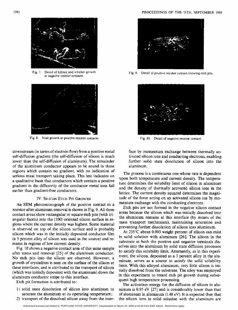
Fig. 9. Detail of positive resistor contact showing etch pits.
Fig. 8. Void growth at positive resistor contacts. Fig. 10. Detail of negative resistor contact.
downstream (in terms of electron flow) from a positive metal self-diffusion gradient (the self-diffusion of silicon is much lower than the self-diffusion of aluminum). The remainder of the aluminum conductor appears to be sound in those regions which contain no gradient, with no indication of serious mass transport taking place. This test indicates on a qualitative basis that conductors which contain a positive gradient in the diffusivity of the conductor metal ions fail earlier than gradient-free conductors.
IV. SILICON ETCH PIT GROWTH An SEM photomicrograph of the positive contact to a
resistor after aluminum removal is shown in Fig. 9. All three contact areas show rectangular or square etch pits (with tri- angular facets) into the (100) oriented silicon surface in re- gions where the current density was highest. Some material is observed on top of the silicon surface and is probably silicon which was in the initially deposited conductor film (a 3 percent alloy of silicon was used as the source) and re- mains in regions of low current density.
Fig. 10 shows a negative contact area of this same sample after stress and removal [25] of the aluminum conductor. No etch pits into the silicon are observed. However, a growth of crystallites is seen on the surface of the silicon at these interfaces, and is attributed to the transport of silicon (which was initially deposited with the aluminum) down the aluminum conductor stripe to this interface.
Etch pit formation is attributed to:
1) solid state dissolution of silicon into aluminum to
2) transport of the dissolved silicon away from the inter- saturate the aluminum at its operating temperature ;
face by momentum exchange between thermally ac- tivated silicon ions and conducting electrons, enabling further solid state dissolution of silicon into the aluminum.
The process is a continuous one whose rate is dependent upon both temperature and current density. The tempera- ture determines the solubility limit of silicon in aluminum and the density of thermally activated silicon ions in the lattice. The current density squared determines the magni- tude of the force acting on an activated silicon ion by mo- mentum exchange with the conducting electrons.
Etch pits are not formed in the negative silicon contact areas because the silicon which was initially dissolved into the aluminum remains at this interface (by means of the mass transport mechanism), maintaining saturation and preventing further dissolution of silicon into aluminum.
At 235°C about 0.003 weight percent of silicon can exist in solid solution with aluminum [26]. The silicon in the substrate at both the positive and negative terminals dis- solves into the aluminum by solid state diffusion processes to satisfy this solubility limit. Alternately, as in this experi- ment, the silicon, deposited as a 3 percent alloy in the alu- minum, serves as a source to satisfy the solid solubility limit. With this alloyed aluminum, very little silicon is ini- tially dissolved from the substrate. The alloy was employed in this experiment to retard etch pit growth during subse- quent high temperature processing.
The activation energy for the diffusion of silicon in alu- minum is 0.95 eV [27] and is considerably lower than that of aluminum in aluminum (1.48 eV). It is expected then that the. silicon ions in solid solution with the aluminum are
Authorized licensed use limited to: PORTLAND STATE UNIVERSITY. Downloaded on March 29, 2009 at 03:40 from IEEE Xplore. Restrictions apply.

BLACK: ELECTROMIGRATION FAILURE MODES IN ALUMINUM METALLIZATION 1593
Fig. 11. Detail of contact to transistor emitter.
Fig. 12. Cross section of emitter showing void under the contact region.
readily thermally activated. In addition, the effective cross section presented by the foreign solute ion to conducting electrons is probably larger than that of activated aluminum ions, increasing the force acting on them by conducting elec- trons. It is probable, then, that the transport of silicon through the aluminum by the “electron wind” takes place more rapidly than does the transport of aluminum in alu- minum.
As the silicon is depleted from the aluminum-silicon posi- tive contact region and transported down the aluminum conductor, more silicon from the substrate can dissolve into the aluminum. Because silicon is preferentially dissolved at crystalline dislocations, this process often results in the for- mation of etch pits into the silicon at these dislocations. Ultimately, the growth of an etch pit (filled with aluminum) through the junction can cause an electrical short.
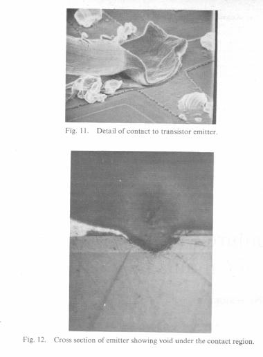
An example of this failure mode is depicted in an n-p-n transistor which was greatly overstressed. Fig. 11 shows an enlarged view of the emitter wire bond which appears de- pressed into the silicon. A cross sectional photomicrograph of this bond area (Fig. 12) reveals the formation of a very deep pit into the silicon. The pit extends through the collec- tor-base junction and nearly reaches the epitaxial layer junction. Formation of this void, which developed in the silicon under the wire bond at the high current density re- gion, was due to mass transfer by silicon dissolution into
the aluminum and transport down the aluminum conductor by interaction with the electronic wind.
V. CONCLUSIONS Two failure modes for silicon devices and integrated cir-
cuits utilizing aluminum metalization have been described. These are both caused by electromigration. Equations en- abling prediction of the lifetime of aluminum conductors containing no gradients in current density, temperature, or ion diffusion coefficient have been presented. For typical small conductor geometries failures due to this process be- come important (lifetime less than 10 years) at current den- sities exceeding 5 x lo4 A,’cmZ and temperatures in excess of 150°C. It has also been shown qualitatively that a positive gradient (in terms of electron flow direction) of metal ion diffusivity in the conductor will establish a region where vacancies preferentially condense. Similar effects should be caused by positive gradients in current density or tempera- ture.
The formation of etch pits into silicon has been shown qualitatively to occur under the influence of elevated tem- perature and high current density at aluminum-silicon con- tacts, where the electrons flow out of the silicon and into the aluminum or where the major component of electron flow is parallel to the aluminum-silicon interface. Device failure can occur when an etch pit (filled by aluminum) grows across an underlying junction resulting in a short.
ACKNOWLEDGMENT The scanning electron microscope pictures were made by
John Devaney of the Jet Propulsion Laboratory, Pasadena, Calif.
REFERENCES [l] K. E. Schwartz, Elektro!vrische Wanderuny in Jiissiyen undfesten
[2] W. Seith, Dzfision in Metallen. Berlin: Springer-Verlag, 1955. [3] V. B. Fiks, “On the mechanism of the mobility of ions in metals,”
Socier Phys.-Solid-State, vol. 1, p. 14, no. 1, 1959. [4] H. B. Huntington and A. R. Grone, “Current-induced marker
motion in gold wires,” J . Phys. Chem. Solids, vol. 20, pp. 7687, nos. 1/2, 1961.
[SI A. R. Grone, “Current induced marker motion in copper,” J . Phys. Chem. Solids, vol. 20, pp. 88-98, nos. 112, 1961.
[6] R. V. Penney, “Current-induced mass transport in aluminum,’’ J. Phys. Chem. Solids, vol. 25, pp. 335-345, 1964.
[7] J. F. D’Amico and H. B. Huntington, “Electromigration and
Polytechnic Institute (RPI), Troy, N. Y., Rept. 1044-19. thermomigration in gamma-uranium,” Dept. of Phys., Rensselaer
[8] G. A. Sullivan, “Search for a reversal in copper electromigration,” RPI Dept. of Phys. Rept. 1044-8.
[9] P. S. Ho, “Electromigration and soret effect in cobalt,” J . Phys. Chem. Solids, vol. 27, pp. 1331-1338,1966.
[lo] P. D. Ho and H. B. Huntington, “Electromigration and void ob- servation in silver,” J . Phys. Chem. Solids, vol. 27, pp. 1319-1329, 1966.
[ l l ] A. Ladding, “Current induced motion of lattice defects in indium metal,” J. Phys. Chem. Soli&, vol. 26, pp. 143-151, 1965.
[12] I. A. Blech, and H. Sello, et al., RADC Tech. Rept. TR 66-31, December 1965.
[13] I. A. Blech and H. Sello, 5th Annual Symposium on Physics of Failure in Electronics, Columbus, Ohio, November 1966.
[14] W. Mutter, The Electrochemical Society, Spring Meeting, Dallas, Abstract 62, p. 96, May 1967.
[15] D. Chhabra and N. Ainsley, IBM Components Division, E. Fishkill Facility, N. Y., Tech. Rept. 22.419, July 1967.
[16] J. R. Black, “Mass transport of aluminum by momentum exchange
Metallen. Leipzig, 1940.
Authorized licensed use limited to: PORTLAND STATE UNIVERSITY. Downloaded on March 29, 2009 at 03:40 from IEEE Xplore. Restrictions apply.

1594 PROCEEDINGS OF THE IEEE, VOL. 57, NO. 9, SEPTEMBER 1969
with conducting electrons,” Proc. 1967 Annual Syrnp. Reliability Physics, IEEE Cat. 7-15C58, November 1967.
[17] P. B. Ghate, Appl. Phys. Letters, vol. 11, p. 14, 1967. [18] J. R. Black, “Metalization failures in integrated circuits,” RADC
Tech. Rept., TR-68-243, October 1968. [19] ---, “Aluminum conductor failure by mass transport,” h o c . 3rd
Internatl. Congr. Microelectronics, Munich, November 1968. [20] -, “Electromigration-A brief survey and some recent results,”
IEEE Trans. Electron Devices, vol. ED-16, pp. 338-347, April 1969. [21] T. E. Hartman and J. C. Blair, “Electromigration in thin gold films
conductor,” IEEE Trans. Electron Devices, vol. ED-16, pp. 407-410, April 1969.
[22] M. J. Attardo, A. H. Landzberg, W. E. Reese, and G. T. Wenning, “Aluminum electromigration in long stripes,” presented at the 7th
Annual Reliability Physics Symp., Washington, D. C., December 211, 1968.
[23] J. Spokas and C. P. Slichter, “Nuclear relaxation in aluminum,” Phys. Rev., vol 113, pp. 1462-1472, March 15, 1959.
[24] J. Bass, “The formation and motion energies of vacancies in alumi- num,’’ Phil Mag., vol. 15, pp. 717, April 1967.
[25] The etch formula for stripping of aluminum consisted of 2 parts by volume of distilled water, 1 part nitric acid, 1 part acetic acid, and 16 parts phosphoric acid.
[26] M. Hansen, Constitution ofBinary Alloys. New York: McGraw-Hill, 1958.
[27] From data presented by G. Schnable, R. Keen, and L. Lowenstern, “Study of contract failures in integrated circuits,” Tech. Rept. RADC-TR-67-331, September 1967.
Void Formation Failure Mechanisms in Integrated Circuits
BERNARD SELIKSON, SENIOR MEMBER, IEEE
Abstract-The several interfacial regions where voids and electri- cal opens occur in semiconductor discrete devices and monolithic integrated circuits are described. The metals used at these interfaces in circuits today are listed and a description is given of the void- producing mechanisms applicable to each area, along with techniques for their detection. Voids which develop in the bond of gold wire, which is ball bonded to aluminum metalization as a result of inter- metallic purple plague formation, are explained as an example of the Kirkendall effect. However, the faster diffusion of one of the metals of a bond producing voids cannot explain the observation of voids in both the gold and the aluminum side of the bond. Recent thin film experiments account for this effect by a process which is rate limited by diffusion through the newly formed intermetallic phase. Analysis of five newer alternate metalization systems for circuits show them all to have the potential for compound formation, which may be ex- pected to be accompanied by void formation.
INTRODUCTION HE OCCURRENCE of voids in semiconductor dis- crete devices and monolithic integrated circuits has been observed and studied for some time [l 1. Gen-
erally, these voids are a source of poor device performance and lead ultimately to device failure. In the present paper the various void regions in integrated circuits are identified and their origins are described. Voids which result from compound formation are discussed in some detail and re- cent work is described which helps to elucidate the kinetics of the failure mechanism. In addition, the various metaliza-
Manuscript received January 21, 1969; revised February 6, 1969. The author is with Lowell Technological Institute, Lowell, Mass.
and General Electric Company, Integrated Circuits Project, Syracuse, N. Y.
tion-bond interconnect systems in use today are described and analyzed as to their void-forming potential.
DISCUSSION Voids and electrical opens occur at a number of distinct
regions in monolithic integrated circuits. As indicated in Fig. 1, voids or opens have been observed 1) at the semi- conductor-header bond, 2) at the semiconductor-metal contact, 3) at the metalization-oxide interface, 4) along the metalization overlay metal, 5 ) at the metalization-wire bond on the semiconductor, and 6 ) at the wire-post bond out at the header or flat pack frame.
The typical metals used at these interfaces are given below and discussed later from a systems reliability point of view.
1) The low silicon-gold eutectic temperature of 370°C dictates gold as the most common metal used for soldering silicon to the header or flat pack.
2) Aluminum is the most widely used ohmic contact metal to silicon. Other contact metals more recently used are chromium, titanium, molybdenum, silver, or platinum.
3) Overlay metals used are aluminum, gold, molybde- num, silver, silver-gold alloy, or titanium.
4) Gold or aluminum wire are most commonly used to connect the integrated circuit from the semiconductor to the posts at the package frame.
5 ) The posts are usually gold plated Kovar, but for high reliability circuits, aluminum clad Kovar may be used.
Void formation and electrical opens occur in integrated circuits either because of some faulty processing during the
Authorized licensed use limited to: PORTLAND STATE UNIVERSITY. Downloaded on March 29, 2009 at 03:40 from IEEE Xplore. Restrictions apply.

Authorized licensed use limited to: PORTLAND STATE UNIVERSITY. Downloaded on March 29, 2009 at 03:40 from IEEE Xplore. Restrictions apply.

Authorized licensed use limited to: PORTLAND STATE UNIVERSITY. Downloaded on March 29, 2009 at 03:40 from IEEE Xplore. Restrictions apply.

Authorized licensed use limited to: PORTLAND STATE UNIVERSITY. Downloaded on March 29, 2009 at 03:40 from IEEE Xplore. Restrictions apply.
Authorized licensed use limited to: PORTLAND STATE UNIVERSITY. Downloaded on March 29, 2009 at 03:40 from IEEE Xplore. Restrictions apply.

Authorized licensed use limited to: PORTLAND STATE UNIVERSITY. Downloaded on March 29, 2009 at 03:40 from IEEE Xplore. Restrictions apply.
Authorized licensed use limited to: PORTLAND STATE UNIVERSITY. Downloaded on March 29, 2009 at 03:40 from IEEE Xplore. Restrictions apply.