Embed Size (px)
Citation preview

Mesoporous SnO2 Single Crystals as an Effective
Electron Collector for Perovskite Solar CellsZonglong Zhu†‡1, Xiaoli Zheng‡1, Yang Bai†, Teng Zhang†‡, Zilong Wang‡,
Shuang Xiao†‡, Shihe Yang†‡*
†Nano Science and Technology Program, ‡Department of Chemistry, ⊥The Hong
Kong University of Science and Technology, Clear Water Bay, Kowloon, Hong Kong
Electronic Supplementary Material (ESI) for Physical Chemistry Chemical Physics.This journal is © the Owner Societies 2015
Experimental section
Preparation of SiO2 colloid. Colloid silica nanospheres (diameter: ∼50 nm) were
synthesized by mixing 10.6 mL of H2O (18.2 MΩ, Millipore Milli-Q), 6 mL of
ammonium hydroxide (28%, VWR International S.A.S.), and 250 mL of ethanol
(≥99.9%, Merck) in a 500 mL three-neck flask at room temperature. Next, 33 mL of
tetraethyl orthosilicate (98%, Aldrich) was added in the flask quickly, and the mixture
was stirred at 700 rpm for 24 h at room temperature. Then the product was
centrifuged at 7000 rpm for 1 h, and the translucent solid was collected and sintered at
500°C for 30 min (ramping time 150 min).
Preparation of SnO2 mesoporous single crystals. 1.4 g of SnCl4.5H2O was added to
28 ml of ethanol/water (v/v = 1/1) mixed solvent. After the mixture was stirred for 10
min, 1.4 ml of HCl (37 wt%) was added and stirred for another 10 min. Then 0.8 g of
SiO2 was added in the autoclave and the sealed vessel was heated at 200°C for 12 h in
an oven. Afterward, the vessel was cooled to room temperature naturally, and the
solid particles settled at the bottom were collected. Then the solid particles were
washed with a large amount of water by vacuum filtration. Finally, the silica template
was removed by etching in 2 M NaOH at 80°C for 1 h. Then the remaining SnO2
products were collected by centrifugation and washed with H2O and ethanol several
times. The SnO2 MSC paste were deposited from suspension in the ethanol and
terpineol (v/v 1:2) with the concentration 5 wt%.
Solar cell fabrication. The material synthesis and solar cell fabrication were
according to a reported procedure by Michael Gratzel et al.1 Before depositing
CH3NH3PbI3, the SnO2 MSC paste was spin-coated onto patterned fluorine doped tin
oxdie (F:SnO2) coated glass (FTO). Then, the film was annealing at 300 °C for 30 min.
For the TiO2 coated SnO2 MSC film, the SnO2 films were immersed in 50 mM of
TiCl4 aqueous solution at 70 °C for 0.5 h and heat-treated at 500 °C for 30 min. The
TiO2 nanocyrstals (with 50 nm size diameters) paste were also spin-coated onto the
FTO by 3000 rpm and annealing at 500 °C for 1 h, the films were also treated in TiCl4
solution by the method above.
PbI2 (450 mg/ml) in N,N-dimethylformamide (DMF) was spin-coated onto the
above films, and then was dipped in a solution of CH3NH3I in 2-propanol (10 mg/ml)
for 20 s and rinsed with 2-propanol. The hole transport layer was used by spin-coating
a solution of spiro-MeOTAD, which contains chlorobenzene (130 mg/ml), 26 ul of
tert-butylpyridin (TBP) solution and 35 ul of Li-bis(trifluoromethanesulfonyl) imide
(Li-TFSI)/acetonitrile (170 mg/ml). For the metal electrode, 50 nm thickness of gold
was deposited on the top of the HTM by a thermal evaporation through a metal
shadow mask to define the active area of the devices (~7 mm2) and to form a top
anode. The cell was packaged by scribbling UV-glue on the top and covered a glass
slides, then the cell was exposed to UV light radiation for 10 min to make the glue
solidify. The device testing was carried out the glove box after packaging and tested
within a metal mask of an aperture (7 mm2 area).
Characterization. Morphologies of the nanomaterials and subsequent nanostructures
were directly examined on JEOL6700F SEM at an accelerating voltage of 5 kV. More
detailed structural examinations were carried out by transmission electron microscopy
(TEM, JEOL 2010F) and high resolution TEM with an accelerating voltage of 200 kV.
Powder X-ray diffraction (XRD) patterns were recorded on a Philips high-resolution
X-ray diffraction system (model PW1830) with Cu Kα radiation (λ=1.5406 Å). The
light source (Oriel solar simulator, 450 W Xe lamp, AM 1.5 global filter) was
calibrated to 1 sun (100 mW cm–2) using an optical power meter (Newport, model
1916-C) equipped with a Newport 818P thermopile detector. J–V characteristic
curves and intensity modulated photocurrent/photovoltage spectroscopy (IMPS/IMVS)
were measured by the Zahner controlled intensity modulated photoresponse
spectroscopy (C-IMPS) system. We measured the EIS spectra at open voltage and a
frequency range from 1Hz and 1MHz with AC amplitude of 10 mA under
illumination of simulated solar AM1.5 global light at 100mWcm-2. Z-View Analyst
software was used to model the Nyquist plots obtained from the impedance
measurements. Incident photon to current conversion efficiencies (IPCEs) was
measured on photo current spectra system of CIMPS (CIMPS-PCS) with tunable light
source (TLS03).

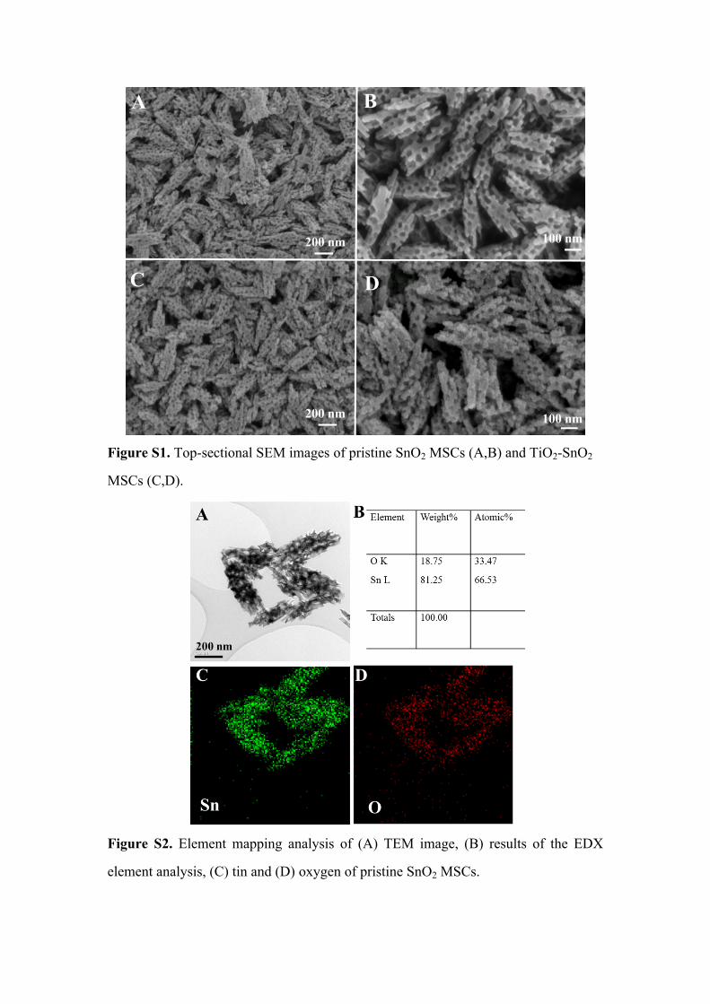
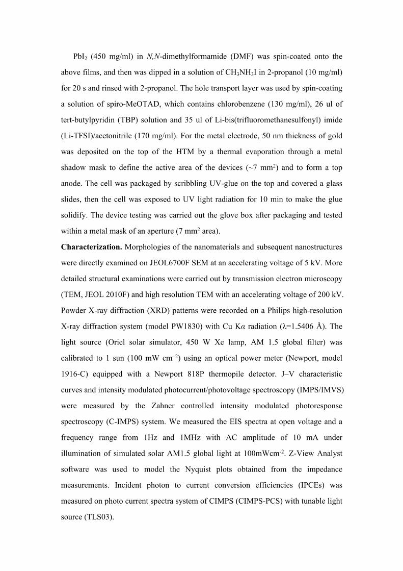
Figure S1. Top-sectional SEM images of pristine SnO2 MSCs (A,B) and TiO2-SnO2
MSCs (C,D).
Figure S2. Element mapping analysis of (A) TEM image, (B) results of the EDX
element analysis, (C) tin and (D) oxygen of pristine SnO2 MSCs.
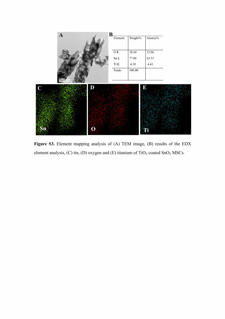
Figure S3. Element mapping analysis of (A) TEM image, (B) results of the EDX
element analysis, (C) tin, (D) oxygen and (E) titanium of TiO2 coated SnO2 MSCs.
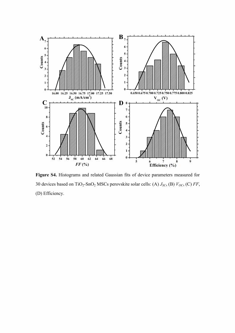
Figure S4. Histograms and related Gaussian fits of device parameters measured for
30 devices based on TiO2-SnO2 MSCs perovskite solar cells: (A) JSC, (B) VOC, (C) FF,
(D) Efficiency.
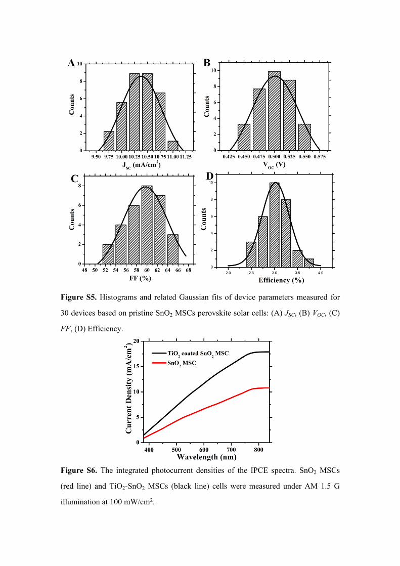
Figure S5. Histograms and related Gaussian fits of device parameters measured for
30 devices based on pristine SnO2 MSCs perovskite solar cells: (A) JSC, (B) VOC, (C)
FF, (D) Efficiency.
Figure S6. The integrated photocurrent densities of the IPCE spectra. SnO2 MSCs
(red line) and TiO2-SnO2 MSCs (black line) cells were measured under AM 1.5 G
illumination at 100 mW/cm2.
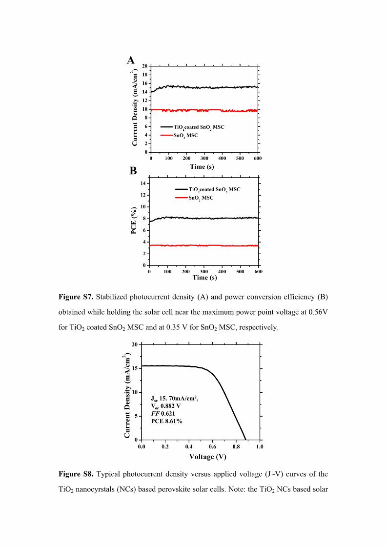
Figure S7. Stabilized photocurrent density (A) and power conversion efficiency (B)
obtained while holding the solar cell near the maximum power point voltage at 0.56V
for TiO2 coated SnO2 MSC and at 0.35 V for SnO2 MSC, respectively.
Figure S8. Typical photocurrent density versus applied voltage (J~V) curves of the
TiO2 nanocyrstals (NCs) based perovskite solar cells. Note: the TiO2 NCs based solar
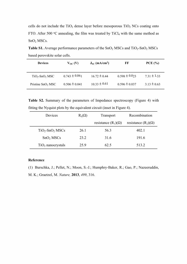
cells do not include the TiO2 dense layer before mesoporous TiO2 NCs coating onto
FTO. After 500 oC annealing, the film was treated by TiCl4 with the same method as
SnO2 MSCs.
Table S1. Average performance parameters of the SnO2 MSCs and TiO2-SnO2 MSCs
based perovskite solar cells.
Devices VOC (V) JSC (mA/cm2) FF PCE (%)
TiO2-SnO2 MSC 0.743 1± 0.06 16.72 0.44± 0.598 23± 0.0 7.31 33± 1.
Pristine SnO2 MSC 0.506 0.041± 10.33± 0.61 0.596 0.037± 3.13 0.63±
Table S2. Summary of the parameters of Impedance spectroscopy (Figure 4) with
fitting the Nyquist plots by the equivalent circuit (inset in Figure 4).
Devices Rs(Ω) Transport
resistance (R1)(Ω)
Recombination
resistance (R2)(Ω)
TiO2-SnO2 MSCs 26.1 56.3 402.1
SnO2 MSCs 23.2 31.6 191.6
TiO2 nanocrystals 25.9 62.5 513.2
Reference
(1) Burschka, J.; Pellet, N.; Moon, S.-J.; Humphry-Baker, R.; Gao, P.; Nazeeruddin,
M. K.; Graetzel, M. Nature, 2013, 499, 316.


![((Title)) · Web viewtandem dye sensitised solar cells and as hole collector in BHJ solar cells.[16] More recently NiO has also found application in perovskite heterojunction solar](https://img.pdfslide.net/doc/110x75/5e3d4e3986087531790bf435/title-web-view-tandem-dye-sensitised-solar-cells-and-as-hole-collector-in-bhj.jpg)