Embed Size (px)
Citation preview

ELECTRON EMISSION THERMAL ENERGY CONVERSION
A Thesis presented to the
Graduate School Faculty
UNIVERSITY OF MISSOURI – COLUMBIA
In Partial Fulfillment of the
Requirements for a Master of
Science - Mechanical Engineering
By
DOMINICK LOVICOTT
Dr. Gary Solbrekken Thesis Supervisor
JULY 2010

The undersigned, appointed by the dean of the Graduate School, have examined the
thesis entitled
ELECTRON EMISSION THERMAL ENERGY CONVERSION
presented by Dominick Lovicott,
a candidate for the degree of Master of Science of Mechanical Engineering
and hereby certify that, in their opinion, it is worthy of acceptance.
Assistant Professor Gary Solbrekken
Professor Frank Feng
Assistant Professor Gregory Triplett

ii
ACKNOWLEDGEMENTS
I would like to acknowledge the extreme patience that Dr. Solbrekken has
shown over the course of writing this thesis. His dedication to this project and
my education has been pivotal to the success of this work and his guidance and
mentoring has unquestionably made me a better engineer.
I would like to acknowledge Jeff Scott and Dr. Li for their significant
contribution to this work. Jeff Scott and Dr. Li have made the first step toward
fabrication of TFE nanowire convertor by growing Si nanowires. Their
contribution has formed the foundation for prototyping the device explored in
this work. All pictures and nanowire fabrication processes described in chapter 6
were performed by Jeff Scott and Dr. Hao Li.

iii
ELECTRON EMISSION THERMAL ENERGY CONVERSION
Dominick A. Lovicott
Dr. Gary Solbrekken Thesis Supervisor
ABSTRACT
Energy consumption is driving both an intellectual and financial investment into
the exploration of alternative energy sources and more efficient use of that energy.
Efficient energy conversion for electrical power generation is a key component of
curbing the world’s ever increasing energy demands and waste heat is one of the
primary byproducts of inefficient energy consumption. In general, high temperature
heat sources are easier to be efficiently harvested and low temperature or low grade
waste heat is more challenging to recover because of the small temperature delta.
Appreciable adoption of low grade waste heat recovery will require devices that can
convert low temperature waste heat efficiently into useful electrical power.
Electron emission from a surface can be achieved via two mechanisms:
tunneling and thermionics. Converting thermal energy to electrical power using these
mechanisms is achieved by generation of an electron current from the emitter to the
collector, and production of a voltage potential between electrodes due to the potential
energy difference between the electrodes. Efficient low temperature energy conversion
is investigated in this thesis utilizing these two emission mechanisms.

iv
Two device concepts were developed based on thermal field (a form of
tunneling) and thermionic emission that incorporate nontraditional design elements and
novel implementations of existing technologies. These device concepts were developed
with the intent to help mitigate some of the common downfalls of this solid state energy
conversion.
In addition to the novel implementation and device concepts, a unique system
level modeling approach is taken that combines a more detailed thermal network with
the emission modeling. Advantages of this method include a better estimate for
boundary conditions and emission temperatures. Typically emission models assume
constant temperature boundary conditions which can over estimate device
performance.
Modeling of a magnetically enhanced thermionic diode illustrated significant
reductions in thermal radiation exchange between emitter and collector. This reduction
is attributed to the ability to spatially reorient the electrodes due to the magnetically
altered electron trajectories, and was shown to have a substantial effect on the energy
conversion efficiency. Efficient low temperature thermionic energy conversion is
currently not viable due to the high temperatures required to excite electrons above the
material work function. With lower material work functions, low temperature
thermionic energy conversion would be achievable.
The second design concept investigated in this thesis utilizes the transition
region between field emission and thermionic emission known as thermal-field

v
emission. This type of emission uses a high electric field produced by a gate electrode to
increase the probability of electron tunneling. High electric fields at relatively low gate
voltages are achieved by concentrating the field around nanowire tip emission sites.
Unlike field emission, the electrode is heated by a heat source which further increases
the probability of electron emission. Unlike thermionic devices, which suffer poor
emission rates at low temperature, the thermal-field nanowire converter can produce
appreciable emission at low temperatures. Modeling showed promising conversion
efficiencies for this device at low temperature. However, the model does not account
for gate leakage currents which will likely be the primary obstacle of this technology.
Initial steps towards fabrication of this device have been taken including the growth of
Si nanowires.
vi
TABLE OF CONTENTS
ACKNOWLEDGEMENTS ................................................................................................. II
ABSTRACT. .............................................................................................................. III
LIST OF TABLES ....................................................................................................... VIII
LIST OF FIGURES ...................................................................................................... VIII
NOMENCLATURE ...................................................................................................... XV
1. INTRODUCTION .................................................................................................. 1
2. BACKGROUND .................................................................................................... 7
i. Direct Power Generation .................................................................................. 7
a. Battery Replacement ............................................................................................... 8
b. Pulse Power Source .................................................................................................. 9
ii. Indirect Power Generation ............................................................................. 11
a. Automotive Waste Heat ........................................................................................ 13
b. Server Component Waste Heat ............................................................................. 14
iii. Reference Concept ......................................................................................... 18
3. EMISSION PHYSICS ............................................................................................ 21
i. Fermi Level, Work Function & The Potential Barrier ..................................... 23
ii. Thermionic Emission ....................................................................................... 29
iii. Tunneling ........................................................................................................ 36
a. Field Emission ......................................................................................................... 39
b. Thermal-Field Emission .......................................................................................... 45
iv. Emission Comparison ..................................................................................... 51
v. Space Charge .................................................................................................. 54

vii
a. Derivation of Child-Langmuir Equation .................................................................. 55
b. Methods for Controlling Space Charge .................................................................. 63
4. INTEGRATION OF EMISSION BASED DEVICE INTO A SYSTEM ............................................ 67
i. Thermodynamic Background.......................................................................... 67
ii. Magnetic Diode .............................................................................................. 69
a. System Description ................................................................................................ 69
b. Thermal Radiation View Factor .............................................................................. 70
c. Enclosure Modeling ............................................................................................... 72
d. Thermal Radiation Recovery Method .................................................................... 76
iii. TFE Nanowire Convertor ................................................................................ 79
a. System Description ................................................................................................ 79
b. Thermal Modeling .................................................................................................. 80
c. Thermal Resistance Network ................................................................................. 81
d. Energy Balance ....................................................................................................... 85
5. ANALYSIS OF SYSTEM ......................................................................................... 89
i. Iterative Solving .............................................................................................. 89
ii. Magnetic Diode Convertor ............................................................................. 90
a. Magnetic Field ........................................................................................................ 90
b. Space Charge .......................................................................................................... 96
c. 1st Order Analysis ................................................................................................... 97
d. 2nd Order Analysis ................................................................................................ 100
e. Radiation Recovery Analysis ................................................................................ 105
iii. TFE Nanowire Convertor .............................................................................. 110
a. Electric Field ......................................................................................................... 112
b. Tip Emission & Field Emitter Arrays ..................................................................... 113
c. Server Waste Heat Application ............................................................................ 117
6. PROPOSED FABRICATION OF NANOWIRE BASED STRUCTURE ....................................... 122

viii
7. CONCLUSIONS AND FUTURE STUDIES ..................................................................... 128
i. Magnetic Diode ............................................................................................ 129
ii. TFE Nanowire Convertor .............................................................................. 130
8. APPENDIX….. ................................................................................................. 132
i. Generic Thermionic Model ........................................................................... 132
ii. Magnetic Diode Model ................................................................................. 134
REFERENCES .......................................................................................................... 137
LIST OF TABLES
Table 2.1 Identified server component specifications .........................................................18
Table 3.1 Tabulated values of work functions for various materials .............................28
Table 3.2 Space charge model summary ....................................................................................66
Table 5.1 Approximate magnetic field sources (Serway and Beichner 2000) ............93
Table 5.2 Tabulated empirical results for arrays of field emitters with nanoscale tip emitters (Nation, et al., 1999)(Pan, et al., 2000)(Teo, et al., 2002) ........... 117
LIST OF FIGURES
Fig. 1.1 US energy consumption and US energy production (Energy Information Administration 2006) ...................................................................................................... 1
Fig. 1.2 US energy expenditures (Energy Information Administration 2006) .......... 2
Fig. 1.3 World marketed energy consumption by region (Energy Information Administration 2007) ...................................................................................................... 2
Fig. 1.4 World Electricity generation by fuel source (Energy Information Administration 2007) ...................................................................................................... 3
ix
Fig. 1.5 Source of carbon dioxide emission by industry and fuel source ................... 4
Fig. 2.1 Plot of Analytic and Numeric approximations of the transient thermal response of an energetic material reaction...........................................................10
Fig. 2.2 Motor vehicle trending for fuel rate (miles per gallon) (Energy Information Administration 2006) ..........................................................................13
Fig. 2.3 Historical and projected datacenter energy consumption trends (EPA 2007) ....................................................................................................................................15
Fig. 2.4 Reference concept – baseline configuration ........................................................20
Fig. 3.1 Illustration of thermionic (A) and tunneling (B) emission mechanisms ..23
Fig. 3.2 Thermionic potential barrier adopted from (Angrist 1976) .........................24
Fig. 3.3 Fermi-Dirac Distribution for a material with a Fermi level of 2 eV ............26
Fig. 3.4 Illustration of the relationship between ionization energy, work function and the Fermi level as described in Equation 3.3 ...............................................27
Fig. 3.5 Plot of work function temperature variation for Tungsten, and estimates for TI current densities using a fixed (T=0K) and temperature dependant work functions..................................................................................................................29
Fig. 3.6 Plots of flat plate thermionic emission currents for (A) work functions ranging from 2 eV to 5 eV to illustrate high temperature emission, and (B) work functions ranging from 2.0 eV to 2.3 eV to illustrate low temperature emission ...................................................................................................35
Fig. 3.7 Theoretical thin potential barrier ............................................................................37
Fig. 3.8 Flat plate potential barrier example .......................................................................38
Fig. 3.9 Plot of flat plate (β=1) cold cathode field emission current densities for work functions ranging from 2.1 eV to 2.3 eV ......................................................41
Fig. 3.10 Illustration of a (a) spherical tip emitter and gate electrodes and (b) electric field model using concentric spheres (Brodie & Schwoebel, 1994).. ..................................................................................................................................42
Fig. 3.11 Illustration of the prolate-spheroidal coordinate system used to derive the geometric enhancement factor in equation 3.37 (Zuber, Jensen, & Sullivan, 2002) ..................................................................................................................43

x
Fig. 3.12 Electron Transport Mechanisms: (a) Thermionic (TI), Thermal-Field (TFE), and Field (FE) Emission, (b) Approximate Energy Distributions for Emitted Electrons ............................................................................................................45
Fig. 3.13 Plot of approximated ω values based on equation 3.45 at constant temperature 400 K..........................................................................................................48
Fig. 3.14 Plot of thermal field emission current densities for various work functions (2.0 – 2.3 eV) with respect to applied electric field .......................49
Fig. 3.15 Plot of thermal field emission current densities for various work functions (2.0 – 2.3 eV) with respect to temperature .......................................50
Fig. 3.16 Plot of potential energy barrier (“SURFACE POTENTIAL BARRIER”) that includes the FE region (Region I), the TFE region (Region II) and the TI region (Region III). (Dolan & Dyke, 1954) .............................................................52
Fig. 3.17 Plots of the energy distributions for emitted electrons at various temperatures and applied electric fields (Dolan & Dyke, 1954) ..................53
Fig. 3.18 Plot of the three emission regions as a function of temperature and electric field (Murphy & Good Jr., 1956) ................................................................54
Fig. 3.19 Metal lattice (a) prior to emission with no space charge, and (b) after emission with space charge caused by emitted electrons ...............................55
Fig. 3.20 Langmuir’s findings for current at various emitter temperatures and collector voltages with a gap of 1.2 cm (Langmuir 1913) ...............................56
Fig. 3.21 Case for derivation of Child-Langmuir space charge model ...........................57
Fig. 3.22 Plot illustrating the voltage required for the initial velocity to equal the potential voltage induced velocity at a given temperature, and the voltage required for the initial velocity to be one order of magnitude less (negligible) than the potential voltage induced velocity for a given temperature.......................................................................................................................60
Fig. 3.23 Comparison of the Child-Langmuir model with the Richardson model ....62
Fig. 3.24 Comparison of the Langmuir model (including initial velocities) with the Richardson model ...........................................................................................................63
Fig. 3.25 Space charge control utilizing narrow gap dimensional constraint ............64
Fig. 3.26 Space charge control utilizing positive ions .........................................................65
xi
Fig. 3.27 Space charge control using a gate electrode .........................................................65
Fig. 4.1 Thermal heat engine operating between two thermal reservoirs ..............68
Fig. 4.2 Simplified magnetic diode ..........................................................................................70
Fig. 4.3 Illustration of parallel, perpendicular and 180° plate orientations ...........71
Fig. 4.4 Thermal radiation view factor for angles between emitter and collector varying from 0 to 180 degrees ...................................................................................72
Fig. 4.5 Radiosity resistance network of a Magnetic converter within an enclosure. ...........................................................................................................................73
Fig. 4.6 Simplified radiosity network .....................................................................................74
Fig. 4.7 Non-insulated enclosure radiosity network ........................................................75
Fig. 4.8 Thermal radiation recovery orientation ...............................................................76
Fig. 4.9 Method for determining the view factor between the emitter and collector plates for the thermal radiation recovery orientation ...................77
Fig. 4.10 Thermal radiation view factor for plates of unequal dimension separated by some distance L ..........................................................................................................77
Fig. 4.11 Thermal radiation view factor for varying plate separation distances ......78
Fig. 4.12 Simplified TFE nanowire convertor .........................................................................79
Fig. 4.13 Detailed TFE convertor thermal resistance network ........................................82
Fig. 4.14 Simplified TFE convertor thermal resistance network ....................................84
Fig. 4.15 Device level energy balance ........................................................................................86
Fig. 4.16 Detailed collector side energy balance. ..................................................................86
Fig. 4.17 Detailed emitter side energy balance ......................................................................87
Fig. 4.18 Simplified collector side energy balance ................................................................87
Fig. 4.19 Simplified emitter side energy balance ..................................................................88
Fig. 5.1 Flow chart illustrating iterative method used to solve electromechanical models .................................................................................................................................90
xii
Fig. 5.2 Illustration of electron trajectory due to B-field ................................................91
Fig. 5.3 Magnetic field, B required for an electron radius, r emitted from a surface at 500K, 1000K, and 1500K.........................................................................................92
Fig. 5.4 Collector orientations considered with the presence of a magnetic field .93
Fig. 5.5 Magnetic triode as adopted from (Hatsopoulos and Gyftopoulos 1973) ..94
Fig. 5.6 Magnetic triode efficiency (Hatsopoulos and Gyftopoulos 1973) ................95
Fig. 5.7 Illustration of space charge limitation for an emitter at 1000 K with a work function of 2 eV .....................................................................................................97
Fig. 5.8 Magnetic converter first order analysis with constant temperature electrodes ...........................................................................................................................98
Fig. 5.9 Efficiency of magnetic triode for varying emitter temperatures and angles. The collector plate is assumed to operate at 400 K and the work functions for the emitter and collector being 3 eV and 1 eV respectively. The enclosure is assumed to be a constant 0 K. ..................................................99
Fig. 5.10 Illustration of magnetic converter with non constant temperature boundaries and an insulated enclosure ............................................................... 101
Fig. 5.11 Emitter energy balance assuming no temperature distribution within emitter material ............................................................................................................ 102
Fig. 5.12 Collector energy balance assuming no temperature distribution within collector material ......................................................................................................... 102
Fig. 5.13 Magnetic device concept minimizing thermal radiation losses ................. 105
Fig. 5.14 Unit cell boundary used to analyze device concept ........................................ 106
Fig. 5.15 Device efficiency for varying plate separation. The emitter and collector temperatures are 1000 K and 300 K, respectively. The emitter and collector work functions are 2 eV and 1 eV, respectively. ............................ 107
Fig. 5.16 Device efficiency and power density for varying emitter temperatures. The emitter and collector work functions are 2 eV and 1 eV, respectively…. ................................................................................................................ 108
Fig. 5.17 Device efficiency and power density for varying emitter work functions. The collector work function is assumed to be 1 eV. The emitter and

xiii
collector source temperatures are assumed to be 1000 K and 300 K, respectively..................................................................................................................... 109
Fig. 5.18 An illustration of the proposed TFE nanowire convertor ............................ 111
Fig. 5.19 Electric field strength for various tip radii and operating voltages.......... 113
Fig. 5.20 Thermal-Field Emission using 3C SiC (Work Function ~ 4.4 eV) based on the projected emitter area ........................................................................................ 114
Fig. 5.21 Illustration gated field emitter array (Nation, et al. 1999) .......................... 115
Fig. 5.22 SEM of gated field emitter array (Nation, et al. 1999) ................................... 115
Fig. 5.23 Illustration of the experimental setup used to evaluate SiC nanowire field emission (Z. Pan, et al. n.d.) ...................................................................................... 116
Fig. 5.24 Proposed server implementation the TFE convertor .................................... 118
Fig. 5.25 TFE generated power density for a range of applied gate voltages (11.5V -13.0 V) and component temperatures with a 10nm tip radius, 3 eV emitter work function, 1.6 eV collector work function, and ambient temperature of 300 K.................................................................................................. 119
Fig. 5.26 TFE generated power density from a 150 W device for a range on nanowire radii (5 nm – 15 nm) and applied gate voltages with a 400 K component temperature, 300 K ambient temperature, 3 eV emitter work function, and 1.6 eV collector work function ..................................................... 120
Fig. 5.27 Plot of (a) power density, current density, operating voltage, and (b) efficiencies as function of load resistance .......................................................... 121
Fig. 6.1 Sketch of the theoretical Si nanowire that results from SiO vapor and VLS mechanism. Adapted from (Kolb, et al. 2004) by (Scott and Solbrekken n.d.) .................................................................................................................................... 123
Fig. 6.2 SEM images of a single layer of polystyrene spheres (Scott and Solbrekken n.d.) ............................................................................................................ 124
Fig. 6.3 SEM images of patterned gold film resulting from a single layer of polystyrene spheres (Scott and Solbrekken n.d.) ............................................ 124
Fig. 6.4 SEM images of Si nanowire growth (gray lines), as well as a large number of SiO2 deposits (white dots) (Scott and Solbrekken n.d.) ........................... 125

xiv
Fig. 6.5 Free standing SiC nanowires made from graphite particles and carbon nanotubes (Photos courtesy of Dr. Hao Li) ........................................................ 126
Fig. 6.6 Proposed experiment for TFE convertor prototype ...................................... 126

xv
NOMENCLATURE
Half the foci distance (m)
Cross sectional area (m^2)
Thermionic emission constant (A/cm2K2)
Magnetic field (T)
Specific heat of solid or liquid (kJ/mol K)
Specific heat of vaporization at constant temperature (kJ/mol K)
Constant of integration
Universal constant
Electrode gap (m)
Tunneling transmission coefficient
Charge of an electron (Coulomb)
Energy (eV)
TFE variable in chapter 3.iii.b
Permittivity of free space (F/m)
Fermi distribution
Electric field in chapter 3 (V/m)
Thermal radiation view factor in chapters 4 and 5
Force due to a magnetic field (N)
Plank constant (eV s)
Reduced Plank constant (eV s)
Molar heat of vaporization of a monatomic gas (kJ/mol)
Latent heat of vaporization at constant temperature (kJ/mol)
xvi
Current density (A/cm2)
TFE variable
Boltzmann’s constant (m2 kg/s2 K)
TFE variable
Plate gap (m)
Mass (kg)
Molecular weight
Number per unit volume in chapter 3 section i
Number per unit area in chapter 3 section ii
Summation index variable in chapter 3.iii
Electron supply function (1/cm2 s eV)
Avogadro ’s number (mol-1)
Pressure (Pa)
Particle charge (Coulomb)
Heat/thermal energy (W)
Emitter tip radius in chapter 3 (m)
Electron trajectory radius of curvature in chapter 5 (m)
Gate electrode radius (m)
Universal gas constant (kJ/K mol)
TFE variable
Temperature (K)
Electron velocity (m/s)
Initial velocity (m/s)

xvii
Specific volume of a monatomic gas (m3/mol)
Voltage potential (V)
Applied voltage (V)
Potential barrier between electrodes (eV)
Plate width (m)
Electrical work or generated power in chapter 4.i (W)
Plate width to gap ratio in chapter 4.ii (m)
Coordinate direction
Root of eV(x)-Ex
Root of eV(x)-Ex
TFE variable
Coordinate direction
Coordinate direction
Greek Letters
Angle between planes in chapter 4
Temperature coefficient in chapter 3.i (eV/K)
TFE variable in chapter 3.iii.b
Geometrical enhancement factor in chapter 3.iii.a
TFE scaling factor in chapter 3.iii.b
ξ Orthogonal coordinate
Tip half-angle (degrees) in chapter 3.iii.a
Nordheim elliptical function in chapter 3.iii.b

xviii
Emissivity
η Efficiency
Work function (eV)
Stefan-Boltzmann constant (W/m2 K4)
Chemical potential (eV)
Space charge density (C/m3)
ψ Thermal resistance (C/W)
TFE variable
Ambient
Subscripts
1st law of Thermodynamics
2nd law of Thermodynamics
Cold
Collector
Carnot heat engine
Conduction path between emitter and collector
Heat conduction through electrical circuitry
Conduction through the gate electrode
Conduction through the nanowires
Conduction through structural housing
Conduction through emitter substrate

xix
Conduction through collector substrate
Convection from the collector heat sink
Convection from the shunt heat sink
Child-Langmuir
Electron
Emitter
Between emitter and collector
Emission plate
Collector emitted electron energy
Emitter emitted electron energy
Device enclosure
Fermi
Field emission
Hot
Input
Lumped parasitic heat losses
Monatomic gas
Material property
Rejected heat from the collector
Thermal radiation emitted by the collector
Thermal radiation emitted by the emitter

xx
Thermal radiation emitted by the enclosure
Thermal radiation emitted by the gate electrode
Net thermal radiation
Thermal radiation emitted by the nanowires
Thermal radiation emitted by the substrate
Source
Thermionic emission
Thermal field emission
Collector thermal field emission
Emitter thermal field emission
Superscripts
Work function at 0K

1
1. INTRODUCTION
A United States Department of Energy study reports that energy consumption of
the U.S. has risen over 200% in the last 50 years (Energy Information Administration
2006), as shown in Fig. 1.1. The study also indicates that United States reliance on
foreign energy imports has risen at a higher rate than U.S. production of energy making
the U.S. more dependent on foreign sources.
Fig. 1.1 US energy consumption and US energy production (Energy Information Administration 2006)
The cost for this energy is also on the rise as the study reports that US energy
expenditures have risen steadily as reflected by the graph in Fig. 1.2. Emerging energy
markets in countries like China and India are having a dramatic effect on the world
energy consumption and are projected to double in the next 30 years, as seen in Fig.

2
1.3. World energy consumption is projected to increase by 57% as a whole in the same
timeframe (Energy Information Administration 2007).
Fig. 1.2 US energy expenditures (Energy Information Administration 2006)
Fig. 1.3 World marketed energy consumption by region (Energy Information Administration 2007)
A majority of the energy being consumed is from non-renewable sources that are finite
in quantity as illustrated in Fig. 1.4.
1Nominal Dollars are not adjusted for inflation
Members of OECD are generally regarded as developed countries, whereas, Non-OECD countries are generally regarded as developing
counties.

3
Fig. 1.4 World Electricity generation by fuel source (Energy Information Administration 2007)
The U.S. reliance on foreign energy imports, exploration of domestic alternatives,
and consumption have become major U.S. social and political topics. Energy
consumption and sourcing issues are not restricted to the U.S., and are a global
problem. Initiatives based on environmental, social, and economic factors are
attempting to reduce energy consumption and are being motivated among others by an
increase in government regulations, energy prices, and environmental awareness. All of
these factors are driving private industry and academia to research new energy focused
technologies.
Combustion byproducts are believed by many to be harmful to the environment.
One of the major contributors to air pollution is carbon dioxide, and the total amount of
carbon dioxide byproduct produced by the U.S. has steadily increased in the last 25

4
years (Energy Information Administration 2006), as shown in Fig. 1.5. These
environmental factors are also contributing to a vigorous look at alternative energy
sources and technologies.
Fig. 1.5 Source of carbon dioxide emission by industry and fuel source (Energy Information Administration 2006).
The energy problem is comprised of two parts; consumption and supply. This thesis
investigates solid-state power generation devices designed for niche applications in
both direct power generation and waste heat recovery.
Solid state energy conversion typically refers to thermionic and thermoelectric
devices. Thermoelectrics are arguably the more well known and wide spread example
of solid state energy conversion. There have been many different solid state energy
conversion devices which have been used for both electrical power generation from a
heat source and active refrigeration. Thermoelectric devices are used in high
performance desktop computers (Caswell, 2007), luxury vehicles (Weisbart & Coker,
2001) and numerous other applications. Thermionic devices have been used in more

5
exotic applications such as space exploration where electricity is generated from a
radioisotope heat source and the field emission phenomenon is commonly used in the
electronics industry, and imaging technologies most notably scanning electron
microscopy.
This thesis will introduce two novel field modified emission energy conversion
devices that are intended to convert low grade thermal energy to electricity. The goal of
this thesis is to analyze performance and efficiency metrics of these devices to
determine the feasibility of their use in waste heat applications. To do this, system level
models are developed that combine estimates for thermal, electrical and emission
behavior.
The following chapters will provide a foundation for system level analysis by
developing the models from governing physics and providing a background into
potential waste heat applications to identify the boundary conditions. Solid state physics
concepts such as material work function; Fermi levels and potential energy barriers are
given to compliment this foundation. A discussion of general emission physics is
provided to develop models for electric and magnetic field modified emission.
Using the provided foundation in general emission physics, field modified emission
models are then presented. Using these models, parametric studies are performed to
illustrate emission dependence upon key parameters. Additionally, a detailed discussion
of space charge effects and modeling are presented.

6
The final modeling effort is the incorporation of emission modeling with detailed
thermal models. Again parametric studies are performed and key performance metrics
are evaluated. Finally, a chapter dedicated to device fabrication is provided for the
proposed nanowire thermal field emission convertor.

7
2. BACKGROUND
This chapter provides a brief discussion of several potential heat source applications
and introduces a reference device that will be used throughout the thesis. An
understanding of the application of an energy conversion device is necessary to properly
identify and model boundary conditions. The reference device will be used to describe
basic thermal and emission concepts.
i. DIRECT POWER GENERATION
Direct power generation in the context of this thesis refers to a process with the
sole intent of converting a raw energy source into electricity. The conversion of indirect
process waste heat will be discussed later.
Including the energy source for direct power generation is a key element of a
system level modeling approach. A system level model for a solid state energy
convertor, such as TE and TI generators, that includes the heat source offers the ability
to access the feasibility of efficiently generating power from a given source. Many solid
state energy convertors are modeled with constant temperature boundary conditions
that don’t capture the important interactions between heat source and energy
convertor. The following sections will define boundary conditions for a few potential
applications that have been investigated for direct energy conversion.
Portable power consuming devices like laptop computers, cell phones, wearable
computers, personal mobility systems (electric wheelchairs), and portable refrigerators

8
are becoming more popular and requiring larger amounts of energy. Batteries currently
are the dominant energy source for such applications. Drawbacks of battery technology
are the toxic solid waste for disposable batteries and the re-charging time for
rechargeable batteries. Solid-state power generation devices offer reliability, low weight
and re-fuelable.
a. BATTERY REPLACEMENT
This thesis will investigate the application of solid state energy conversion devices as
possible battery replacement technology. The use of these solid state devices as a
battery power source is an example of a direct power generation. Solid state electricity
generators have the potential to reduce the solid waste and re-charging time of
batteries, while increasing the device energy density.
Solid state energy convertors are heat engines that require only a heat source to
generate electricity. Potential heat sources could range from process waste heat, to
combustion of a fossil fuel like diesel, to the smoldering of a solid fuel stick, to captured
solar heat. The energy density of diesel fuel is on the order of 100 times that of a
battery (A rechargeable AA battery stores about 10.8 kJ of energy which results in an
energy density of 1.2E9 J/m2). There is a potential to significantly increase on the
energy density of current battery technology.

9
b. PULSE POWER SOURCE
Another example of direct energy conversion is pulse power generation. Pulse heat
sources were investigated for use in portable power generation applications similar to a
battery. The use of energetic nanomaterials was investigated as a potential pulse heat
source. Energetic materials are explosive materials used in various military applications.
The energy density of these materials has been shown to be greater than that of TNT. A
portion of the energy expelled during the reaction process results in heat dissipation. A
numeric and analytic transient thermal model was developed to understand the thermal
response of the fast transient burn process associated with the energetic reaction. The
total energy release is estimated to determine the potential for a portable pulse power
generation device.
Experimentation with the material involved application of a single trace (line) of
material on the surface of a glass slide. The material was ignited by heater at one end of
the slide. The energetic reaction started at the ignition site and moved across the slide.
A moving heat source was used to thermally model this reaction. The thermal
penetration into the material was important to characterize in order to help understand
the potential to generate power from the thermal energy released by the reaction. Fig.
2.1 shows the analytical results (Q-Step Approx) compared against the numeric
simulation (Fluent) which shows agreement. Accurate experimental data was not

10
available to compare because the thermal instrumentation used was not able to capture
the fast thermal transient of the reaction.
Fig. 2.1 Plot of Analytic and Numeric approximations of the transient thermal response of an energetic material reaction
Experimentation was performed at an attempt to capture the temperature of a
substrate during and after the burn process. Multiple temperature measurement
methods were deployed to capture this fast transient.
The substrate was first instrumented with a bonded type K thermocouple. The
temperature measured of the substrate before and after the burn did not align with our
expectations based on the numeric and analytic modeling. The next step taken was to
deploy an infrared camera to capture the thermal radiation emitted from the substrate.
The camera interprets the thermal radiation and correlates that to a surface
Q step verification
3.00E+02
5.00E+02
7.00E+02
9.00E+02
1.10E+03
1.30E+03
1.50E+03
1.70E+03
0.00E+00 1.00E-04 2.00E-04 3.00E-04 4.00E-04 5.00E-04 6.00E-04 7.00E-04 8.00E-04
Position x [m]
Te
mp
era
ture
[K
]
Fluent
Q-Step Approx

11
temperature. The refresh rate of the IR camera was too slow to capture the fast
response of the burn process. The final method used was to apply phase change
materials designed to melt at various temperatures sometimes referred to as “thermal
crayons”. Each material with a given melting point has a different color. A small
amount of each crayon was applied to the substrate. After the burn process a visual
inspection revealed that some of the lower melting point crayon marks had vanished
leaving only the marks of the crayons with a melting point above the substrate
temperature. This allowed us to put bounds on the substrate temperature.
Ultimately the temperature measured was not in agreement with our numeric and
analytic modeling. This discrepancy could be attributed to a lower energy density than
reported or a greater amount of the reactions energy being expelled as a form of energy
other than heat. The analytic and numeric models assumed that all of the reactions
energy release was dissipated as heat. Based on the lower than expected temperatures,
converting the energetic reaction’s heat rejection into electricity was deemed infeasible.
As will be discussed later, one key to energy conversion is the source temperature. For
a pulse power application, the source temperature must be very high to achieve
significant electricity generation.
ii. INDIRECT POWER GENERATION
Indirect power generation is used here to refer to the recovery of a process’s
thermal byproducts. Reuse or recycling of recovered waste heat is a necessary

12
ingredient to solve the power consumption crisis. This is because power consuming
devices will in general have irreversibilities that reduce the device efficiency and are
commonly manifested as acoustical, vibrational and thermal waste byproducts. Some
devices produce a considerable amount of low grade waste heat that is typically
disposed of by dissipating it into the ambient surroundings resulting in the destruction
of exergy. This waste heat is almost by definition comprised of a lower quality energy
making it difficult and less efficient to recover. Low quality waste heat is more difficult
due to the temperature delta limitations and inherent limitations in generation
efficiency as defined by Carnot.
Thermal energy conversion into electrical power is typically performed on a large
scale by converting thermal energy into mechanical energy and then into electrical
energy using electromagnetic induction. Waste heat has been recovered in coal power
plants for decades (Cengel & Boles, 2002). Every steam regeneration cycle reduces the
grade of the heat such that there is less useful energy remaining in the steam/water.
Solid-state energy conversion removes the mechanical conversion step from the
process. Mechanical losses typically result in lower conversion efficiencies and reduced
reliability. Converting heat directly into electricity has the potential to offer higher
efficiency energy translation.
Solid-state power generation provides a variety of compelling attributes that make
waste heat recovery of low grade energy more attractive in an age of energy awareness.
These devices offer low weight, high reliability, and small size, but have traditionally
13
suffered from low conversion efficiencies and high cost. Given the right application and
sufficient optimization solid-state waste heat recovery can be an economical solution to
reduce energy consumption.
On a smaller scale, recovery of low grade waste heat can increase the efficiency of
hybrid automobiles, computers, power plants, portable generators, solar generators,
etc. The following sections provide brief discussions of waste heat sources that have
been identified as potential candidates for waste heat scavenging.
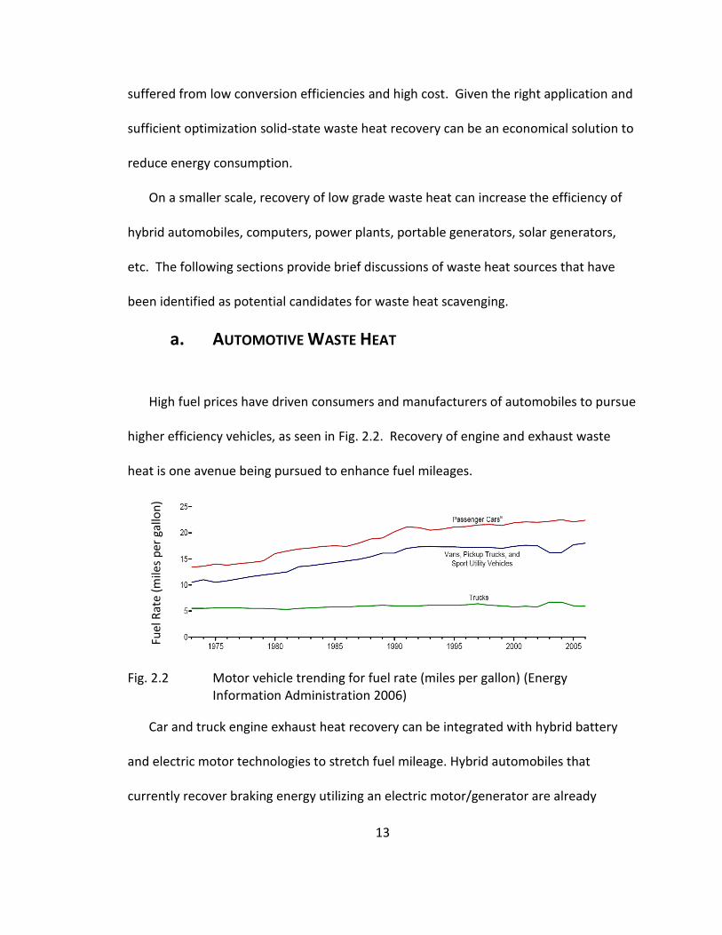
a. AUTOMOTIVE WASTE HEAT
High fuel prices have driven consumers and manufacturers of automobiles to pursue
higher efficiency vehicles, as seen in Fig. 2.2. Recovery of engine and exhaust waste
heat is one avenue being pursued to enhance fuel mileages.
Fig. 2.2 Motor vehicle trending for fuel rate (miles per gallon) (Energy Information Administration 2006)
Car and truck engine exhaust heat recovery can be integrated with hybrid battery
and electric motor technologies to stretch fuel mileage. Hybrid automobiles that
currently recover braking energy utilizing an electric motor/generator are already
Fuel
Rat
e (m
iles
per
gal
lon
)

14
performing waste heat recovery. Kinetic energy during breaking is being converted into
a stored potential energy in the form of a battery instead of generating brake heat.
Hot engine exhaust is another form of waste heat that is generated during
combustion and is typically expelled with the exhaust gases. Thermal waste heat
recovery for engine exhaust can replace the low efficiency alternator on many
automobiles. Efficient thermoelectric devices have been estimated to have the potential
to save 7.1 billion gallons of gas a year (Fairbanks 2006).
Recovery of engine waste heat could also be performed using solid-state energy
conversion. Development of waste heat recovery systems utilizing thermoelectric
power generation are currently being pursued by multiple automobile manufacturers
(Fairbanks 2006).
b. SERVER COMPONENT WASTE HEAT
An area of energy consumption that is being scrutinized is datacenter power
consumption. Datacenters are estimated to consume 1.5% of U.S. energy
consumption, which cost a total of about $4.5 billion dollars according to a U.S. Energy
Star report (ENERGY STAR program 2007). Fig. 2.3, illustrates that unless new
innovative advances in server/datacenter technology are developed and implemented
this problem will continue to grow. This thesis explores how waste heat from individual
server components can be converted directly into electricity. Component operating

15
temperatures and heat dissipation requirements are discussed here to help define the
boundary conditions of the problem.
Fig. 2.3 Historical and projected datacenter energy consumption trends (EPA 2007)
Recovered energy is used to offset energy consumption and improve process
efficiencies. In the case of computers, waste heat recovery can be used to drive fans for
the cooling system to reduce the fan power burden on the system and facility cooling
requirements. The vast majority of servers are air cooled with forced convection. This
means that the energy consumed by the server is dissipated into the air. The air is then
typically conditioned by Computer Room Air Conditions (CRAC) or Computer Room Air
Handler (CRAH) which accounts for at least half of most data center’s power budget.
The waste heat recovered from a server has at least a 2X effect on power
consumption at the datacenter level. First, generation of electricity replaces a portion

16
of the power that would have been consumed from the grid by the server. Second, that
heat that was converted to electricity no longer has to be removed by the CRACs or
CRAHs. Lastly, there will be smaller losses in datacenter and server power distribution
due to the reduced load. Therefore, recovery of server waste heat impacts more than
just the individual server power consumption and may lead to more than a 2 watt
power savings for every 1 watt of recovered power.
The power consumption of individual server components can range from 0-150W.
The dominating consumers are generally the microprocessors (CPUs), memory modules,
chipset, voltage regulation components, power supplies and hard drives. The maximum
operating temperature of most server components ranges from 60°C to 150°C.
Hard drives consume as much as 20W and have a relatively low maximum allowable
temperature ~50-60°C. Hard drive densities in a server rack can range from a diskless
operation to roughly 200 hard drives in high density storage applications. Their low
operating temperatures make them a poor candidate for waste heat recovery.
CPUs consume as much as 150W and operate at junction temperatures between 60-
75°C depending on utilization and processor type. A typical server can have anywhere
from one to four separate processors. A standard 42U rack with 1U 2S servers will
contain 84 processors per rack. This means there can be over 10kW of CPU heat
dissipated per rack. It should be noted that CPUs generally have heat sinks with
retention hardware lending them to be integrated more readily with energy conversion
hardware with minimal changes to existing server hardware.

17
A single memory module consumes less than 20W of power. However, due to the
high number of memory modules available in today’s servers, a bank of memory can
consume as much or more power than a CPU. The maximum package temperature of
most memory modules is around 85-95°C. A rack of high density servers can have round
500 memory modules. The relatively high operating temperature makes an attractive
candidate for waste heat recovery. The challenge in recovering the memory waste heat
is the dispersion of power over the large surface area of the many modules.
Chipset and other various components typically dissipate under 50W and have
temperature limits of up to 125°C. Some of these components are allowed to operate
at higher maximum temperatures. However due to the variability of board layouts and
components used, a custom recovery solution would be required.
In addition to recovering waste heat, it is necessary to ensure each component
temperature is maintained at its specified value. The challenge exists in properly cooling
the component and maintaining high enough temperatures for appreciable energy
conversion. These competing requirements require a complex thermal solution. It is
necessary to integrate the converter design with a thermal solution that can manage the
operating temperature of the component without overcooling. Solbrekken, et al
(Solbrekken, Kazuaki and Bar-Cohen 2004) has shown one such implementation in his
study of waste heat recovery of CPU waste heat in a portable computer.
Thermal energy conversion requires a temperature difference across the converter
to produce useful work. Energy converters need to be cooled with the cold temperature

18
provided by the supply air from the data center cold aisle. Data centers generally
operate from 15°C to about 30°C. The temperature ranges and heat loads available in
the server/data center environment are complied in Table 2.1. These boundary
conditions will be used to determine the feasibility of implementing solid-state waste
heat recovery.
Table 2.1 Identified server component specifications
Component Approximated Operating
Temperature [°C] Approximated Heat
Dissipation [W]
CPU 60-75 150
Memory Module 85-95 20
Hard Drive 50-60 25
iii. REFERENCE CONCEPT
For sake of discussion a reference device is presented in Fig. 2.4. This is a basic
representation of the common elements of an emission based energy converter. This
basic diagram is provided as an example to provide context for future discussions on
emission and thermal modeling.
The reference device includes the typical diode configuration with emitter and
collector electrodes. The emitter is in thermal communication with the heat source and
the collector with the ambient via a heat sink. Electrons are intentionally emitted from
the emitter electrode to be “collected” by the collector electrode. Unintentional “back

19
emission” is also emitted from the collector and collected by the emitter. The net
difference between the emitter electron emission and collector “back emission” is
equivalent to the electrical current generated by the device. The electrodes are
connected electrically to a load. The voltage potential developed is dictated primarily by
the material work functions of the emitter and collector.
Thermal modeling for the reference concept includes thermal radiation exchange
between the electrodes. Thermal resistances are modeled between the heat source and
emitter as well as between the collector and ambient air. It is important to accurately
estimate the emitter and collector temperatures because electron current emission is
an exponential function of electrode temperature.

20
Fig. 2.4 Reference concept – baseline configuration
Emitter Electrode
Collector Electrode
Thermal resistance between heat source
and emitter
Electrical Load
Magnetic Field Emitted
Electrons Thermal
Radiation
TS
“Back” Emitted
Electrons
Thermal Radiation
T∞
Electric Field
Thermal resistance of collector heat sink
Rejected Heat from Collector
Source Heat
Interstitial Gap
Generator
I +
-

21
3. EMISSION PHYSICS
The term emission refers to a process of an object that is expelled, discharged or
ejected and in the context of this thesis will be used to refer to the process of electrons
being expelled from a material surface. Thermal-to-electric energy conversion is
accomplished via thermally excited electron emission currents. At first glance it may
seem that the goal of any thermal-to-electric energy conversion system would be to
maximize electric current generation. This thesis will show that it is not always best to
maximize the generated electron emission current due to inherent losses such as Joule
heating, leakage currents and space charge that reduce the efficiency of the converter.
Instead an optimization of the efficiency or net power generation of the device is
performed using a system level modeling approach.
The emitted current density can be statistically estimated using various emission
models based on a number of parameters including temperature, applied fields and
material properties. The following emission models will be based on a flat plate
electrode as illustrated in the reference concept (Fig. 2.4).
A key element of all emission models is the potential barrier that exists in the
interstitial gap between electrodes (as seen in the reference concept Fig. 2.4). The
interstitial gap can be made up of a vacuum, plasma, gas, positive ion cloud, or solid
material(s). The potential barrier is the summation of forces inhibiting the escape of an
electron from a material, thus reducing the number of emitted electrons.

22
There are two mechanisms by which an electron can overcome the potential barrier:
thermionic (TI) and tunneling emission, as suggested by Fig. 3.1. Thermionically emitted
electrons are high energy electrons that have sufficient energy to overcome the
opposing force of the potential barrier. Unlike thermionically emitted electrons,
tunneling electrons are low energy electrons that have insufficient energy to overcome
the potential barrier, but still find their way across the barrier. More detail is provided
on these mechanisms in the coming sections.

23
Fig. 3.1 Illustration of thermionic (A) and tunneling (B) emission mechanisms
i. FERMI LEVEL, WORK FUNCTION & THE POTENTIAL BARRIER
There can be multiple contributors to the magnitude of the potential barrier with
the prominent contributors being the electron’s attraction to the material lattice known
“Potential Barrier”
ΦE
Po
ten
tial
Ener
gy
ΦC
Kin
etic
Ener
gy
Ele
ctro
n E
ner
gy
Emitter Collector
Tunneling Emission
(B) Total
Electron Energy
e-
Gap
Kin
etic
Ener
gy
Po
ten
tial
Ener
gy
“Potential Barrier”
ΦE
Po
ten
tial
Ener
gy
ΦC K
inet
ic
Ener
gy
Emitter Gap Collector
e-
Thermionic Emission
(A)
Ele
ctro
n E
ner
gy
Total Electron Energy
Po
ten
tial
Ener
gy
Kin
etic
Ener
gy
24
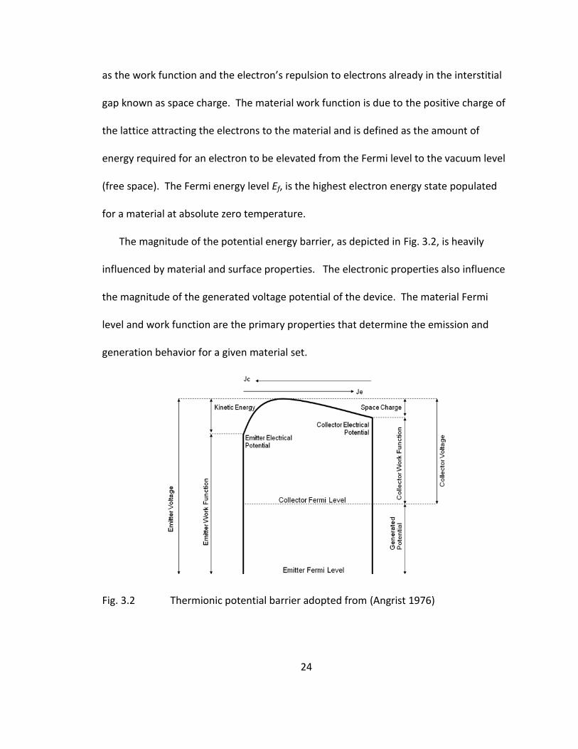
as the work function and the electron’s repulsion to electrons already in the interstitial
gap known as space charge. The material work function is due to the positive charge of
the lattice attracting the electrons to the material and is defined as the amount of
energy required for an electron to be elevated from the Fermi level to the vacuum level
(free space). The Fermi energy level Ef, is the highest electron energy state populated
for a material at absolute zero temperature.
The magnitude of the potential energy barrier, as depicted in Fig. 3.2, is heavily
influenced by material and surface properties. The electronic properties also influence
the magnitude of the generated voltage potential of the device. The material Fermi
level and work function are the primary properties that determine the emission and
generation behavior for a given material set.
Fig. 3.2 Thermionic potential barrier adopted from (Angrist 1976)

25
As stated earlier the Fermi energy level Ef, is the highest electron energy state
populated when a material is at absolute zero temperature. As the temperature of the
material increases a portion of the electrons will attain energy states above the Fermi
level. At any temperature above absolute zero the probability of the Fermi level energy
state being occupied by an electron is always 50%. The Fermi energy level Ef, is given by:
3/22
8
3
2
e
e
f
n
m
hE
3.1
where is Planck’s constant, ne is the number of electrons per unit volume, and me is
the mass of an electron. The probability of an electron being at energy E, for a given
temperature is described by the Fermi-Dirac distribution. The Fermi-Dirac distribution ff
at energy E, is given by
1exp
1)(
/)(
eBf TkEEF Ef
3.2
where kB is Boltzmann’s constant, and Te is the electron’s temperature. For
temperatures above absolute zero there is a finite probability that an electron will have
an energy greater than the Fermi level, as shown in Fig. 3.3.
h
26
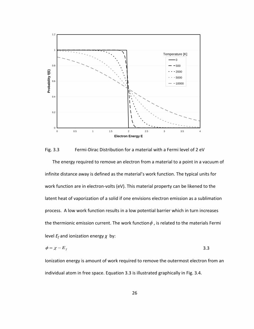
Fig. 3.3 Fermi-Dirac Distribution for a material with a Fermi level of 2 eV
The energy required to remove an electron from a material to a point in a vacuum of
infinite distance away is defined as the material’s work function. The typical units for
work function are in electron-volts (eV). This material property can be likened to the
latent heat of vaporization of a solid if one envisions electron emission as a sublimation
process. A low work function results in a low potential barrier which in turn increases
the thermionic emission current. The work function , is related to the materials Fermi
level Ef and ionization energy χ by:
fE 3.3
Ionization energy is amount of work required to remove the outermost electron from an
individual atom in free space. Equation 3.3 is illustrated graphically in Fig. 3.4.
0
0.2
0.4
0.6
0.8
1
1.2
0 0.5 1 1.5 2 2.5 3 3.5 4
Electron Energy E
Pro
bab
ilit
y f
(E)
0
500
2000
5000
10000
Temperature [K]

27
Fig. 3.4 Illustration of the relationship between ionization energy, work function and the Fermi level as described in Equation 3.3
Surface atoms are bonded differently to the lattice as compared with atoms
located in the interior of a material. The interaction between the escaping electron and
surface atoms are commonly the dominant force driving the magnitude of the work
function. To date most accurate work functions are measured empirically. Work
functions of various materials are listed in Table 3.1.
Ef

28
Table 3.1 Tabulated values of work functions for various materials
Material Material Symbol Work Function, φ
[eV] Melting Point
[°C]
Cesium Ce 2.9 798
Gold Ag 4.26 1064
Molybdenum Mo 4.6 2617
Platinum Pt 5.65 1772
Titanium Ti 4.33 1660
Tungsten W 4.55 3410
Scandate - 1.6* -
Silicon Si 4.85 1410
Silicon Carbide SiC 4.4-4.6** -
(CRC Press, Inc, 1983-1984) * Estimated based on Scandate emission measured by Gaertner et al (Gaertner, Geittner, Lydtin, & Ritz, 1997) **(Mackie, Hinricks, & Davis, 1990)
The material work function can also vary as a function of material temperature
where the work function is given by:
materialT * 3.4
where is the work function at T = 0 K, and α is the temperature coefficient
( ). Fig. 3.5 shows the variation in work function for Tungsten across a
temperature range. While the variation appears insignificant, electron emission
increases exponentially with work function which results in large changes in current
density for small variations in work function. The plot shows that a 0.18 eV increase in
work function results in a 50% reduction in current density.
*
dTd /

29
Further emission modeling in this thesis does not include work function variation
to temperature, but instead uses a conservative estimate of work function for
simplification. This leaves an opportunity to further refine the modeling efforts and
perform optimizations.
Fig. 3.5 Plot of work function temperature variation for Tungsten, and estimates for TI current densities using a fixed (T=0K) and temperature dependant work functions
ii. THERMIONIC EMISSION
Thermionic (TI) emission is an emission process used in solid state energy conversion
where electrons are typically emitted from a solid material at an elevated temperature.
0
1
2
3
4
5
6
7
8
9
10
0 500 1000 1500 2000 2500 3000
0
5
10
15
20
25
30
Wo
rk F
un
ctio
n [
eV]
Emitter Temperature [K]C
urr
ent
Den
sity
[A
mp
s/cm
^2]
Current Density (Work Function, T=0K)
Current Density (Temperature Dependant Work Function )
Constant Work Function (T=0K)
Temperature Dependant Work Function
α=6 x 10^-5

30
As previously stated, TI emitted electrons are those with enough total energy to
overcome the potential energy barrier.
Thomas Edison through his work on the light bulb was one of the early discoverers
of thermionic emission. Commonly considered the father of TI theory and recipient of
the 1928 Nobel Prize in Physics for his contribution, Owen Richardson developed an
empirical correlation for describing TI electric current density (Richardson 1921):
EB
E
Tk
e
EoTI TAJ
exp 3.5
where A0 the emission constant and the work function are material properties
specific to the emitter, and TE is the emitter temperature. This equation matched well
with empirical data, however, was not analytically derived.
Shortly thereafter GE Laboratory’s Saul Dushman corrected Richardson’s empirical
equation by fundamentally relating TI emission to evaporation of a monatomic gas
(Dushman 1923). Dushman made the assumption that the physical process of
sublimation of a monatomic gas is equivalent to that of the TI emission process.
Presuming that this assumption holds true the material work function would be
equivalent to the latent heat of vaporization. Dushman’s equation became generally
accepted and the most widely used model for estimating TI current densities and is now
well known as the Richardson-Duschman equation (Richardson 1921) (Dushman 1923).
The common form of the Richardson-Dushman equation is:
EB
E
Tk
e
ETI TAJ
exp2
0
3.6
31
The Richardson-Dushman equation assumes a Maxwellian electron energy distribution,
which limits the use of this equation to regions of high temperature. Other models for
predicting TI emission have been developed by Langmuir (Langmuir 1913) (Langmuir
1923), (Langmuir 1929), and Child (Child 1911), but are not as widely used. These
models account directly for space charge effects, but tend to overestimate current
densities.
TI emission is often likened to the thermodynamic sublimation process where a
solid is converted to a saturated gas with the addition of heat/energy. Similarly
electrons in a material are converted to an (emitted) electron gas with the addition of
the necessary amount of heat/energy. The following illustrates the derivation of the
Richardson-Dushman equation for TI emission utilizing the thermodynamic sublimation
process. Using the Clausius-Clapeyron equation, the heat of vaporization on a per-mole
basis for a monatomic gas fgh , is
fgmg
mg
mg
fg TdT
dPh 3.7
where mgP is the vapor pressure at temperature Tmg, and νfg is the difference in specific
volume between vapor and liquid. Assuming that the monatomic gas obeys the ideal gas
law and that the specific volume of gas is greater than that of a liquid:
mg
mg
mgfgdT
PdTRh
ln2
3.8
where is the universal gas constant. The heat of vaporization at standard pressure can
also be expressed as a function of Tmg (Dushman, 1923)
R

32
mgmg T
mgsolidp
T
mgvaporpfg dTcdTchh0
,0
,0
3.9
where 0h is the latent heat of the electrons at absolute zero temperature, cp,vapor is the
specific heat of the vapor at constant pressure, and cp,solid is the specific heat of the
solid. Combining equations 3.8 and 3.9 and solving for Pmg yields
CdTT
dTc
RdT
T
dTc
RTR
hP
mg
mg
mg
mg
T
mg
mg
T
mgsolidpT
mg
mg
T
mgvaporp
mg
mg
0 20
,
0 20
,0 11
log
3.10
where C is the constant of integration. The constant C for monatomic vapors is
(Dushman, 1923):
MCC log2
30
3.11
where is the “universal constant”, and M is the molecular weight . Units for this
constant are provided by dimensional analysis performed by Tolman (Tolman, 1920).
The specific heat of a monatomic gas is constant and is given by the relation
Rc vaporp2
5,
3.12
and the specific heat of the solid is assumed to be negligible. Therefore equation 3.10
becomes
MCTTR
hP mg
mg
mg log2
3log
2
5log 0
0
3.13
Reducing this equation and taking the exponential provides
0C

33
0
0
expexp2/52/3 CTR
h
mgmg
mgTMP
3.14
The molecular weight of an electron is given by:
eAmNM
3.15
where NA is Avagadro’s number (6.0221415 x 10²³). Equation 3.13 becomes
mgoTR
h
mg
C
eAmg TmNP
0
expexp2/52/3
3.16
and the current density JTI, is given by
enJ eTI 3.17
The kinetic theory of gases predicts that the number of electrons ne, incident on a unit
area of material is given by
EBe
Ee
Tkm
Pn
2
3.18
Assuming
3.19
3.20
then
E
o
TR
h
E
B
C
eATI eT
k
emNJ
22/3
2
exp 0
3.21
Comparing Equation 3.21 with the Richardson-Dushman equation (equation 3.6) yields
the following relation:

34
3.22
This relationship illustrates the similarity between enthalpy and work function. Both
are a measure of the energy required for a particle, be it a monatomic particle or an
electron, to be released from a solid material. The gas constant is equivalent to the
Boltzmann constant, but is expressed on per molar as opposed to per particle basis as
illustrated by:
3.23
The emission constant A0 for a material is defined as:
3
24
0
16
emkA eB
3.24
where is the reduced Plank constant.
Other forms of the derivation have been presented by (Angrist 1976), (Waterman
1924), (Dushman 1923), (Soo 1962), and (Richardson 1921). The Richardson-Dushmann
equation (equation 3.6) can be derived using other techniques including statistical
thermodynamics.
To obtain significant electron emission, and hence electric current the emitter must
be held at a high temperature (on the order of 1000’s K) and have a relatively low work
function. Fig. 3.6 shows the electron current density as estimated by the Richardson-
Dushman Equation 3.5 for thermionic emission as a function of temperature and work
function. The plot illustrates that at low temperatures thermionic emission will be
negligible unless lower work functions are achieved. Appreciable power generation at
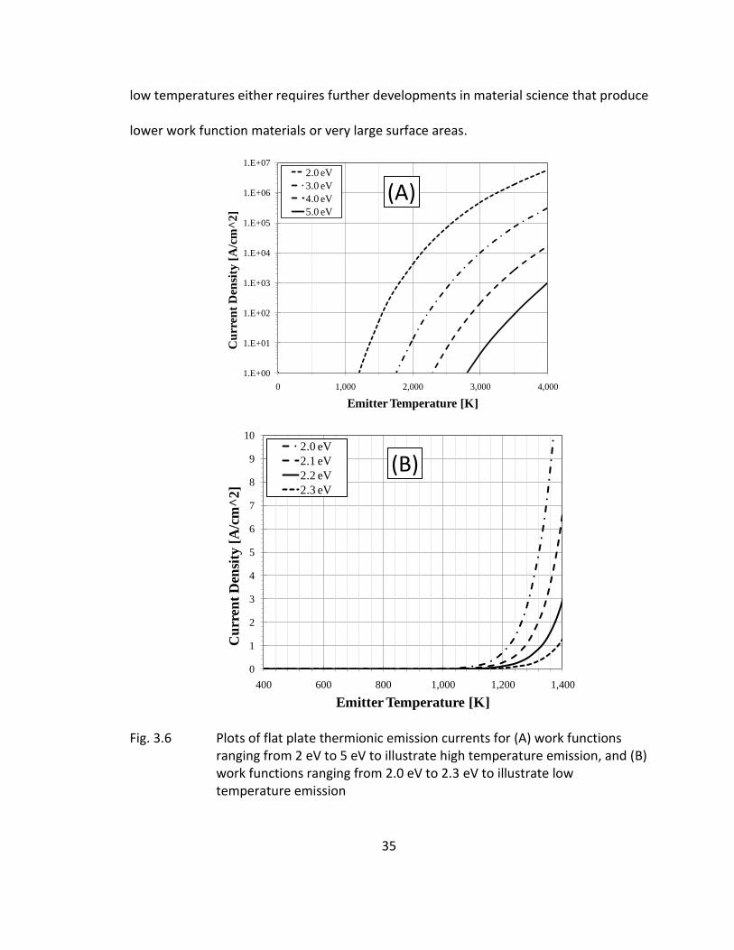
35
low temperatures either requires further developments in material science that produce
lower work function materials or very large surface areas.
Fig. 3.6 Plots of flat plate thermionic emission currents for (A) work functions ranging from 2 eV to 5 eV to illustrate high temperature emission, and (B) work functions ranging from 2.0 eV to 2.3 eV to illustrate low temperature emission
1.E+00
1.E+01
1.E+02
1.E+03
1.E+04
1.E+05
1.E+06
1.E+07
0 1,000 2,000 3,000 4,000
Cu
rren
t D
ensi
ty [
A/c
m^
2]
Emitter Temperature [K]
2.0 eV
3.0 eV
4.0 eV
5.0 eV
0
1
2
3
4
5
6
7
8
9
10
400 600 800 1,000 1,200 1,400
Cu
rren
t D
ensi
ty [
A/c
m^
2]
Emitter Temperature [K]
2.0 eV
2.1 eV
2.2 eV
2.3 eV
(A)
(B)

36
Power generation devices based on TI emission include the cesium diode (Angrist
1976), magnetic triode (Hatsopoulos and Gyftopoulos 1973) and superlattice (Mahan
and Woods 1998), (Shakouri and Bowers 1997) among others.
iii. TUNNELING
As the previous section on TI emission highlighted, only high energy electrons can be
thermionically emitted. Electrons with insufficient energy can also be emitted via a
mechanism known as tunneling. Classical mechanics predict that an electron with an
energy level less than the potential energy barrier cannot escape the emitter material or
penetrate the barrier and suggests that all such electrons will be reflected by the
barrier. However, quantum mechanics developed in the late nineteenth and early
twentieth century predicts a finite probability that a low energy electron can “tunnel”
though the potential barrier as seen in Fig. 3.1.
The probability of tunneling is formulated by considering a thin potential barrier as
illustrated in fig 3.7. Consider electrons in Region I of the figure that have higher
potential energy than the barrier. The electron can freely travel from Region I, through
Region II into Region III. As previously discussed, this is the TI emission process.
Now assume that electrons with lower potential energy than the barrier exist in
Region I of Fig. 3.7. As stated previously, these electrons cannot thermionically traverse
the barrier, but have a finite probability of tunneling through the barrier based on

37
quantum physics. The Schrodinger’s one dimensional time independent wave equation
can be solved for the three regions to determine the probability of tunneling.
Fig. 3.7 Theoretical thin potential barrier
This finite probability has been experimentally validated and is generally accepted as
a fundamental behavior of nature. It should be noted that both classical and quantum
mechanics predicts and accounts for higher energy thermionic electron emission.
The probability of an electron tunneling is a function of the potential barrier and its
magnitude. The chances for tunneling decrease as the potential energy barrier becomes
wider. The profiles for the potential barriers vary in shape and size and can be
influenced by electric field, electrode material selection and the makeup of the
interstitial gap. The potential barrier profile for tunneling emission from a flat plate
(refer to the reference concept Fig. 2.4) is more accurately given by V(x) (Hishinuma,
Geballe, & Moyzhes, 2001):
Potential Barrier
x=0 x=a
Region I Region II Region III

38
age
n
fieldE
biasndxdn
nd
xE
e
d
xV
exV
Im
1222
0
1
2
1
4
1
4)(
3.25
where the voltage difference between the emitter and collector (or gate in the
case of field emission), is the distance from the emitter surface, is the permittivity
of free space and is the distance between electrodes. An example voltage profile for a
flat plate is illustrated in Fig. 3.8. The figure illustrates how the electric field reduced the
potential barrier height, and changes the profile shape. In the absence of an electric
field (i.e. pure tunneling) the image force (or space charge) defines the potential barrier
profile.
Fig. 3.8 Flat plate potential barrier example
-20-19-18-17-16-15-14-13-12-11-10
-9-8-7-6-5-4-3-2-10
0 10 20 30 40 50 60 70 80 90 100
Po
ten
tial
[eV
]
Distance X, [nm]
Resultant Potential Barrier
Image Force Component
ф = 4.4 eV
39
a. FIELD EMISSION
Applying an electric field to the emitter material to enhance tunneling emission is a
method known as field emission (FE). This process requires a gate electrode to apply the
electric field that effectively thins the potential barrier. This thinning of the barrier
increases the probability of tunneling electron currents. FE electrons are emitted via the
tunneling process and are therefore at a lower energy state than TI electrons. Current
display technologies rely upon field emission as a source of electrons.
Low temperature or “cold cathode” field emission is possible with use of an
externally applied electric field via a gate electrode at the emission site (Nation, et al.
1999) which thins the potential barrier and increases the probability of tunneling
currents. Modeling of field emission has been performed and is classically derived as
follows.
Cold cathode field emission current density FEJ , can be estimated using probability
distributions:
0
, xbiasxxFE dEVEDENeJ 3.26
where xEN is the electron supply function, biasx VED , is the barrier transparency
function (or transmission function), biasV is the applied voltage between the emitter and
collector, and xE is the electron energy normal to the surface (x-direction). The electron
number density is a product of the available quantum states and the probability that
that state is occupied by an electron:

40
3.27
As discussed earlier the probability that a state is occupied by an electron is dictated by
Firmi-Dirac distribution as shown in Equation 3.5.
The number density of electrons is given by (Westover & Fischer, 2006):
EB
xEBex
Tk
ETkmEN exp1ln
2)(
32
3.28
where em is the mass of an electron,
Bk is Boltzmann’s constant, TE is the temperature of
the emitter surface, xE is the kinetic energy in the x direction of an electron, and is
the modified Planck constant.
The tunneling transmission coefficient )( xED , is the probability that an electron at
energy xE , will pass through the potential barrier. Using the Wentzel–Kramers–Brillouin
approximation of the Schrödinger time-independent wave equation the tunneling
transmission coefficient is given by (Westover & Fischer, 2006):
2
1
)(8
exp)(2
x
x
xe
x dxExeVm
ED
3.29
where x1 and x2 are the roots of xExeV )( .
The Fowler-Nordheim (F-N) equation predicts the cold cathode electron emission in
the presence of electric fields at absolute zero temperature and is the solution for
equation 3.26. Experimental data has shown that field emission at low temperatures
(i.e. room ambient) can be closely modeled by the F-N equation for current density. The
current density JFE, for TE = 0 is

41
F
FJFE
2/37
226
1083.6exp105.1
3.30
where is the field geometrical enhancement factor and the variable F is the applied
electric field. Fig. 3.9, shows the electron current density as estimated by the Fowler-
Nordheim equation for field emission as a function of electric field and work function.
The figure illustrates that very high current densities can be achieved using cold cathode
field emission. However, this emission mechanism is not suitable for thermal-to-
electrical energy conversion since emission is not being driven or enhanced by
temperature.
Fig. 3.9 Plot of flat plate (β=1) cold cathode field emission current densities for work functions ranging from 2.1 eV to 2.3 eV
The geometric enhancement factor accounts for non flat plate geometries such
as tip emission. The electric field is concentrated at a sharp point, tip or sphere. It is
0
10
20
30
40
50
60
70
80
90
100
800 850 900 950 1,000
Cu
rren
t D
ensi
ty [
A/c
m^
2]
Electric Field [V/μm]
FE Current @ 0 K
2.0 eV
2.1 eV
2.2 eV
2.3 eV

42
therefore possible to achieve high electric fields around a sharp point with a relatively
low gate voltage. This factor is typically determined empirically (Zuber, Jensen, &
Sullivan, 2002)(Teo, et al., 2002) .
A simple model for the geometric enhancement factor of an emitter tip is
approximated by (Zuber, Jensen, & Sullivan, 2002)
3.31
where is the radius of the emitter tip.
A study by Brodie et al suggests the following geometric enhancement factor for
the spherical tip illustrated in Fig. 3.10 (Brodie & Schwoebel, 1994):
3.32
where is the radius of the outer sphere representing the gate electrode, and is the
radius of the inner sphere representing the emitter tip.
Fig. 3.10 Illustration of a (a) spherical tip emitter and gate electrodes and (b) electric field model using concentric spheres (Brodie & Schwoebel, 1994)
A more complex and accurate treatment of the geometric enhancement factor
for a microtip is provided by Zuber et al where the factor is analytically derived based on

43
a prolate-spheroidal coordinate system (Zuber, Jensen, & Sullivan, 2002). Using the
coordinate system in Fig. 3.11 the enhancement factor is given by
3.33
where 2 is the foci distance, is the tip half-angle , is an orthogonal coordinate that
defines prolate-spheriodial surfaces. The terms and can be determine from
, 3.34
and
. 3.35
Fig. 3.11 Illustration of the prolate-spheroidal coordinate system used to derive the geometric enhancement factor in equation 3.37 (Zuber, Jensen, & Sullivan, 2002)

44
The 2D Folwer-Nordheim equation can be applied to 3D structures using the
geometric enhancement factors, but due to the assumption that the emitter is at
absolute zero temperature the Folwer-Nordheim equation for emission is only
applicable for low temperature “cold cathode” emission. There exists an “intermediate
region” between cold cathode FE and TI emission as illustrated in Fig. 3.12. The so called
“intermediate region” is where a high temperature emitter in the presence of an electric
field produces what has been named thermal-field emission (TFE).

45
Fig. 3.12 Electron Transport Mechanisms: (a) Thermionic (TI), Thermal-Field (TFE), and Field (FE) Emission, (b) Approximate Energy Distributions for Emitted Electrons
b. THERMAL-FIELD EMISSION
Thermal-field emission (TFE) was first presented in a study by W. W. Dolan and W.
Dyke (Dolan and Dyke 1954). TFE is in essence field emission of electrons at above
nominal temperatures. TFE is of particular interest because it has the potential to
produce significant currents at considerably lower temperatures than TI emission.
Ele
ctr
on
Ene
rgy
Distance from
emitter surface
0
TI
TFE
FE
Energ
y D
istr
ibution
Vacuum Level
0 K
1000 K
3000 K
Emitter Temperature
Gap Potential
Distribution
(a) (b)

46
Unlike the Fowler-Nordheim model the solution for TFE includes the emission
temperature. Solving the probability distribution integrals for current density is more
complex when temperature effects are included.
An analytic model approximating TFE is presented by (Murphy and Good Jr. 1956).
The thermal-field emission current density , is defined by the analytic model:
3.36
where the scaling factor must be less than 5 and is defined as:
3.37
where is defined as:
3.38
and is defined as:
3.39
The Nordheim elliptical function is given by:
3.40
where
3.41

47
3.42
3.43
and
3.44
To a good approximation can be given by:
3.45
Equation 3.45 is plotted for various work functions and electric fields in Fig. 3.13. The
plot illustrates that for the approximation is good for high electric fields.
Fig. 3.14 shows the TFE approximation, using the approximation given by equation
3.45, plotted as a function of electric field and work function for a given emitter
temperature of 400K. Similarly, Fig. 3.15 shows the TFE approximation plotted as a
function of emitter temperature and work function for a given applied field of 800 V/μm
(or 8x10⁶ V/cm). The figures illustrate that significant current densities can be achieved
at relatively low temperatures. For this reason TFE conversion is believed to have a
distinct advantage over TI conversion.

48
Fig. 3.13 Plot of approximated ω values based on equation 3.45 at constant temperature 400 K
0.0E+00
2.0E-03
4.0E-03
6.0E-03
8.0E-03
1.0E-02
1.2E-02
500 550 600 650 700
ωvalu
e
Electric Field [V/μm]
2 eV
3 eV
4 eV
5 eV

49
Fig. 3.14 Plot of thermal field emission current densities for various work functions
(2.0 – 2.3 eV) with respect to applied electric field
0
10
20
30
40
50
60
70
80
90
100
800 850 900 950 1,000
Cu
rren
t D
ensi
ty [
A/c
m^
2]
Electric Field [V/μm]
TFE Current @ 400 K
2.0 eV
2.1 eV
2.2 eV
2.3 eV
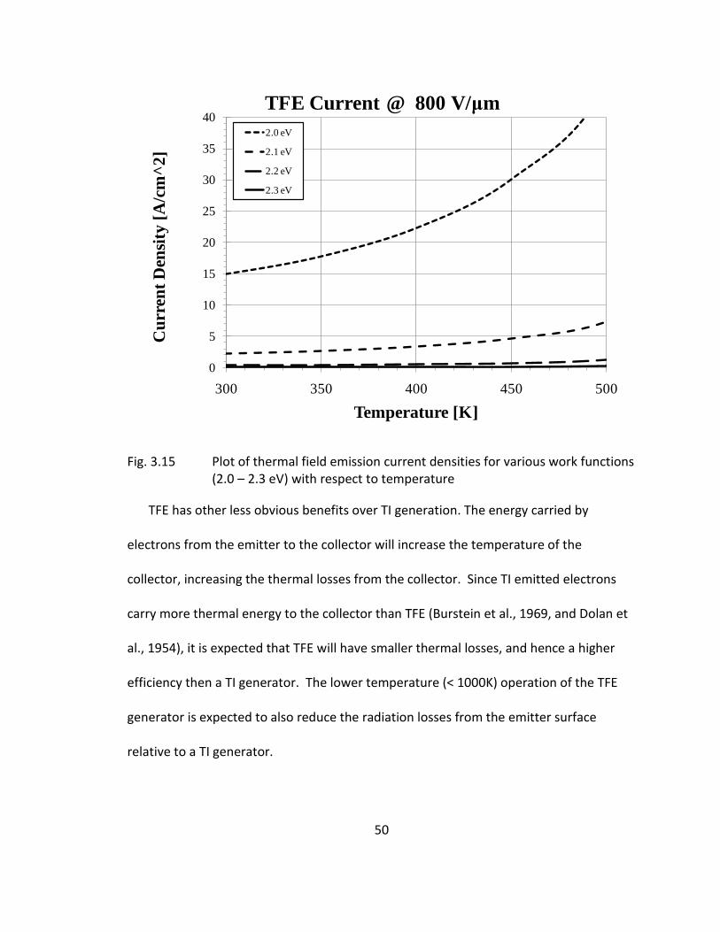
50
Fig. 3.15 Plot of thermal field emission current densities for various work functions (2.0 – 2.3 eV) with respect to temperature
TFE has other less obvious benefits over TI generation. The energy carried by
electrons from the emitter to the collector will increase the temperature of the
collector, increasing the thermal losses from the collector. Since TI emitted electrons
carry more thermal energy to the collector than TFE (Burstein et al., 1969, and Dolan et
al., 1954), it is expected that TFE will have smaller thermal losses, and hence a higher
efficiency then a TI generator. The lower temperature (< 1000K) operation of the TFE
generator is expected to also reduce the radiation losses from the emitter surface
relative to a TI generator.
0
5
10
15
20
25
30
35
40
300 350 400 450 500
Cu
rren
t D
ensi
ty [
A/c
m^
2]
Temperature [K]
TFE Current @ 800 V/μm
2.0 eV
2.1 eV
2.2 eV
2.3 eV

51
The TFE modeling equations 3.36 through 3.45 describes a temperature dependant
modification factor to FE. FE emission does not convert thermal energy into electricity
and it is assumed that all energy transferred due to FE is balanced by energy consumed
by the gate electrode to produce the electric field. Therefore, the net power generation
and thermal energy conversion is only due to the additional electron current produced
by TFE enhancement.
iv. EMISSION COMPARISON
Studies by Dolan, Dyke, Murphy and Good compare TI, TFE, and FE emission (Dolan
& Dyke, 1954)(Murphy & Good Jr., 1956). The study by Dolan and Dyke illustrates that
the three different emission types occur at different levels of the potential barrier. This
is shown in Fig. 3.16, by plotting the electron number density on the left at 0°C, 1000°C
and 3000°C correlating to FE, TFE, and TI emission temperatures, respectively. On the
right hand side of the figure the potential barrier is plotted and broken up into the three
regions of emission.
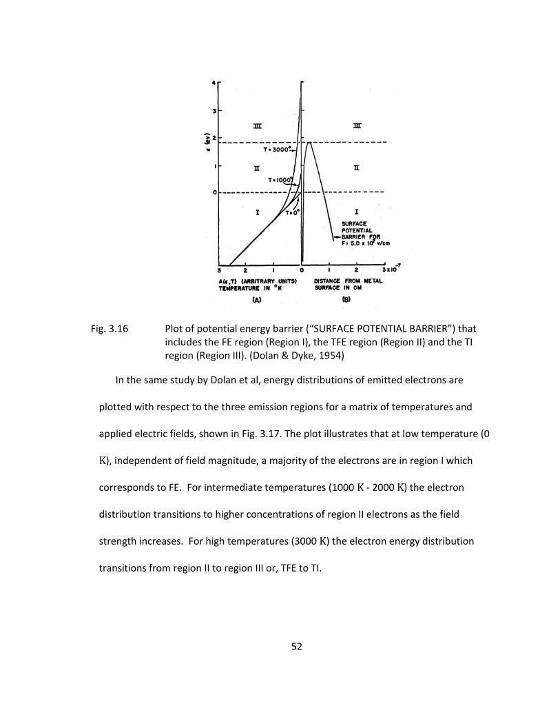
52
Fig. 3.16 Plot of potential energy barrier (“SURFACE POTENTIAL BARRIER”) that includes the FE region (Region I), the TFE region (Region II) and the TI region (Region III). (Dolan & Dyke, 1954)
In the same study by Dolan et al, energy distributions of emitted electrons are
plotted with respect to the three emission regions for a matrix of temperatures and
applied electric fields, shown in Fig. 3.17. The plot illustrates that at low temperature (0
K), independent of field magnitude, a majority of the electrons are in region I which
corresponds to FE. For intermediate temperatures (1000 K - 2000 K) the electron
distribution transitions to higher concentrations of region II electrons as the field
strength increases. For high temperatures (3000 K) the electron energy distribution
transitions from region II to region III or, TFE to TI.

53
Fig. 3.17 Plots of the energy distributions for emitted electrons at various temperatures and applied electric fields (Dolan & Dyke, 1954)
In a different study, Murphy et al shows for a given temperature and electric field
the regions where TI, TFE and TE are dominant, as shown in Fig. 3.18, where TFE is
referred to as the “Intermediate Region”. Murphy’s regions are in relative agreement
with the emitted electron energy distributions shown in Fig. 3.17.

54
Fig. 3.18 Plot of the three emission regions as a function of temperature and electric field (Murphy & Good Jr., 1956)
v. SPACE CHARGE
TI, FE, and TFE can all be impeded by space charge effects. Space charge is an
inhibiting force on electron emission caused by electron screening in the interstitial gap.
This phenomenon has an additive effect on the magnitude of the potential barrier, but
there are several methods of reducing space charge such as introducing positive ions
into the gap or decreasing the distance between the emitter and collector.
As electrons are emitted into the inter-electrode gap a “space charge” develops due
to the electrons in transit from the emitter to the collector. The space charge causes a
repulsive effect on the electrons still in the material. The electrons must overcome both
the attractive forces of the lattice (work function) and repulsive forces of the space
charge. If no emission has occurred and hence no electrons are present in the
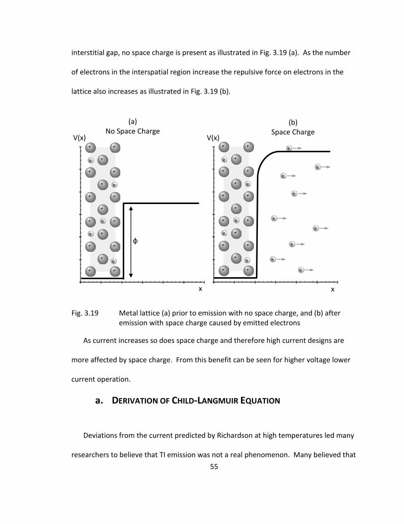
55
interstitial gap, no space charge is present as illustrated in Fig. 3.19 (a). As the number
of electrons in the interspatial region increase the repulsive force on electrons in the
lattice also increases as illustrated in Fig. 3.19 (b).
Fig. 3.19 Metal lattice (a) prior to emission with no space charge, and (b) after emission with space charge caused by emitted electrons
As current increases so does space charge and therefore high current designs are
more affected by space charge. From this benefit can be seen for higher voltage lower
current operation.
a. DERIVATION OF CHILD-LANGMUIR EQUATION
Deviations from the current predicted by Richardson at high temperatures led many
researchers to believe that TI emission was not a real phenomenon. Many believed that
e-
e-
e-
e-
e-
e-
e-
e-
e-
+ +
+
+ +
+
+ +
+
+ +
+
+ +
+
+ +
e-
e-
e-
e-
e-
+ +
+
+ +
+
+ +
+
+ +
+
+ +
+
+ +
e-
e-
e-
e-
e-
(a) No Space Charge
(b) Space Charge
V(x) V(x)
x x
ф

56
the source of the electrons was a result of chemical reactions occurring between the
electrodes and interspatial gases. This belief was backed by low currents when emission
occurred in a high vacuum. In a study by Irving Langmuir (Langmuir 1913) it was
determined that the real culprit of the reduced current was a space charge build up due
to electrons in the interspatial region. At low temperatures emission followed
Richardson’s predictions, as illustrated in Fig. 3.20. When current reached some critical
point, space charge build up was sufficient to reduce the emission and resulted in a
plateau. As higher voltage was applied to the collector the current was allowed to follow
Richardson’s prediction until the current reached a new critical point.
Fig. 3.20 Langmuir’s findings for current at various emitter temperatures and collector voltages with a gap of 1.2 cm (Langmuir 1913)
Space Charge Limited
As Predicted
by Richardson

57
At high vacuums no gases are present to counter the charge of the electrons.
Langmuir’s study illustrated that that current could be increased by increasing the
voltage of the collector, decreasing the interspatial distance between electrodes or
increasing the area of the collector.
The following is a derivation of the Child-Langmuir equation for space charge limited
electron emission. First, consider two electrodes separated by some distance d, where a
vacuum is present in between electrodes, as illustrated in Fig. 3.21. The left electrode is
biased to zero voltage and is elevated to a temperature such that appreciable electrons
are thermionically emitted. The right electrode is biased to a positive voltage, and held
at nominally room temperature, such that there is no appreciable electron emission.
The assumption is made that emitted electrons have no initial velocity.
Fig. 3.21 Case for derivation of Child-Langmuir space charge model
x-direction x = 0
V = 0
x = d
V = V
A
B
Th
Tc
Vacuum
58
From the Poisson equation:
42
2
2
2
2
22
z
V
y
V
x
VV
3.46
where V is the potential at distance x from plate A, x refers to the x-direction as
illustrated in the figure, y is the y-direction, z is the z-direction, and ρ is the space charge
density. Assume that no emission occurs in the y and z directions and the equation
reduces to:
42
2
dx
Vd
3.47
The kinetic energy of an electron traveling in the x-direction is given by:
Vevme 2
2
1
3.48
where v is the velocity of the electron. The current density J , is given by:
vJ 3.49
v is eliminated from the preceding equations as follows:
ee m
VeJ
m
Vev
22
3.50
thus
em
Ve
J
dx
Vd
24
2
2
3.51
Some algebra yields:

59
V
J
e
m
dx
Vd e22
2
2
3.52
Both sides are now multiplied by dV/dx and integrated with respect to x from 0 to d
to yield:
CJe
Vm
dx
dV e
28
2
3.53
where C is a constant. At the point x = 0, the potential distribution is horizontal
0
2
0
xdx
dVC
3.54
If the distribution where not horizontal the system would not be in equilibrium.
Therefore,
Je
Vm
dx
dV e28
2
3.55
which if integrated and solved for current density JC-L results in:
2
2/3
9
2
d
V
m
eJ
e
LC
3.56
known as the Child-Langmuir equation. This model is accurate for cases when the
thermionically emitted electron’s velocity is negligible compared to the velocity
produced by the voltage potential between electrodes. The initial velocities can be
predicted based upon a Maxwellian distribution given by:
2/1
8
e
EB
m
Tkv
3.57

60
Fig. 3.22 shows the voltage required for the electron initial and potential voltage
induced velocities to be equivalent. As previously stated Equation 3.56 is accurate when
the initial velocities are negligible compared to those induced by the potential voltage.
The figure also shows the voltage required for the potential voltage velocity to me an
order of magnitude larger than the initial velocities. The magnitude of these voltages
indicates that the Child-Langmuir equation is accurate when the voltage potential is on
the order of a volt.
Fig. 3.22 Plot illustrating the voltage required for the initial velocity to equal the potential voltage induced velocity at a given temperature, and the voltage required for the initial velocity to be one order of magnitude less (negligible) than the potential voltage induced velocity for a given temperature
0
0.5
1
1.5
2
2.5
0 500 1000 1500 2000
Po
ten
tial
Vo
ltag
e [
V]
Temperature [K]
Initial Velocity = Induced Velocity One Order of Magnitude
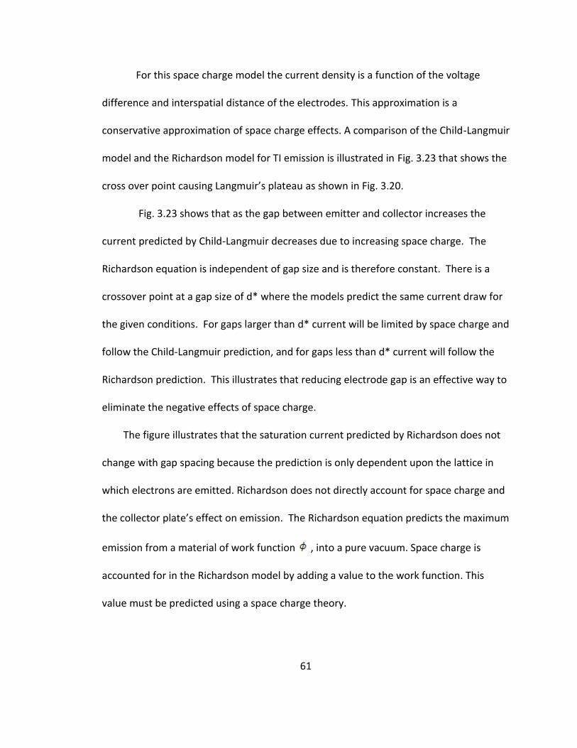
61
For this space charge model the current density is a function of the voltage
difference and interspatial distance of the electrodes. This approximation is a
conservative approximation of space charge effects. A comparison of the Child-Langmuir
model and the Richardson model for TI emission is illustrated in Fig. 3.23 that shows the
cross over point causing Langmuir’s plateau as shown in Fig. 3.20.
Fig. 3.23 shows that as the gap between emitter and collector increases the
current predicted by Child-Langmuir decreases due to increasing space charge. The
Richardson equation is independent of gap size and is therefore constant. There is a
crossover point at a gap size of d* where the models predict the same current draw for
the given conditions. For gaps larger than d* current will be limited by space charge and
follow the Child-Langmuir prediction, and for gaps less than d* current will follow the
Richardson prediction. This illustrates that reducing electrode gap is an effective way to
eliminate the negative effects of space charge.
The figure illustrates that the saturation current predicted by Richardson does not
change with gap spacing because the prediction is only dependent upon the lattice in
which electrons are emitted. Richardson does not directly account for space charge and
the collector plate’s effect on emission. The Richardson equation predicts the maximum
emission from a material of work function , into a pure vacuum. Space charge is
accounted for in the Richardson model by adding a value to the work function. This
value must be predicted using a space charge theory.

62
Fig. 3.23 Comparison of the Child-Langmuir model with the Richardson model
A more accurate model that includes initial velocities is presented by Langmuir.
Much of the work was performed by E. Q. Adams, and presented by Langmuir. The
Langmuir theory that includes initial velocities is dependent upon the emitter
temperature TE as given by:
2
231210728.7
d
TJ E
3.58
This is a more liberal estimate of space charge limited current density.
Fig. 3.24, illustrates the over prediction of the Langmuir theory for low
temperatures. At these temperatures the current follows the Richardson model
because the current emission is limited by work function. Beyond the cross over point
of the models space charge dominates and the current saturates and follows the
Child-Langmuir Law: Space Charge
1
10
100
1000
10000
100000
1000000
10000000
100000000
0 100 200 300 400 500 600 700 800 900 1000
d [nm]
I [A
mp
s]
Child-Langmuir
Richardson-Dushmann
d*
V = 0.5 V
T = 1500 K
Φc+δ = 1.3 eV
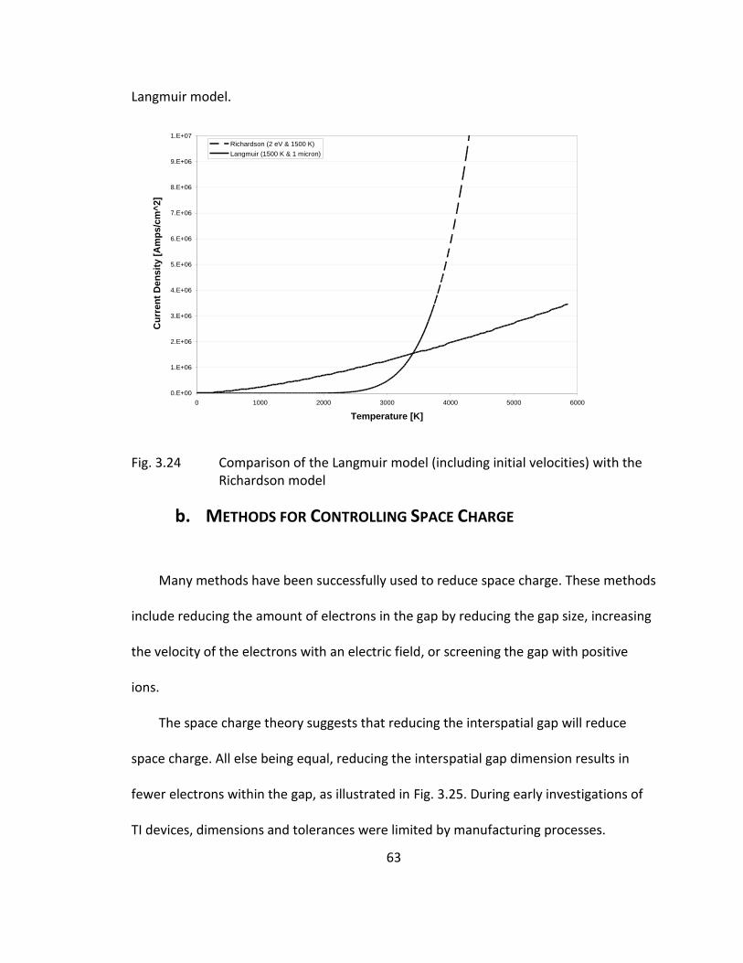
63
Langmuir model.
Fig. 3.24 Comparison of the Langmuir model (including initial velocities) with the Richardson model
b. METHODS FOR CONTROLLING SPACE CHARGE
Many methods have been successfully used to reduce space charge. These methods
include reducing the amount of electrons in the gap by reducing the gap size, increasing
the velocity of the electrons with an electric field, or screening the gap with positive
ions.
The space charge theory suggests that reducing the interspatial gap will reduce
space charge. All else being equal, reducing the interspatial gap dimension results in
fewer electrons within the gap, as illustrated in Fig. 3.25. During early investigations of
TI devices, dimensions and tolerances were limited by manufacturing processes.
0.E+00
1.E+06
2.E+06
3.E+06
4.E+06
5.E+06
6.E+06
7.E+06
8.E+06
9.E+06
1.E+07
0 1000 2000 3000 4000 5000 6000
Temperature [K]
Cu
rren
t D
en
sit
y [
Am
ps/c
m^
2]
Richardson (2 eV & 1500 K)
Langmuir (1500 K & 1 micron)

64
Current state of the art technologies allow for devices to be built on the nanoscale with
much tighter tolerances.
Fig. 3.25 Space charge control utilizing narrow gap dimensional constraint
Reducing the interspatial gap beyond a certain point will result in a finite probability
of tunneling currents. Tunneling may prove to be advantageous in power generation;
however, if the device is being used for cooling application tunneling will result in a
reduction in the effectiveness of the device as illustrated in a study by (Hishinuma,
Geballe and Moyzhes 2001). For cooling purposes it is important to remove only the
high energy electrons that carry more heat.
Another method commonly used is introducing ionized particles into the gap to
reduce the negative charge, as shown in Fig. 3.26. A common gas utilized in this method
is cesium for its low work function. Issues related to this method include supply of
positive ions to the gap, surface ionization, and electron scattering, (Angrist 1976).
A
Th
B
Tc
Wide Gap
e-
e-
e-
e-
e-
A
Th
Narrow Gap
e-
e-
e-
B
Tc

65
Fig. 3.26 Space charge control utilizing positive ions
Electric fields have successfully reduced space charge using a separate accelerating
electrode sometimes referred to as a gate electrode as illustrated in Fig. 3.27. The
primary limitation for using an accelerating electrode is the loss of power due to
electrons being inadvertently collected by the high voltage electrode (Hatsopoulos &
Gyftopoulos, 1973).
Fig. 3.27 Space charge control using a gate electrode
A
Th
B
Tc
e-
e-
e-
e-
e-
e-
e-
e-
e-
e-
Accelerating Electrodes
A
Th
B
Tc
Wide Gap
e-
e-
e-
e-
e-
+
+
+
+
+
+
+

66
Table 3.2 provides a summary of the space charge models.
Table 3.2 Space charge model summary
Model Equation Description
Richardson-Dushman
EBTk
e
ETI eTAJ
2
0
This model does not directly account for space charge, but space charge is sometimes modeled by adding an empirically derived value to the work function. The model provides a good estimate of emission when not space charge limited.
Child-Langmuir 2
2/3
9
2
d
V
m
eJ
e
This model over estimates emission when not space charge limited, but accurately describes emission when limited by space charge.
Langmuir 2
231210728.7
d
TJ E
This model also over estimates emission when not space charge limited, but to a less extent.

67
4. INTEGRATION OF EMISSION BASED DEVICE INTO A SYSTEM
i. THERMODYNAMIC BACKGROUND
Metrics are needed to compare the relative performance of a power generation
device or design. Unfortunately the electron emission studies to date have focused
primarily on maximizing current generation with little focus on device efficiency. For this
reason this thesis with use thermodynamic efficiencies to evaluate the proposed
devices.
Energy conversion efficiencies are a function of the required input to achieve the
desired output of the system. In the case of a solid state electrical generator the input
would be the heat source and the output is the generated electrical power. The first law
efficiency is given by:
in
elecricalI
Q
W
input
output
4.1
where Welectrical is the generated electrical power and Qin is the heat source input to the
system. The highest conversion efficiency is achieved for high amount of generated
electricity for a small amount of heat input.
Carnot cycle heat engines cannot achieve 100% efficiency for low temperature
power generation. The second law of thermodynamics requires that the power
generation device operate between two temperature reservoirs and that it is impossible
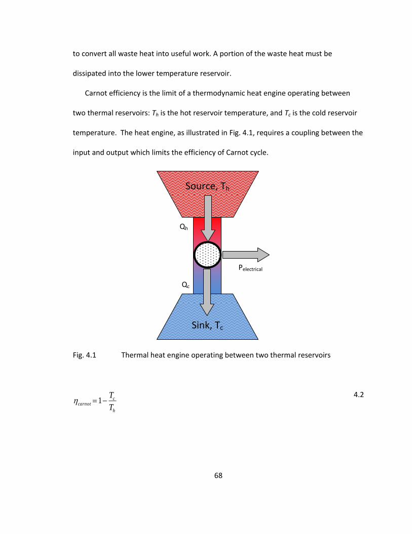
68
to convert all waste heat into useful work. A portion of the waste heat must be
dissipated into the lower temperature reservoir.
Carnot efficiency is the limit of a thermodynamic heat engine operating between
two thermal reservoirs: Th is the hot reservoir temperature, and Tc is the cold reservoir
temperature. The heat engine, as illustrated in Fig. 4.1, requires a coupling between the
input and output which limits the efficiency of Carnot cycle.
Fig. 4.1 Thermal heat engine operating between two thermal reservoirs
h
ccarnot
T
T1
4.2
Source, Th
Sink, Tc
Qh
Qc
Pelectrical

69
The total achievable efficiency goes up with an increase in the temperature delta
between the two reservoirs. A first law efficiency does not take into account this Carnot
limit, however, the second law efficiency given by:
carnot
III
4.3
is a more representative way to compare efficiencies of a system because it is based on
the Carnot limit. A highly efficient Carnot device may be misconstrued as a low
efficiency device if the first law efficiency is not compared against the Carnot limit.
Solid state energy conversion follows the Carnot heat cycle and is subject to its
limitations. The preceding efficiency discussions will be used in future sections to
evaluate and benchmark device performance and effectiveness.
ii. MAGNETIC DIODE
a. SYSTEM DESCRIPTION
The first device proposed in this thesis utilizes a magnetic field to alter
thermionic emission to reduce thermal radiation exchange between emitter and
collector. It will be shown that reducing this exchange enables lower collector
temperatures and back emission which improves conversion efficiencies. Fig. 4.2 is a
simple diagram of the device illustrating the unique electrode orientation employed.
The following sections will explain the thermal radiation exchange between the
electrodes and the system level enclosure modeling approach.

70
Fig. 4.2 Simplified magnetic diode
b. THERMAL RADIATION VIEW FACTOR
Thermal radiation exchange between emitter and collector is a dominant source of
loss and inefficiency for a TI generator. The traditional TI diode is sufficiently modeled
by assuming all radiation leaving the face of an electrode is “seen” by the other
electrode. As discussed previously the implementation of the magnetic field allows for
unconventional electrode orientations that reduce thermal radiation exchange between
the emitter and collector. A thermal radiation view factor is used to model and account
for the radiation exchange between unconventionally oriented electrodes. This section
describes the unique contribution of using thermal radiation view factors to minimize
the thermal radiation exchange between the emitter and collector.
α
Heat Input
Heat Rejection
Magnetic Field
Emitted Electrons
Thermal Radiation
Th Tc
“Back” Emitted
Electrons Thermal Radiation
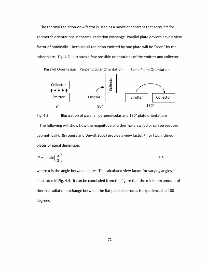
71
The thermal radiation view factor is used as a modifier constant that accounts for
geometric orientations in thermal radiation exchange. Parallel plate devices have a view
factor of nominally 1 because all radiation emitted by one plate will be “seen” by the
other plate. Fig. 4.3 illustrates a few possible orientations of the emitter and collector.
Fig. 4.3 Illustration of parallel, perpendicular and 180° plate orientations
The following will show how the magnitude of a thermal view factor can be reduced
geometrically. (Inropera and Dewitt 2002) provide a view factor F, for two inclined
plates of equal dimension:
2sin1
F 4.4
where α is the angle between plates. The calculated view factor for varying angles is
illustrated in Fig. 4.4. It can be concluded from the figure that the minimum amount of
thermal radiation exchange between the flat plate electrodes is experienced at 180
degrees.
Emitter
Collector
Parallel Orientation
Emitter
Co
llect
or
Perpendicular Orientation
Emitter Collector
Same Plane Orientation
0° 90° 180°

72
Fig. 4.4 Thermal radiation view factor for angles between emitter and collector varying from 0 to 180 degrees
It is assumed that the emitter and collector are gray bodies. The net thermal
radiation QRad,net, for the inclined plates is given by:
111
44
,
CE
CEcnetRad
TTFAQ
4.5
where AC is the cross sectional area of a plate, σ is the Stefan-Boltzmann’s Constant, εE is
the emissivity of the emitter surface, and εC is the emissivity of the collector surface.
c. ENCLOSURE MODELING
For a simple diode with a parallel orientation the view factor between the
electrodes is effectively one, and radiation exchange with other surfaces can be
neglected. However, when the plate orientation is altered to reduce this view factor
View Factor
0
0.1
0.2
0.3
0.4
0.5
0.6
0.7
0.8
0.9
1
0 20 40 60 80 100 120 140 160 180
Alpha [degrees]
Vie
w F
acto
r F
α
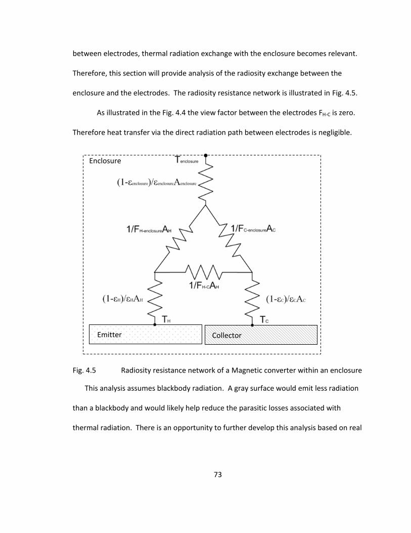
73
between electrodes, thermal radiation exchange with the enclosure becomes relevant.
Therefore, this section will provide analysis of the radiosity exchange between the
enclosure and the electrodes. The radiosity resistance network is illustrated in Fig. 4.5.
As illustrated in the Fig. 4.4 the view factor between the electrodes FH-C is zero.
Therefore heat transfer via the direct radiation path between electrodes is negligible.
Fig. 4.5 Radiosity resistance network of a Magnetic converter within an enclosure
This analysis assumes blackbody radiation. A gray surface would emit less radiation
than a blackbody and would likely help reduce the parasitic losses associated with
thermal radiation. There is an opportunity to further develop this analysis based on real
Enclosure
Emitter Collector
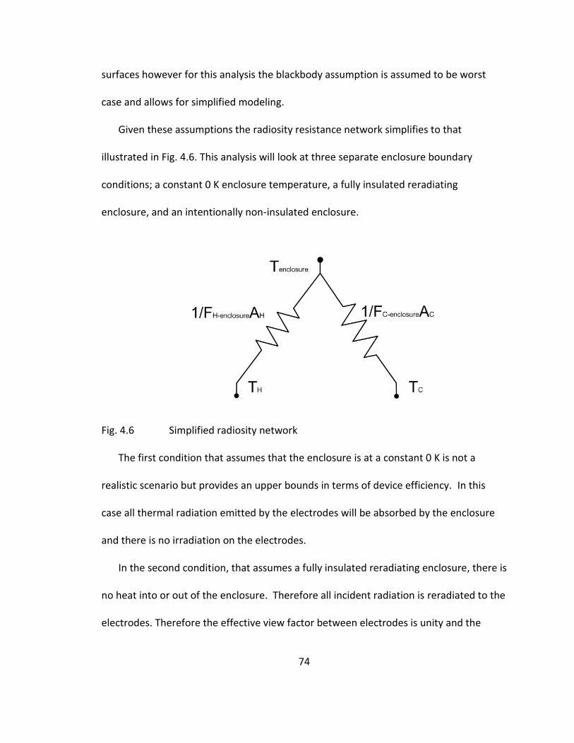
74
surfaces however for this analysis the blackbody assumption is assumed to be worst
case and allows for simplified modeling.
Given these assumptions the radiosity resistance network simplifies to that
illustrated in Fig. 4.6. This analysis will look at three separate enclosure boundary
conditions; a constant 0 K enclosure temperature, a fully insulated reradiating
enclosure, and an intentionally non-insulated enclosure.
Fig. 4.6 Simplified radiosity network
The first condition that assumes that the enclosure is at a constant 0 K is not a
realistic scenario but provides an upper bounds in terms of device efficiency. In this
case all thermal radiation emitted by the electrodes will be absorbed by the enclosure
and there is no irradiation on the electrodes.
In the second condition, that assumes a fully insulated reradiating enclosure, there is
no heat into or out of the enclosure. Therefore all incident radiation is reradiated to the
electrodes. Therefore the effective view factor between electrodes is unity and the

75
device is essentially the same as the simple diode configuration. It is evident that the
enclosure thermal resistance to ambient should be minimized to reduce radiation
exchange between the electrodes.
The last condition assuming a non-insulated enclosure that sinks to the ambient is
the most realistic scenario. In this case the enclosure temperature is not constant and
sinks to the ambient as illustrated in Fig. 4.7.
Fig. 4.7 Non-insulated enclosure radiosity network
The enclosure analysis reveals that simply reducing the view factor between
electrodes and eliminating the direct radiation path does not necessary prevent thermal
communication between the electrodes. Care must be taken in the design of the
enclosure to optimize energy conversion efficiencies. The next section proposes a
method to eliminate heat loss through the enclosure.

76
d. THERMAL RADIATION RECOVERY METHOD
Reducing the thermal radiation exchange between emitter, collector, and
enclosure will enhance both performance and efficiency by maintaining the electrodes
at optimal temperatures. Further enhancement can be obtained by recovering the
radiation losses from the emitter and preventing it from being reradiated off of the
enclosure to the collector. This can be accomplished by placing plates of nominally the
same temperature across from the emitter and collector as illustrated in Fig. 4.8.
Fig. 4.8 Thermal radiation recovery orientation
The view factors for radiation exchange between the emitter and cold plate or
the collector and hot plate are equivalent to each other. To determine this view factor
consider the resultant view factor in Fig. 4.9, where view factors plates of unequal
dimension and plates of equal dimension plates are known.
Plate @ Tc
Emitter @ Th Collector @Tc
Plate @ Th
Net Radiation
exchange ~
zero
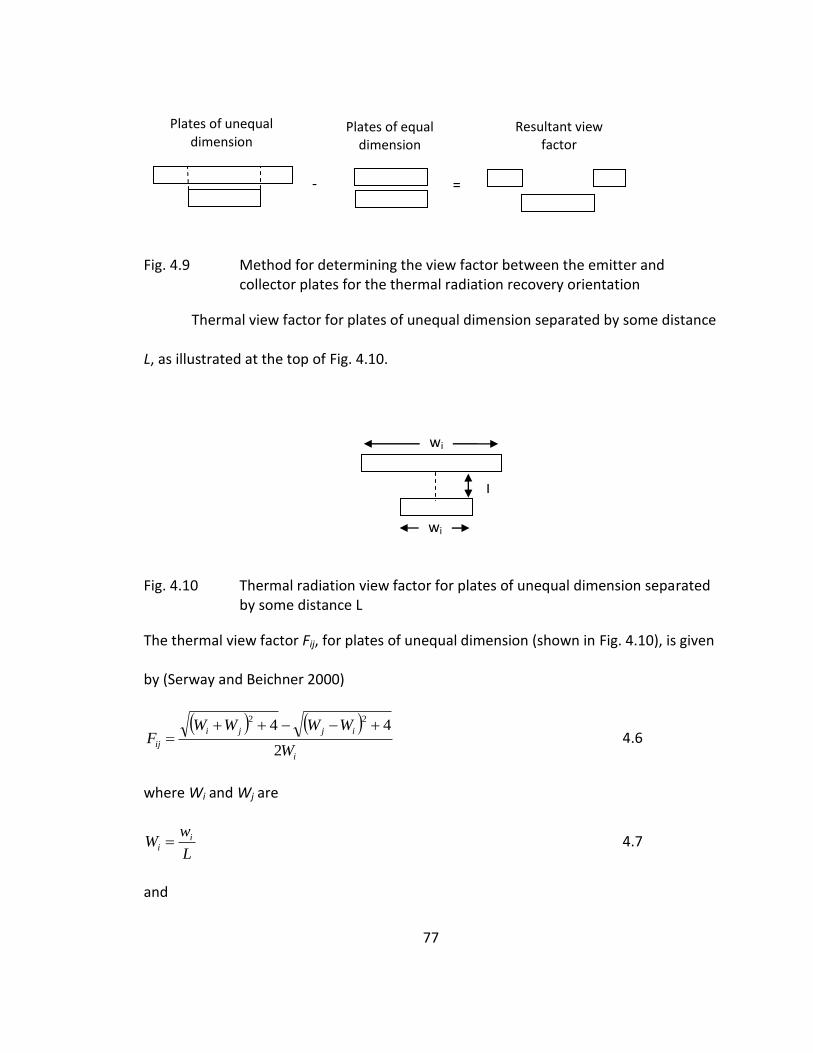
77
Fig. 4.9 Method for determining the view factor between the emitter and collector plates for the thermal radiation recovery orientation
Thermal view factor for plates of unequal dimension separated by some distance
L, as illustrated at the top of Fig. 4.10.
Fig. 4.10 Thermal radiation view factor for plates of unequal dimension separated by some distance L
The thermal view factor Fij, for plates of unequal dimension (shown in Fig. 4.10), is given
by (Serway and Beichner 2000)
i
ijji
ijW
WWWWF
2
4422
4.6
where Wi and Wj are
L
wW i
i 4.7
and
wi
L
wj
- =
Plates of unequal dimension
Plates of equal dimension
Resultant view factor

78
L
wW
j
j 4.8
respectively.
The resultant view factor is plotted at various separation distances in Fig. 4.11.
The figure illustrates that the thermal radiation exchange between the emitter and
collector can be significantly reduced in comparison with the usual diode configuration
and can be made negligible with a sufficiently small gap L. The view factor between the
hot plates as well as between the cold plates will approach unity as the gap is reduced.
Like the simple diode design there will be negligible radiation exchange with the
enclosure.
Fig. 4.11 Thermal radiation view factor for varying plate separation distances

79
iii. TFE NANOWIRE CONVERTOR
a. SYSTEM DESCRIPTION
The second proposed device utilizes TFE from nanowire emitters. Fig. 4.12 shows
a simplified diagram of the TFE nanowire convertor. The diagram shows the nanowire
emitters, gate, and collector electrodes. The following sections will describe the system
level thermal modeling approach taken for the TFE nanowire convertor.
Fig. 4.12 Simplified TFE nanowire convertor
EEEmmmiiitttttteeerrr SSSuuubbbssstttrrraaattteee
Gate
CCCooolll llleeeccctttooorrr
Insulator
Gate
Insulator
Emitter Electron Emission
Collector Back Emission
Emitter Thermal Radiation
Collector Thermal Radiation
Rejected Heat
Nanowires
Heat Source
Vacuum

80
b. THERMAL MODELING
This section will focus on thermal modeling of the TFE nanowire convertor. Many
energy conversion studies assume constant temperature boundary conditions for their
analysis of energy convertors. This type of modeling approach reduces complexity of the
model, but also reduces the accuracy of the prediction as shown with in the Magnetic
Diode example. Most real world applications typically include some level of thermal
impedance between the source and convertor. For this reason this model will include
thermal resistances between the temperature reservoir and the convertor. This
additional thermal modeling improves the accuracy between theory and practice and
allows for optimization of the converter performance based on application.
In addition to the system level modeling approach this device concept will be
modeled based on a server waste heat source to help illustrate both the benefits of
system level modeling and the applicability of recovering server waste heat.
Two types of boundary conditions are considered for the thermal model: constant
source temperature and constant source heat flux. Determining the appropriate
boundary condition is application/heat source dependant. In the case of processor
waste heat recovery application either boundary condition could effectively be used.
The processor has a relatively constant heat flux for a given stress load, but the
reliability requirements of the processor require that the processor not exceed a specific
temperature. Overcooling of the processor consumes unnecessary energy commonly in
81
the form of fan power. A shunt heat sink is used in parallel with the convertor to
regulate the processor temperature to within its operating specification. Based on the
application and source the constant heat flux boundary condition should be assumed for
a system level modeling approach. However a more myopic view of the converter
would suggest that using a constant temperature heat source would provide for
simplified modeling. In this case it is assumed that the shunt resistor is varied to
provide the necessary cooling to maintain the processor temperature specification. It is
important to ensure that the heat flux through the convertor does not exceed that
produced by the source.
c. THERMAL RESISTANCE NETWORK
The conduction, convection and radiation heat transfer for such a device is well
understood and based on fundamentals of heat transfer theory with the exception of
the emission process. A certain amount of energy will be transported from the emitter
to the collector via net electron currents. Electron emission heat transfer is modeled as
a black box. Determining how to treat the emission black box in a thermal resistance
network is not entirely explicit. Therefore the more common approach to thermal
modeling of an electron emission device is to perform separate energy balances around
the emitter and collector.
As an exercise to illustrate the thermal complexity of the device a thermal resistance
network for the TFE convertor is presented in Fig. 4.13. The network assumes that all

82
contact resistances are lumped into the various conduction resistances for
simplification.
Fig. 4.13 Detailed TFE convertor thermal resistance network
The thermal resistances shown in Fig. 4.13 figure are as follows:
ΨCond, Sub, E : Thermal conduction through the emitter substrate. The contact resistance between the substrate and the heat source is lumped into this term.
ΨCond, NW : Bulk thermal resistance of the oriented SiC nanowires.
ΨCond, Gate : Thermal conduction of the gate insulator, gate electrode, gate circuitry (which is a function of the ambient temperature, but is neglected for simplicity), and contact resistances.
ΨCond, Structural : This is the thermal resistance of the mechanical structure and housing for the device.

83
ΨCond, Circuitry : This is the thermal resistance of the electrical circuit that attaches the emitter and collector. Depending upon the magnitude of current, joule heating may occur in the lead wires of the circuitry.
ΨCond, Sub, C : Bulk thermal resistance of the collector and contact resistance between the collector and the heat sink.
ΨRad, NW : This is the thermal resistance of the thermal radiation emitted by the nanowires
ΨRad, Gate : Thermal resistance of the thermal radiation exchange between the gate and the collector.
ΨRad, Sub : This is the thermal resistance of the radiation exchange between the emitter substrate and collector surfaces.
ΨConv, SHS : This is a variable thermal resistance of the shunt heat sink designed to keep the heat source within a specified temperature range.
ΨConv, HS : The thermal resistance of the heat sink used to keep the collector cool by expelling heat transferred from the emitter.
ΨLoss : This thermal resistance represents the culmination of the remaining parasitic heat losses (such as heat loss to the ambient from the emitter directly to the ambient)
The TFE generator is illustrated in the resistance network as a “black box”. The
generator includes those elements between the emitter and collector temperatures.
The generator cannot be depicted as a thermal resistance because of the conversion of
thermal energy into electricity. A portion of the source heat will be converted into
electrical energy that is consumed at the electrical load. The remaining amount of
energy carried from the emitter to the collector will be dissipated through the collector
heat sink. The heat transfer between the emitter and collector is a result of thermal
radiation and electron emission energy exchanges.

84
There are several assumptions made in developing the thermal resistance network.
It is assumed that the device is perfectly insulated from the ambient in all areas other
than the heat sink and electrical load. This assumption will not affect the accuracy of
the model since the magnitude of this heat loss is negligible. It is also assumed that
conduction and convection within interstitial gap is negligible due to the ultra high
vacuum environment. This resistance network also assumes no power loss through the
gate circuitry. In practice there will be losses associated with emitted electrons being
inadvertently collected by the gate electrode. This will be discussed later in greater
detail.
The thermal resistance model illustrated in Fig. 4.13 is not necessary to create an
accurate thermal model for a TFE convertor. Fig. 4.14 shows a reduced network that
lumps resistances together reducing the complexity without sacrificing model accuracy.
The thermal resistance network is necessary to accurately predict the emitter and
collector temperatures which relate to electron emission and power generation.
Fig. 4.14 Simplified TFE convertor thermal resistance network
The net thermal radiation exchange between the emitter side surfaces and the
collector surface is modeled as ΨRad. Thermal radiation from the emitter substrate,
ψRad
ψCond, Sub, E ψCond, Sub, C ψHConv, HS TS T∞
TFE Emission

85
nanowires and gate are modeled as a flat plate of the same projected area and
assumed to emit thermal radiation at the emitter substrate temperature.
d. ENERGY BALANCE
To precisely model and characterize the performance and efficiency of the TFE
converter it is necessary to keep an accurate balance of all energy transactions. It is
customary to form separate control volumes around the emitter and collector or a
control volume around the interstitial gap. The following emitter and collector control
volumes and associated energy balances roughly correlate to the control volumes
indicated in the thermal resistance network shown in Fig. 4.13. This control volume
assumes the device has perfect insulation in order to neglect insignificant heat transfer
to the surroundings.
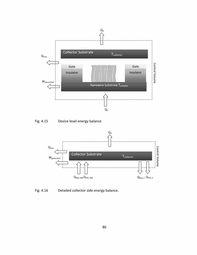
86
Fig. 4.15 Device level energy balance
Fig. 4.16 Detailed collector side energy balance.
CCCooolll llleeeccctttooorrr SSSuuubbbssstttrrraaattteee Tcollector
QTFE, NW QRad, NW QTFE, C QRad, C
Wgenerated
Co
ntro
l Vo
lum
e
QO
QLoss
CCCooolll llleeeccctttooorrr SSSuuubbbssstttrrraaattteee Tcollector
QO
NNNaaannnooowwwiiirrreee SSSuuubbbssstttrrraaattteee Temitter
Gate
Insulator
Co
ntro
l Vo
lum
e
QS
Gate
Insulator
QLoss
WGenerated

87
Fig. 4.17 Detailed emitter side energy balance
Simplified energy balances are performed around the emitter and collector, as
shown in Fig. 4.18 and Fig. 4.19 respectively. Simplification of the energy balances is
useful in performing a device feasibility study.
Fig. 4.18 Simplified collector side energy balance
Collector Tcollector
WElectrical
Co
ntro
l Vo
lum
e
QO
QTFE, E QRad, E QTFE, C QRad, C
NNNaaannnooowwwiiirrreee SSSuuubbbssstttrrraaattteee Temitter
QTFE, NW QRad, NW QTFE, C QRad, C
Gate
Insulator
Gate
Insulator
Co
ntro
l Vo
lum
e
QS

88
4.9
Fig. 4.19 Simplified emitter side energy balance
4.10
The energy carried by electrons from the emitter to the collector will increase the
temperature and thermal losses of the collector. Since TI emitted electrons carry more
thermal energy to the collector than TFE (Burstein et al., 1969, and Dolan et al., 1954)
(Dolan and Dyke 1954), it is expected that TFE will have smaller thermal losses, and
potentially a higher efficiency then a TI generator. The lower temperature (< 1000K)
operation of the TFE generator is expected to also reduce the radiation losses from the
emitter surface relative to a TI generator.
Emitter Substrate Temitter
Co
ntro
l Vo
lum
e
QS
QTFE, E QRad, E QTFE, C QRad, C
89
5. ANALYSIS OF SYSTEM
i. ITERATIVE SOLVING
Solving the energy balances, emission equations and thermal resistance networks
for the Magnetic Diode and TFE Nanowire Convertors required multiple iterations to
converge on a solution as illustrated in the flow chart in Fig. 5.1. The process required
making an initial guess of electrode temperatures to acquire first pass estimates of
emission current densities. Then the energy balance calculations are performed based
on the emission approximation to estimate new electrode temperatures. The new
electrode temperatures are used to update the emission current estimates and the
process is repeated until the temperatures converge on a solution. This iterative process
is also repeated for each unique set of emission and thermal parameters.
The iterative solution of the device models were performed using Matlab programs
and Microsoft Excel. Some of the Matlab programs used to solve the modeling can be
found in the appendix. Excel solutions required starting with constant temperature
electrodes to perform the emission current approximations. Then thermal components
of the analysis were added one by one to the calculations. Each time a component was
added Excel would reiterate until a solution was found. Once all components were
added a solution was found. Adding all thermal components at one time resulted
divergence.

90
Fig. 5.1 Flow chart illustrating iterative method used to solve electromechanical models
ii. MAGNETIC DIODE CONVERTOR
a. MAGNETIC FIELD
A magnetic field (or B-field) alters the trajectory of the emitted electrons and is
proposed in order to reduce thermal radiation losses. The force exerted on a particle FB,
by a magnetic field B, is described by the equation:
BqvFB 5.1

91
where q is the charge of the particle, and v is the velocity of the particle. The magnetic
field required to cause an electron moving at velocity v, in a straight line to an arc of
radius, r, is:
re
vmB e 5.2
Motion of an electron in the presence of a B-field into the page is illustrated in Fig. 5.2.
Fig. 5.2 Illustration of electron trajectory due to B-field
Recall that the average velocity v , of an emitted electron from a material at
temperature TE, is described by the Maxwellian distribution as provided in space charge
chapter in Equation 3.48. The Maxwell distribution is suitable when dealing with high
temperatures. A Bose-Einstein distribution is more suitable when dealing with low
temperatures.
Emitter Collector
v
FB
v
FB v
B
v
FB
FB
r
Th Tc
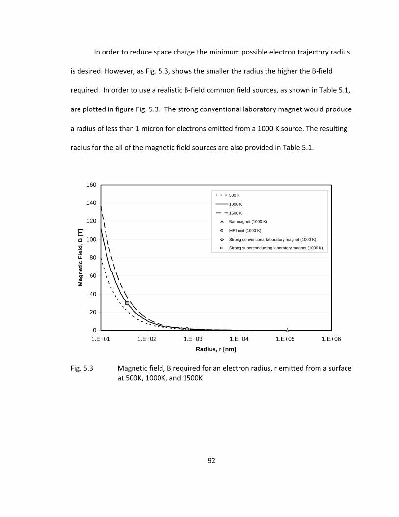
92
In order to reduce space charge the minimum possible electron trajectory radius
is desired. However, as Fig. 5.3, shows the smaller the radius the higher the B-field
required. In order to use a realistic B-field common field sources, as shown in Table 5.1,
are plotted in figure Fig. 5.3. The strong conventional laboratory magnet would produce
a radius of less than 1 micron for electrons emitted from a 1000 K source. The resulting
radius for the all of the magnetic field sources are also provided in Table 5.1.
Fig. 5.3 Magnetic field, B required for an electron radius, r emitted from a surface at 500K, 1000K, and 1500K
0
20
40
60
80
100
120
140
160
1.E+01 1.E+02 1.E+03 1.E+04 1.E+05 1.E+06
Radius, r [nm]
Mag
neti
c F
ield
, B
[T
]
500 K
1000 K
1500 K
Bar magnet (1000 K)
MRI unit (1000 K)
Strong conventional laboratory magnet (1000 K)
Strong superconducting laboratory magnet (1000 K)

93
Table 5.1 Approximate magnetic field sources (Serway and Beichner 2000)
Field Source Field Magnitude [T] Radius [nm]
Bar Magnet 10-2 105
MRI unit 1.5 745
Strong conventional laboratory magnet
2 560
Strong superconducting laboratory magnet
30 37
The first design concept explored in this thesis encompasses the use of flat plate
thermionic emission in the presence of a magnetic field. Conventional TI emission
based energy conversion devices are oriented in the traditional fashion of a diode where
electrodes are aligned face to face. The magnetic field is employed to alter the
trajectory of the electrons such that the collector can be oriented in unconventional
orientations as illustrated in Fig. 5.4. This section will show how altering the electrode
orientation can enhance conversion efficiencies.
Fig. 5.4 Collector orientations considered with the presence of a magnetic field
In a previous study, a similar concept using a magnetic field to alter electron trajectories
and electric fields to reduce space charge effects was investigated (Hatsopoulos and
Emitter
Collector
Emitter Collector
Emitter

94
Gyftopoulos 1973). A device was developed in that study that was named the
“Magnetic Triode”, and is illustrated in Fig. 5.5 that uses a magnetic “B” field to provide
the arced trajectory of the electron. The accelerating electrode is biased to a higher
voltage potential to generate an electric field that was used to reduce space charge
effects by accelerating the emitted electrons. Acceleration of the electrons removes the
electrons from the inter-electrode region faster and thus reduces the space charge.
Hatsopoulos et al found that when leakage current (i.e. stray electrons) are
inadvertently collected by the accelerating electrode, power losses on the order of that
generated are incurred (Hatsopoulos and Gyftopoulos 1973). Fig. 5.6 shows the
modeling results from Hatsopoulos’s Magnetic Triode modeling.
Fig. 5.5 Magnetic triode as adopted from (Hatsopoulos and Gyftopoulos 1973)
-
Emitter, TE Collector, TC
+ I
Va
QS QR
Vload
Accelerating Electrode
B-field

95
Fig. 5.6 Magnetic triode efficiency (Hatsopoulos and Gyftopoulos 1973)
Hatsopolous’s study showed promise in reducing both radiation losses and space
charge. However, the space charge reduction came with the tradeoff of gate leakage
current. This thesis proposes a similar design that uses extremely small dimensions to
control space charge instead of the accelerating electrode. Later modeling will also
illustrate that thermal radiation can still be transmitted from the emitter to the collector
via the accelerating electrode. This thesis will propose a method that eliminates this
heat path.
When the magnetic triode was devised the ability to dimensionally control space
charge was beyond the capability of manufacturing techniques. Today we have the
96
ability to manufacture devices at much smaller scales allowing for the control of space
charge via dimensional constraints as an alternative to the accelerating electrode.
b. SPACE CHARGE
The trajectory of the electrons must be small enough to negate the effects of space
charge. The space charge current density predicted by Childs and Langmuir is a one
dimensional model that does not account for an electron with a curved trajectory.
However it stands to reason that reducing the trajectory distance will result in a reduced
space charge.
Hatsopolous uses the same assumption in his work on the magnetic triode
(Hatsopolous, 1956), where he states, “The power output becomes appreciable only for
the very small gaps of 0.01 cm and 0.001 cm. At the present time no technique is know
by which one can obtain these small gaps in practice.” These spatial limitations drove
Hatsopolous to use an electric field to reduce space charge. Today’s technology
provides for fabrication techniques that can achieve these microscale dimensions.
The Child-Langmuir space charge and Richardson equation are plotted in Fig. 5.7 for
a work function of 2.0 eV and emitter temperature of 1000 K. Space charge becomes a
limiting factor when the Child-Langmuir predicted current is lower than that predicted
by the Richardson model. In other words the current is no longer limited by emission,
but is limited by space charge. The figure illustrates that this does not occur for
dimensions below 100 microns.

97
Fig. 5.7 Illustration of space charge limitation for an emitter at 1000 K with a work function of 2 eV
c. 1ST ORDER ANALYSIS
Many emission studies assume constant temperature boundary conditions and
neglect the effects of the enclosure. This first order model assumes no space charge,
constant temperature electrodes and an enclosure temperature of 0 K to illustrate the
problems associated with the typical emission modeling assumptions. An illustration of
these assumptions and the device configuration are provided in Fig. 5.8. Electron
emission was calculated based on the projected area of the flat plate emitter.
0
0.005
0.01
0.015
0.02
0.E+00 1.E+05 2.E+05 3.E+05 4.E+05 5.E+05
Cu
rre
nt D
en
sit
y [
A/c
m^
2]
d [nm]
Child-Langmuir Law: Space Charge
Child-Langmuir
Richardson-Dushmann
Space Charge Limited Region
Non Space Charge Limited Region Region
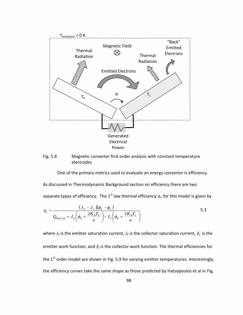
98
Fig. 5.8 Magnetic converter first order analysis with constant temperature
electrodes
One of the primary metrics used to evaluate an energy convertor is efficiency.
As discussed in Thermodynamic Background section on efficiency there are two
separate types of efficiency. The 1st law thermal efficiency ηI, for this model is given by
e
TKJ
e
TKJQ
JJ
CBEC
EBEEnetRad
CECEI
22,
5.3
where JE is the emitter saturation current, JC is the collector saturation current, E is the
emitter work function, and C is the collector work function. The thermal efficiencies for
the 1st order model are shown in Fig. 5.9 for varying emitter temperatures. Interestingly,
the efficiency curves take the same shape as those predicted by Hatsopoulos et al in Fig.
α
Generated Electrical
Power
Magnetic Field
Emitted Electrons
Thermal Radiation
Th Tc
“Back” Emitted
Electrons Thermal Radiation
Tenclosure = 0 K

99
5.6. Under identical conditions minus the electric field Hatsopoulos used to control
space charge (assuming dimensional space charge control) the modeling aligns
perfectly.
Fig. 5.9 Efficiency of magnetic triode for varying emitter temperatures and
angles. The collector plate is assumed to operate at 400 K and the work functions for the emitter and collector being 3 eV and 1 eV respectively. The enclosure is assumed to be a constant 0 K.
Violation of the 2nd law of thermodynamics occurs for large angles due to the
lack of “thermal communication” between the emitter and collector. The assumption of
constant temperature electrodes and an enclosure temperature of 0 K results in a
decoupling of heat transport and electrical power generation which results in an
overestimation of the efficiency. In reality heat would be lost from the emitter and
gained by the collector resulting in a lower emitter temperature and higher collector

100
temperature. As the emitter temperature is reduced TI emission is reduced, and as the
collector temperature increases back emission increases. Heat loss between the emitter
and collector as well as heat loss from the emitter to its surrounds would result in a
higher input heat to maintain a constant emitter temperature. More heat input would
further lower the predicted efficiency. These factors are considered more closely in the
next section detailing the 2nd order analysis. This 1st order design approach was
performed to illustrate the inherent deficiencies in the modeling approach assumed in
other studies that focus primarily on the emission process and ignore detailed thermal
modeling.
d. 2ND ORDER ANALYSIS
Results from the first order analysis illustrate a need to refine the modeling efforts.
A second order analysis is performed with more complete and accurate boundary
conditions by using a system level design approach which includes non-constant
temperature electrodes and a better enclosure estimate. The emitter and collector
plates are thermally coupled to constant temperature sources through thermal
resistances. This provides a more representative modeling attempt while adding to the
level of complexity of the model. Fig. 5.10 illustrates the magnetic diode with thermal
resistances added between the heat source and between the collector and ambient
temperature.

101
Fig. 5.10 Illustration of magnetic converter with non constant temperature boundaries and an insulated enclosure
The thermal energy input into the converter must equal the energy that exits the
converter. Energy exits the converter in two forms: thermal and electrical. The
efficiency of the system is dependent upon the amount of electrical and thermal output
of the device. Efficiency is higher for a lower heat rejection and or higher electrical
output device. The energy balance for the system is
RSElectrical QQW 5.4
where QR is the heat rejected from the device. The heat supplied to the device must be
determined using an iterative process. Energy balances of the emitter and collector are
used to determine the heat supplied, rejected, emitter, and collector temperatures. The
α
Thermal Resistance
Generated Electrical Power
Magnetic Field
Emitted Electrons
Thermal Radiation
TS
T∞
“Back” Emitted
Electrons Thermal Radiation
Thermal Resistance
Enclosure

102
energy balance around the emitter and collector are illustrated in Fig. 5.11 and Fig. 5.12,
respectively.
Fig. 5.11 Emitter energy balance assuming no temperature distribution within emitter material
Fig. 5.12 Collector energy balance assuming no temperature distribution within collector material
CCCooolllllleeeccctttooorrr @@@ TTTCCC
QRad,E QEmission,E QRad,C QEmission,C
QR
Co
ntro
l Vo
lum
e
QRad,Enclosure
EEEmmmiiitttttteeerrr @@@ TTTEEE
QRad,E QEmission,E QRad,C QEmission,C
QS
Co
ntro
l Vo
lum
e
QRad,Enclosure

103
The thermal energy associated with those electrons emitted from the emitter EEmissionQ ,
is given by:
e
TkAJQ EB
EEEEEmission
2,
5.5
where EJ is the current density as predicted by the Richardson equation for the emitter
at temperature ET , and
EA is the projected emitter area. Similarly, the energy
associated with those electrons emitted from the collector CEmissionQ , , is given by:
e
TkAJQ CB
CCCCEmission
2,
5.6
where CJ is the current density of back emission as predicted by the Richardson
equation for the collector at temperature CT , and CA is the projected collector area.
The heat supplied to the emitter QS, is given by:
E
ES
TTsQ
5.7
where E is the thermal resistance between the source temperature TS and the emitter
temperature TE. The heat rejection of the collectorRQ , is given by
C
CR
TTQ
5.8
where C is the thermal resistance between the collector temperature TC and the
ambient temperature T∞. The thermal radiation emitted by the enclosure EnclosureRadQ , is
given by:

104
4
, EnclosureelectrodeenclosureEnclosureRad TAFQ 5.9
where enclosureF is the view factor between the electrode and the enclosure, electrodeA is
the area of an electrode (the emitter and collector are assumed to be of equivalent
dimensions), and is the temperature of the insulated enclosure. The thermal
radiation emitted by the collector CRadQ , is given by:
4
, CelectrodeCECRad TAFQ
5.10
where CEF is the view factor between the emitter and collector. The thermal radiation
emitted by the emitter ERadQ , is given by:
4
, EelectrodeCEERad TAFQ 5.11
The preceding energy balances around the emitter and collector were performed as
part of the system level modeling along with estimates for emission.
Analytic modeling of the system described was performed using an iterative method
to determine surface temperatures. Thermal radiation was assumed to be emitted from
a blackbody maximizing the effect of thermal radiation on the system. Results from the
modeling showed that the efficiency changes very little for greater angles of separation.
Thermal radiation exchange between the electrodes and insulated enclosure coupled
with non constant electrode temperatures resulted in a device efficiency of
approximately zero. Thermal radiation leaving the emitter cooled it down such that
emission was greatly reduced, and reradiation from the enclosure heated the collector
greatly reducing the temperature gradient between electrodes.

105
Contrasting these results from those attained in the 1st order model (Fig. 5.9) reveals
that the constant temperature boundary condition results in hugely inflated efficiencies.
The 1st order model suggested a very efficient device that in certain cases violated the
Carnot limitation whereas the more accurate model presented in this section estimates
that the device will be very inefficient.
e. RADIATION RECOVERY ANALYSIS
The 2nd order analysis from the last section suggests that radiation exchange with
the enclosure reduces the device efficiency. Thermal radiation losses can be reduced by
aligning emitter electrodes across from one another as illustrated in Fig. 5.13 and
suggested in Thermal Radiation Recovery Method section. Thermal radiation emitted
from the emitter is predominantly radiated to the emitter plate directly aligned with it.
The temperature difference between emitter plates will be negligible resulting in little
net energy exchange between the electrodes. A very small loss of thermal energy will
occur between the emitters and collectors due to small view factor.
Fig. 5.13 Magnetic device concept minimizing thermal radiation losses
Th Tc Th Tc
Th Tc Th Tc
QRad,E B-field QRad,C B-field
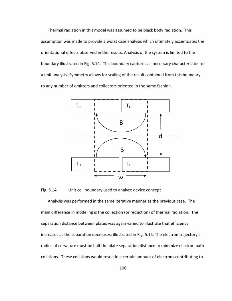
106
Thermal radiation in this model was assumed to be black body radiation. This
assumption was made to provide a worst case analysis which ultimately accentuates the
orientational effects observed in the results. Analysis of the system is limited to the
boundary illustrated in Fig. 5.14. This boundary captures all necessary characteristics for
a unit analysis. Symmetry allows for scaling of the results obtained from this boundary
to any number of emitters and collectors oriented in the same fashion.
Fig. 5.14 Unit cell boundary used to analyze device concept
Analysis was performed in the same iterative manner as the previous case. The
main difference in modeling is the collection (or reduction) of thermal radiation. The
separation distance between plates was again varied to illustrate that efficiency
increases as the separation decreases; illustrated in Fig. 5.15. The electron trajectory’s
radius of curvature must be half the plate separation distance to minimize electron path
collisions. These collisions would result in a certain amount of electrons contributing to
TH TC
TH TC
B
w
d
B

107
back emission. Back emission reduces the net current and thus reduces power and
efficiency.
Fig. 5.15 Device efficiency for varying plate separation. The emitter and collector temperatures are 1000 K and 300 K, respectively. The emitter and collector work functions are 2 eV and 1 eV, respectively.
The efficiency for varying emitter source temperatures is illustrated in Fig. 5.16 and is
calculated using equation 3.6 to estimate thermionic emission, equations 5.5 - 5.11 to
estimate heat transfer and equations 4.1 - 4.3 to calculate efficiencies. Interestingly the
efficiency profile is similar to that obtained in the 1st order modeling effort where the
only thermal losses where those due to radiation exchange between electrodes. An
obvious efficiency optimum is obtained for a certain emitter source temperature. The
Carnot efficiency is no longer violated because there is thermal communication via small
amounts of thermal radiation exchange between electrodes.

108
Fig. 5.16 Device efficiency and power density for varying emitter temperatures. The emitter and collector work functions are 2 eV and 1 eV, respectively.
The device efficiency for varying emitter work functions is illustrated in Fig. 5.17.
The collector work function is assumed to be 1 eV. The emitter and collector source
temperatures are held at 1000 K and 300 K, respectively. An optimum emitter work
function occurs due to an increase in emission current. As the work function is reduced
higher emission currents are realized, however at the same time the device voltage is
decreasing because the work function is decreasing. This is the primary reason for the
optimum efficiency. Operating at the optimum efficiency will not provide the highest
power density. As both Fig. 5.16 and Fig. 5.17 illustrate the maximum power densities
occur for the highest emitter operating temperatures and lower emitter work functions.
0
0.1
0.2
0.3
0.4
0.5
0.6
0.7
0.8
0.9
1
500 600 700 800 900 1000 1100 1200 1300 1400 1500
Emitter Temperature, Th [K]
Eff
icie
ncy
0
5
10
15
20
25
30
35
40
45
50
Po
wer
Den
sit
y [
W/c
m^
2]
1st Law
Carnot
2nd Law
Electrical Power [W]
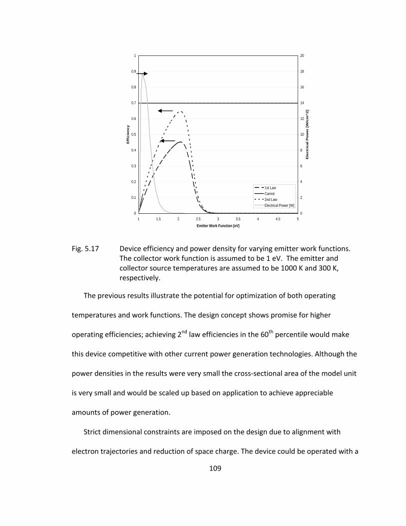
109
Fig. 5.17 Device efficiency and power density for varying emitter work functions. The collector work function is assumed to be 1 eV. The emitter and collector source temperatures are assumed to be 1000 K and 300 K, respectively.
The previous results illustrate the potential for optimization of both operating
temperatures and work functions. The design concept shows promise for higher
operating efficiencies; achieving 2nd law efficiencies in the 60th percentile would make
this device competitive with other current power generation technologies. Although the
power densities in the results were very small the cross-sectional area of the model unit
is very small and would be scaled up based on application to achieve appreciable
amounts of power generation.
Strict dimensional constraints are imposed on the design due to alignment with
electron trajectories and reduction of space charge. The device could be operated with a
0
0.1
0.2
0.3
0.4
0.5
0.6
0.7
0.8
0.9
1
1 1.5 2 2.5 3 3.5 4 4.5 5
Emitter Work Function [eV]
Eff
icie
nc
y
0
2
4
6
8
10
12
14
16
18
20
Ele
ctr
ical
Po
we
r [W
/cm
^2
]
1st Law
Carnot
2nd Law
Electrical Power [W]

110
magnetic field similar to that of a strong laboratory magnet. The electron trajectory’s
radius of curvature would be roughly 0.5 microns which will result in a plate width and
separation distance of 1 micron. The space charge is not significant for these dimensions
due to the low current density. These device dimensions are within the fabrication
limits of the current state of the art.
Alternating hot and cold plates would require a design that isolates the hot from
cold plates. Spreader technology such as heat pipes, vapor chambers, and
microchannels could provide the link between the source and hot plates as well as the
link between the cold plates and collector heat sink.
iii. TFE NANOWIRE CONVERTOR
Small scale dimensions are also an attribute of the second device investigated in this
work; which has been named the TFE Nanowire Converter. TFE has been shown to have
distinct advantages over TI emission. Specifically the addition of the electric field
reduces the required operating temperature and work function to achieve appreciable
current densities. One of the challenges in implementing TFE is achieving a sufficient
electric field to enhance emission. Many studies have shown that the use of the strong
electric field around a sharp point can provide a suitable field at relatively low applied
voltages.
A stronger electric field can be generated around a very small radii point source.
The point sources can be arranged in an array to achieve maximum power densities. For
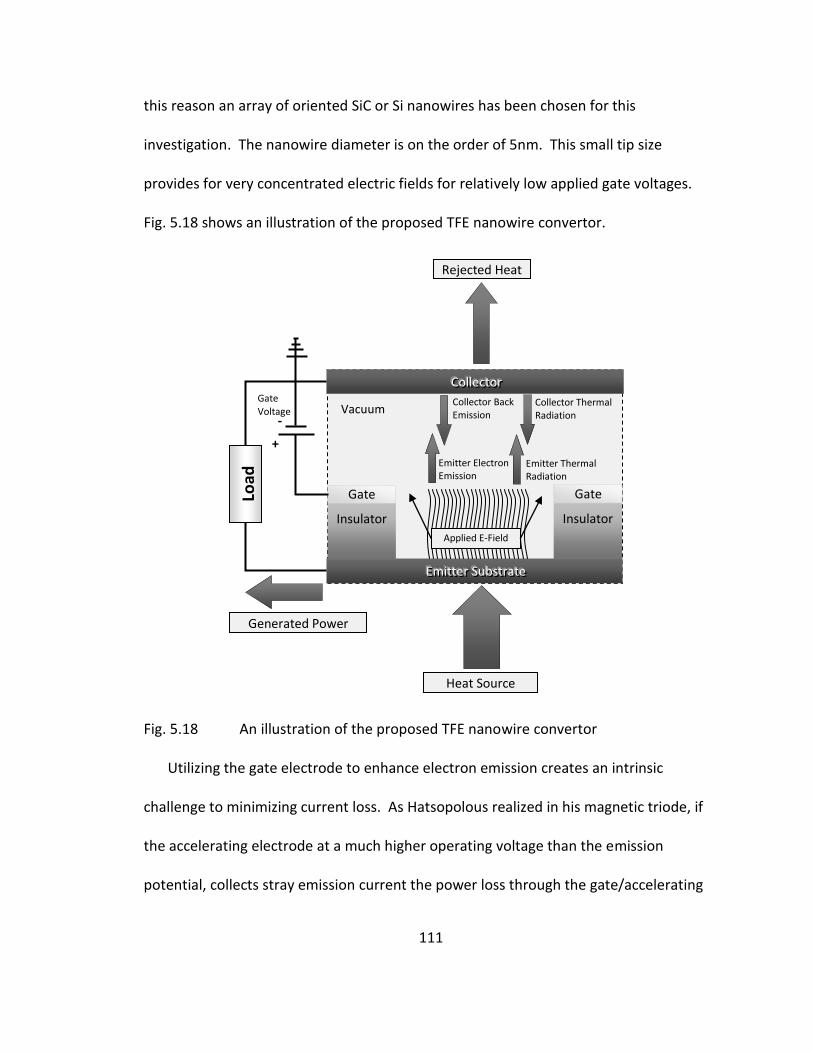
111
this reason an array of oriented SiC or Si nanowires has been chosen for this
investigation. The nanowire diameter is on the order of 5nm. This small tip size
provides for very concentrated electric fields for relatively low applied gate voltages.
Fig. 5.18 shows an illustration of the proposed TFE nanowire convertor.
Fig. 5.18 An illustration of the proposed TFE nanowire convertor
Utilizing the gate electrode to enhance electron emission creates an intrinsic
challenge to minimizing current loss. As Hatsopolous realized in his magnetic triode, if
the accelerating electrode at a much higher operating voltage than the emission
potential, collects stray emission current the power loss through the gate/accelerating
EEEmmmiiitttttteeerrr SSSuuubbbssstttrrraaattteee
Gate
CCCooolll llleeeccctttooorrr
Load
Insulator
Gate
+
-
Insulator
Emitter Electron Emission
Collector Back Emission
Emitter Thermal Radiation
Collector Thermal Radiation
Rejected Heat
Applied E-Field
Gate Voltage
Heat Source
Generated Power
Vacuum
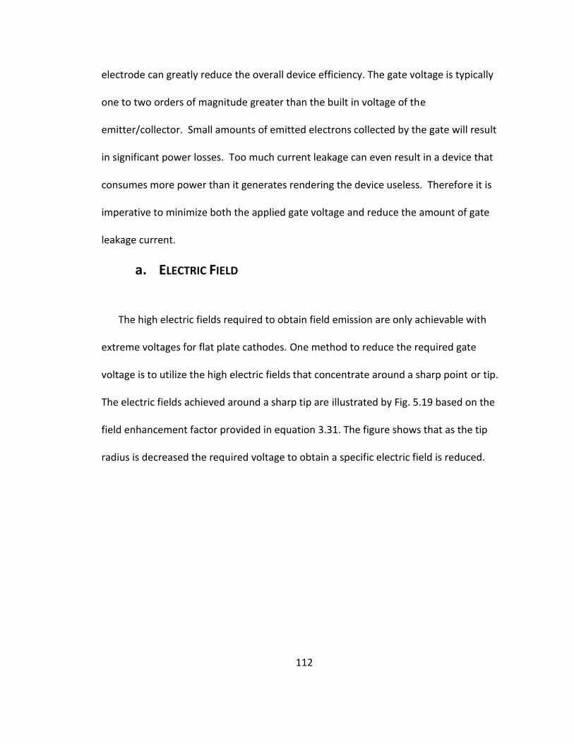
112
electrode can greatly reduce the overall device efficiency. The gate voltage is typically
one to two orders of magnitude greater than the built in voltage of the
emitter/collector. Small amounts of emitted electrons collected by the gate will result
in significant power losses. Too much current leakage can even result in a device that
consumes more power than it generates rendering the device useless. Therefore it is
imperative to minimize both the applied gate voltage and reduce the amount of gate
leakage current.
a. ELECTRIC FIELD
The high electric fields required to obtain field emission are only achievable with
extreme voltages for flat plate cathodes. One method to reduce the required gate
voltage is to utilize the high electric fields that concentrate around a sharp point or tip.
The electric fields achieved around a sharp tip are illustrated by Fig. 5.19 based on the
field enhancement factor provided in equation 3.31. The figure shows that as the tip
radius is decreased the required voltage to obtain a specific electric field is reduced.

113
Fig. 5.19 Electric field strength for various tip radii and operating voltages
b. TIP EMISSION & FIELD EMITTER ARRAYS
Tip emission has been thoroughly investigated for use as field emission cathodes.
Carbon nanotube field emission has been demonstrated by (Zhu, et al. 1999). Nanowire
field emission has been illustrated by (Liu, et al. 2005) (Z. Pan, et al. 2000).
The plot in Fig. 5.20 was developed using the simplified TFE model for a potential
barrier between parallel plates (equations 3.36 through 3.45) for 3C silicon carbide (SiC)
with a work function of 4.4 eV (Wu, et al. 2002). Emission was estimated based on a
projected emitter area as opposed to the profile area of the nanowires. The chart
0
50
100
150
200
250
0 5 10 15 20
Vo
ltag
e [
V]
Tip Radius [nm]
2E3 V/micron
4E3 V/micron
6E3 V/micron
8E3 V/micron
1E4 V/micron
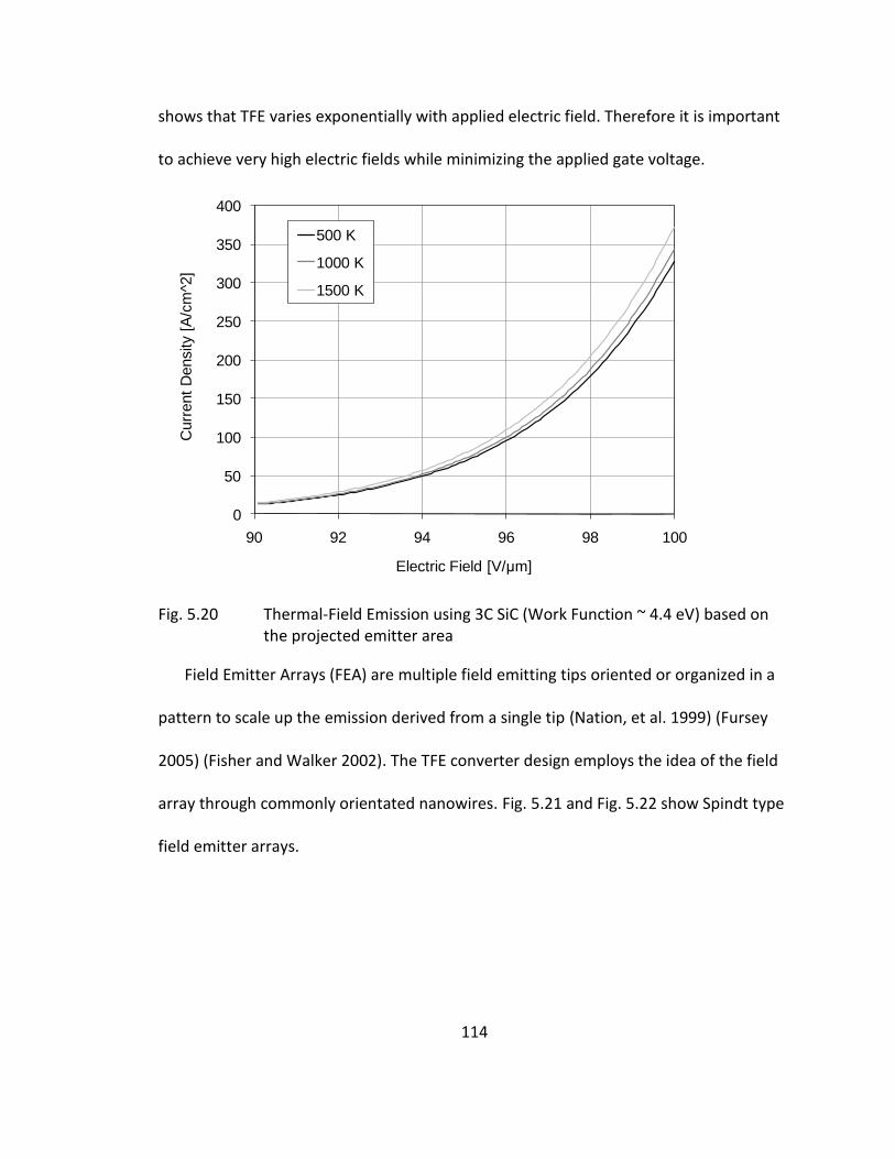
114
shows that TFE varies exponentially with applied electric field. Therefore it is important
to achieve very high electric fields while minimizing the applied gate voltage.
Fig. 5.20 Thermal-Field Emission using 3C SiC (Work Function ~ 4.4 eV) based on the projected emitter area
Field Emitter Arrays (FEA) are multiple field emitting tips oriented or organized in a
pattern to scale up the emission derived from a single tip (Nation, et al. 1999) (Fursey
2005) (Fisher and Walker 2002). The TFE converter design employs the idea of the field
array through commonly orientated nanowires. Fig. 5.21 and Fig. 5.22 show Spindt type
field emitter arrays.
0
50
100
150
200
250
300
350
400
90 92 94 96 98 100
Curr
ent
Density [
A/c
m^2
]
Electric Field [V/μm]
500 K
1000 K
1500 K

115
Fig. 5.21 Illustration gated field emitter array (Nation, et al. 1999)
Fig. 5.22 SEM of gated field emitter array (Nation, et al. 1999)
The Spindt type field emitter arrays are similar to proposed nanowire field
emitter array except that the pyramid tip emitters are replaced by oriented nanowires.
Nanowires offer larger aspect ratios which improve the field enhancement factor and

116
nanowires can be grown in greater densities than pyramids tip emitters. The larger
aspect ratios offer better field enhancement and Fig. 5.23 shows the experimental
setup used to evaluate field emission properties of SiC nanowires in a study performed
by (Z. Pan, et al. n.d.).
Fig. 5.23 Illustration of the experimental setup used to evaluate SiC nanowire field emission (Z. Pan, et al. n.d.)
Table 5.2 shows measured cold cathode emission currents from various tip
emission FEAs. The applied electric fields in these cases are much lower than those
suggested for TFE which occurs more readily at electric fields of around 1000 V/μm or
107 V/cm (Dolan & Dyke, 1954)(Fursey, 2005)(Murphy & Good Jr., 1956). The emission

117
models used in this thesis predict negligible emission currents at the electric fields levels
in these studies. This suggests that the emission modeling and assumptions in this
thesis are fairly conservative. The discrepancy between the modeling and experimental
results may be due to a number of factors. The studies don’t report an emitter work
function so the modeling was performed with assumed values for the work function
based on the material. Also, the studies don’t indicate whether the current density is
based on a projected emitter area or the actual profile area of the 3-D emitter surface.
Table 5.2 Tabulated empirical results for arrays of field emitters with nanoscale tip emitters (Nation, et al., 1999)(Pan, et al., 2000)(Teo, et al., 2002)
c. SERVER WASTE HEAT APPLICATION
The TFE convertor design is not limited to a specific heat source application, but can
be optimized per application. In the following example the TFE convertor is used to
scavenge server component waste heat. Modeling was performed for a 150 W
component with an operating temperature limit of 400 K. The collector and shunt heat
sinks, as shown in Fig. 5.24, are assumed to dissipate their heat into a 300 K ambient.
The shunt heat sink thermal resistance was sized such that the operating temperature is
maintained at a constant 400 K. A constant component temperature can be achieved
Study Nation et al Pan et al Teo et al
Emitter Description Si FEA Pyramids Oriented SiC Nanowires Carbon Nanofibers
Tip Radius [nm] 5 10-40 5
Electric Field [V/μm] Not Reported 2.5-3.5 7
Tip Density [per cm2] 3 x10⁶ 109-1010 106-109
Current Density [A/cm2] 2.1 1.0 x10⁻² 1.0 x10⁻³

118
with closed-loop feedback control between the component temperature and the air
mover.
Fig. 5.24 Proposed server implementation the TFE convertor
The generator area should be maximized to increase the amount of converted waste
heat. The area is assumed to be 200 cm2 based on the footprint for a large
microprocessor heat sink. However the power is normalized over the area to better
understand the generator performance independent of implemented area.
Using the TFE model provided in equations 3.30 and 3.36 through 3.45 and the
energy balances in equations 4.9 - 4.10, a parametric study of component temperature
and gate voltage effect on the generated power density was performed and shown in
TFE Generator
Component (Heat Source)
Heat Spreader
Shunt Heat Sink
Collector Heat Sink
TS
ψSpreader
TE
TC
ψHeat Sink
ψShunt Heat Sink
T∞
TFE Generator

119
Fig. 5.25 and Fig. 5.26. The plots show that there is a stronger dependence on applied
gate voltage than component operating temperature. Fig. 5.26, also shows that better
generation can be achieved at lower tip radii. From a device feasibility perspective the
power density results from this model are promising and would mean in significant
power savings in current server hardware.
Fig. 5.25 TFE generated power density for a range of applied gate voltages (11.5V -13.0 V) and component temperatures with a 10nm tip radius, 3 eV emitter work function, 1.6 eV collector work function, and ambient temperature of 300 K
0.0
0.2
0.4
0.6
0.8
1.0
300 350 400 450 500
Ge
ne
rate
d P
ow
er
De
nsi
ty
[W/
cm^
2]
Temperature [K]
11.5V
12.0V
12.5V
13.0V

120
Fig. 5.26 TFE generated power density from a 150 W device for a range on nanowire radii (5 nm – 15 nm) and applied gate voltages with a 400 K component temperature, 300 K ambient temperature, 3 eV emitter work function, and 1.6 eV collector work function
Based on the current the electrical load should be sized such that the voltage is
equal to the difference in work function. The operating potential can only be as high as
the difference in work function. If the load is too high then the current will be
restricted. Conversely, if the load is too low then the voltage will be less than the
potential difference in electrodes and result in a reduction in power generation. Fig.
5.27 (A) illustrates that there is an optimal load resistance to maximize power
generation and as expected the optimum efficiency of the device occurs at the optimum
load resistance as shown in Fig. 5.27 (B).
0.0
0.2
0.4
0.6
0.8
1.0
0.0 5.0 10.0 15.0 20.0
Ge
ne
rate
d P
ow
er
De
nsi
ty
[W/
cm^
2]
Gate Voltage [V]
5 nm
10 nm
15 nm

121
Fig. 5.27 Plot of (a) power density, current density, operating voltage, and (b) efficiencies as function of load resistance
0.0
0.2
0.4
0.6
0.8
1.0
1.2
1.4
1.6
0.0
0.1
0.2
0.3
0.4
0.5
0.6
0.00 0.05 0.10 0.15
Op
era
tin
g V
olt
ag
e [V
]
Po
wer
an
d C
urr
ent
Den
sity
[W/c
m2
an
d A
/cm
2]
Load Resistance [Ohms]
Power Density
Current Density
Operating Voltage
Optimal Load
Resistance 0.02Ω
Maximum Operating
Voltage = (ϕE-ϕC)
0.0%
0.5%
1.0%
1.5%
2.0%
0 0.05 0.1 0.15
Eff
icie
ncy
Load Resistance [Ohms]
1st Law Efficiency
2nd Law Efficiency
(A)
(B)

122
6. PROPOSED FABRICATION OF NANOWIRE BASED STRUCTURE
In parallel to this study, Silicon nanowires have been fabricated by Jeff Scott as part
of his undergraduate honors project and Dr. Hao Li of the University of Missouri-
Columbia Mechanical Engineering department (Scott and Solbrekken n.d.). The
following fabrication process and resulting nanowires are the sole achievement of Jeff
Scott and Hao Li. This chapter provides documentation of their process and success in
growing Si nanowires as well as a proposal for an experimental apparatus to test TFE
nanowire device performance.
The nanowires were fabricated using the Vapor-Liquid-Solid (VLS) growth
mechanism (Law et al., 2004 and (Wang, et al. 2000)), in a hot-wall Chemical Vapor
Deposition (CVD) chamber as illustrated in Fig. 6.1. Creation of oriented nanowires
starts with the fabrication of a substrate. A (111) oriented silicon substrate is chosen to
help promote oriented nanowire growth. Patterned gold is used as nucleation cites for
nanowire growth. Layers of organized sub micron polystyrene spheres are spun on the
surface (Fig. 6.2) of the substrate to create a mask for the gold pattern deposition as
shown in Fig. 6.3. The number of layers of spheres alters the size and density of
patterned gold nucleation sites.

123
Fig. 6.1 Sketch of the theoretical Si nanowire that results from SiO vapor and VLS mechanism. Adapted from (Kolb, et al. 2004) by (Scott and Solbrekken n.d.)
The VLS process starts with the condensation of the vapor into liquid nucleating at a
metal catalyst particle. The liquid then cools to form a solid. One dimensional growth
occurs to form a nanowire or nanorod due to thermal conduction from the substrate
solidifying the liquid. Condensation continues at the tip which is still in the liquid phase.
Properly controlling this growth mechanism can yield nanowires and nanorods of
varying dimension, as shown in Fig. 6.4. The diameter of the nanowire is controlled by
changing the size of catalyst particle and length of the nanowire is controlled by altering
growth time. Other deposition parameters such as temperature and pressure are also
of importance.
<111>
direction
Si substrate
SiO vapor
Si c
ore
SiO
2 sh
ell
SiO
2 sh
ell
Liquid Au/Si
droplet
(supersaturated)

124
Fig. 6.2 SEM images of a single layer of polystyrene spheres (Scott and Solbrekken n.d.)
Fig. 6.3 SEM images of patterned gold film resulting from a single layer of polystyrene spheres (Scott and Solbrekken n.d.)

125
Fig. 6.4 SEM images of Si nanowire growth (gray lines), as well as a large number of SiO2 deposits (white dots) (Scott and Solbrekken n.d.)
CVD Si nanowires grown with VLS or VS mechanism usually have an intrinsic thin
SiO2 or graphite layer depending on experimental conditions. The SiO2 layers can be
easily etched off by Hydrogen Fluoride and the graphite layer can be burned off. In
addition, the Si nanowires can also be oxidized at elevated temperatures to form SiO2
layers. Therefore, Si nanowire diameter could be controlled by post-oxidization and
chemical etching.
The Vapor-Solid (VS) growth mechanism can also be used where phase change from
vapor directly into solid occurs. Nanowires can also be formed using carbon nanotubes
as both a precursor and template. The nanowires shown in Fig. 6.5 were fabricated
using this method in the lab of Co-PI Hao.

126
Fig. 6.5 Free standing SiC nanowires made from graphite particles and carbon nanotubes (Photos courtesy of Dr. Hao Li)
It is necessary to build an experimental prototype to validate the analytic models
developed for the TFE nanowire convertor. The proposed experimental apparatus is
shown in Fig. 6.6.
Fig. 6.6 Proposed experiment for TFE convertor prototype
Metal Gate Gate Oxide Doped SiC Substrate (Cathode/Emitter)
Metal (Anode/Collector) Rlo
ad
DVM
Vacuum
Input Heat
-
+
Calorimeter
Thermocouples (To measure input heat flux)
Heat Sink
Rejected Heat
Gap Width
Collector Junction Temperature
Emitter Junction Temperature
Δx
500 nm 5 nm

127
The envisioned device will have a separate anode and gate. The electric field for
field emission is generated between the nanowire tips and the gate. The gate is
electrically isolated from the substrate by an oxide material which can be patterned
using photolithography. The oxide layer can be grown and a metal layer will be
deposited to form the gate. Photoresist is intended to protect the region where
nanowires are to be located and be removed prior to nanowire growth. Nanowire
growth will be performed using the hot-wall CVD and the VLS growth mechanism
discussed earlier. Metal catalyst particles on the Si substrate surface are used to initiate
the growth and control the diameter of the nanowires.
Leakage current through the gate is a major concern due to the higher gate voltage.
The gate surface area will be substantially smaller than that of the collector to help
minimize those losses. One of the goals for the experimental measurements is to
understand the losses caused by leakage current and to develop ways for reducing
those parasitic losses. Gate geometry, orientation and structure can be altered to
understand their effect on leakage current.
The physical dimensions of the nanowires, the packing density of the nanowires, and
the proximity to the metal gate can be characterized by scanning the cathode assembly
using a scanning electron microsope. It is expected that the experiments will need to be
conducted within a vacuum environment, although initial experiments can be
attempted in an ambient pressure environment.

128
7. CONCLUSIONS AND FUTURE STUDIES
Although there is a significant environmental push to reduce energy consumption
via waste heat recovery it is important to look at the bigger picture. For significant
adoption of such technologies to occur I believe the energy saved by the device must be
greater than the amount consumed to produce the device. Unless this is true, the net
effect will be a drain on the environment.
Energy costs are rising due to both increased consumption and/or reduced supply.
Adoption of solid state waste heat recovery has been cost prohibitive, but there will be
an inflection point where the cost savings due to energy reductions outweighs the
device/implementation costs of solid state recovery. Reduced manufacturing costs and
increased device efficiencies will help drive this inflection.
The converter designs proposed in this thesis show promise of increasing energy
conversion efficiency for solid state convertors, but are a long way from high volume
manufacturing. The Magnetic Diode and TFE Convertor both combine known
technologies and methods in a novel way. The materials and manufacturing methods
are available today to develop both proposed devices. Further material development,
specifically with regards to a material’s work function, will only improve the predicted
results for these devices. Further design and optimization is required to minimize
efficiency losses, and develop and refine manufacturing methods.

129
This thesis has presented unique substance including the invention of new and
novel solid state energy conversion devices combined with the unique application of
system level modeling approach and the novel application of waste heat recovery from
a server. Some modeling assumptions and approximations where made to allow for
estimating device efficiencies. These estimates provided an understanding of device
feasibility. With a first order feasibility of these devices understood now there is an
opportunity to add more modeling detail with less risk of the work being wasted on an
infeasible device. However, the system level thermal modeling performed in this thesis
is more detailed and provides for significantly improved results over the standard
approach of modeling emission with constant temperature boundary conditions.
i. MAGNETIC DIODE
The idea for the Magnetic Diode device was conceived with the intention to reduce
the parasitic thermal radiation losses suffered in a traditional face to face TI diode.
Thermal modeling illustrates that plate orientation provides a means to reduce the net
thermal radiation transfer from the emitter electrode(s) to the collector electrode(s).
Radiation from the electrodes is recovered using a like temperature plate facing the
respective electrode. Use of the magnetic field to alter the trajectory of the electrons is
a proven technique allowing for the unusual plate orientations. The modeling
performed for the Magnetic Diode illustrates that a 2nd law efficiency of roughly 65%

130
could in theory be achieved. This is a marked improvement over many of the competing
devices (namely TE or conventional TI conversion).
The conclusion must be drawn that with existing material work functions at roughly
1.8 eV, low temperature operation (~1000 K) may be efficient but power densities will
be very low (~ 0.01 W/cm2). This device may achieve higher output power by increasing
the source temperature; however there is a minor loss in efficiency. This device
illustrates a unique way to minimize thermal radiation losses by careful orientation of
the electrodes. Enhanced efficiencies are theoretically possible, however low
temperature TI emission is impractical with current state of the art materials.
Despite all of the proven technologies employed in this device there are still
significant hurdles to overcome even for high temperature operation. The challenges
facing the Magnetic Diode that would serve as next steps include: validation of the
electron scattering effect, magnetic field design and application.
ii. TFE NANOWIRE CONVERTOR
Unlike TI emission, TFE can provide significant current densities at low temperatures.
The modeling shows that power densities on the order of 0.5 W/cm2 can theoretically
be achieved with this device with an applied voltage of 5-10V depending upon the
diameter of the nanowire radius. If this level of generation can be achieved in practice
then there would be opportunity to recover significant quantities of waste energy from
server components.

131
The next steps for the TFE nanowire convertor research would be to develop a more
accurate model as well as experimentation to fully understand the magnitude and
nature of leakage currents into the gate electrode. First steps in the fabrication of this
device have been taken. Silicon nanowires have been produced per the VLS method.
The next step in fabrication is to develop the ability to develop a method that
incorporates the gate structure with the oriented nanowires.

132
8. APPENDIX
i. GENERIC THERMIONIC MODEL
The following is an example of Matlab code used to iteratively solve a parametric
study of emitter temperature on device efficiency of a thermionic diode:
% Dominick Lovicott
% Thermionic Research
% Example Thermal Resistance Model
clear
clc
% Constants
KB = 1.381*10^-23; % Boltzmann's Constant[J/K]
Eo = 8.854*10^-12; % Permittivity of a Vacuum[F/m]
m = 9.109*10^-31; % Mass of an Electron[kg]
e = 1.602*10^-19; % Charge of an electron [C]
sigma = 5.67*10^-8; % Stefan-Boltzmann Constant[W/m^2*K^4]
pi = 3.14159265359;
A1 = 1200000; % Emission Constant[Amps/m^2]
% Temperature Variables
T8E = 1500; % Hot side Temperature[K]
T8Emin = 500; % Hot side minimum temperature[K]
T8C = 300; % Cold side Temperature[K]
% Misc
L = 1*10^-2; % Thickness of emitter and collector plates[m]
A = 1; % Crossectional area of emitter and collector plates[m^2]
KE = 150; % Thermal conductivity of emitter plate[W/mK]
KC = 150; % Thermal conductivity of collector plate[W/mK]
EWF= 3; % Emitter work function[eV]
CWF = 2; % Collector work function[eV]
RE = .02; % Thermal Resistance of emitter surface[K/W]
RC = .02; % Thermal Resistnace of collector surface[K/W]
EE = .5; % Emissivity of Emitter surface
EC = 1; % Emissivity of Collector surface
% View Factors
% Radiation view factor for the emission from the emitter as seen by
% the collector
fE = .5;
% Radiation view factor for the emission from the collector as seen by
% the emitter

133
fC = .5;
% Iteration Variables
O = 2; % Number of k loop iterations (effieciency dependance)
delta_k = (T8E-T8Emin)/O; % k loop scaling constant
tol = 10^-9; % tolerance of convergence
for k=1:O % Iteration loop for efficiency dependance
M = 100; % Number of i loop iterations
delta_i = 1/M; % i loop scaling constant
% Calculation of emitter side source temperature[K]
T8E = delta_k*k + T8Emin;
% tracking of the emitter source temperature for plotting[K]
T8Et(k) = delta_k*k + T8Emin;
for i=1:M % Iteration loop for temperature calculations
if i==1
TET = T8E-100; % Temperature at the top of the emitter plate[K]
TCT = T8C+100; % Temperature at the top of the collector plate[K]
TEB = T8E-100; % Initial temperature of the bottom of the emitter[K]
% Initial temperature of the bottom of the collector[K]
TCB = T8C+100;
else
iteration(i)= i-1;% Keeps track of iterations for plotting purposes
% Current density emitted by the emitter[Amps/m^2]
JE(k) = (A1*TET(i-1)^2)*exp(-e*EWF/(KB*TET(i-1)));
% Current density emitted by collector (AKA back emission)
% [Amps/m^2]
JC(k) = (A1*TCT(i-1)^2)*exp(-e*CWF/(KB*TCT(i-1)));
% Radiation emitted from the emitter[W]
qRE(i) = EE*A*sigma*TET(i-1)^4;
% Radiation emitted from the collector[W]
qRC(i) = EC*A*sigma*TCT(i-1)^4;
% Heat rejected from the emitter due to emission [W]
qE(i) = JE(k)*(EWF+(2*KB*TET(i-1)/e));
% Heat rejected from the collector due to emission[W]
qBE(i) = JC(k)*(EWF+(2*KB*TCT(i-1)/e))-(EWF-CWF)*(JE(k)-JC(k));
% Heat supplied to the emitter plate [W]
qs(k) = qRE(i)-fE*qRC(i)+qE(i)-qBE(i);
% Heat rejected by the collector plate[W]
qo(k) = fE*qRE(i)-qRC(i)+qE(i)-qBE(i);
% Temperature of the bottom of the emitter plate [K]
TEB(i) = -(qs(k))*RE+T8E;
% Temperature of the bottom of the collector plate[K]
TCB(i) = (qo(k))*RC+T8C;
% Temperature of the top of the emitter plate[K]
TET(i) = TEB(i)-qs(k)*(L/(KE*A));
% Temperature of the top of the collector plate [K]
TCT(i) = TCB(i)+qo(k)*(L/(KC*A));
% Difference in temperature for the top of the emitter between the

134
% previous and current iteration [K]
delta_TET = abs(TET(i) - TET(i-1));
% Difference in temperature for the top of the collector between
% the previous and current iteration [K]
delta_TCT = abs(TCT(i) - TCT(i-1));
if (delta_TET >= tol)
M=M+1;
elseif (delta_TCT >= tol)
M=M+1;
end
end
end
% Efficiencies
efficiency_1(k) = (EWF-CWF)*(JE(k)-JC(k))/(qs(k)); % 1st law efficiency
efficiency_C(k) = 1-(T8C/T8E); % Carnot efficiency
efficiency_2(k) = efficiency_1(k)/efficiency_C(k); % 2nd law efficiency
end
% Plots
figure(1)
plot(iteration,TET,iteration,TEB,':')
title('Emitter Plate Temperatures')
xlabel('Iteration')
ylabel('Temperature [K]')
figure(2)
plot(iteration,TCT,iteration,TCB,':')
title('Collector Plate Temperature')
xlabel('Iteration')
ylabel('Temperature [K]')
figure(3)
plot(T8Et,efficiency_1,T8Et,efficiency_2,':')
title('Efficiency vs Temperature')
xlabel('Temperature [K]')
ylabel('Efficiency')
ii. MAGNETIC DIODE MODEL
The following is an example of the Matlab code used to estimate Thermionic
emission current and efficiency as a function of temperature for various plate
separation angles of the Magnetic Diode:

135
% Constants
KB = 1.381*10^-23; % Boltzmann's constant e = 1.602*10^-19; % charge of an electron sigma = 5.67*10^-8; % Stefan-Boltzmann Constant pi = 3.14159265359; A1 = 120; % Thermionic emission constant
% Variables
Ee = 1; % emitter emissivity Ec = 1; % collector emissivity
Te_max = 2000; % Max Emitter temperature Te_min = 400; % Min Emitter temperature Tc = 273+100; % Collector temperature EWF = 3; % Emitter Work Function CWF = 1; % Collector Work Function a_max = pi; % Maximum angle of plate separation
Na = 5; % Number of iterations for plate separtion angle NT = 100; % Number of iterations for temperature
deltaa = a_max/Na; % Iteration size for separation angle deltaT = (Te_max-Te_min)/NT; % Iteration size for temperature
for i=1:Na % Separation angle of 0
if (i==1) a(i)=0; JC(i) =A1*Tc^2*exp(-e*CWF/(KB*Tc));
elseif (i==2) % Separation angle of Pi/2 a(i)=pi/2; JC(i) = 0; elseif (i==3) % Separation angle of Pi/1.1 a(i) = pi/1.1; JC(i) = 0; elseif (i==4) % Separation angle of Pi/4 a(i) = pi/1.01; JC(i) = 0; elseif (i==5) % Separation angle of Pi a(i) = pi; JC(i) = 0; end
a_d(i) = a(i)*180/(pi);
for j=1:NT % iteration loop for emitter temperature

136
Te(i,j) = deltaT*j+Te_min; % Emitter temperature calculation
%Emitter current JE(i,j) = A1*Te(i,j)^2*exp(-e*EWF/(KB*Te(i,j)));
% Thermal Radiation exchange Qr(i,j) = (1-sin(a(i)/2))*Ai*sigma*(Te(i,j)^4-Tc^4)/(1/Ee+1/Ec-
1);
% 1st law efficiency NI(i,j) = ((JE(i,j)-JC(i))*(EWF-CWF))/ (Qr(i,j)+JE(i,j)*(EWF+(2*KB*Te(i,j))/e)-JC(i)*(EWF+2*KB*Tc/e));
% Carnot Efficiency NC(i,j) = 1 - (Tc/Te(i,j));
% 2nd Law Efficiency NII(i,j) = NI(i,j)/NC(i,j); end
end
figure(1) plot(Te,NI(1,:),'-',Te,NI(2,:),'--',Te,NI(3,:),':',Te,NI(4,:),':', Te,NI(5,:),':',Te,NC(1,:)) xlabel('Temperature, [K]') ylabel('Efficiency')

137
REFERENCES
Angrist, S. W. (1976). Direct Energy Conversion. Boston, MA.
Bejan, A. (1997). Advanced Engineering Thermodynamics (Second Edition ed.). New York.
Belady, C. L. (2007). In the data center, power and cooling costs more than the IT equipment it supports. Retrieved February 3, 2008, from http://electronics-cooling.com/articles/2007/feb/a3/
Brodie, I., & Schwoebel, P. R. (1994). Vacuum Microelectronic Devices. Proceedings of the IEEE , 1007-1034.
Caswell, W. (2007, January). DELL H2C TECHNOLOGY:HYBRID COOLING FOR OVERCLOCKED CPUS. Retrieved Februaury 20, 2010, from www.dell.com: http://www.dell.com/downloads/global/vectors/h2c.pdf
Cengel, Y. A., & Boles, M. A. (2002). Thermodynamics: An Engineering Approach. New York: McGraw-Hill.
Child, C. D. (1911). Discharge from Hot Cao. Physical Review , 32, 492-511.
CRC Press, Inc. (1983-1984). CRC Handbook of Chemistry and Physics: 64th Edition. Boca Raton: CRC Press, Inc.
Dolan, W. W., & Dyke, W. P. (1954). Temperature-and-Field Emission of Electrons form Metals. Physical Review , 95, 339-348.
Dushman, S. (1923). Electron Emission from Metals as a Function of Temperature. Physical Review , 21 (6), 623-636.
Energy Information Administration. (2006). Annual Energy Review. DOE.
Energy Information Administration. (2007). International Energy Outlook. U.S. Department of Energy.
ENERGY STAR program. (2007). Report to Congress on Server and Data Center Energy Efficiency. U.S Environmental Protection Agency.
EPA Office of Air and Radiation. (2003). ENERGY STAR: The Power to Protect the Environment Through Energy Efficiency. US EPA.
EPA. (2007). Report to Congress on Server and Datacenter Energy Efficiency.

138
Fairbanks, J. W. (2006). Thermoelectric Developments for Vehicular Applications. Diesel Engine-Efficiency and Emissions Research (DEER) Conference, (p. 81). Detroit, MI.
Fisher, T. S., & Walker, D. G. (2002). Thermal and Electrical Energy Transport and Conversion in Nanoscale Electron Field Emission Processes. Journal of Heat Transfer , 124 (5), 944-961.
Fowler, R. H., & Nordheim, L. (1928). Electron Emission in Intense Electric Fields. Proceedings of the Royal Society of London , Series A, 173-181.
Fursey, G. (2005). Field Emission in Vacuum Microelectronics. New York: Kluwer Academic/Plenum Publishers.
Gaertner, G., Geittner, P., Lydtin, H., & Ritz, A. (1997). Emission properties of top-layer scandate cathodes prepared by LAD. Applied Surface Science , 11-17.
Guth, E., & Mullin, C. J. (1942). Electron Emission of Metals in Electric Fields. Physical Review , 61, 339-348.
Hatsopolous, G. N. (1956, May). The Thermo-Electron Engine. Thesis .
Hatsopoulos, G. N., & Gyftopoulos, E. P. (1973). Thermionic Energy Conversion: Volume I: Processes and Devices. Cambridge, MA.
Hishinuma, Y., Geballe, T. H., & Moyzhes, B. Y. (2001). Refrigeration by combined tenneling and thermionic emission in vacuum: Use of nanometer scale design. Applied Physics Letters , 2572-2574.
Inropera, F. P., & Dewitt, D. P. (2002). Introduction to Heat Transfer. New York: John Wiley & Sons.
Jensen, K. L., O'Shea, P. G., & Feldman, D. W. (2002). Generalized electron emission model for field, thermal, and photoemission. Applied Physics Letters , 20 (81), 3867-3869.
Kolb, F. M., Hofmeister, H., Scholz, M., Zacharias, M., Gosele, U., Ma, D. D., et al. (2004). Analysis of silicon nanowure growth by combining SiO evaporation with the VLS mechanism. J. Electroncem. Soc. (151), G472-G475.
Langmuir, I. (1923). The Effect of Space Charge and Initial Velocities on the Potential Distribution and Thermionic Current Between Parallel Plane Electrodes. Physical Review , 21 (4), 419-435.
Langmuir, I. (1913). The Effect of Space Charge and Residual Gases on Thermionic Currents in High Vacuum. Physical Review , 2 (6), 450-486.
139
Langmuir, I. (1929). The Interaction of Electron and Positive Ion Space Charges in Cathode Sheaths. Physical Review , 33 (6), 954-989.
Liu, B. D., Bando, Y., Tang, C. C., Xu, F. F., & Golberg, D. (2005). Exellent Field-Emission Properties of P-Doped GaN Nanowires. J. Phys. Chem. B , 21521-21524.
Mackie, W. A., Hinricks, C. H., & Davis, P. R. (1990). Effective Work Function Measurements of Advanced Cathode Materials via a Thermionic Projection Micrscope System. IEEE Transactions on Electron Devices , 37, 2568-2574.
Mahan, G. D., & Woods, L. M. (1998). Multilayer Thermionic Refrigeration. Physical Review Letters , 80 (18), 4016-4019.
Murphy, E. L., & Good Jr., R. H. (1956). Thermionic Emission, Field Emission, and the Transition Region. Physical Review , 102 (6), 1464-1474.
Nation, J. A., Schachter, L., Mako, F. M., Len, L. K., Peter, W., Tang, C., et al. (1999). Advances in Cold Cathode Physics and Technology. Proceedings of the IEEE , 87 (5), 865-889.
Office of Integrated Analysis and Forecasting. (1999). Federal Financial Interventions amd Subsides in Energy Markets 1999: Primary Energy. Washington DC: U.S. Department of Energy: Energy Information Administration.
Onsager, L. (1931). Reciprocal Relations in Irreversible Processes. I. Physical Review , 405-426.
Onsager, L. (1931). Reciprocal Relations in Irreversible Processes. II. Physical Review , 2265-2279.
Pan, Z., Lai, H.-L., Au, F. C., Duan, X., Zhou, W., Shi, W., et al. (2000). Oriented Silicon Carbide Nanowires: Synthesis and Field Emission Properties. Advanced Materials , 1186-1190.
Richardson, O. W. (1921). The Emission of Electricity form Hot Bodies (2nd Edition ed.). New York.
Scott, J., & Solbrekken, G. Fabrication of Vertically-Aligned Silicon Nanowires for use in Enhanced Emission Devices. MSGC Report.
Serway, R. A., & Beichner, R. J. (2000). Physics: For Scientists and Engineers. New York: Saunders College Publishing.
Shakouri, A., & Bowers, J. E. (1997). Heterostucture Integrated Thermionic Coolers. Applied Physics Letters , 1234-1236.

140
Solbrekken, G. L., Kazuaki, Y., & Bar-Cohen, A. (2004). Thermal Management of Portable Electronic Equipment using Thermoelectric Energy Conversion. IEEE Inter Society Conference on Thermal Phenomenon .
Solbrekken, G., Kazuaki, Y., & Bar-Cohen, A. (2004). Experimental Demonstration of Thermal Management using Thermoelectric Generation. IEEE Inter Society Conference on Thermal Phenomenon .
Soo, S. L. (1962). Analytical Thermodynamics. New Jersey: Prentice-Hall.
Tanner, P. G., Fraser, D. A., & Irving, A. D. (2005). Developments in thermionic engery converters. IEE Proc.-Sci Meas. Technol. , 152 (1).
Teo, K. B., Chhowalla, M., Amaratunga, G. A., Milne, W. I., Pirio, G., Legagneux, P., et al. (2002). Field emission from dense, sparse, and patterned arrays of carbon nanofibers. Applied Physics Letters , 2011-2013.
Tolman, R. C. (1920). The Entropy of Gases. J. Am. Chem. , 1185-1193.
Wang, Z. L., Dai, Z. R., Gao, R. P., Bai, Z. G., & Gole, J. L. (2000). Side-by-side Silicon Carbide - Silica Biaxial Nanowires: Synthesis, Structure, and Mechanical Properties. Applied Physics Letters , 3349-3351.
Waterman, A. T. (1924). The Variation of Thermionic Emission with Temperature and the Concentration of Free Electrons within Conductors. Physical Review , 24, 366-376.
Weisbart, R. A., & Coker, D. R. (2001, May 17). SEAT SURFACE TEMPERATURE IS THE LATEST MEASUREMENT OF CONSUMER COMFORT. Retrieved February 20, 2010, from www.amerigon.com: http://www.amerigon.com/pdfs/AUTOMOTIVE-INTERIORS-PAPER-5-15-01.pdf
Westover, T. L., & Fischer, T. S. (2006). Analysis and Simulation of Refrigeration by Electron Emission. IEEE , 1177-1184.
Westover, T. L., & Fisher, T. S. (2006). Analysis and Simulation of Refrigeration by Electron Emission. Thermal and Thermomechanical Phenomenon in Electronics Systems (pp. 1177-1184). Itherm.
Wu, Z. S., Deng, N. S., Chen, J., Zhou, J., & Chen, J. (2002). Needle-shaped silican carbide nanowires: Synthesis and field electron emission properties. Applied Physics Letters , 80 (20), 3829-3831.
Zhu, W., Bower, C., Zhou, O., Kochanski, G., & Jin, S. (1999). Large Current Density from Carbon Nanotube Field Emitters. Applied Physics Letters , 873-875.

141
Zuber, J. D., Jensen, K. L., & Sullivan, T. E. (2002). An analytical solution for mircotip field emission current and effective emission area. Journal of Applied Physics , 9379-9384.