Embed Size (px)
DESCRIPTION
MPhys thesis
Citation preview
UNIVERSITY OF EXETER
Transport Properties of Graphene
Doped with Adatoms
by
James McMurray
Collaborators: Chris Beckerleg and Will Smith
Supervisor: Dr. A. Shytov
April 2013

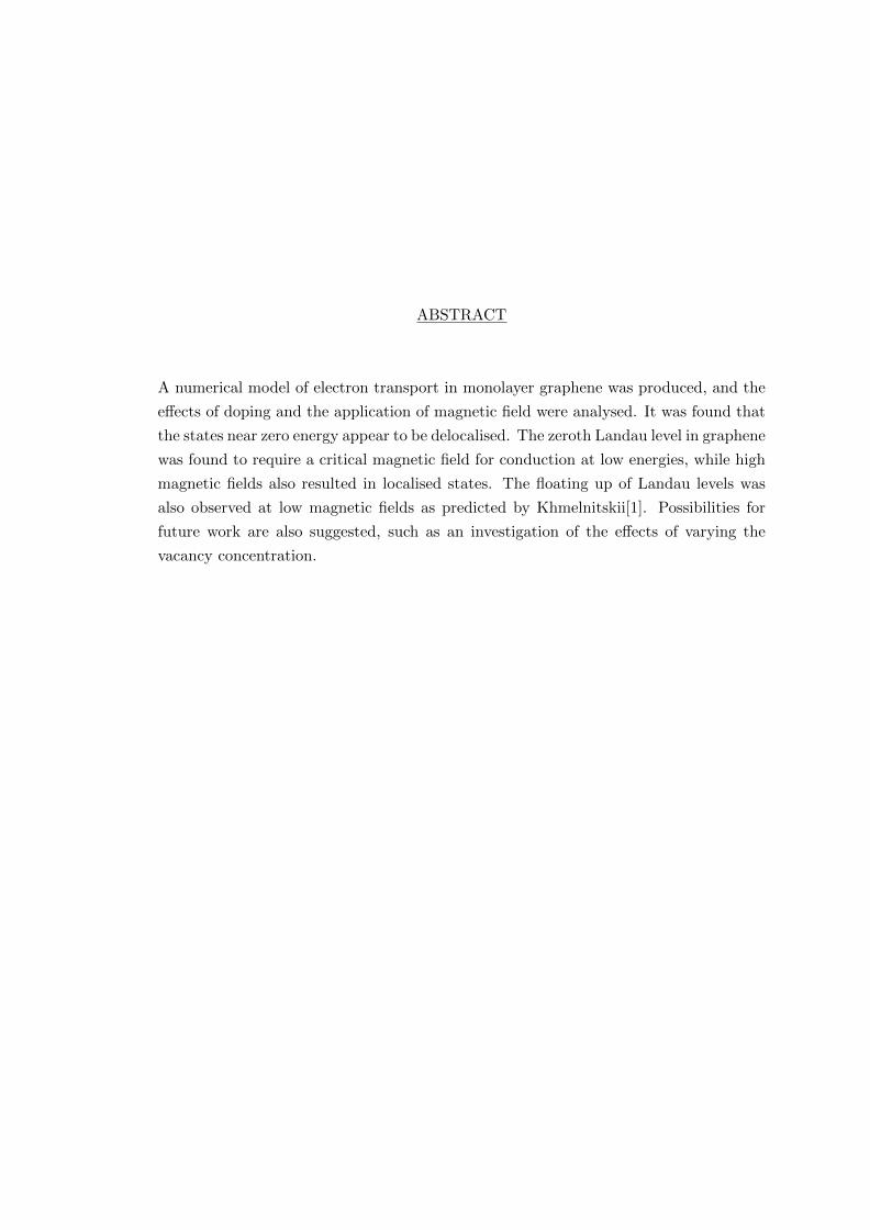
ABSTRACT
A numerical model of electron transport in monolayer graphene was produced, and the
effects of doping and the application of magnetic field were analysed. It was found that
the states near zero energy appear to be delocalised. The zeroth Landau level in graphene
was found to require a critical magnetic field for conduction at low energies, while high
magnetic fields also resulted in localised states. The floating up of Landau levels was
also observed at low magnetic fields as predicted by Khmelnitskii[1]. Possibilities for
future work are also suggested, such as an investigation of the effects of varying the
vacancy concentration.

Contents
1 Introduction 1
2 Background Theory 3
2.1 The lattice structure of graphene . . . . . . . . . . . . . . . . . . . . . . . 3
2.2 The Tight Binding approximation . . . . . . . . . . . . . . . . . . . . . . 4
2.3 Dirac points and the linear dispersion relation . . . . . . . . . . . . . . . . 5
2.4 Density of states . . . . . . . . . . . . . . . . . . . . . . . . . . . . . . . . 8
2.5 The Klein Effect . . . . . . . . . . . . . . . . . . . . . . . . . . . . . . . . 9
2.6 The Landauer Formula . . . . . . . . . . . . . . . . . . . . . . . . . . . . . 11
2.7 The Quantum Hall Effect . . . . . . . . . . . . . . . . . . . . . . . . . . . 11
2.8 Localisation . . . . . . . . . . . . . . . . . . . . . . . . . . . . . . . . . . . 13
3 Method and Implementation 15
3.1 Representation of the graphene sample . . . . . . . . . . . . . . . . . . . . 15
3.2 Scattering Matrix approach overview . . . . . . . . . . . . . . . . . . . . . 16
3.2.1 Generation of M matrix . . . . . . . . . . . . . . . . . . . . . . . . 17
3.2.2 Updating transmission matrices . . . . . . . . . . . . . . . . . . . . 18
3.3 Tests of correctness . . . . . . . . . . . . . . . . . . . . . . . . . . . . . . . 19
3.3.1 Unitarity checking . . . . . . . . . . . . . . . . . . . . . . . . . . . 19
3.3.2 Analytical tests . . . . . . . . . . . . . . . . . . . . . . . . . . . . . 20
3.4 Implementation of magnetic field . . . . . . . . . . . . . . . . . . . . . . . 23
3.5 Implementation of disorder . . . . . . . . . . . . . . . . . . . . . . . . . . 25
4 Results 27
4.1 Size effects . . . . . . . . . . . . . . . . . . . . . . . . . . . . . . . . . . . 28
4.2 Zero energy conductance peak . . . . . . . . . . . . . . . . . . . . . . . . . 29
4.3 Localisation length . . . . . . . . . . . . . . . . . . . . . . . . . . . . . . . 30
4.4 Phase diagrams . . . . . . . . . . . . . . . . . . . . . . . . . . . . . . . . . 31
4.5 Comparison with current experimental capabilities . . . . . . . . . . . . . 32
5 Conclusion 35
5.1 Summary . . . . . . . . . . . . . . . . . . . . . . . . . . . . . . . . . . . . 35
5.2 Future work . . . . . . . . . . . . . . . . . . . . . . . . . . . . . . . . . . . 35
A Flowchart 37
B Source code excerpts 39
B.1 Analytical ladder test program . . . . . . . . . . . . . . . . . . . . . . . . 39
v

vi CONTENTS
B.2 Allocation of random vacancy sites . . . . . . . . . . . . . . . . . . . . . . 40
Bibliography 43
List of Figures
2.1 A diagram of the real space lattice of graphene. Note the two sublatticesA and B. . . . . . . . . . . . . . . . . . . . . . . . . . . . . . . . . . . . . 3
2.2 Labelling the sites 1-4. . . . . . . . . . . . . . . . . . . . . . . . . . . . . . 4
2.3 A diagram of the band structure of graphene. The Dirac points are wherethe bands converge (zoomed on the right). Adapted from [11]. . . . . . . 6
2.4 A diagram of the first Brillouin zone in reciprocal space. The uniqueDirac points are K and K ′, M is the midpoint and Γ is the symmetrypoint shown as convention. . . . . . . . . . . . . . . . . . . . . . . . . . . 6
2.5 A plot of the density of states for a 50×86 sample with 3% vacancyconcentration on the A and B sublattices and 50 randomisations. . . . . 9
2.6 A plot of the transmission probability, T , as a function of the angle ofincidence, φ, for a potential of 285 meV (solid line) and 200meV (dashedline). Adapted from [5]. . . . . . . . . . . . . . . . . . . . . . . . . . . . . 10
2.7 A diagram showing the principle of how the transmission occurs across apotential barrier of height V, by shifting the electron to the lower cone.The filled area represents the portion filled with electrons. Note the con-stant Fermi level in the conduction band outside the barrier, and in thevalence band within it. Adapted from [5]. . . . . . . . . . . . . . . . . . . 10
2.8 A theoretical graph of the Hall conductivity (right axis, plateaus line)and longitudinal resistivity (left axis, peaks line) in monolayer graphene.Note the half-integer values of the Hall-conductivity and the peaks of thelongitudinal resistivity at the plateau steps. Adapted from [19]. . . . . . . 13
3.1 A diagram showing how the original graphene lattice structure is consid-ered as a “brick-wall” to simplify the links between lattice points. Thedashed lines separate the slices across which the transmission matricesare calculated and updated consecutively (this diagram shows the casefor conduction in the X direction). . . . . . . . . . . . . . . . . . . . . . . 16
3.2 A diagram of an example lattice to how the simultaneous equations areconstructed, in this case demonstrating the case of X-directed current.The different groups of sites are marked in different colours. . . . . . . . . 17
3.3 A diagram showing the net transmission across two blocks. One mustinclude the contributions from all of the possible paths, resulting in ageometric sum. . . . . . . . . . . . . . . . . . . . . . . . . . . . . . . . . . 19
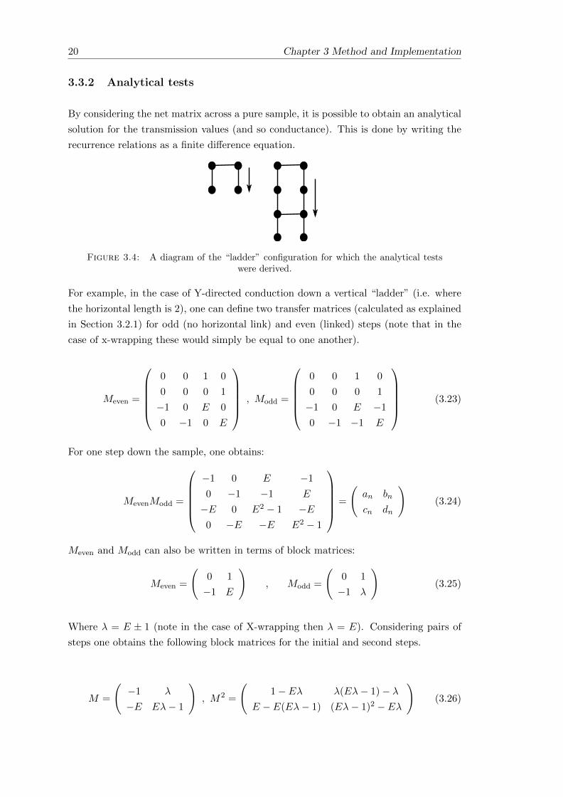
3.4 A diagram of the “ladder” configuration for which the analytical testswere derived. . . . . . . . . . . . . . . . . . . . . . . . . . . . . . . . . . . 20
vii
viii LIST OF FIGURES
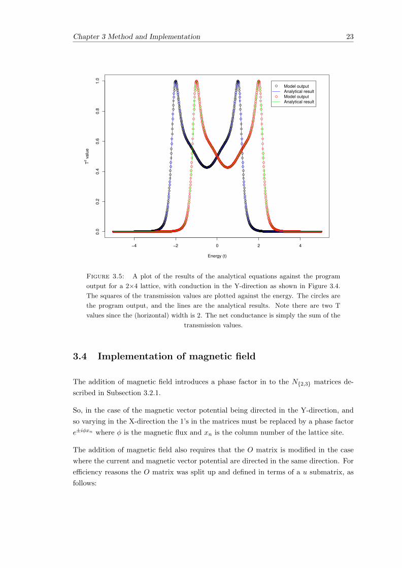
3.5 A plot of the results of the analytical equations against the programoutput for a 2×4 lattice, with conduction in the Y-direction as shown inFigure 3.4. The squares of the transmission values are plotted againstthe energy. The circles are the program output, and the lines are theanalytical results. Note there are two T values since the (horizontal)width is 2. The net conductance is simply the sum of the transmissionvalues. . . . . . . . . . . . . . . . . . . . . . . . . . . . . . . . . . . . . . 23
3.6 A plot of the quantum Hall steps in the wrapped and unwrapped con-ductance for a 160×277 sample, with the current in the X-direction andmagnetic vector potential in the Y-direction, at a flux of 0.0227. Thewrapped conductance is appropriately modified so it can be viewed onthe same scale. The theoretical values of the QHE steps are shown withdotted lines. . . . . . . . . . . . . . . . . . . . . . . . . . . . . . . . . . . . 25
4.1 Conductance for various sizes of square samples, showing the transitionfrom the delocalised to the localised regime near E = ± 0.2 . . . . . . . . 28
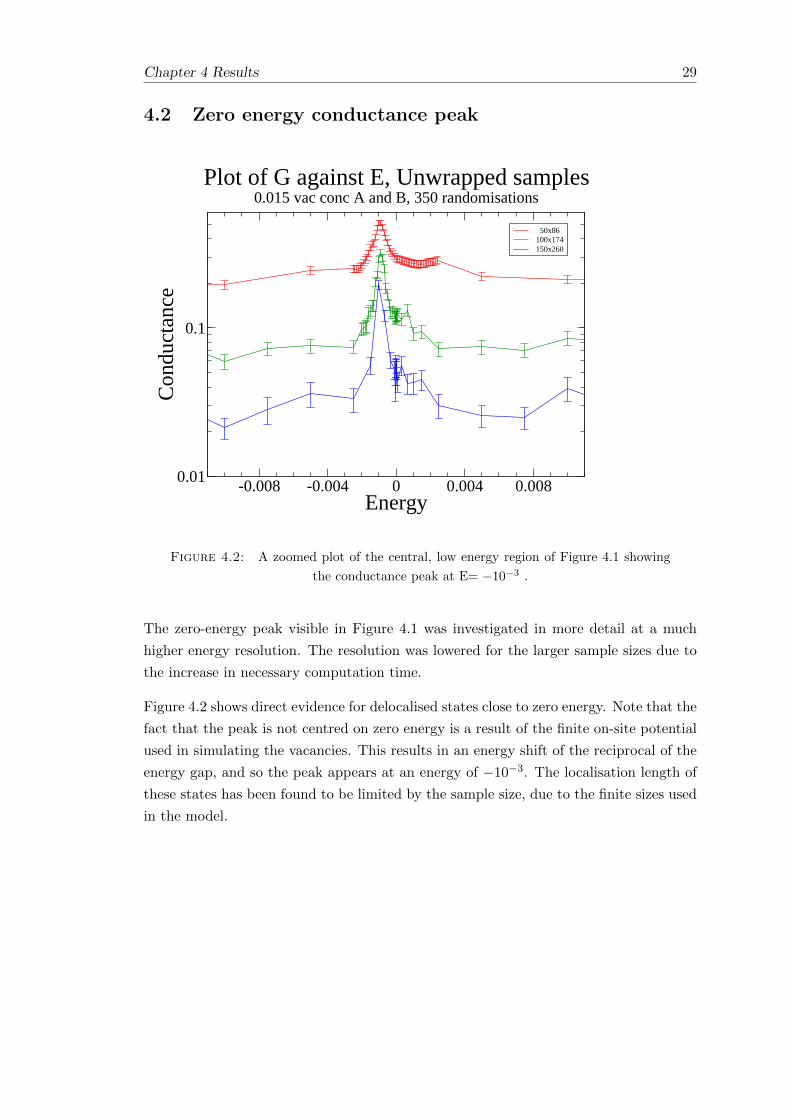
4.2 A zoomed plot of the central, low energy region of Figure 4.1 showing theconductance peak at E= −10−3 . . . . . . . . . . . . . . . . . . . . . . . 29
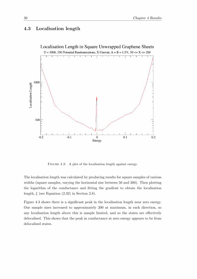
4.3 A plot of the localisation length against energy. . . . . . . . . . . . . . . . 30
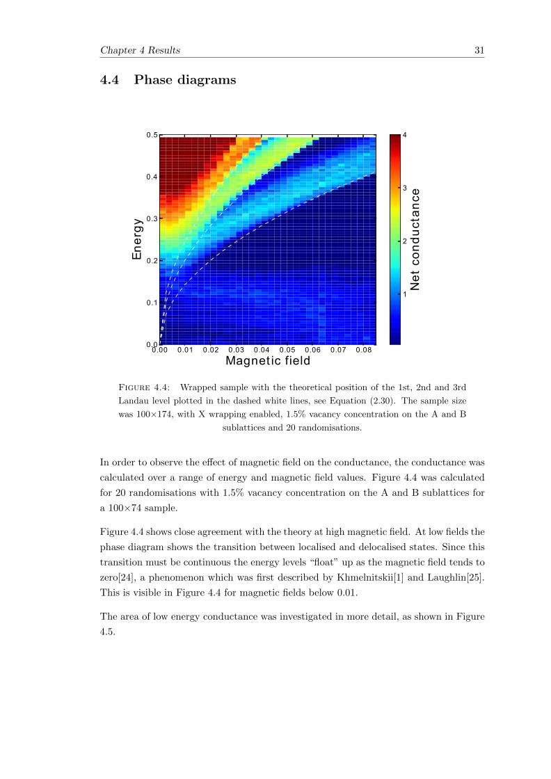
4.4 Wrapped sample with the theoretical position of the 1st, 2nd and 3rdLandau level plotted in the dashed white lines, see Equation (2.30). Thesample size was 100×174, with X wrapping enabled, 1.5% vacancy con-centration on the A and B sublattices and 20 randomisations. . . . . . . . 31
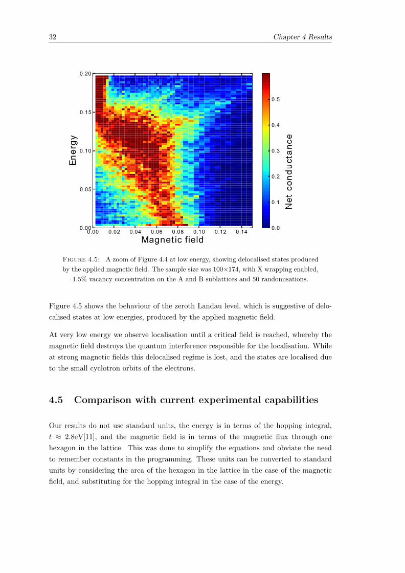
4.5 A zoom of Figure 4.4 at low energy, showing delocalised states producedby the applied magnetic field. The sample size was 100×174, with Xwrapping enabled, 1.5% vacancy concentration on the A and B sublatticesand 50 randomisations. . . . . . . . . . . . . . . . . . . . . . . . . . . . . . 32
Chapter 1
Introduction
Graphene is an allotrope of carbon consisting of carbon atoms in a two-dimensional,
bipartite lattice consisting of two interpenetrating triangular sublattices. Graphene was
first isolated in 2004 by Geim, Novoselov and their colleagues[2], and was the first
2D crystal to be successfully isolated. They demonstrated its interesting electronic
properties and, since then, interest in graphene has flourished.
In their initial work, Geim et al. isolated graphene through the micromechanical exfoli-
ation of graphite. Sticky tape was used to repeatedly peel layers of carbon atoms from
a graphite sample until only a single layer remained on the sticky tape. The carbon
flakes were then transferred to a Silicon Dioxide substrate where the graphene flakes
were detected with an optical microscope due to the interference they produce when
on the substrate[3]. However, new methods of isolation for mass production, such as
Chemical Vapour Deposition, are now being pursued[4]. This means that understanding
graphene’s electrical properties is an urgent and vital research effort.
Graphene has a remarkable number of theoretically interesting phenomena. The quasi-
particles act as massless Dirac fermions near the Dirac points, and so demonstrate
relativistic behaviour, such as the unintuitive Klein Paradox[5]. The suppression of
localisation also leads to the apparent universal minimum conductivity (the so-called
“conductivity without charge carriers”[6]), meanwhile the origin of the missing Pi prob-
lem, where the experimental value of the minimum conductivity is observed to be an
order of pi larger than the theoretical value, remains unclear[6].
Due to its unique electrical properties, graphene has a huge range of prospective ap-
plications from mass sensors[7], to photodectectors[8] and high frequency transistors[9].
However, graphene field effect transistors currently have low on-off ratios, meaning the
transistors cannot be turned off effectively. This may be overcome by creating a band
gap in the sample, for example, by doping with hydrogen to produce graphane[10]. Our
theoretical investigation in to the effects of magnetic field and doping in graphene is
relevant to these practical problems.
1

2 Chapter 1 Introduction
Our work focussed on investigating the effects of doping and magnetic field on the
conduction in monolayer graphene samples. A numerical model was developed using
fortran 77 and the lapack linear algebra package, so that the effects of magnetic
field and vacancy concentration could be investigated.
Chapter 2
Background Theory
This chapter details several aspects of the background theory regarding graphene, which
are relevant to the methods we have used and the analysis of our results.
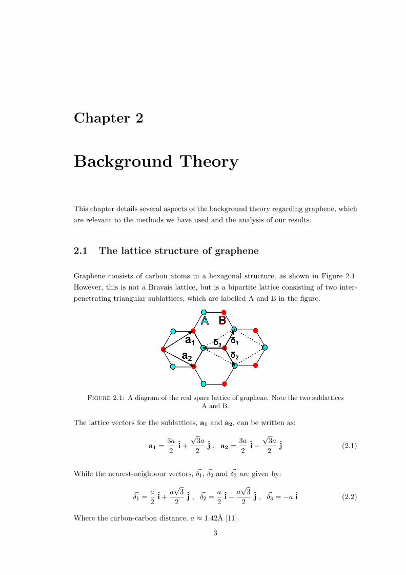
2.1 The lattice structure of graphene
Graphene consists of carbon atoms in a hexagonal structure, as shown in Figure 2.1.
However, this is not a Bravais lattice, but is a bipartite lattice consisting of two inter-
penetrating triangular sublattices, which are labelled A and B in the figure.
Figure 2.1: A diagram of the real space lattice of graphene. Note the two sublatticesA and B.
The lattice vectors for the sublattices, a1 and a2, can be written as:
a1 =3a
2i +
√3a
2j , a2 =
3a
2i−√
3a
2j (2.1)
While the nearest-neighbour vectors, ~δ1, ~δ2 and ~δ3 are given by:
~δ1 =a
2i +
a√
3
2j , ~δ2 =
a
2i− a
√3
2j , ~δ3 = −a i (2.2)
Where the carbon-carbon distance, a ≈ 1.42A [11].
3
4 Chapter 2 Background Theory
2.2 The Tight Binding approximation
The Tight Binding approximation assumes the electrons are tightly bound to their cor-
responding atoms, and so the electrons can only reside at lattice sites.
In this work, only nearest neighbour hopping is taken in to account, and so electrons
can only move from a site on sublattice A to a site on sublattice B and vice versa. This
is an acceptable approximation as the next nearest neighbour hopping energy is only
approximately 3.5% of the value of the nearest neighbour hopping energy[11], and so
there is no major loss of information for the additional simplicity.
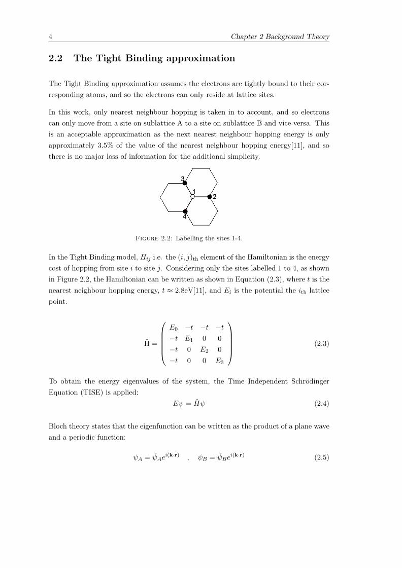
Figure 2.2: Labelling the sites 1-4.
In the Tight Binding model, Hij i.e. the (i, j)th element of the Hamiltonian is the energy
cost of hopping from site i to site j. Considering only the sites labelled 1 to 4, as shown
in Figure 2.2, the Hamiltonian can be written as shown in Equation (2.3), where t is the
nearest neighbour hopping energy, t ≈ 2.8eV[11], and Ei is the potential the ith lattice
point.
H =
E0 −t −t −t−t E1 0 0
−t 0 E2 0
−t 0 0 E3
(2.3)
To obtain the energy eigenvalues of the system, the Time Independent Schrodinger
Equation (TISE) is applied:
Eψ = Hψ (2.4)
Bloch theory states that the eigenfunction can be written as the product of a plane wave
and a periodic function:
ψA = ψAei(k·r) , ψB = ψBe
i(k·r) (2.5)
Chapter 2 Background Theory 5
So by substituting Equation (2.5) in to Equation (2.4), with r having its origin at point
1, the TISE can be written as:
EψA = −∑i,j
Hijψj = H12ψ2 +H13ψ3 +H14ψ4 = −t(ψ2 + ψ3 + ψ4) (2.6)
But k · r in Equation (2.5) can be expressed as:
k · r = kxx+ kyy (2.7)
By writing the wavefunctions in terms of Bloch waves (Equation (2.5)), substituting in
the lattice vectors and wave vectors from Equation (2.7), and expressing the TISE in
terms of the non-zero elements of the Hamiltonian (as in Equation (2.6)), the TISE can
be written as:
EψA = −tψB
(exp (ikxa) + exp
(−ikxa
2+ikya√
3
2
)+ exp
(−ikxa
2− ikya
√3
2
))= −t(k)ψB (2.8)
Repeating the process for a point on sublattice B, and combining the equations obtains
the complete expression for the TISE of the system:
Eψ =
(0 −t(k)
−t∗(k) 0
)ψ (2.9)
Taking the eigenvalues of this matrix obtains the energy eigenvalues of the system:
E = ±∣∣t(k)
∣∣ (2.10)
2.3 Dirac points and the linear dispersion relation
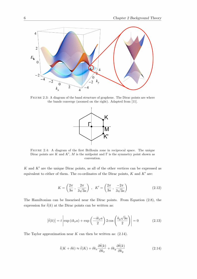
Figure 2.3 is a plot of the electronic band structure of graphene. The Dirac points are
where the bands converge, their points in k-space given by the condition in Equation
(2.11). In undoped graphene, the Fermi level lies across the Dirac points
∣∣t(k)∣∣ = 0 (2.11)
In reciprocal space, the Dirac points lie on the vertices of the first Brillouin Zone (i.e.
the Wigner-Seitz cell of the reciprocal lattice) as shown in Figure 2.4.
6 Chapter 2 Background Theory
Figure 2.3: A diagram of the band structure of graphene. The Dirac points are wherethe bands converge (zoomed on the right). Adapted from [11].
Figure 2.4: A diagram of the first Brillouin zone in reciprocal space. The uniqueDirac points are K and K ′, M is the midpoint and Γ is the symmetry point shown as
convention.
K and K ′ are the unique Dirac points, as all of the other vertices can be expressed as
equivalent to either of them. The co-ordinates of the Dirac points, K and K ′ are:
K =
(2π
3a,
2π
3√
3a
), K ′ =
(2π
3a,−2π
3√
3a
)(2.12)
The Hamiltonian can be linearised near the Dirac points. From Equation (2.8), the
expression for t(k) at the Dirac points can be written as:
∣∣t(k)∣∣ = t
∣∣∣∣∣exp (ikxa) + exp
(−ikxa
2
)2 cos
(ky√
3a
2
)∣∣∣∣∣ = 0 (2.13)
The Taylor approximation near K can then be written as: (2.14).
t(K + δk) ≈ t(K) + δkx∂t(k)
∂kx+ δky
∂t(k)
∂ky(2.14)
Chapter 2 Background Theory 7
Calculating the differentials, and substituting the expression for K from Equation (2.12),
t(k) near K can be expressed as:
t(K + δk) ≈ 3ati
2δkx +
3at
2δky (2.15)
Substituting this in to Equation (2.9), yields the expression for the Hamiltonian near
K:
HK(k) =3at
2
(0 −ky − ikx
−ky + ikx 0
)(2.16)
This can be written in terms of the Pauli matrices by rotating the k-vector, so kx is
replaced with ky and ky is replaced with −kx, producing the expression in Equation
(2.17).
HK(k) =3at
2~σ · ~k (2.17)
By the same consideration, the expression for the Hamiltonian near K ′ in Equation
(2.18) can be derived.
HK′(k) =−3at
2~σ∗ · ~k (2.18)
Taking the eigenvalues of the Hamiltonian near K or K ′ obtains the linear dispersion
relation:
ε =3at
2k = v~k (2.19)
The linear dispersion relation means the quasiparticles are massless Dirac fermions with
constant velocity v (where v ≈ 106 m s−1)[11]. This is relevant for the transport proper-
ties of graphene, as all quantum transport occurs near the Dirac points since the Fermi
energy is low in comparison with the local peak energy (where the linear approximation
breaks down) of t ≈ 2.8eV[11], which corresponds to a Fermi temperature of approxi-
mately 30,000K.
The t values were determined from cyclotron resonance experiments, which provide
experimental evidence for the linear dispersion relation in graphene[12].
It can also be shown that the density of states has a linear dependence with respect
to energy near the Dirac point, using the dispersion relation. The area of each allowed
8 Chapter 2 Background Theory
k-state is:
Ak =
(2π
a
)2
(2.20)
So considering a circle of area πk2 in reciprocal space, one obtains:
N(k) =4πk2(2πa
)2 =k2a2
π=Ak2
π(2.21)
Substituting the dispersion relation (Equation (2.19)) obtains:
N(E) =AE2
πv2~2(2.22)
And differentiating to obtain the density of states near the Dirac points:
g(E) =N(E)
dE=
2AE
πv2~2∝ E (2.23)
2.4 Density of states
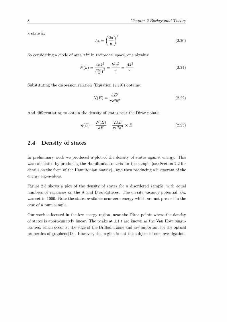
In preliminary work we produced a plot of the density of states against energy. This
was calculated by producing the Hamiltonian matrix for the sample (see Section 2.2 for
details on the form of the Hamiltonian matrix) , and then producing a histogram of the
energy eigenvalues.
Figure 2.5 shows a plot of the density of states for a disordered sample, with equal
numbers of vacancies on the A and B sublattices. The on-site vacancy potential, U0,
was set to 1000. Note the states available near zero energy which are not present in the
case of a pure sample.
Our work is focused in the low-energy region, near the Dirac points where the density
of states is approximately linear. The peaks at ±1 t are known as the Van Hove singu-
larities, which occur at the edge of the Brillouin zone and are important for the optical
properties of graphene[13]. However, this region is not the subject of our investigation.
Chapter 2 Background Theory 9
-3 -2 -1 0 1 2 3Energy (t)
0
20
40
60
80
100
Fre
quen
cy
Figure 2.5: A plot of the density of states for a 50×86 sample with 3% vacancy
concentration on the A and B sublattices and 50 randomisations.
2.5 The Klein Effect
The Klein Effect is a consequence of the linear dispersion of the massless quasiparticles.
It is the counterintuitive result that in the case of quantum tunneling across a potential
barrier, the transmission probability increase with the height of the potential barrier,
and tends to 1 as the potential tends to infinity[5]. It is this effect that makes undoped
graphene difficult to use in electronic devices.
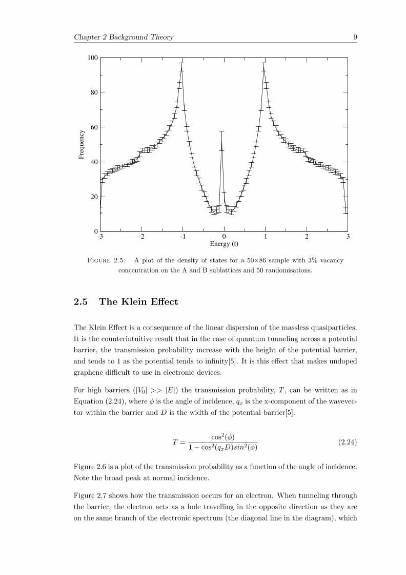
For high barriers (|V0| >> |E|) the transmission probability, T , can be written as in
Equation (2.24), where φ is the angle of incidence, qx is the x-component of the wavevec-
tor within the barrier and D is the width of the potential barrier[5].
T =cos2(φ)
1− cos2(qxD)sin2(φ)(2.24)
Figure 2.6 is a plot of the transmission probability as a function of the angle of incidence.
Note the broad peak at normal incidence.
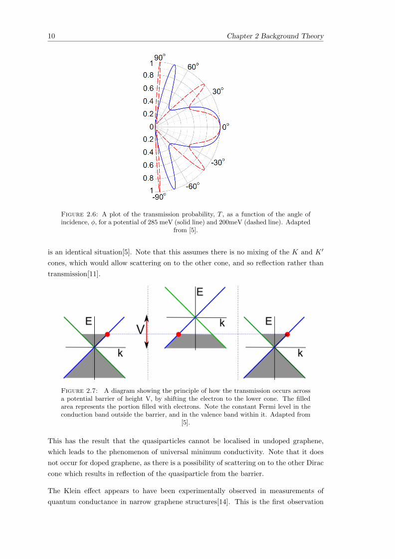
Figure 2.7 shows how the transmission occurs for an electron. When tunneling through
the barrier, the electron acts as a hole travelling in the opposite direction as they are
on the same branch of the electronic spectrum (the diagonal line in the diagram), which
10 Chapter 2 Background Theory
Figure 2.6: A plot of the transmission probability, T , as a function of the angle ofincidence, φ, for a potential of 285 meV (solid line) and 200meV (dashed line). Adapted
from [5].
is an identical situation[5]. Note that this assumes there is no mixing of the K and K ′
cones, which would allow scattering on to the other cone, and so reflection rather than
transmission[11].
Figure 2.7: A diagram showing the principle of how the transmission occurs acrossa potential barrier of height V, by shifting the electron to the lower cone. The filledarea represents the portion filled with electrons. Note the constant Fermi level in theconduction band outside the barrier, and in the valence band within it. Adapted from
[5].
This has the result that the quasiparticles cannot be localised in undoped graphene,
which leads to the phenomenon of universal minimum conductivity. Note that it does
not occur for doped graphene, as there is a possibility of scattering on to the other Dirac
cone which results in reflection of the quasiparticle from the barrier.
The Klein effect appears to have been experimentally observed in measurements of
quantum conductance in narrow graphene structures[14]. This is the first observation
Chapter 2 Background Theory 11
of the Klein effect.
2.6 The Landauer Formula
The Landauer Formula is used to calculate the conductance of the sample. The equation
for the net conductance, Equation (2.25), is derived by considering the electrons that
are able to move across a potential, with respect to the Fermi-Dirac distribution[15]. G
is the net conductance of the sample, and Ti is the transmission coefficient for the ith
channel to take in to account varying transmission coefficients.
G ≈ e2
π~∑i
Ti (2.25)
The per channel conductivity is given in Equation (2.26). Note that there is no temper-
ature dependence, and so this means there is a minimum conductivity even in undoped
graphene at low temperatures when normal semiconductors become insulators[6]. This
is a remarkable and unintuitive property of graphene when compared with other semi-
conductors.
σ ≈ e2
π~(2.26)
However, when the minimum conductivity was measured experimentally, it was found
to be an order of π larger. This is known as the “Missing Pi Problem” and the ex-
act reason for the discrepancy remains unknown[6]. However, experimental work by
Miao et al. in 2007 reported that the experimental value of the minimum conductivity
approached the theoretical value for small, wide rectangles of graphene, after testing
various rectangles[16].
2.7 The Quantum Hall Effect
The quantum Hall effect is the phenomenon whereby the Hall conductivity is observed
to be quantised in to a series of plateaus. In the standard integer quantum Hall effect,
the Hall conductivity is given by Equation (2.27), where σxy is the Hall conductivity
and ν is the filling factor which is a non-zero integer in this integer case[17].
σxy = νe2
h(2.27)
12 Chapter 2 Background Theory
Landau quantisation is the quantisation of the orbits of charged particles in a magnetic
field. This results in Landau levels which are levels of constant energy consisting of
many degenerate states[18]. The quantum Hall effect is observed under strong magnetic
fields, when the number of degenerate states per Landau level is high. The equation for
the number of degenerate states in a Landau level is given in Equation (2.28), where gs
is the spin degeneracy factor, B is the magnitude of the applied magnetic field, A is the
area of the sample and φ0 is the quantum of the magnetic flux[18].
Nd =gsBA
φ0(2.28)
The electrons fill up the Landau levels in order of increasing energy[18]. It is only
at the transitions between Landau levels that the quantised energy of the cyclotron
orbit changes, and so the Hall conductivity can increase, and so plateaus with steps are
produced. The density of states peaks at the steps between Landau levels, whilst being
zero elsewhere, and so the longitudinal resistivity peaks at these points. Disorder has
the effect of broadening these peaks, eventually destroying the plateau structure at large
disorder[18].
In graphene, the quantum Hall effect takes a “half-integer” form, so the plateaus have
the expected step height but the sequence is shifted by a half[19]. The equation for the
Hall conductivity then takes the form in Equation (2.29), where the factor of 4 occurs
due to double spin degeneracy from the actual spin and pseudo-spin (describing the
current sublattice of the electron)[19].
σxy =4e2
h
(±N +
1
2
)(2.29)
The anomalous shift in the sequence of σxy plateaus in graphene is a result of the
presence of the zero energy level, which draws half of its electrons from the valence band
and half from the conduction band[3]. This state itself is a result of the linear dispersion
relation of graphene in a magnetic field, which is described by Equation (2.30), where
the ± factor represents electrons and holes, N is an integer, B is the magnitude of the
applied magnetic field and vF is the constant velocity of the Dirac fermions[19].
EN = ±vF√
2e~BN (2.30)
A plot of the Hall conductivity in graphene calculated from theory is shown in Figure
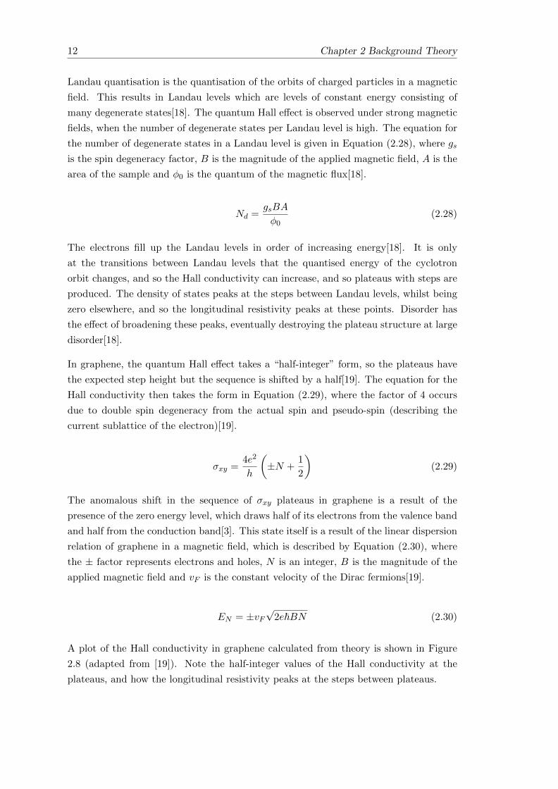
2.8 (adapted from [19]). Note the half-integer values of the Hall conductivity at the
plateaus, and how the longitudinal resistivity peaks at the steps between plateaus.
Chapter 2 Background Theory 13
Figure 2.8: A theoretical graph of the Hall conductivity (right axis, plateaus line)
and longitudinal resistivity (left axis, peaks line) in monolayer graphene. Note the half-
integer values of the Hall-conductivity and the peaks of the longitudinal resistivity at
the plateau steps. Adapted from [19].
2.8 Localisation
Localised states which are defined as the states whose wavefunctions are concentrated
mainly in a confined region and exponentially decay outside of this region[20]. Localised
electrons are confined to specific sites, and cannot contribute to the net conduction of
the sample. In contrast, delocalised electrons can move through-out the sample, and so
contribute to conduction.
The scaling theory of localisation models localisation by considering the dimensionless
conductance as a function of scale variables, such as the system size, L. In the delocalised
phase in a 2-dimensional system, the conductance is independent of system size[21].
g(L) ∼ σ (2.31)
Where σ is the conductivity of the sample.
14 Chapter 2 Background Theory
In the localised phase, however, conduction occurs by tunneling between states of ap-
proximately equal energy. This results in an exponentially decaying behaviour for the
conductance with respect to system size[21]:
g(L) ∼ e−Lξ (2.32)
Where L is the sample size, and ξ is the localisation length. Note that the limit of large
localisation length (ξ >> L) tends towards the delocalised case.
Chapter 3
Method and Implementation
This chapter details the method which were used to develop the numerical model, and
the specifics of the implementation. The model was written in fortran 77 using the
lapack linear algebra package for the matrix calculations. The source code is freely
available on Github[22]. A simplified flowchart of the program’s operation is given in
Appendix A.
A computational approach is necessary in order to model the disorder, as it allows a
Monte Carlo approach to be used: producing and averaging many randomised disorder
configurations. The computational time required to run the calculations is significant,
even with some optimisations that were made, running 50 lattice randomisations over
100 energy values for a lattice size of 100×174 requires about 12 hours, depending
on the hardware. The slowest parts of the calculations are the matrix inversions and
multiplications which are of order O(n3), so some efforts were made to split and reduce
the size of the matrices where possible.
3.1 Representation of the graphene sample
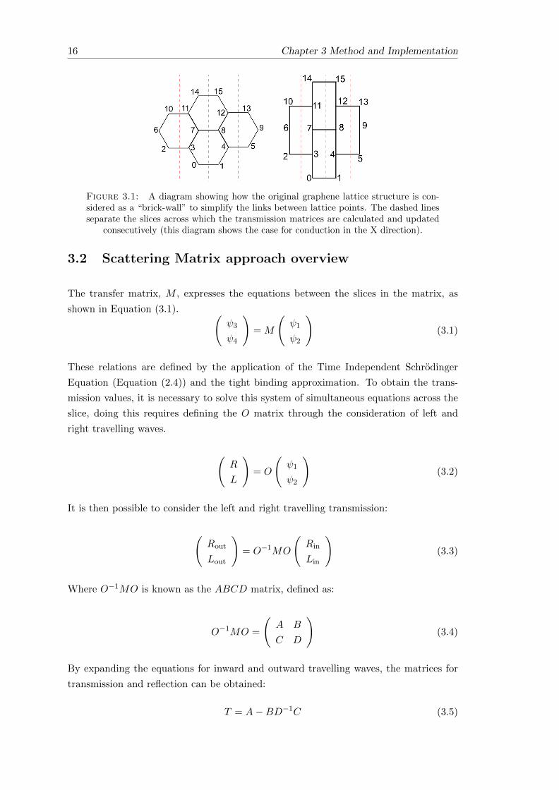
In the model, the honeycomb lattice is translated to a “brick-wall” model, as shown in
Figure 3.1, for the calculations. This means that to obtain a square lattice in real space,
the vertical size must equal the horizontal size multiplied by√
3 due to the change in
shape of the real lattice.
The transmission matrices are calculated across each slice consecutively, updating the
net sample transmission matrices progressively. This was implemented as it is more
efficient than solving the equations for a single, large net transfer matrix.
15
16 Chapter 3 Method and Implementation
Figure 3.1: A diagram showing how the original graphene lattice structure is con-sidered as a “brick-wall” to simplify the links between lattice points. The dashed linesseparate the slices across which the transmission matrices are calculated and updated
consecutively (this diagram shows the case for conduction in the X direction).
3.2 Scattering Matrix approach overview
The transfer matrix, M , expresses the equations between the slices in the matrix, as
shown in Equation (3.1). (ψ3
ψ4
)= M
(ψ1
ψ2
)(3.1)
These relations are defined by the application of the Time Independent Schrodinger
Equation (Equation (2.4)) and the tight binding approximation. To obtain the trans-
mission values, it is necessary to solve this system of simultaneous equations across the
slice, doing this requires defining the O matrix through the consideration of left and
right travelling waves.
(R
L
)= O
(ψ1
ψ2
)(3.2)
It is then possible to consider the left and right travelling transmission:
(Rout
Lout
)= O−1MO
(Rin
Lin
)(3.3)
Where O−1MO is known as the ABCD matrix, defined as:
O−1MO =
(A B
C D
)(3.4)
By expanding the equations for inward and outward travelling waves, the matrices for
transmission and reflection can be obtained:
T = A−BD−1C (3.5)
Chapter 3 Method and Implementation 17
T = D−1 (3.6)
R = BD−1C (3.7)
R = −D−1C (3.8)
Where T and R define the transmission and reflection in the forward-travelling case,
and T and R define the transmission and reflection in the backward-travelling case.
These matrices are calculated for each slice and the net matrices are updated. The
transmission values themselves are then obtained by using Singular Value Decomposition
on these matrices. The net conductance is simply the sum of the transmission values.
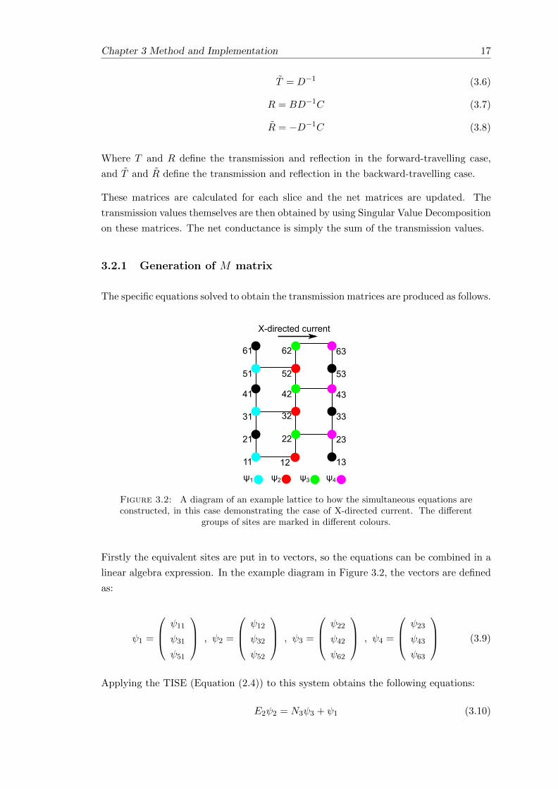
3.2.1 Generation of M matrix
The specific equations solved to obtain the transmission matrices are produced as follows.
11 12 13
23
33
43
53
63
21
31
41
51
61
22
32
42
52
62
X-directed current
ψ1 ψ2 ψ3 ψ4
Figure 3.2: A diagram of an example lattice to how the simultaneous equations areconstructed, in this case demonstrating the case of X-directed current. The different
groups of sites are marked in different colours.
Firstly the equivalent sites are put in to vectors, so the equations can be combined in a
linear algebra expression. In the example diagram in Figure 3.2, the vectors are defined
as:
ψ1 =
ψ11
ψ31
ψ51
, ψ2 =
ψ12
ψ32
ψ52
, ψ3 =
ψ22
ψ42
ψ62
, ψ4 =
ψ23
ψ43
ψ63
(3.9)
Applying the TISE (Equation (2.4)) to this system obtains the following equations:
E2ψ2 = N3ψ3 + ψ1 (3.10)
18 Chapter 3 Method and Implementation
E3ψ3 = N2ψ2 + ψ4 (3.11)
Where E2 and E3 are the (E − V ) vectors (i.e. the energy minus the site potential) for
the sites in the ψ2 and ψ3 vectors respectively, and N2 and N3 are matrices which define
the links between the sites, in this case defined as:
N3 =
1 0 0
1 1 0
0 1 1
, N2 =
1 1 0
0 1 1
0 0 1
(3.12)
Enabling wrapping simply adds wrapped links in the X direction, making the appropriate
changes to the N{2,3} matrices. However note that to use X-wrapping, the sample size
in the X direction must be a multiple of 2 in order to obtain a physical system. This
check is present in our program.
Solving these equations for the transfer matrix, M , obtains the following block matrix:
M =
(−N−13 E2N
−13
−E3N−13 E2E3N
−13 −N2
)(3.13)
It is this matrix which is produced and used in Equation (3.4) to calculate the trans-
mission matrices.
In the case without magnetic field, the O matrix is simply defined by the block matrix:
O =1√2
(1 1
i −i
)(3.14)
This can be derived by consideration of the probability current.
3.2.2 Updating transmission matrices
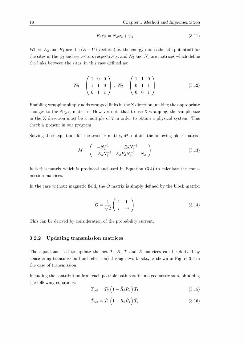
The equations used to update the net T , R, T and R matrices can be derived by
considering transmission (and reflection) through two blocks, as shown in Figure 3.3 in
the case of transmission.
Including the contribution from each possible path results in a geometric sum, obtaining
the following equations:
Tnet = T2
(1− R1R2
)T1 (3.15)
Tnet = T1
(1−R2R1
)T2 (3.16)
Chapter 3 Method and Implementation 19
T1 R1 T2 R2T2T1
T2R1R2T1
~
T2R1R2R1R2T1
~ ~
Figure 3.3: A diagram showing the net transmission across two blocks. One mustinclude the contributions from all of the possible paths, resulting in a geometric sum.
Rnet = R1 + T1
(1−R2R1
)−1R2T1 (3.17)
Rnet = R2 + T2
(1− R1R2
)−1R1T2 (3.18)
It is these equations which are used to update the net transmission matrices.
3.3 Tests of correctness
3.3.1 Unitarity checking
The first test, built in to the software, is calculating the unitarity of the net transmission
matrices, checking that the following condition holds:(T R
R T
)†(T R
R T
)= I (3.19)
The Frobenius norm (square root of the squared sums) of the off-diagonal elements
is calculated, and checked to be close to zero (values less than 10−6 were considered
acceptable). For efficiency reasons this check is actually implemented in terms of the
transmission matrices themselves. The following conditions are checked, and the results
are combined.
T †T +R†R = 1 (3.20)
T †T + R†R = 1 (3.21)
T †R+R†T = 0 (3.22)
This provides a quick check that the linear algebra calculations are behaving as expected,
but it does not prove that the results are physical in itself. To this end, we also tested
results against analytical equations which we produced.
20 Chapter 3 Method and Implementation
3.3.2 Analytical tests
By considering the net matrix across a pure sample, it is possible to obtain an analytical
solution for the transmission values (and so conductance). This is done by writing the
recurrence relations as a finite difference equation.
Figure 3.4: A diagram of the “ladder” configuration for which the analytical testswere derived.
For example, in the case of Y-directed conduction down a vertical “ladder” (i.e. where
the horizontal length is 2), one can define two transfer matrices (calculated as explained
in Section 3.2.1) for odd (no horizontal link) and even (linked) steps (note that in the
case of x-wrapping these would simply be equal to one another).
Meven =
0 0 1 0
0 0 0 1
−1 0 E 0
0 −1 0 E
, Modd =
0 0 1 0
0 0 0 1
−1 0 E −1
0 −1 −1 E
(3.23)
For one step down the sample, one obtains:
MevenModd =
−1 0 E −1
0 −1 −1 E
−E 0 E2 − 1 −E0 −E −E E2 − 1
=
(an bn
cn dn
)(3.24)
Meven and Modd can also be written in terms of block matrices:
Meven =
(0 1
−1 E
), Modd =
(0 1
−1 λ
)(3.25)
Where λ = E ± 1 (note in the case of X-wrapping then λ = E). Considering pairs of
steps one obtains the following block matrices for the initial and second steps.
M =
(−1 λ
−E Eλ− 1
), M2 =
(1− Eλ λ(Eλ− 1)− λ
E − E(Eλ− 1) (Eλ− 1)2 − Eλ
)(3.26)
Chapter 3 Method and Implementation 21
The eigenvalues of M are:
ξ =1
2
(Eλ− 2−
√E2λ2 − 4Eλ
)(3.27)
1
ξ=
1
2
(Eλ− 2 +
√E2λ2 − 4Eλ
)(3.28)
It is now possible to solve the following recursion relations to obtain the coefficients
for the general recurrence relation, since the matrix elements can be expressed as a
combination of the initial eigenvalues:
α1 + α2 = 1 α1ξ +α2
ξ= −1 (3.29)
β1 + β2 = 1 β1ξ +β2ξ
= λ (3.30)
γ1 + γ2 = 0 γ1ξ +γ2ξ
= −E (3.31)
δ1 + δ2 = 1 δ1ξ +δ2ξ
= Eλ− 1 (3.32)
Solving these simultaneous equations for the coefficients (in Greek letters) results in the
following equations for the submatrix blocks:
an =
(1− −(1 + ξ)
1ξ − 1
)ξn +
−(1 + ξ)
ξn(1ξ − 1
) (3.33)
bn =λξn
ξ − 1ξ
− λ
ξn(ξ − 1
ξ
) (3.34)
cn =−Eξn
ξ − 1ξ
+E
ξn(ξ − 1
ξ
) (3.35)
dn =
(Eλ− 1− 1
ξ
ξ − 1ξ
)ξn +
(1−
(Eλ− 1− 1
ξ
ξ − 1ξ
))1
ξn(3.36)
Calculating the general form of O−1MO obtains the following equations for the trans-
mission and reflection values:
T =2
(a+ d) + (c− b)i= T (3.37)
R =(a− d) + (b+ c)i
(a+ d) + (c− b)i(3.38)
R =(a− d)− (b+ c)i
(a+ d) + (c− b)i(3.39)
22 Chapter 3 Method and Implementation
Equation (3.37) is used to calculate the transmission values. Substituting in the relations
and simplifying the results obtains the following equations:
In the case of real ξ:
T =2
(ξn + ξ−n) + −E−λξ−ξ−1 (ξn − ξ−n) i
(3.40)
Where ξ is defined by:
ξ =Eλ
2− 1−
√E2λ2
4− Eλ (3.41)
Note that since λ = E ± 1, ξ can be both real and complex. In the case of complex ξ:
T =2
2 cos(nφ) + −E−λsin(φ) (ξn − ξ−n) i
(3.42)
With the following definitions for φ:
cos(φ) =Eλ
2− 1 , sin(φ) = −
√Eλ− E2λ2
4(3.43)
A plot of the results from these analytical equations and the program output is shown
in Figure 3.5 for the 2×4 ladder. The program output and analytical results matched,
and this was also tested for various lengths of ladders. The source code for this program
is given in Appendix B.1. The same check was also repeated for a horizontal chain with
X-directed current.
Chapter 3 Method and Implementation 23
−4 −2 0 2 4
0.0
0.2
0.4
0.6
0.8
1.0
Energy (t)
T2 v
alu
eModel output
Analytical result
Model output
Analytical result
Figure 3.5: A plot of the results of the analytical equations against the program
output for a 2×4 lattice, with conduction in the Y-direction as shown in Figure 3.4.
The squares of the transmission values are plotted against the energy. The circles are
the program output, and the lines are the analytical results. Note there are two T
values since the (horizontal) width is 2. The net conductance is simply the sum of the
transmission values.
3.4 Implementation of magnetic field
The addition of magnetic field introduces a phase factor in to the N{2,3} matrices de-
scribed in Subsection 3.2.1.
So, in the case of the magnetic vector potential being directed in the Y-direction, and
so varying in the X-direction the 1’s in the matrices must be replaced by a phase factor
e±iφxn where φ is the magnetic flux and xn is the column number of the lattice site.
The addition of magnetic field also requires that the O matrix is modified in the case
where the current and magnetic vector potential are directed in the same direction. For
efficiency reasons the O matrix was split up and defined in terms of a u submatrix, as
follows:
24 Chapter 3 Method and Implementation
O =1√2
(1 1
u −u
)(3.44)
Where u = i in the case of no magnetic field.
In this case, u must take in to account the phase factor, so if Y-directed magnetic vector
potential is applied to the ladder example in Subsection 3.3.2 then:
u =
(ieiφ 0
0 ie2iφ
)(3.45)
Note that to convert from the flux to the magnetic field, we must consider the area of
the hexagons, resulting in the following equation:
B =4φ
3√
3(3.46)
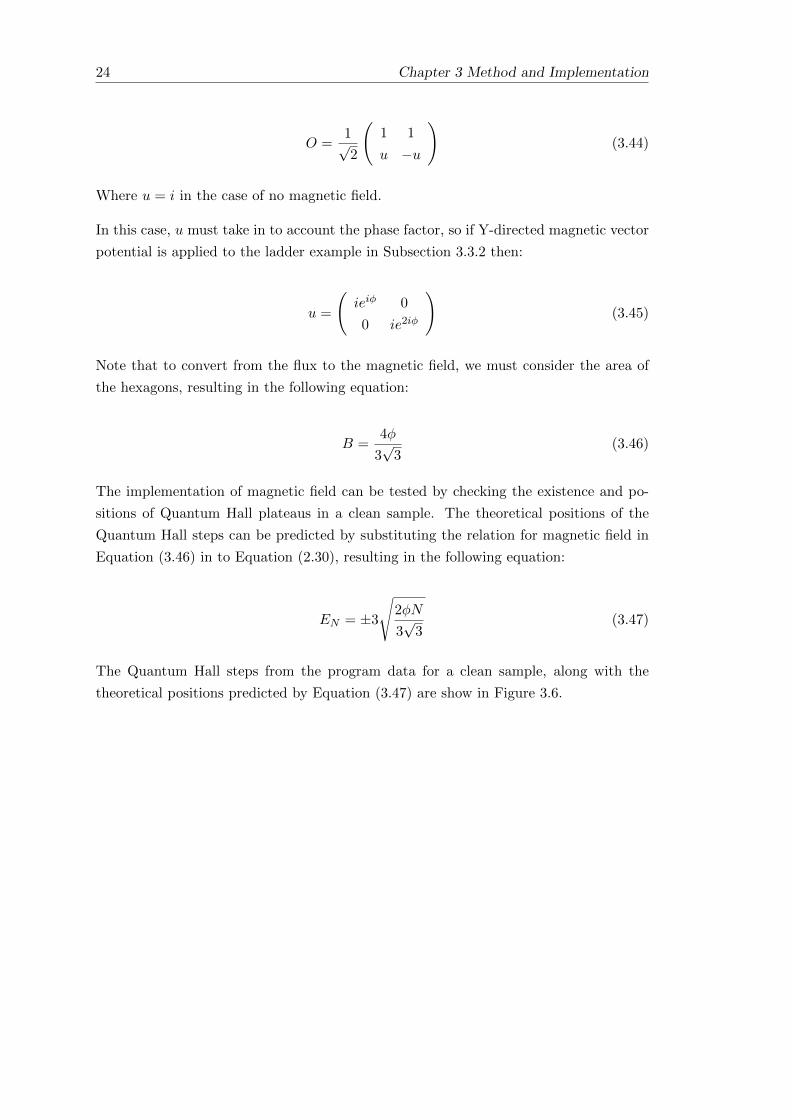
The implementation of magnetic field can be tested by checking the existence and po-
sitions of Quantum Hall plateaus in a clean sample. The theoretical positions of the
Quantum Hall steps can be predicted by substituting the relation for magnetic field in
Equation (3.46) in to Equation (2.30), resulting in the following equation:
EN = ±3
√2φN
3√
3(3.47)
The Quantum Hall steps from the program data for a clean sample, along with the
theoretical positions predicted by Equation (3.47) are show in Figure 3.6.
Chapter 3 Method and Implementation 25
0 0.1 0.2 0.3 0.4 0.5Energy
0
1
2
3
4
5
6
7
8
9
10
Conduct
ance
Unwrapped conductance
Modified wrapped conductance, 0.1*(log(G)+150)
Figure 3.6: A plot of the quantum Hall steps in the wrapped and unwrapped
conductance for a 160×277 sample, with the current in the X-direction and magnetic
vector potential in the Y-direction, at a flux of 0.0227. The wrapped conductance is
appropriately modified so it can be viewed on the same scale. The theoretical values of
the QHE steps are shown with dotted lines.
3.5 Implementation of disorder
Disorder is implemented by simulating electronic vacancies on the lattice sites, which
could be created experimentally, through the addition of adatoms such as Hydrogen,
which bond to the sites. The vacancies themselves are implemented by setting the
on-site lattice potential, U0 to a high, finite value (in our results U0 = 1000 was used).
A Monte Carlo approach is used to calculate the results for specified disorder concen-
trations on the A and B sublattices. This means that the lattice is repeatedly generated
with randomised positions of vacancies and the results are averaged across all randomly
generated lattices.
To achieve this the random number generator ran2 from Numerical Recipes in Fortran
77 [23] was used. A fixed number of vacancies is then calculated from the given vacancy
concentration and lattice size. Random sites are then chosen and, if all the vacancies for

26 Chapter 3 Method and Implementation
that sublattice have not yet been allocated, made in to a vacancy. If they are already a
vacancy then they are skipped and a new random site is generated. The source code for
this is given in Appendix B.2. The standard error of the repeated randomised samples
is also calculated to provide an indication of the reliability of the results. It was found
that 50 repeats gave a good trade-off between computation time and reliability.
Chapter 4
Results
This chapter covers the main results from the data which we have produced from the
program. Square lattices were used in order to ensure there are no effects from 1-
dimensional effects. X-directed current and Y-directed magnetic vector potential were
used, as this is slightly more efficient, since in the case of the X-directed current the
matrices only have a rank of LIMY2 , and having them directed in different directions
means that the u matrix does not have to be modified for magnetic field (see Section
3.4).
27
28 Chapter 4 Results
4.1 Size effects
-0.5 -0.4 -0.3 -0.2 -0.1 0 0.1 0.2 0.3 0.4 0.5Energy
0.01
0.1
1
Con
duct
ance
50x86 76x132100x174124x214150x260200x346
Plot of G against E, Unwrapped samples0.015 vac conc A and B, 350 randomisations
Figure 4.1: Conductance for various sizes of square samples, showing the transition
from the delocalised to the localised regime near E = ± 0.2
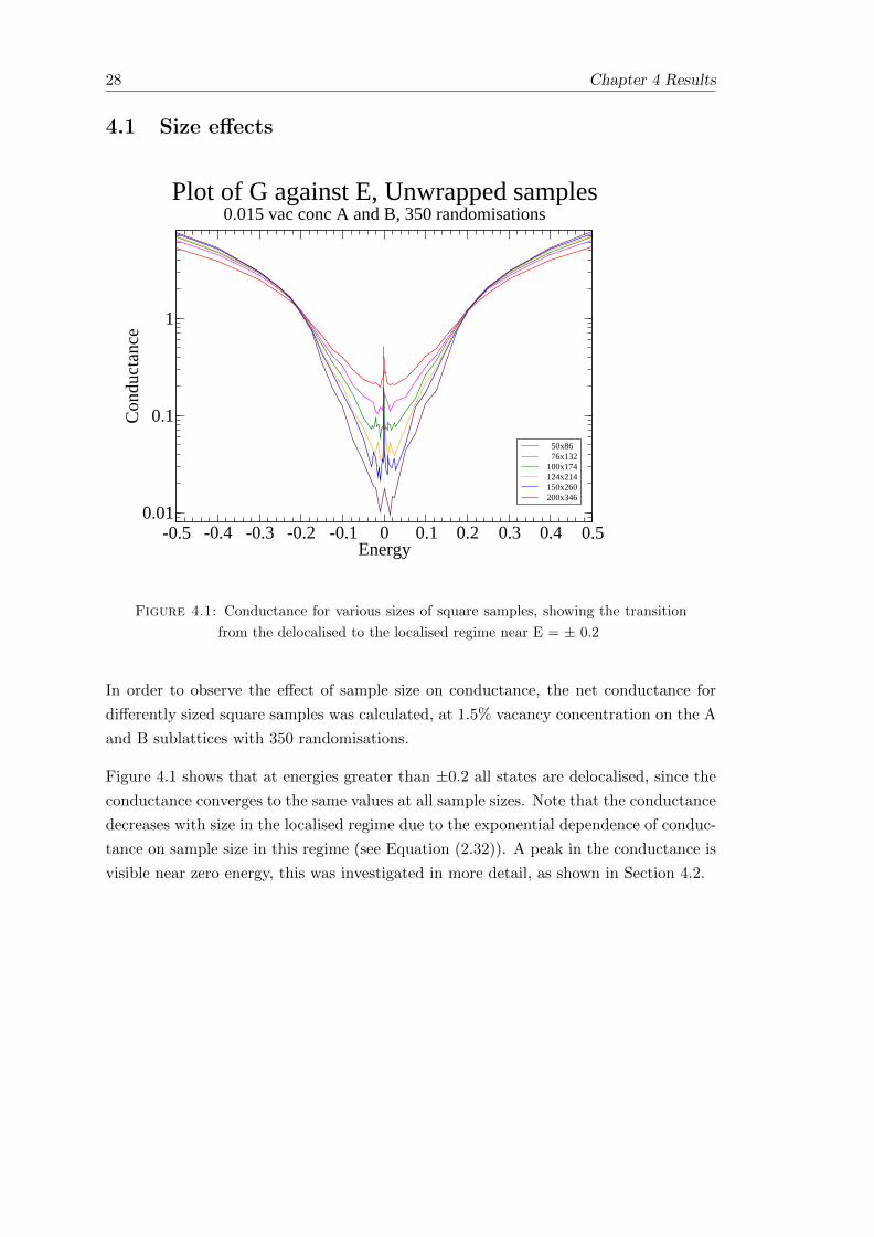
In order to observe the effect of sample size on conductance, the net conductance for
differently sized square samples was calculated, at 1.5% vacancy concentration on the A
and B sublattices with 350 randomisations.
Figure 4.1 shows that at energies greater than ±0.2 all states are delocalised, since the
conductance converges to the same values at all sample sizes. Note that the conductance
decreases with size in the localised regime due to the exponential dependence of conduc-
tance on sample size in this regime (see Equation (2.32)). A peak in the conductance is
visible near zero energy, this was investigated in more detail, as shown in Section 4.2.
Chapter 4 Results 29
4.2 Zero energy conductance peak
-0.008 -0.004 0 0.004 0.008Energy
0.01
0.1
Con
duct
ance
50x86100x174150x260
Plot of G against E, Unwrapped samples0.015 vac conc A and B, 350 randomisations
Figure 4.2: A zoomed plot of the central, low energy region of Figure 4.1 showing
the conductance peak at E= −10−3 .
The zero-energy peak visible in Figure 4.1 was investigated in more detail at a much
higher energy resolution. The resolution was lowered for the larger sample sizes due to
the increase in necessary computation time.
Figure 4.2 shows direct evidence for delocalised states close to zero energy. Note that the
fact that the peak is not centred on zero energy is a result of the finite on-site potential
used in simulating the vacancies. This results in an energy shift of the reciprocal of the
energy gap, and so the peak appears at an energy of −10−3. The localisation length of
these states has been found to be limited by the sample size, due to the finite sizes used
in the model.
30 Chapter 4 Results
4.3 Localisation length
Figure 4.3: A plot of the localisation length against energy.
The localisation length was calculated by producing results for square samples of various
widths (square samples, varying the horizontal size between 50 and 200). Then plotting
the logarithm of the conductance and fitting the gradient to obtain the localisation
length, ξ (see Equation (2.32) in Section 2.8).
Figure 4.3 shows there is a significant peak in the localisation length near zero energy.
Our sample sizes increased to approximately 200 at maximum, in each direction, so
any localisation length above this is sample limited, and so the states are effectively
delocalised. This shows that the peak in conductance at zero energy appears to be from
delocalised states.
Chapter 4 Results 31
4.4 Phase diagrams
0.00 0.01 0.02 0.03 0.04 0.05 0.06 0.07 0.08
Magnet ic field
0.0
0.1
0.2
0.3
0.4
0.5Energy
1
2
3
4
Netconductance
Figure 4.4: Wrapped sample with the theoretical position of the 1st, 2nd and 3rd
Landau level plotted in the dashed white lines, see Equation (2.30). The sample size
was 100×174, with X wrapping enabled, 1.5% vacancy concentration on the A and B
sublattices and 20 randomisations.
In order to observe the effect of magnetic field on the conductance, the conductance was
calculated over a range of energy and magnetic field values. Figure 4.4 was calculated
for 20 randomisations with 1.5% vacancy concentration on the A and B sublattices for
a 100×74 sample.
Figure 4.4 shows close agreement with the theory at high magnetic field. At low fields the
phase diagram shows the transition between localised and delocalised states. Since this
transition must be continuous the energy levels “float” up as the magnetic field tends to
zero[24], a phenomenon which was first described by Khmelnitskii[1] and Laughlin[25].
This is visible in Figure 4.4 for magnetic fields below 0.01.
The area of low energy conductance was investigated in more detail, as shown in Figure
4.5.
32 Chapter 4 Results
0.00 0.02 0.04 0.06 0.08 0.10 0.12 0.14
Magnet ic field
0.00
0.05
0.10
0.15
0.20Energy
0.0
0.1
0.2
0.3
0.4
0.5
Figure 4.5: A zoom of Figure 4.4 at low energy, showing delocalised states produced
by the applied magnetic field. The sample size was 100×174, with X wrapping enabled,
1.5% vacancy concentration on the A and B sublattices and 50 randomisations.
Figure 4.5 shows the behaviour of the zeroth Landau level, which is suggestive of delo-
calised states at low energies, produced by the applied magnetic field.
At very low energy we observe localisation until a critical field is reached, whereby the
magnetic field destroys the quantum interference responsible for the localisation. While
at strong magnetic fields this delocalised regime is lost, and the states are localised due
to the small cyclotron orbits of the electrons.
4.5 Comparison with current experimental capabilities
Our results do not use standard units, the energy is in terms of the hopping integral,
t ≈ 2.8eV[11], and the magnetic field is in terms of the magnetic flux through one
hexagon in the lattice. This was done to simplify the equations and obviate the need
to remember constants in the programming. These units can be converted to standard
units by considering the area of the hexagon in the lattice in the case of the magnetic
field, and substituting for the hopping integral in the case of the energy.
Chapter 4 Results 33
In our units an energy of 0.2 corresponds to approximately 600meV, whilst a magnetic
field of 0.1 corresponds to approximately 100 Tesla. For comparison, the current maxi-
mum achievable energy in experiment is approximately 100meV, and for magnetic field
is approximately 10 Tesla.
Clearly the scale we have used is currently unachievable in experiment. However, the
model can be used with realistic energies and fields, but this would require increasing the
lattice size significantly too (to reflect what would be used experimentally), this comes
at a great cost of computational time and is intractable with the current implementation
and resources. Instead, we increased the disorder concentration so that the smaller scale
of the lattice still allows for observable results.

Chapter 5
Conclusion
5.1 Summary
In summary, a numerical model of electron transport in doped, monolayer graphene
was produced. The model was written in fortran 77 and uses the tight binding
approximation and scattering matrix approach to calculate the net conductance through
graphene samples of variable size, applied magnetic field and disorder. The model was
tested against analytical test cases and known results to ensure correctness.
We produced results for square lattices of varying sizes to investigate size effects, and
calculated the effective localisation length of the electron wavefunctions. Of particular
interest is the peak near zero energy which appears to result from delocalised states
produced by the disorder.
Phase diagrams were produced and the Landau levels matched expectation from the the-
ory of pure samples, but with the addition of the floating described by Khmelnitskii[1].
The zeroth Landau level was also visible, and shows the existence of a critical magnetic
field for conduction at zero energy, and the presence of delocalised states in this region,
which is destroyed at high magnetic fields.
5.2 Future work
There are still many areas for future work in the project and the broader context of the
effects of doping in graphene.
One could investigate the effect of approximating the vacancies with a finite on-site
potential. This is the origin of the offset (from zero energy) of the central peak in Figure
4.2. This could be done by repeating the calculations for different values of U0 to see how
35
36 Chapter 5 Conclusion
this affects the results, and where the best trade-off between computational accuracy
and physicality is to be found.
The effect of lattice size and disorder concentration on the net conductance could also
be investigated. The expected scaling with N0, the impurity concentration, is E ∝√N0
and B ∝ N0 [26].
A larger investigation could attempt to implement many-body physics. The model pre-
sented here is a single electron system, where electron-electron interactions are neglected,
and the tight binding approximation means that electrons may only hop to nearest neigh-
bour sites. A more physical description is provided by the variable range hopping model,
where the probability of hopping between sites depends upon their spatial separation
and energy separation[20].
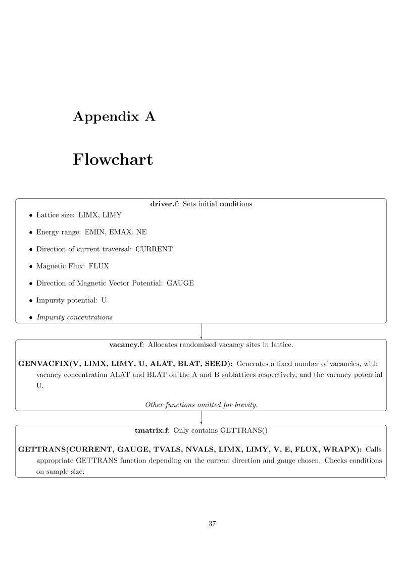
Appendix A
Flowchart
driver.f: Sets initial conditions
• Lattice size: LIMX, LIMY
• Energy range: EMIN, EMAX, NE
• Direction of current traversal: CURRENT
• Magnetic Flux: FLUX
• Direction of Magnetic Vector Potential: GAUGE
• Impurity potential: U
• Impurity concentrations
vacancy.f: Allocates randomised vacancy sites in lattice.
GENVACFIX(V, LIMX, LIMY, U, ALAT, BLAT, SEED): Generates a fixed number of vacancies, with
vacancy concentration ALAT and BLAT on the A and B sublattices respectively, and the vacancy potential
U.
Other functions omitted for brevity.
tmatrix.f: Only contains GETTRANS()
GETTRANS(CURRENT, GAUGE, TVALS, NVALS, LIMX, LIMY, V, E, FLUX, WRAPX): Calls
appropriate GETTRANS function depending on the current direction and gauge chosen. Checks conditions
on sample size.
37
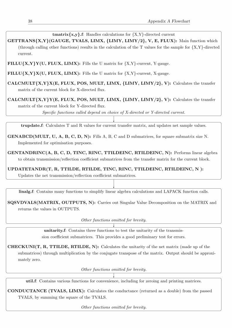
38 Appendix A Flowchart
tmatrix{x,y}.f: Handles calculations for {X,Y}-directed current
GETTRANS{X,Y}(GAUGE, TVALS, LIMX, {LIMY, LIMY/2}, V, E, FLUX): Main function which
(through calling other functions) results in the calculation of the T values for the sample for {X,Y}-directed
current.
FILLU{X,Y}Y(U, FLUX, LIMX): Fills the U matrix for {X,Y}-current, Y-gauge.
FILLU{X,Y}X(U, FLUX, LIMX): Fills the U matrix for {X,Y}-current, X-gauge.
CALCMULT{X,Y}X(E, FLUX, POS, MULT, LIMX, {LIMY, LIMY/2}, V): Calculates the transfer
matrix of the current block for X-directed flux.
CALCMULT{X,Y}Y(E, FLUX, POS, MULT, LIMX, {LIMY, LIMY/2}, V): Calculates the transfer
matrix of the current block for Y-directed flux.
Specific functions called depend on choice of X-directed or Y-directed current.
trupdate.f: Calculates T and R values for current transfer matrix, and updates net sample values.
GENABCD(MULT, U, A, B, C, D, N): Fills A, B, C and D submatrices, for square submatrix size N.
Implemented for optimisation purposes.
GENTANDRINC(A, B, C, D, TINC, RINC, TTILDEINC, RTILDEINC, N): Performs linear algebra
to obtain transmission/reflection coefficient submatrices from the transfer matrix for the current block.
UPDATETANDR(T, R, TTILDE, RTILDE, TINC, RINC, TTILDEINC, RTILDEINC, N ):
Updates the net transmission/reflection coefficient submatrices.
linalg.f: Contains many functions to simplify linear algebra calculations and LAPACK function calls.
SQSVDVALS(MATRIX, OUTPUTS, N): Carries out Singular Value Decomposition on the MATRIX and
returns the values in OUTPUTS.
Other functions omitted for brevity.
unitarity.f: Contains three functions to test the unitarity of the transmis-
sion coefficient submatrices. This provides a good preliminary test for errors.
CHECKUNI(T, R, TTILDE, RTILDE, N): Calculates the unitarity of the net matrix (made up of the
submatrices) through multiplication by the conjugate transpose of the matrix. Output should be approxi-
mately zero.
Other functions omitted for brevity.
util.f: Contains various functions for convenience, including for zeroing and printing matrices.
CONDUCTANCE (TVALS, LIMX): Calculates the conductance (returned as a double) from the passed
TVALS, by summing the square of the TVALS.
Other functions omitted for brevity.
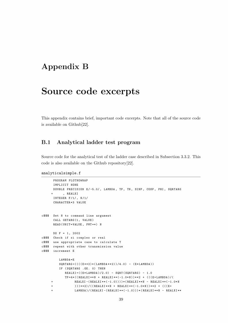
Appendix B
Source code excerpts
This appendix contains brief, important code excerpts. Note that all of the source code
is available on Github[22].
B.1 Analytical ladder test program
Source code for the analytical test of the ladder case described in Subsection 3.3.2. This
code is also available on the Github repository[22].
analyticalsimple.f
PROGRAM PLOTNOWRAP
IMPLICIT NONE
DOUBLE PRECISION E/-5.0/, LAMBDA , TP, TN, SINP , COSP , PHI , SQRTARG
+ , REALXI
INTEGER F/1/, N/1/
CHARACTER *3 VALUE
c$$$ Set N to command line argument
CALL GETARG(1, VALUE)
READ(UNIT=VALUE , FMT=*) N
DO F = 1, 2002
c$$$ Check if xi complex or real
c$$$ use appropriate case to calculate T
c$$$ repeat with other transmission value
c$$$ increment E
LAMBDA=E
SQRTARG =((((E**2)*( LAMBDA **2))/4.0) - (E*LAMBDA ))
IF (SQRTARG .GE. 0) THEN
REALXI =((E*LAMBDA )/2.0) - SQRT(SQRTARG) - 1.0
TP=4*(( REALXI **N + REALXI **( -1.0*N))**2 + (((E+LAMBDA )/(
+ REALXI -( REALXI **( -1.0))))*( REALXI **N - REALXI **( -1.0*N
+ )))**2)/(( REALXI **N + REALXI **( -1.0*N))**2 + (((E+
+ LAMBDA )/(REALXI -( REALXI **( -1.0)))*( REALXI **N - REALXI **
39
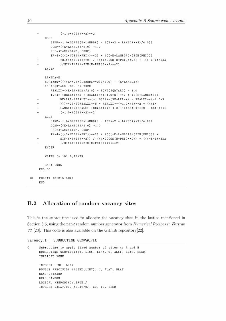
40 Appendix B Source code excerpts
+ ( -1.0*N))))**2)**2
ELSE
SINP =-1.0* SQRT((E*LAMBDA) - ((E**2 * LAMBDA **2)/4.0))
COSP =((E*LAMBDA )/2.0) -1.0
PHI=ATAN2(SINP , COSP)
TP =4*(((2* COS(N*PHI ))**2) + (((-E-LAMBDA )/( SIN(PHI)))
+ *SIN(N*PHI ))**2) / (((4*( COS(N*PHI )**2)) + (((-E-LAMBDA
+ )/SIN(PHI))*SIN(N*PHI ))**2)**2)
ENDIF
LAMBDA=E
SQRTARG =((((E**2)*( LAMBDA **2))/4.0) - (E*LAMBDA ))
IF (SQRTARG .GE. 0) THEN
REALXI =((E*LAMBDA )/2.0) - SQRT(SQRTARG) - 1.0
TN=4*(( REALXI **N + REALXI **( -1.0*N))**2 + (((E+LAMBDA )/(
+ REALXI -( REALXI **( -1.0))))*( REALXI **N - REALXI **( -1.0*N
+ )))**2)/(( REALXI **N + REALXI **( -1.0*N))**2 + (((E+
+ LAMBDA )/(REALXI -( REALXI **( -1.0)))*( REALXI **N - REALXI **
+ ( -1.0*N))))**2)**2
ELSE
SINP =-1.0* SQRT((E*LAMBDA) - ((E**2 * LAMBDA **2)/4.0))
COSP =((E*LAMBDA )/2.0) -1.0
PHI=ATAN2(SINP , COSP)
TN =4*(((2* COS(N*PHI ))**2) + ((((-E-LAMBDA )/(SIN(PHI))) *
+ SIN(N*PHI ))**2)) / ((4*(( COS(N*PHI )**2)) + (((-E-LAMBDA
+ )/SIN(PHI))*SIN(N*PHI ))**2)**2)
ENDIF
WRITE (* ,10) E,TP+TN
E=E+0.005
END DO
10 FORMAT (3ES15.5E4)
END
B.2 Allocation of random vacancy sites
This is the subroutine used to allocate the vacancy sites in the lattice mentioned in
Section 3.5, using the ran2 random number generator from Numerical Recipes in Fortran
77 [23]. This code is also available on the Github repository[22].
vacancy.f: SUBROUTINE GENVACFIX
C Subroutine to apply fixed number of sites to A and B
SUBROUTINE GENVACFIX(V, LIMX , LIMY , U, ALAT , BLAT , SEED)
IMPLICIT NONE
INTEGER LIMX , LIMY
DOUBLE PRECISION V(LIMX ,LIMY), U, ALAT , BLAT
REAL GETRAND
REAL RANDOM
LOGICAL KEEPGOING /.TRUE./
INTEGER NALAT/0/, NBLAT/0/, XC , YC , SEED
Appendix B Source code excerpts 41
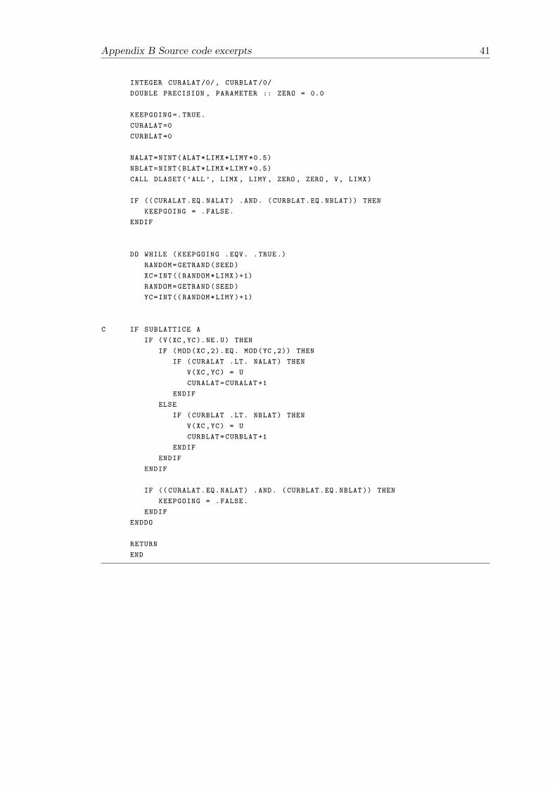
INTEGER CURALAT /0/, CURBLAT /0/
DOUBLE PRECISION , PARAMETER :: ZERO = 0.0
KEEPGOING =.TRUE.
CURALAT =0
CURBLAT =0
NALAT=NINT(ALAT*LIMX*LIMY *0.5)
NBLAT=NINT(BLAT*LIMX*LIMY *0.5)
CALL DLASET(’ALL ’, LIMX , LIMY , ZERO , ZERO , V, LIMX)
IF (( CURALAT.EQ.NALAT) .AND. (CURBLAT.EQ.NBLAT )) THEN
KEEPGOING = .FALSE.
ENDIF
DO WHILE (KEEPGOING .EQV. .TRUE.)
RANDOM=GETRAND(SEED)
XC=INT(( RANDOM*LIMX )+1)
RANDOM=GETRAND(SEED)
YC=INT(( RANDOM*LIMY )+1)
C IF SUBLATTICE A
IF (V(XC,YC).NE.U) THEN
IF (MOD(XC ,2).EQ. MOD(YC ,2)) THEN
IF (CURALAT .LT. NALAT) THEN
V(XC,YC) = U
CURALAT=CURALAT +1
ENDIF
ELSE
IF (CURBLAT .LT. NBLAT) THEN
V(XC,YC) = U
CURBLAT=CURBLAT +1
ENDIF
ENDIF
ENDIF
IF (( CURALAT.EQ.NALAT) .AND. (CURBLAT.EQ.NBLAT )) THEN
KEEPGOING = .FALSE.
ENDIF
ENDDO
RETURN
END

Bibliography
[1] D. E. Khmelnitskii. Phys. Lett., 106A:182, 1984.
[2] KS Novoselov, AK Geim, SV Morozov, D. Jiang, Y. Zhang, SV Dubonos, IV Grig-
orieva, and AA Firsov. Electric field effect in atomically thin carbon films. Science,
306(5696):666, 2004.
[3] A.K. Geim and A.H. MacDonald. Graphene: Exploring carbon flatland. Physics
Today, 60(8):35, 2007.
[4] Alexander N. Obraztsov. Chemical vapour deposition: Making graphene on a large
scale. Nat Nano, 4(4):212–213, 2009.
[5] M. I. Katsnelson, K. S. Novoselov, and A. K. Geim. Chiral tunnelling and the klein
paradox in graphene. Nat Phys, 2(9):620–625, 2006.
[6] A.K. Geim and K.S. Novoselov. The rise of graphene. Nature materials, 6(3):183–
191, 2007.
[7] K. Jensen, K. Kim, and A. Zettl. An atomic-resolution nanomechanical mass sensor.
Nat Nano, 3(9):533–537, 2008.
[8] Fengnian Xia, Thomas Mueller, Yu-ming Lin, Alberto Valdes-Garcia, and Phaedon
Avouris. Ultrafast graphene photodetector. Nat Nano, 4(12):839–843, 2009.
[9] Yanqing Wu, Yuming Lin, Ageeth A. Bol, Keith A. Jenkins, Fengnian Xia, Da-
mon B. Farmer, Yu Zhu, and Phaedon Avouris. High-frequency, scaled graphene
transistors on diamond-like carbon. Nature, 472(7341):74–78, 2011.
[10] Fengnian Xia, Damon B. Farmer, Yuming Lin, and Phaedon Avouris. Graphene
field-effect transistors with high on/off current ratio and large transport band gap
at room temperature. Nano Letters, 10(2):715–718, 2010. PMID: 20092332.
[11] A. Neto, F. Guinea, N. Peres, et al. The electronic properties of graphene. Reviews
of Modern Physics, 81(1):109–162, 2009.
[12] R. S. Deacon, K.-C. Chuang, R. J. Nicholas, K. S. Novoselov, and A. K. Geim.
Cyclotron resonance study of the electron and hole velocity in graphene monolayers.
Phys. Rev. B, 76:081406, Aug 2007.
43
44 BIBLIOGRAPHY
[13] Mikhail I. Katsnelson. Graphene: Carbon in Two Dimensions. Cambridge Univer-
sity Press, Cambridge, UK, 1992.
[14] Andrea F. Young and Philip Kim. Quantum interference and klein tunnelling in
graphene heterojunctions. Nat Phys, 5(3):222–226, 2009.
[15] Yoseph Imry and Rolf Landauer. Conductance viewed as transmission. Reviews of
Modern Physics, 71(2):306–312, 1999.
[16] F Miao, S Wijeratne, Y Zhang, U C Coskun, W Bao, and C N Lau. Phase-
coherent transport in graphene quantum billiards. Science (New York, N.Y.),
317(5844):1530–3, September 2007.
[17] D. R. Yennie. Integral quantum hall effect for nonspecialists. Rev. Mod. Phys.,
59:781–824, Jul 1987.
[18] H. Paul. Introduction to Quantum Theory, pages 156–157. Cambridge University
Press, Cambridge, UK, 2008.
[19] S V Morozov, K S Novoselov, and A K Geim. Electron transport in graphene.
Physics-Uspekhi, 51(7):744, 2008.
[20] V. F. Gantmakher. Electrons and Disorder in Solids. Oxford University Press,
Oxford, UK, 2005.
[21] Patrick A. Lee and T. V. Ramakrishnan. Disordered electronic systems. Rev. Mod.
Phys., 57:287–337, Apr 1985.
[22] James McMurray. Doping-effects-in-graphene repository, April 2013.
[23] William H. Press, Saul A. Teukolsky, William T. Vetterling, and Brian P. Flannery.
Numerical Recipes in Fortran 77, pages 272–273. Cambridge University Press,
Cambridge, UK, 1992.
[24] B.I. Halperin et al. Quantised hall conductance, current carrying edge states and
the existence of extended states in a two-dimensional disordered potential. Phys
Rev B, 25:2185–2190, 1982.
[25] R. B. Laughlin. Phys. Rev. Lett., 52:2304, 1984.
[26] Steven E Martins, Freddie Withers, Marc Dubois, Monica F Craciun, and Saverio
Russo. Tuning the transport gap of functionalized graphene via electron beam
irradiation. New Journal of Physics, 15(3):033024, 2013.