Embed Size (px)
DESCRIPTION
We present here theoretical study of the electronic bands structure E (d1) of InAs (d1=25 Å)/GaSb (d2=25 Å) type II superlattice at 4.2 K performed in the envelope function formalism. We study the effect of d1 and the offset , between heavy holes bands edges of InAs and GaSb, on the band gap Eg (), at the center of the first Brillouin zone, and the semiconductor-to-semimetal transition. Eg (, T) decreases from 288.7 meV at 4.2 K to 230 meV at 300K. In the investigated temperature range, the cut-off wavelength 4.3 m ≤ c ≤ 5.4 m situates this sample as mid-wavelength infrared detector (MWIR). Our results are in good agreement with the experimental data realized by C. Cervera et al.
Citation preview
A. Boutramine et al. Int. Journal of Engineering Research and Application www.ijera.com
ISSN : 2248-9622, Vol. 4, Issue 12( Part 6), December 2014, pp.132-135
www.ijera.com 132 | P a g e
Electronic bands structure and gap in mid-infrared detector
InAs/GaSb type II nanostructure superlattice
A. Boutramine, A. Nafidi, D. Barkissy, A. Hannour, M. Massaq, H. Chaib Laboratory of Condensed Matter Physics and Nanomaterials for Renewable Energy University Ibn Zohr, 80000
Agadir, Morocco.
ABSTRACT We present here theoretical study of the electronic bands structure E (d1) of InAs (d1=25 Å)/GaSb (d2=25 Å) type
II superlattice at 4.2 K performed in the envelope function formalism. We study the effect of d1 and the offset ,
between heavy holes bands edges of InAs and GaSb, on the band gap Eg (), at the center of the first Brillouin
zone, and the semiconductor-to-semimetal transition. Eg (, T) decreases from 288.7 meV at 4.2 K to 230 meV
at 300K. In the investigated temperature range, the cut-off wavelength 4.3 m ≤ c ≤ 5.4 m situates this sample
as mid-wavelength infrared detector (MWIR). Our results are in good agreement with the experimental data
realized by C. Cervera et al.
Keywords - Bands structure, envelope function formalism, InAs/GaSb type II superlattice, mid-infrared
detector, semiconductor-semimetal transition.
I. INTRODUCTION
The idea of the type II InAs/GaSb superlattice
(T2SL) was firstly suggested by Sai-Halasz and
coworkers in 1977 [1]. The application of such (SL),
only after several years, was proposed as an infrared
sensing material by Smith and Mailhoit in 1987 [2].
Since then, the (T2SL) have made significant
progress and attracted increasing interest for mid (3–
5m) [3] and long wavelength infrared region (8–
12m) [4].
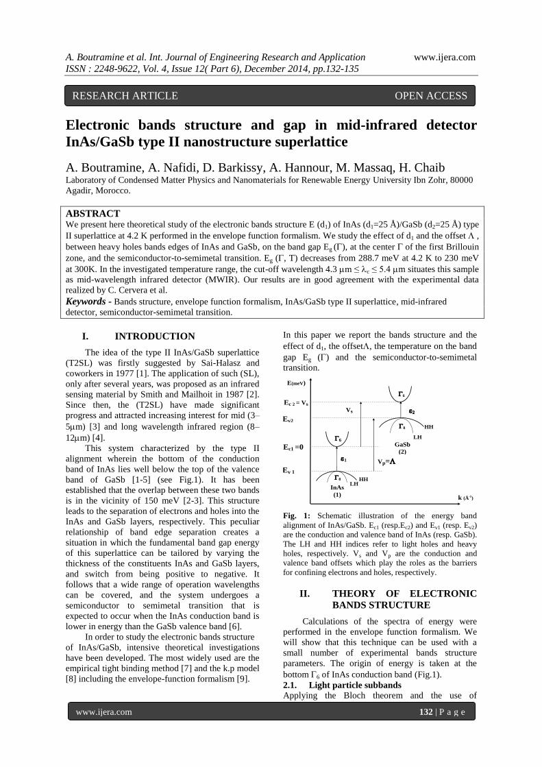
This system characterized by the type II
alignment wherein the bottom of the conduction
band of InAs lies well below the top of the valence
band of GaSb [1-5] (see Fig.1). It has been
established that the overlap between these two bands
is in the vicinity of 150 meV [2-3]. This structure
leads to the separation of electrons and holes into the
InAs and GaSb layers, respectively. This peculiar
relationship of band edge separation creates a
situation in which the fundamental band gap energy
of this superlattice can be tailored by varying the
thickness of the constituents InAs and GaSb layers,
and switch from being positive to negative. It
follows that a wide range of operation wavelengths
can be covered, and the system undergoes a
semiconductor to semimetal transition that is
expected to occur when the InAs conduction band is
lower in energy than the GaSb valence band [6].
In order to study the electronic bands structure
of InAs/GaSb, intensive theoretical investigations
have been developed. The most widely used are the
empirical tight binding method [7] and the k.p model
[8] including the envelope-function formalism [9].
In this paper we report the bands structure and the
effect of d1, the offset, the temperature on the band
gap Eg () and the semiconductor-to-semimetal
transition.
Vp=
InAs
(1)
8
HH
6
k (Å-1)
E(meV)
LH
Ec1 =0
Ev 1
GaSb
(2)
6
8
Ec 2 = Vs
HH
LH
Ev2
Vs
1
Fig. 1: Schematic illustration of the energy band
alignment of InAs/GaSb. Ec1 (resp.Ec2) and Ev1 (resp. Ev2)
are the conduction and valence band of InAs (resp. GaSb).
The LH and HH indices refer to light holes and heavy
holes, respectively. Vs and Vp are the conduction and
valence band offsets which play the roles as the barriers
for confining electrons and holes, respectively.
II. THEORY OF ELECTRONIC
BANDS STRUCTURE
Calculations of the spectra of energy were
performed in the envelope function formalism. We
will show that this technique can be used with a
small number of experimental bands structure
parameters. The origin of energy is taken at the
bottom 6 of InAs conduction band (Fig.1).
2.1. Light particle subbands
Applying the Bloch theorem and the use of
RESEARCH ARTICLE OPEN ACCESS

A. Boutramine et al. Int. Journal of Engineering Research and Application www.ijera.com
ISSN : 2248-9622, Vol. 4, Issue 12( Part 6), December 2014, pp.132-135
www.ijera.com 133 | P a g e
appropriate matching conditions at the interface,
leads to the general dispersion relation of the (SL)
light particle (electron and light hole) subbands
given by the expression [9]: 2
p
z 1 1 2 2 1 1 2 2
1 2
k1 1 1cos(k d) cos(k d )cos(k d ) ( ) (r 2) sin(k d )sin(k d )
2 4k k r
(1)
Here, k1 and k2 are the wave vectors along the z axis.
The two-dimensional wave Vector kp(kx,ky)
describes the motion of particles perpendicularly to
kz. d1 and d2 refer to the thickness of InAs and GaSb
layers, respectively. Finally is given by:
1 1 2
2 2 2
k k E-ε -Λ= r=
k k E-ε (2)
At given energy, the two–band Kane model [10]
gives the wave vector (2 2
i pk +k ) in each host material
by:
2 2 2 2
1 p 1
2 2 2 2
2 p 2
2P h (k +k )=(E-ε )E :InAs
32
P h (k +k )=(E-ε -Λ)(E-Λ):GaSb3
(3)
1and 2 are the interaction band gaps of InAs and
GaSb, respectively. We use the valence band offset
=570 meV determined by far-infrared absorption
in a magnetic field for different hydrostatic pressures
[11]. P is the Kane matrix element which is taken to
be 1.36.106 J/kg for InAs and 1.41.10
6 J/kg for GaSb
[12]. At given energy E, a (SL) state of wave vector
kz exists if the right-hand-side of (1) lies in the range
(-1, +1) that implies −/d≤ kz ≤ /d in the first
Brillouin zone.
2.2. Heavy hole subbands
The (SL) heavy hole subbands are obtained
from the same equation (1) with: *1
2 2 HH
1 p 2*2
2 2 HH
2 p 2
2mk +k = (E-Λ) :InAs
h2m
k +k = E :GaSbh
(4)
*2
1 1 HH
*12 2 HH
k k mr
k k m (5)
Where m
*1HH =0.41m0 and m
*2HH =0.44m0 are the
heavy hole masses in InAs and GaSb, respectively.
These experimental values are determined
respectively by F. Matossi et al in p-type InAs [13],
and A. Filion by magneto-photoconductivity in
GaSb at 4.2 K [14].
III. RESULTS AND DISCUSSIONS
When d1 increase, Fig.2 shows that the energy
of electrons E1, in the InAs layer, decreases. While
the energy of heavy holes HH1, in GaSb, increases in
agreement with the prevision of [15]. The crossover
of E1 and HH1 occurs when d1(InAs) reaches a
critical value d1c=74 Å, corresponding to the energy
Ec=558 meV. Then, the (T2SL) achieves a
semiconductor-to-semimetal transition. After, E1 lie
down HH1 and Eg(becomes negative assuming a
semimetallic conductivity. In this case, the electrons
flood from the GaSb valence band to the InAs
conduction band minimum.
InAs/GaSb
25 Å/25 Å, T = 4.2 K
= 570 meV
10 20 30 40 50 60 70 80
10 20 30 40 50 60 70 80
0
200
400
600
800
1000
0
200
400
600
800
1000
T'c
HHkz=/d1
HHkz=01
hkz=/d1h
kz=01
E0<kz</d2
Ekz=/d1
Ekz=01
E (
meV
)
d1 (Å)
Eg= 288.7
Fig. 2: Energy position and width of the conduction (Ei),
heavy-hole (HHi), and light-hole (hi) subbands calculated
at 4.2 K, in the first Brillion zone, as a function of the
d1(InAs) layer thickness.
In the Fig.3, when the offset increases, the
band gap Eg () increases to a maximum near 600
meV at =-44 meV. After it decreases to zero at the
transition semiconductor-to-semimetal conductivity,
and becomes negative accusing a semimetallic
conduction after c =990 meV at T=4.2 K. Our
chosen value of 570 meV is indicated by a vertical
dashed line. This offset is closed to 500 meV used
-300 0 300 600 900 1200
-300 0 300 600 900 1200
0
200
400
600
0
200
400
600
Eg(
) (m
eV)
(meV)
InAs/GaSb
T=4.2 K
25Å / 25 Å
c
Fig. 3: The band gap Eg() at , as function the offset at
4.2 K, for the investigated InAs/GaSb (SL) with
d1=d2=25Å.
by L. L. Li et al [15] for a sample with d1=23.5 Å
and d2=24 Å.

A. Boutramine et al. Int. Journal of Engineering Research and Application www.ijera.com
ISSN : 2248-9622, Vol. 4, Issue 12( Part 6), December 2014, pp.132-135
www.ijera.com 134 | P a g e
Fig.4 shows that when d1 increases Eg ()
decreases, go to zero at the transition point T’c, and
becomes negative with a semimetal conductivity.
The cut-off wavelength |c| diverge at T’c with
d1c=74 Ǻ. This band gap variation can be understood
using this simple model; the InAs layer acts as a
quantum well confining the conduction electrons.
It’s well known that the energy level of a particle is
closely inversely proportional to its effective mass
InAs/GaSb
d1=d
2=25 Å
4.2K
= 570 meV
20 40 60 80 100
20 40 60 80 100
0
200
400
600
d1 (Å)
Eg(
)(m
eV
)
d1c
0
100
200
300
|
c|(
m)
Fig.4: Band gap energy Eg () and the cut-off wavelength
|c| as a function of InAs layer width d1 at 4.2K.
and the square of the well width. When the InAs
well width increases, the energy level of the
electrons miniband in the InAs layer decreases,
leading to a decrease in the band gap. On another
hand, the GaSb layer is envisioned as a well for
holes. Because of the bigger GaSb valence band
effective mass, the dependence of the energy on the
well width becomes much smaller. This behavior
can also be explained by the “model-solid theory” of
Van de Walle and Martin [16], which describes the
shift in position of the conduction and valence band
when the volume of the crystal changes (id d1 and/or
d2).
Significant research and number of empirical
models has been developed to describe the
temperature-dependent behavior of band gap on
various semiconductors. Among them, the Varshni
model [17] suggests that in semiconductors the
temperature dependence of band gap derives partly
from the lattice expansion of the crystal and partly
from the electron-phonon interaction. Using the value of ε1 and ε2 at different
temperatures between 4.2 K and 300 K, we get the
temperature dependence of the band gap Eg( in
Fig.5 which can be described quite well by the
empirical Varshni form [17]. 2
g g
TE (T)=E (T=0)-α (meV)
T+β (6)
The zero temperature extrapolated energy gap Eg
(T=0), and the coefficients and for our (SL) are
listed in Tab.1.
Tab.1: Fit parameters for temperature dependence of
superlattice band gap.
The both experimental results and our
calculated band-gap (and the cut-off wavelength) as
function of temperature are shown in Fig.5. This
shift of band gap arises mainly from the decreasing
of the potential seen by the electrons in the material
due to the increase of the interatomic spacing. The
detection cut-off wavelength was calculated
Our calculations:=570 meV
Our calculation :=650 meV
Our calculation ofc for C. Cervera et al [18].
Our calculations:=570 meV
Our calculation :=650 meV
C. Cervera and al [18]
0 50 100 150 200 250 300
240
280
0 50 100 150 200 250 300
InAs/GaSb
25Å / 25 Å
Eg(
)(m
eV
)
T(K) T(K)
0 50 100 150 200 250 300
0 50 100 150 200 250 300
4
5
6
InAs/GaSb
25Å / 25 Å c(
m)
Fig.5: Temperature dependence of the band gap Eg (Left panel). The right panel shows the Cut-off wavelength c, at the
center -point of the first Brillion zone.
Eg(0)(meV) (meV/K) (K)
InAs/GaSb[18]
277 0.34 254
InAs/GaSb
(=570meV)
288.8 0,36 241
InAs/GaSb
(=650meV)
279.2 0.37 258

A. Boutramine et al. Int. Journal of Engineering Research and Application www.ijera.com
ISSN : 2248-9622, Vol. 4, Issue 12( Part 6), December 2014, pp.132-135
www.ijera.com 135 | P a g e
using the expression:
cg
( m)1240
E (meV) (7)
We note that the offset of the sample
characterized by Cervera et al. is not indicated in
[18]. According to our calculations the offset
=650 meV give a good agreement of our
calculations with the experimental data in [18]. For
=570 meV, the fundamental gap energy decreases
from 288.7 meV at 4.2 K to 230 meV at 300K. In
the investigated temperature range, the cut-off
wavelength 4.3m ≤ c ≤ 5.4m situates this
sample as a mid-infrared detector (MWIR).
IV. CONCLUSION
Our calculations of the electronic bands
structure E(d1) at 4.2K had shown that when d1 and
the offset increases, Eg decreases to zero with a
transition semiconductor to semimetal,
respectively, for d1c=74 Å and c =990 meV. When
the temperature increases, the Eg(, T) decreases
from 288.7 meV at 4.2 K to 230 meV at 300K
corresponding to the cut-off wavelength 4.3m ≤ c
≤5.4m which situates this sample as mid-
wavelength infrared detector (MWIR). Our results
are in good agreement with the experimental data
realized by C.Cervera, et al. for an offset =650
meV. Note that we had observed a semiconductor
type n conduction mechanism in a narrow gap,
two-dimensional and far-infrared detector
HgTe/CdTe type III superlattice [19].
REFERENCES [1] G. A. Sai-Halasz, R. Tsu, and L. Esak, A
new semiconductor superlattice Appl. Phys.
Lett. 30, 1977, 651-653.
[2] D. L. Smith and C. Mailhiot, Proposal for
strained type II superlattice, infrared
detectors, J.Appl.Phys.62, 1987, 2545-2548.
[3] A. Rogalski, Material considerations for
third generation infrared photon detectors,
Infrared Phys.Technol, 50, 2007, 240-252.
[4] H. Mohseni, M. Razeghi, Long-Wavelength
Type-II Photodiodes operating at room
temperature, IEEE Photon. Technol. Lett.
13, 2001, 517-519.
[5] G. A. Sai-Halasz, L.L.Chang, J.M.Walter,
C.A. Chang, and L. Esaki, Optical
absorption of In1-x GaxAs-GaSb1-yAsy
superlattices, Solide State Commun. 27,
1978, 935-939.
[6] M. Altarelli, Electronic structure and
semiconductor-semimetal transition in InAs-
Gasb superlattices , Phys. Rev. B 28, 1983,
842-845.
[7] Wei Y and M.Razeghi, Modeling Type II
InAs/GaSb superlattices using empirical
tight-binding method: new aspects, Proc. of
SPIE Vol. 5359, 2004, 301-308.
[8] Mohseni H, Lit vinov V I and M. Razeghi,
Interface-induced suppression of the Auger
recombination in type-II InAs/GaSb
superlattices, Phys. Rev.B, 58, 1998,15378-
15380.
[9] G. Bastard, Superlattice band structure in
the envelope-function approximation,
Phys.Rev. B, Vol 24, 1981, 5693-5697; A.
Nafidi, et al, in Book of Abstracts of the
International Conference on Theoretical
Physics (HT 2002), Paris, France, 22–27
July 2002, 274–275.
[10] E.O. Kane, Band structure of indium
antimonid, J. Phys. Chem. Solids 1(4), 1957
,249–261.
[11] L. M. Claessen,J. C. Maan, M. Altarelli, and
P. Wyder, Pressure Dependence of Band
Offsets in an InAs-GaSb Superlattice, Appl.
Phys. Lett. 57, 1986, 2556-2559.
[12] Jérôme faist, Quantum cascade lasers, 1st
edn. ISBN 978-0-19-852824-1 (Oxford
university press), 2013, p. 28
[13] F. Matossi and F. Stern, Temperature
Dependence of Optical Absorption in p-
Type Indium Arsenide, Phys.Rev, B, Vol
111, 1958, 472-475.
[14] Filion and E. Fortin, Photoconductivity
associated with landau structure in GaSb,
Phys. Rev. B 8, 1973, 3852-3860.
[15] L. L. Li,1 W. Xu, J. Zhang, and Y. L. Shi ,
Midinfrared absorption by InAs/GaSb type-
II superlattices, J. Appl. Phys. 105, 2009,
013115.
[16] C. G. Van de Walle, Band lineups and
deformation potentials in the model-solid
theory, Phys. Rev. B 39, 1989.
[17] Y.P.Varshni, Temperature dependence of
the energy gap in semiconductors, Physica
34, 1967, 149-154.
[18] C. Cervera, J. B. Rodriguez, J. P. Perez, H.
Aït-Kaci, R. Chaghi, L. Konczewicz, S.
Contreras, and P. Christol, Unambiguous
determination of carrier concentration and
mobility for InAs/GaSb superlattice
photodiode optimization, J. Appl. Phys.106,
2009, 033709.
[19] M. Braigue, A. Nafidi, et al, Correlation
Between Band Structure and Magneto-
Transport Properties in HgTe/CdTe Two
Dimensional Far-Infrared Detector
Superlattice, Journal of Low Temperature
Physics, Volume 171, Issue 5-6, Springer,
2013,808-8.