Embed Size (px)
Citation preview
) LALRT 00-12
Kovember 2000
Electronic Front-End for LHCb Electromagnetic
and Hadronic Calorimeters
Christophe Beigbeder
Laboratoire de IAccelerateur Lineaire 2P3-CKRS et UuiVfgtngtittgt ltifgt Paris-Slid DP 34 F-91898 Onay Cpltlex
Talk giveamp flt tIl( ]Xth ]ampt(nultitmal Cfmj(1fmf( fm Calmim(t111 in Panicle Physics 9-1 October 2000 Annccy France
Institut NationalUER de Physique Nucleairede
et de Physique des ParticuleslUniversite Paris-Sud
BP 34 - Batiment 200 - 91898 ORSAY CEDEX
LALRTOO-1 2 November 2000
ELECTRONIC FRONT-END FOR LHCb ELECTROMAGNETIC A N D HADRONIC CALORIMETERS
Christophe Beigbeder Labo ratoire de I Accelb-ateur Lineaire
IN2P3-CNRS et Universi te de Paris-Sud BP 34 91898 Orsay Cedex - France
ABSTRACT
T he electronic front-end or the LHCb electromagnetic and hadronic calorimeshyters will be described It con lsts of a 9U 32 channel board each channel including shaper-integrator 12 bit ADC and lookup tables allowing to code the transverse energy information both for readout and for the Level 0 trigger The readout information is stored in a fixed latency followed by a derandomshyizer The trigger information is processed fur ther on the board by FPG A performing channel addi tion and comparison to ext ract the highest transverse energy local cluster for further processing The lSystem is fully synchronous and allows to ext ract candidates for calorimetric tr igger at every 40 MHz clock cycle The operation and characteristics (noise linearity etc) of a prototype board will be described
1 Introduction
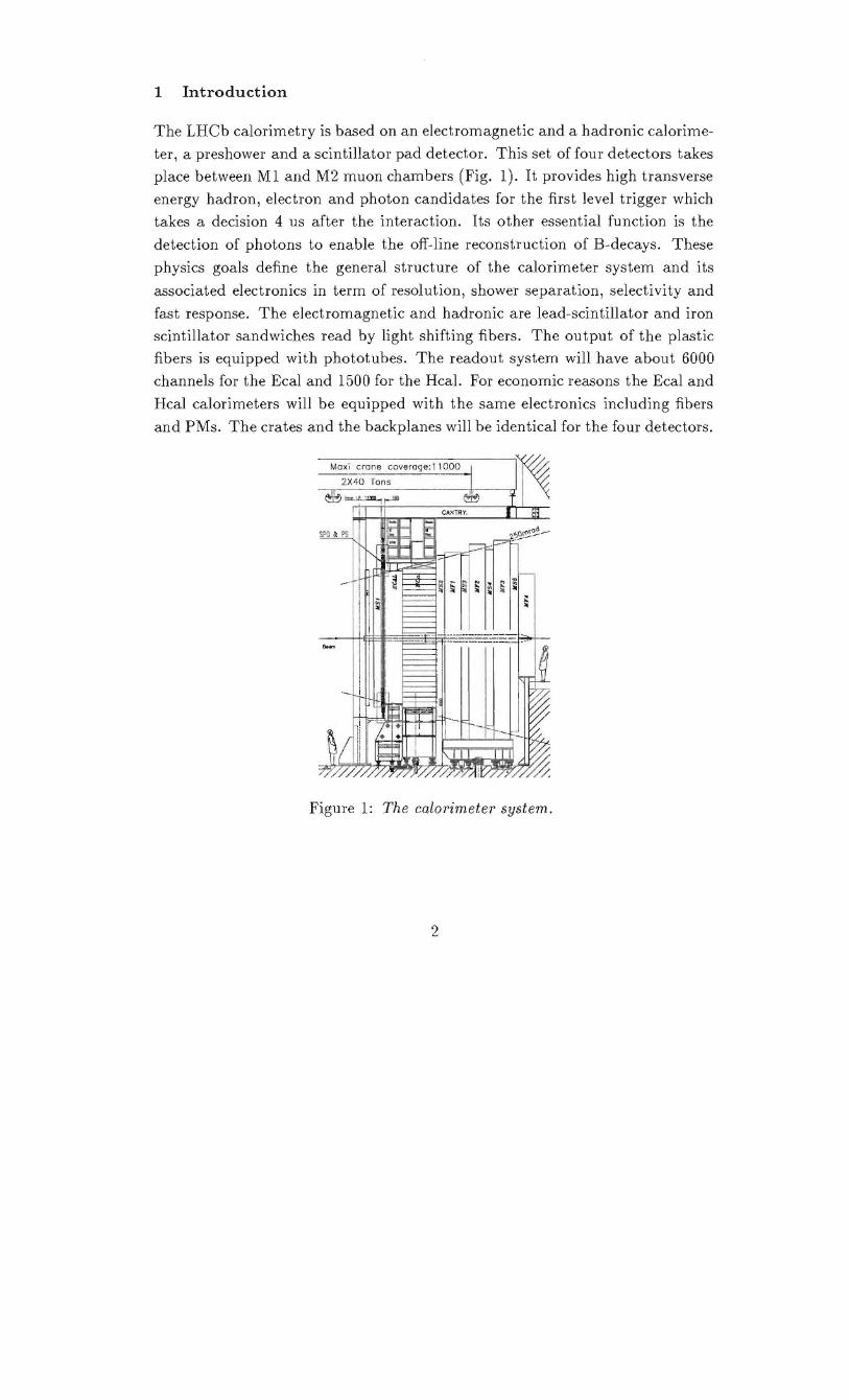
The LHCb calorimetry is based on an electromagnetic and a hadronic calorimeshy
ter a preshower and a scintillator pad detector This set of four detectors takes
place between M1 and M2 muon chambers (Fig 1) It provides high transverse
energy hadron electron and photon candidates for the first level trigger which
takes a decision 4 us after the interaction Its other essential function is the
detection of photons to enable the off-line reconstruction of B-decays These
physics goals define the general structure of the calorimeter system and its
associated electronics in term of resolution shower separation selectivity and
fast response The electromagnetic and hadronic are lead-scintillator and iron
scintillator sandwiches read by light shifting fibers The output of the plastic
fibers is equipped with phototubes The readout system will have about 6000
channels for the Ecal and 1500 for the Heal For economic reasons the Ecal and
Heal calorimeters will be equipped with the same electronics including fibers
and PMs The crates and the backplanes will be identical for the four detectors
2X+O Tons
~~r
Figure 1 The calorimeter system
2
2 Requirements
The main requirement for LHCb electronics is the pile-up rejection To ensure
a satisfactory independence of successive samplings it makes use of fast fibers
fast PMs and shaping Shaped signal has to be sampled at 40 MHz on 12 bits to
cover the resolu tion over the full dynamic range of the two calorimeters ( 50 MeV
to 200 GeV) The data are transcoded within LUTs into energy over 8 bits for
trigger data and 12 bits for readout data The latter has to be buffered during
the first level (LO) latency of 32 JLsec derandomized and then rebuffered for
the second level (L 1) latency of 256 JLsec 1) After the L 1 trigger an extended
zero suppression needs to be performed before sending the formatted event to
the DAQ There are also trigger elements sitting in the front-end crate The
first stages concern the search for local maxima inside groups of 512 channels
with a validation by the Preshower and Pad Chamber data
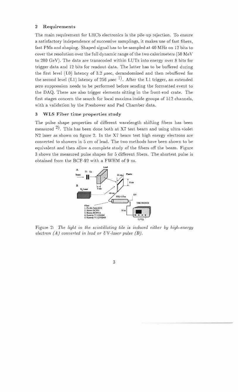
3 WLS Fiber time properties study
The pulse shape properties of different wavelength shifting fibers has been
measured 2) This has been done both at X7 test beam and using ultra-violet
N2 laser as shown on figure 2 In the X7 beam test high energy electrons are
converted to showers in 5 cm of lead The two methods have been shown to be
equivalent and then allow a complete study of the fibers off the beam Figure
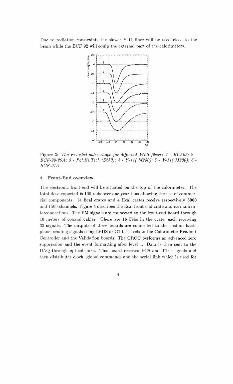
3 shows the measured pulse shapes for 5 different fibers The shortest pulse is
obtained from the BCF-92 with a FVHM of 9 ns
Fiber --shyJ PoilliTechS250 2 Bicron BCF92 J BicroD BCF91A 4 K1lnrty Yll(200)M S Kuruwy Yll(2S0)MS
Figure 2 The light in th e scintillating tile IS induced either by high-energy electron (A) converted in lead or UV-Iaser pulse (B)
3
4
Due to radiat ion constraints the slower Y-II fiber will be used close to the
beam while the BCF 92 will equip the external part of the calorimeters
u si J i u ~ E lt3 middot05I l
-1
middot15
middot2
-25
-3
~middot35
-4
J
2
3
4
5
-20 -10 0 10 20 30 40 ns
Figure 3 Th e recorded pulse shape for different WLS fibers I - BCF92 2 shyBCF-99-29A - 3 - Pol Hi Tech (S250)- 4 - Y-II ( M250)- 5 - Y-ll ( M200) 6 shyBCF-91A
Front-End over view
The electronic front-end will be situated on the top of the calorimeter The
total dose expected js 100 rads over one year thus allowing the use of commershy
cial components 14 Ecal crates and 4 Hcal cra tes receive respectively 6000
and 1500 channels Figure 4 describes the Ecal front-end cra te and its main inshy
terconnections The P M signals are connected to the front-end board through
10 meters of coaxial cables There are 16 Febs in the crate each receiving
32 signals The outputs of these boards are connected to the custom backshyplane sending signals using LVDS or GTL+ levels to the Calorimeter Readout
Controller and the Validation boa rds The CROC performs an advanced zero
suppres ion and the event formatting after level L Data is then sent to the
DAQ through optical links This board receives ECS and TTC signals and
then distributes clock global commands and the serial link which is used for
4
__
5
To T~ Selection craie optical
--~ro DAQ opticat
----4- From TTC OptiCal
~ECS eJectricai
loading the hardware over the whole crate From its 32 signals and using also
neighboring cells each FEB computes in pipeline mode the maximum of the
32 sums over every 2x2 cell area This maximum is sent to the Trigger Valishy
dation Board assuming 8 Febs for one Validation The Preshower and the Pad
Chamber validate the Ecal candidate Ecal candidates validates Heal ones
The output is sent to selection crate via optical links to get the highest (and
second highest) of the candidates this being done for each type of particle
On henJP Q tluCalorimeter
Heal eandidlte P resh ower and SPD inform ati ol
-6I)i)I) +1500 cJttuurls in 14 Ect1 and 4 Hw Crtlks
Delpoundctor
10 meter cable PM
Figure 4 The front-end crate
The Front-End board
Figure 5 shows the block diagram of the 32 channel front-end board The latter
is a 9U board using VME mechanics but without the VME bus The access
to the board for initialization and monitoring will be performed thanks to a
serial bus which has still to be defined The main data path inside the board
starts with the four 8-channel coaxial input connectors The signal goes into
the cable compensation a pole zero network compensating for a 10 - 20 nsec
signal tail before entering the analog chip These front-end elements will be
described in the next chapter After a 12bit ADC conversion data undergoes
a subtraction of the smallest of the two previous samples This subtraction
is intended to reduce the high bandwidth noise of the integrator and the two
5
samples are used to decrease the probability that a signal IS present In the
sample which is subtracted
Stl) - ~D INOS to V4 rti l n~8 tgt
Sb OTLo- frOll) a ido oe l bogt r
Igt
Pr-ont Pannel Conrloc tor
III cll ne l lcCfllt PtU ]
Figure 5 Synopsis of the front-end board
This operation is performed at 40 MHz and has been integrated in a big
FPGA Then data is converted into energy within two LUTs one for the trigger
which outputs 8 bits for transverse energy the other for the readout data which
outputs 12 bit words in a pseudo floating format allowing gain compensation
The latter data is then sent to the LO latency pipeline LO derandomizer and
L1 latency buffer After L1 trigger data is tagged with the bunch crossing
ID serialized and then sent across the backplane using LVDS levels towards
the Calorimeter crate controller At the right top of the board is the trigger
part Looking for the local maximum over the 32 channels needs to receive an
extra row and an extra column of cells and therefore send it to the neighbors
This is performed via both point to point GTL+ link on the backplane and
Cat5 cables at 280 MHz to the neighbor crate after serialization Trigger data
is first added in squares of 4 cells still preserving the original granulari ty then
compared looking for the local maximum on the board The latter is sent with
its address towards the Trigger Validation Board Beside those data paths
some utility functions have been implemented To correct for variable time
6
6
delay in PM and spread time in fibers one can adjust the sampling time on the
plateau of the analog signal for every channels thanks to programmable delay
chips with a precision of 1 ns It covers a range of 12 ns thus allowing to align
all the channels in the same bunc~ crossing A functional analog calibration has
also been implemented to check the complete readout chain This has already
been useful during the test beam operations Another important element is the
use of test procedure generated inside the PGA dedicated to the subtraction
and which can output special pattern and allows to test and debug the complete
trigger chain
The Front-End elements
The purpose of those elements is to shape the PM pulses in less than 25 ns to
avoid electronics pile-up The characteristics aimed for are the following
bull At the input the PM maximum current is 20 rnA over 25 ohms
bull At the output the ADC input dynamic range is 1 V under 250 ohms
bull The residue after 25 ns should be smaller than 1
bull The sampling area should cover +- 2 nsec with a 1 precision
bull The RMS noise should be lt 1 ADC count (250uV)
To fulfil the above requirements two problems have to be solved The
first one concerns the PM signal If one looks at Fig 6 which shows an PM
signal the PM output current has a fast rise time but a slow decay that goes
over at least the two consecutive samples at 40 MHz
~
~ E ~
~ ( Z
60 ns
Figure 6 PM output pulse with and without the clip
7
O~~-~~~~~--~~=---n
(J2 ~ -- --------+ -- shy
(J4
(JS --- bull-------------bull -----------------t
(JB
1
1 __ l
-- --bull-- -l-middot--middotmiddot----middot----middot middot--middotmiddot------ middot----middot--middot----middot--L -- -- ------ -shy -- --
-20 o 20 40
Normal and Clipped ( 5 + 5 ns 23 Ohms) Signal
It thus needs to be pulled to zero after 10 ns to ensure the zero pile-up requireshy
ments The remaining area is on the order of 60 of the original one To
perform this cut on the signal) the clipping circuit shown on Fig 7 will be used
It consists in a short 5 nsec cable located at the output of the PM base The
signal is sent towards a variable network which will send back an inverted part
of it
Cf=4pF
1---+ ADC
8uff~ lnl1JlBlor
1 BiCMOS O811m Integrated Circuit
4 Channels per chip
Figure 7 Front-end Electronics
As both the source and reflected signals are) on average) negative exponential)
their superposition gives an almost zero signal) as shown in blue line on fig
3 Now that the input signal has been shaped) we have to measure the energy
deposited in the calorimeter The corresponding information is the area of the
PM signal The best way to measure it without deteriorating too much the
stati~tic fluctuation is to integrate this signal in a capacitor (Cf) as shown in
figure 7 The difficulty then becomes to empty this capacitor Two ways are
possible
bull Use a switch mounted in parallel but this system induces a dead
time when the capacitor is being emptied) which implies the use of two
integrators in parallel and a multiplexor But due to the inevitable inshy
jection of charge from the svvitches) pedestals are generated which can be
the sources of offset shifts at the 1 level
8
7
bull Subtract in a linear way the signal to itself thanks to a specific
configuration The latter is the chosen solution 1 he configuration
appears in the middle of Fig 5 The input signal is diverted delayed
by 25 ns then subtracted to itself thanks to the differential buffer The
latter also has in charge the division of the input current to adapt it to
the small value of Cf This sol ution is the one already proposed in the
LlICb technical proposal
The buffer and the integrator inside the dashed line of the fig5 have been
integrated in a 08 urn BICMOS Asic It houses 4 channels in a 44 pin plastic
package The performances of the chip are summarized in table 1
Table l first results from the test bench
Simulation Results Current Test Bench ResuJts
Dynamic Range 14 V ltcent=gt 14 V Non Linearity 05 ltcent=gt lt 1 over the whole uynam ic range Resid ue after 25 ns lt 05 ltcent=gt lt 1 (undershoot 3) RMS Noise after ~iUbtraction 1 ADC count ltcent=gt 1 1 ADC Count Power Con umption 40m W j Channel centgt 38 m W Channel Open- Loop Gain 60 dB ltcent=gt - 60 dB gm (Input PMOS) = 34 mAV gm (Input PMOS) = 18 mAjV Fall Time 3 us lt==gt 2 us Rise Time 25 ns lt==gt 5 ns Input Impedance 190 n centgt 270 n
The functionaHty of the chip is sati~factory and 1i is mounted on a prototype
of the front-end board used in test beam The results show a good adeq ua tion
between simulation and real circuii except for the gm of the input transistor
This is due to simulation models and also explains the mi matches with the
measurement in the rise time and the input impedance of the integrator
The prototype Front-End Board
Fig 8 offers a picture of the board On the left side one can see the 2 x 8 channel input connectors followed by the PM and cable compensation networks and
the delay lines The four 4 channel analog chips are followed by half the ADCs
9
8
and the LUTs All the big FPGAs (lOK50 and 6K16) are on the other side of
the board together with the other half of the ADCs
Figure 8 Top layer of the prototype FEB
Test Beam Results
The width of the signal at the output of the chip (figure 9) is larger than on
test bench because of the fiber decay time and PM risetime 0r
ll E 08laquo 0 1 06 lti e l5 04 z
02
o
L I
-- _ i -60 -40 middot20 o 20 40
no Integrated Signal
Figure 9 Output signal after integration
Nevertheless the shape at the output of the integrator matches the requirements with a flat top within 1 for +-2 nsec and a small residue after and before
25 ns
10
The figure 10 shows a pulse-height spectrum of 50 GeV electrons meashy
sured in 6 successive ADC samples with the test board
600
400
200
a
-
- 00
shy = I r
- 100 a 100 200
run 11029 sample J
40
30
20
10
a a
I=shy ~~
lt 500 1000 1500 2000
sample 5
-200 J~K
150
100
50
2~00~- 00~~~~~~~~~ 200
f n 11029 sample 7
300
200
100
a-200 - 100 a 100 200
l~ -
-
run 11029 semple 4
150
100
50
a
~ --
11 - 200 -1 00 a 100 200
run t 1029 sample 6
shy200
100
a - 200 -100 a 100 200
run 11029 sompla 8
Figure 10 6 samples from an Ecal run
Sample 5 contains the peak of the signaL The firs t sample corresponds to
the RMS noise of 18 Adc count after subtraction Sample 4 and 6 show the
contribution of the signal Ie than 2 On sample 81 were back t o the baceline
9 Next steps of the development
The radiation environment related to single event upset is not very well known
especially OIl the top of t he calorimeter We use a large amount of RAMs a nd
SRAM based PGAs which are very sensitive to this effect Therefore we need to
identify wi th precision what kind of particles and what energy can provoke thee
SEU From literature 3) it seems that pro tons and neutrons with a energy over
10 MeV are the major cause of SE s Based on these assumptions we will
extract from simulation an est imation of the order of magnitude of the radiation
environment In parallel we attempt to proceed tests on neutron test beam
with the board we designed for th trigger test which is fu lly digital From its
32 8 bit inputs we perform a 2x2 sum and output the maximum and its
11
address at 40 MHz t hen compare it by software to the expected result This
procedure can give a precise idea of the error rate with respect to the number
of rams and configuration bits of FPGA and compare it to simulation results
10 Acknowledgements
The card the chip design and the construction were done by electronics engi shy
neers and physicists of the Orsay LAL laboratory Beam tests and discussions
on the electronic design were done within the LHCb calorimeter group whose
members I wish to thank here I wish to mention especially D Djeliadine and
A Konopliannikov who initiated the idea of the delay line integrator reset
descri bed in section 6
References
1 J Christiansen Requirements to the LO front-end electronics LHCb 99-029
2 A l(onoplyannikov et al The WLS fiber time properties study LHCb
2000-39
3 Peter Alfke and Padovani Radiation tolerance of high-density PGA
12
LALRTOO-1 2 November 2000
ELECTRONIC FRONT-END FOR LHCb ELECTROMAGNETIC A N D HADRONIC CALORIMETERS
Christophe Beigbeder Labo ratoire de I Accelb-ateur Lineaire
IN2P3-CNRS et Universi te de Paris-Sud BP 34 91898 Orsay Cedex - France
ABSTRACT
T he electronic front-end or the LHCb electromagnetic and hadronic calorimeshyters will be described It con lsts of a 9U 32 channel board each channel including shaper-integrator 12 bit ADC and lookup tables allowing to code the transverse energy information both for readout and for the Level 0 trigger The readout information is stored in a fixed latency followed by a derandomshyizer The trigger information is processed fur ther on the board by FPG A performing channel addi tion and comparison to ext ract the highest transverse energy local cluster for further processing The lSystem is fully synchronous and allows to ext ract candidates for calorimetric tr igger at every 40 MHz clock cycle The operation and characteristics (noise linearity etc) of a prototype board will be described
1 Introduction
The LHCb calorimetry is based on an electromagnetic and a hadronic calorimeshy
ter a preshower and a scintillator pad detector This set of four detectors takes
place between M1 and M2 muon chambers (Fig 1) It provides high transverse
energy hadron electron and photon candidates for the first level trigger which
takes a decision 4 us after the interaction Its other essential function is the
detection of photons to enable the off-line reconstruction of B-decays These
physics goals define the general structure of the calorimeter system and its
associated electronics in term of resolution shower separation selectivity and
fast response The electromagnetic and hadronic are lead-scintillator and iron
scintillator sandwiches read by light shifting fibers The output of the plastic
fibers is equipped with phototubes The readout system will have about 6000
channels for the Ecal and 1500 for the Heal For economic reasons the Ecal and
Heal calorimeters will be equipped with the same electronics including fibers
and PMs The crates and the backplanes will be identical for the four detectors
2X+O Tons
~~r
Figure 1 The calorimeter system
2
2 Requirements
The main requirement for LHCb electronics is the pile-up rejection To ensure
a satisfactory independence of successive samplings it makes use of fast fibers
fast PMs and shaping Shaped signal has to be sampled at 40 MHz on 12 bits to
cover the resolu tion over the full dynamic range of the two calorimeters ( 50 MeV
to 200 GeV) The data are transcoded within LUTs into energy over 8 bits for
trigger data and 12 bits for readout data The latter has to be buffered during
the first level (LO) latency of 32 JLsec derandomized and then rebuffered for
the second level (L 1) latency of 256 JLsec 1) After the L 1 trigger an extended
zero suppression needs to be performed before sending the formatted event to
the DAQ There are also trigger elements sitting in the front-end crate The
first stages concern the search for local maxima inside groups of 512 channels
with a validation by the Preshower and Pad Chamber data
3 WLS Fiber time properties study
The pulse shape properties of different wavelength shifting fibers has been
measured 2) This has been done both at X7 test beam and using ultra-violet
N2 laser as shown on figure 2 In the X7 beam test high energy electrons are
converted to showers in 5 cm of lead The two methods have been shown to be
equivalent and then allow a complete study of the fibers off the beam Figure
3 shows the measured pulse shapes for 5 different fibers The shortest pulse is
obtained from the BCF-92 with a FVHM of 9 ns
Fiber --shyJ PoilliTechS250 2 Bicron BCF92 J BicroD BCF91A 4 K1lnrty Yll(200)M S Kuruwy Yll(2S0)MS
Figure 2 The light in th e scintillating tile IS induced either by high-energy electron (A) converted in lead or UV-Iaser pulse (B)
3
4
Due to radiat ion constraints the slower Y-II fiber will be used close to the
beam while the BCF 92 will equip the external part of the calorimeters
u si J i u ~ E lt3 middot05I l
-1
middot15
middot2
-25
-3
~middot35
-4
J
2
3
4
5
-20 -10 0 10 20 30 40 ns
Figure 3 Th e recorded pulse shape for different WLS fibers I - BCF92 2 shyBCF-99-29A - 3 - Pol Hi Tech (S250)- 4 - Y-II ( M250)- 5 - Y-ll ( M200) 6 shyBCF-91A
Front-End over view
The electronic front-end will be situated on the top of the calorimeter The
total dose expected js 100 rads over one year thus allowing the use of commershy
cial components 14 Ecal crates and 4 Hcal cra tes receive respectively 6000
and 1500 channels Figure 4 describes the Ecal front-end cra te and its main inshy
terconnections The P M signals are connected to the front-end board through
10 meters of coaxial cables There are 16 Febs in the crate each receiving
32 signals The outputs of these boards are connected to the custom backshyplane sending signals using LVDS or GTL+ levels to the Calorimeter Readout
Controller and the Validation boa rds The CROC performs an advanced zero
suppres ion and the event formatting after level L Data is then sent to the
DAQ through optical links This board receives ECS and TTC signals and
then distributes clock global commands and the serial link which is used for
4
__
5
To T~ Selection craie optical
--~ro DAQ opticat
----4- From TTC OptiCal
~ECS eJectricai
loading the hardware over the whole crate From its 32 signals and using also
neighboring cells each FEB computes in pipeline mode the maximum of the
32 sums over every 2x2 cell area This maximum is sent to the Trigger Valishy
dation Board assuming 8 Febs for one Validation The Preshower and the Pad
Chamber validate the Ecal candidate Ecal candidates validates Heal ones
The output is sent to selection crate via optical links to get the highest (and
second highest) of the candidates this being done for each type of particle
On henJP Q tluCalorimeter
Heal eandidlte P resh ower and SPD inform ati ol
-6I)i)I) +1500 cJttuurls in 14 Ect1 and 4 Hw Crtlks
Delpoundctor
10 meter cable PM
Figure 4 The front-end crate
The Front-End board
Figure 5 shows the block diagram of the 32 channel front-end board The latter
is a 9U board using VME mechanics but without the VME bus The access
to the board for initialization and monitoring will be performed thanks to a
serial bus which has still to be defined The main data path inside the board
starts with the four 8-channel coaxial input connectors The signal goes into
the cable compensation a pole zero network compensating for a 10 - 20 nsec
signal tail before entering the analog chip These front-end elements will be
described in the next chapter After a 12bit ADC conversion data undergoes
a subtraction of the smallest of the two previous samples This subtraction
is intended to reduce the high bandwidth noise of the integrator and the two
5
samples are used to decrease the probability that a signal IS present In the
sample which is subtracted
Stl) - ~D INOS to V4 rti l n~8 tgt
Sb OTLo- frOll) a ido oe l bogt r
Igt
Pr-ont Pannel Conrloc tor
III cll ne l lcCfllt PtU ]
Figure 5 Synopsis of the front-end board
This operation is performed at 40 MHz and has been integrated in a big
FPGA Then data is converted into energy within two LUTs one for the trigger
which outputs 8 bits for transverse energy the other for the readout data which
outputs 12 bit words in a pseudo floating format allowing gain compensation
The latter data is then sent to the LO latency pipeline LO derandomizer and
L1 latency buffer After L1 trigger data is tagged with the bunch crossing
ID serialized and then sent across the backplane using LVDS levels towards
the Calorimeter crate controller At the right top of the board is the trigger
part Looking for the local maximum over the 32 channels needs to receive an
extra row and an extra column of cells and therefore send it to the neighbors
This is performed via both point to point GTL+ link on the backplane and
Cat5 cables at 280 MHz to the neighbor crate after serialization Trigger data
is first added in squares of 4 cells still preserving the original granulari ty then
compared looking for the local maximum on the board The latter is sent with
its address towards the Trigger Validation Board Beside those data paths
some utility functions have been implemented To correct for variable time
6
6
delay in PM and spread time in fibers one can adjust the sampling time on the
plateau of the analog signal for every channels thanks to programmable delay
chips with a precision of 1 ns It covers a range of 12 ns thus allowing to align
all the channels in the same bunc~ crossing A functional analog calibration has
also been implemented to check the complete readout chain This has already
been useful during the test beam operations Another important element is the
use of test procedure generated inside the PGA dedicated to the subtraction
and which can output special pattern and allows to test and debug the complete
trigger chain
The Front-End elements
The purpose of those elements is to shape the PM pulses in less than 25 ns to
avoid electronics pile-up The characteristics aimed for are the following
bull At the input the PM maximum current is 20 rnA over 25 ohms
bull At the output the ADC input dynamic range is 1 V under 250 ohms
bull The residue after 25 ns should be smaller than 1
bull The sampling area should cover +- 2 nsec with a 1 precision
bull The RMS noise should be lt 1 ADC count (250uV)
To fulfil the above requirements two problems have to be solved The
first one concerns the PM signal If one looks at Fig 6 which shows an PM
signal the PM output current has a fast rise time but a slow decay that goes
over at least the two consecutive samples at 40 MHz
~
~ E ~
~ ( Z
60 ns
Figure 6 PM output pulse with and without the clip
7
O~~-~~~~~--~~=---n
(J2 ~ -- --------+ -- shy
(J4
(JS --- bull-------------bull -----------------t
(JB
1
1 __ l
-- --bull-- -l-middot--middotmiddot----middot----middot middot--middotmiddot------ middot----middot--middot----middot--L -- -- ------ -shy -- --
-20 o 20 40
Normal and Clipped ( 5 + 5 ns 23 Ohms) Signal
It thus needs to be pulled to zero after 10 ns to ensure the zero pile-up requireshy
ments The remaining area is on the order of 60 of the original one To
perform this cut on the signal) the clipping circuit shown on Fig 7 will be used
It consists in a short 5 nsec cable located at the output of the PM base The
signal is sent towards a variable network which will send back an inverted part
of it
Cf=4pF
1---+ ADC
8uff~ lnl1JlBlor
1 BiCMOS O811m Integrated Circuit
4 Channels per chip
Figure 7 Front-end Electronics
As both the source and reflected signals are) on average) negative exponential)
their superposition gives an almost zero signal) as shown in blue line on fig
3 Now that the input signal has been shaped) we have to measure the energy
deposited in the calorimeter The corresponding information is the area of the
PM signal The best way to measure it without deteriorating too much the
stati~tic fluctuation is to integrate this signal in a capacitor (Cf) as shown in
figure 7 The difficulty then becomes to empty this capacitor Two ways are
possible
bull Use a switch mounted in parallel but this system induces a dead
time when the capacitor is being emptied) which implies the use of two
integrators in parallel and a multiplexor But due to the inevitable inshy
jection of charge from the svvitches) pedestals are generated which can be
the sources of offset shifts at the 1 level
8
7
bull Subtract in a linear way the signal to itself thanks to a specific
configuration The latter is the chosen solution 1 he configuration
appears in the middle of Fig 5 The input signal is diverted delayed
by 25 ns then subtracted to itself thanks to the differential buffer The
latter also has in charge the division of the input current to adapt it to
the small value of Cf This sol ution is the one already proposed in the
LlICb technical proposal
The buffer and the integrator inside the dashed line of the fig5 have been
integrated in a 08 urn BICMOS Asic It houses 4 channels in a 44 pin plastic
package The performances of the chip are summarized in table 1
Table l first results from the test bench
Simulation Results Current Test Bench ResuJts
Dynamic Range 14 V ltcent=gt 14 V Non Linearity 05 ltcent=gt lt 1 over the whole uynam ic range Resid ue after 25 ns lt 05 ltcent=gt lt 1 (undershoot 3) RMS Noise after ~iUbtraction 1 ADC count ltcent=gt 1 1 ADC Count Power Con umption 40m W j Channel centgt 38 m W Channel Open- Loop Gain 60 dB ltcent=gt - 60 dB gm (Input PMOS) = 34 mAV gm (Input PMOS) = 18 mAjV Fall Time 3 us lt==gt 2 us Rise Time 25 ns lt==gt 5 ns Input Impedance 190 n centgt 270 n
The functionaHty of the chip is sati~factory and 1i is mounted on a prototype
of the front-end board used in test beam The results show a good adeq ua tion
between simulation and real circuii except for the gm of the input transistor
This is due to simulation models and also explains the mi matches with the
measurement in the rise time and the input impedance of the integrator
The prototype Front-End Board
Fig 8 offers a picture of the board On the left side one can see the 2 x 8 channel input connectors followed by the PM and cable compensation networks and
the delay lines The four 4 channel analog chips are followed by half the ADCs
9
8
and the LUTs All the big FPGAs (lOK50 and 6K16) are on the other side of
the board together with the other half of the ADCs
Figure 8 Top layer of the prototype FEB
Test Beam Results
The width of the signal at the output of the chip (figure 9) is larger than on
test bench because of the fiber decay time and PM risetime 0r
ll E 08laquo 0 1 06 lti e l5 04 z
02
o
L I
-- _ i -60 -40 middot20 o 20 40
no Integrated Signal
Figure 9 Output signal after integration
Nevertheless the shape at the output of the integrator matches the requirements with a flat top within 1 for +-2 nsec and a small residue after and before
25 ns
10
The figure 10 shows a pulse-height spectrum of 50 GeV electrons meashy
sured in 6 successive ADC samples with the test board
600
400
200
a
-
- 00
shy = I r
- 100 a 100 200
run 11029 sample J
40
30
20
10
a a
I=shy ~~
lt 500 1000 1500 2000
sample 5
-200 J~K
150
100
50
2~00~- 00~~~~~~~~~ 200
f n 11029 sample 7
300
200
100
a-200 - 100 a 100 200
l~ -
-
run 11029 semple 4
150
100
50
a
~ --
11 - 200 -1 00 a 100 200
run t 1029 sample 6
shy200
100
a - 200 -100 a 100 200
run 11029 sompla 8
Figure 10 6 samples from an Ecal run
Sample 5 contains the peak of the signaL The firs t sample corresponds to
the RMS noise of 18 Adc count after subtraction Sample 4 and 6 show the
contribution of the signal Ie than 2 On sample 81 were back t o the baceline
9 Next steps of the development
The radiation environment related to single event upset is not very well known
especially OIl the top of t he calorimeter We use a large amount of RAMs a nd
SRAM based PGAs which are very sensitive to this effect Therefore we need to
identify wi th precision what kind of particles and what energy can provoke thee
SEU From literature 3) it seems that pro tons and neutrons with a energy over
10 MeV are the major cause of SE s Based on these assumptions we will
extract from simulation an est imation of the order of magnitude of the radiation
environment In parallel we attempt to proceed tests on neutron test beam
with the board we designed for th trigger test which is fu lly digital From its
32 8 bit inputs we perform a 2x2 sum and output the maximum and its
11
address at 40 MHz t hen compare it by software to the expected result This
procedure can give a precise idea of the error rate with respect to the number
of rams and configuration bits of FPGA and compare it to simulation results
10 Acknowledgements
The card the chip design and the construction were done by electronics engi shy
neers and physicists of the Orsay LAL laboratory Beam tests and discussions
on the electronic design were done within the LHCb calorimeter group whose
members I wish to thank here I wish to mention especially D Djeliadine and
A Konopliannikov who initiated the idea of the delay line integrator reset
descri bed in section 6
References
1 J Christiansen Requirements to the LO front-end electronics LHCb 99-029
2 A l(onoplyannikov et al The WLS fiber time properties study LHCb
2000-39
3 Peter Alfke and Padovani Radiation tolerance of high-density PGA
12
4
Due to radiat ion constraints the slower Y-II fiber will be used close to the
beam while the BCF 92 will equip the external part of the calorimeters
u si J i u ~ E lt3 middot05I l
-1
middot15
middot2
-25
-3
~middot35
-4
J
2
3
4
5
-20 -10 0 10 20 30 40 ns
Figure 3 Th e recorded pulse shape for different WLS fibers I - BCF92 2 shyBCF-99-29A - 3 - Pol Hi Tech (S250)- 4 - Y-II ( M250)- 5 - Y-ll ( M200) 6 shyBCF-91A
Front-End over view
The electronic front-end will be situated on the top of the calorimeter The
total dose expected js 100 rads over one year thus allowing the use of commershy
cial components 14 Ecal crates and 4 Hcal cra tes receive respectively 6000
and 1500 channels Figure 4 describes the Ecal front-end cra te and its main inshy
terconnections The P M signals are connected to the front-end board through
10 meters of coaxial cables There are 16 Febs in the crate each receiving
32 signals The outputs of these boards are connected to the custom backshyplane sending signals using LVDS or GTL+ levels to the Calorimeter Readout
Controller and the Validation boa rds The CROC performs an advanced zero
suppres ion and the event formatting after level L Data is then sent to the
DAQ through optical links This board receives ECS and TTC signals and
then distributes clock global commands and the serial link which is used for
4
__
5
To T~ Selection craie optical
--~ro DAQ opticat
----4- From TTC OptiCal
~ECS eJectricai
loading the hardware over the whole crate From its 32 signals and using also
neighboring cells each FEB computes in pipeline mode the maximum of the
32 sums over every 2x2 cell area This maximum is sent to the Trigger Valishy
dation Board assuming 8 Febs for one Validation The Preshower and the Pad
Chamber validate the Ecal candidate Ecal candidates validates Heal ones
The output is sent to selection crate via optical links to get the highest (and
second highest) of the candidates this being done for each type of particle
On henJP Q tluCalorimeter
Heal eandidlte P resh ower and SPD inform ati ol
-6I)i)I) +1500 cJttuurls in 14 Ect1 and 4 Hw Crtlks
Delpoundctor
10 meter cable PM
Figure 4 The front-end crate
The Front-End board
Figure 5 shows the block diagram of the 32 channel front-end board The latter
is a 9U board using VME mechanics but without the VME bus The access
to the board for initialization and monitoring will be performed thanks to a
serial bus which has still to be defined The main data path inside the board
starts with the four 8-channel coaxial input connectors The signal goes into
the cable compensation a pole zero network compensating for a 10 - 20 nsec
signal tail before entering the analog chip These front-end elements will be
described in the next chapter After a 12bit ADC conversion data undergoes
a subtraction of the smallest of the two previous samples This subtraction
is intended to reduce the high bandwidth noise of the integrator and the two
5
samples are used to decrease the probability that a signal IS present In the
sample which is subtracted
Stl) - ~D INOS to V4 rti l n~8 tgt
Sb OTLo- frOll) a ido oe l bogt r
Igt
Pr-ont Pannel Conrloc tor
III cll ne l lcCfllt PtU ]
Figure 5 Synopsis of the front-end board
This operation is performed at 40 MHz and has been integrated in a big
FPGA Then data is converted into energy within two LUTs one for the trigger
which outputs 8 bits for transverse energy the other for the readout data which
outputs 12 bit words in a pseudo floating format allowing gain compensation
The latter data is then sent to the LO latency pipeline LO derandomizer and
L1 latency buffer After L1 trigger data is tagged with the bunch crossing
ID serialized and then sent across the backplane using LVDS levels towards
the Calorimeter crate controller At the right top of the board is the trigger
part Looking for the local maximum over the 32 channels needs to receive an
extra row and an extra column of cells and therefore send it to the neighbors
This is performed via both point to point GTL+ link on the backplane and
Cat5 cables at 280 MHz to the neighbor crate after serialization Trigger data
is first added in squares of 4 cells still preserving the original granulari ty then
compared looking for the local maximum on the board The latter is sent with
its address towards the Trigger Validation Board Beside those data paths
some utility functions have been implemented To correct for variable time
6
6
delay in PM and spread time in fibers one can adjust the sampling time on the
plateau of the analog signal for every channels thanks to programmable delay
chips with a precision of 1 ns It covers a range of 12 ns thus allowing to align
all the channels in the same bunc~ crossing A functional analog calibration has
also been implemented to check the complete readout chain This has already
been useful during the test beam operations Another important element is the
use of test procedure generated inside the PGA dedicated to the subtraction
and which can output special pattern and allows to test and debug the complete
trigger chain
The Front-End elements
The purpose of those elements is to shape the PM pulses in less than 25 ns to
avoid electronics pile-up The characteristics aimed for are the following
bull At the input the PM maximum current is 20 rnA over 25 ohms
bull At the output the ADC input dynamic range is 1 V under 250 ohms
bull The residue after 25 ns should be smaller than 1
bull The sampling area should cover +- 2 nsec with a 1 precision
bull The RMS noise should be lt 1 ADC count (250uV)
To fulfil the above requirements two problems have to be solved The
first one concerns the PM signal If one looks at Fig 6 which shows an PM
signal the PM output current has a fast rise time but a slow decay that goes
over at least the two consecutive samples at 40 MHz
~
~ E ~
~ ( Z
60 ns
Figure 6 PM output pulse with and without the clip
7
O~~-~~~~~--~~=---n
(J2 ~ -- --------+ -- shy
(J4
(JS --- bull-------------bull -----------------t
(JB
1
1 __ l
-- --bull-- -l-middot--middotmiddot----middot----middot middot--middotmiddot------ middot----middot--middot----middot--L -- -- ------ -shy -- --
-20 o 20 40
Normal and Clipped ( 5 + 5 ns 23 Ohms) Signal
It thus needs to be pulled to zero after 10 ns to ensure the zero pile-up requireshy
ments The remaining area is on the order of 60 of the original one To
perform this cut on the signal) the clipping circuit shown on Fig 7 will be used
It consists in a short 5 nsec cable located at the output of the PM base The
signal is sent towards a variable network which will send back an inverted part
of it
Cf=4pF
1---+ ADC
8uff~ lnl1JlBlor
1 BiCMOS O811m Integrated Circuit
4 Channels per chip
Figure 7 Front-end Electronics
As both the source and reflected signals are) on average) negative exponential)
their superposition gives an almost zero signal) as shown in blue line on fig
3 Now that the input signal has been shaped) we have to measure the energy
deposited in the calorimeter The corresponding information is the area of the
PM signal The best way to measure it without deteriorating too much the
stati~tic fluctuation is to integrate this signal in a capacitor (Cf) as shown in
figure 7 The difficulty then becomes to empty this capacitor Two ways are
possible
bull Use a switch mounted in parallel but this system induces a dead
time when the capacitor is being emptied) which implies the use of two
integrators in parallel and a multiplexor But due to the inevitable inshy
jection of charge from the svvitches) pedestals are generated which can be
the sources of offset shifts at the 1 level
8
7
bull Subtract in a linear way the signal to itself thanks to a specific
configuration The latter is the chosen solution 1 he configuration
appears in the middle of Fig 5 The input signal is diverted delayed
by 25 ns then subtracted to itself thanks to the differential buffer The
latter also has in charge the division of the input current to adapt it to
the small value of Cf This sol ution is the one already proposed in the
LlICb technical proposal
The buffer and the integrator inside the dashed line of the fig5 have been
integrated in a 08 urn BICMOS Asic It houses 4 channels in a 44 pin plastic
package The performances of the chip are summarized in table 1
Table l first results from the test bench
Simulation Results Current Test Bench ResuJts
Dynamic Range 14 V ltcent=gt 14 V Non Linearity 05 ltcent=gt lt 1 over the whole uynam ic range Resid ue after 25 ns lt 05 ltcent=gt lt 1 (undershoot 3) RMS Noise after ~iUbtraction 1 ADC count ltcent=gt 1 1 ADC Count Power Con umption 40m W j Channel centgt 38 m W Channel Open- Loop Gain 60 dB ltcent=gt - 60 dB gm (Input PMOS) = 34 mAV gm (Input PMOS) = 18 mAjV Fall Time 3 us lt==gt 2 us Rise Time 25 ns lt==gt 5 ns Input Impedance 190 n centgt 270 n
The functionaHty of the chip is sati~factory and 1i is mounted on a prototype
of the front-end board used in test beam The results show a good adeq ua tion
between simulation and real circuii except for the gm of the input transistor
This is due to simulation models and also explains the mi matches with the
measurement in the rise time and the input impedance of the integrator
The prototype Front-End Board
Fig 8 offers a picture of the board On the left side one can see the 2 x 8 channel input connectors followed by the PM and cable compensation networks and
the delay lines The four 4 channel analog chips are followed by half the ADCs
9
8
and the LUTs All the big FPGAs (lOK50 and 6K16) are on the other side of
the board together with the other half of the ADCs
Figure 8 Top layer of the prototype FEB
Test Beam Results
The width of the signal at the output of the chip (figure 9) is larger than on
test bench because of the fiber decay time and PM risetime 0r
ll E 08laquo 0 1 06 lti e l5 04 z
02
o
L I
-- _ i -60 -40 middot20 o 20 40
no Integrated Signal
Figure 9 Output signal after integration
Nevertheless the shape at the output of the integrator matches the requirements with a flat top within 1 for +-2 nsec and a small residue after and before
25 ns
10
The figure 10 shows a pulse-height spectrum of 50 GeV electrons meashy
sured in 6 successive ADC samples with the test board
600
400
200
a
-
- 00
shy = I r
- 100 a 100 200
run 11029 sample J
40
30
20
10
a a
I=shy ~~
lt 500 1000 1500 2000
sample 5
-200 J~K
150
100
50
2~00~- 00~~~~~~~~~ 200
f n 11029 sample 7
300
200
100
a-200 - 100 a 100 200
l~ -
-
run 11029 semple 4
150
100
50
a
~ --
11 - 200 -1 00 a 100 200
run t 1029 sample 6
shy200
100
a - 200 -100 a 100 200
run 11029 sompla 8
Figure 10 6 samples from an Ecal run
Sample 5 contains the peak of the signaL The firs t sample corresponds to
the RMS noise of 18 Adc count after subtraction Sample 4 and 6 show the
contribution of the signal Ie than 2 On sample 81 were back t o the baceline
9 Next steps of the development
The radiation environment related to single event upset is not very well known
especially OIl the top of t he calorimeter We use a large amount of RAMs a nd
SRAM based PGAs which are very sensitive to this effect Therefore we need to
identify wi th precision what kind of particles and what energy can provoke thee
SEU From literature 3) it seems that pro tons and neutrons with a energy over
10 MeV are the major cause of SE s Based on these assumptions we will
extract from simulation an est imation of the order of magnitude of the radiation
environment In parallel we attempt to proceed tests on neutron test beam
with the board we designed for th trigger test which is fu lly digital From its
32 8 bit inputs we perform a 2x2 sum and output the maximum and its
11
address at 40 MHz t hen compare it by software to the expected result This
procedure can give a precise idea of the error rate with respect to the number
of rams and configuration bits of FPGA and compare it to simulation results
10 Acknowledgements
The card the chip design and the construction were done by electronics engi shy
neers and physicists of the Orsay LAL laboratory Beam tests and discussions
on the electronic design were done within the LHCb calorimeter group whose
members I wish to thank here I wish to mention especially D Djeliadine and
A Konopliannikov who initiated the idea of the delay line integrator reset
descri bed in section 6
References
1 J Christiansen Requirements to the LO front-end electronics LHCb 99-029
2 A l(onoplyannikov et al The WLS fiber time properties study LHCb
2000-39
3 Peter Alfke and Padovani Radiation tolerance of high-density PGA
12
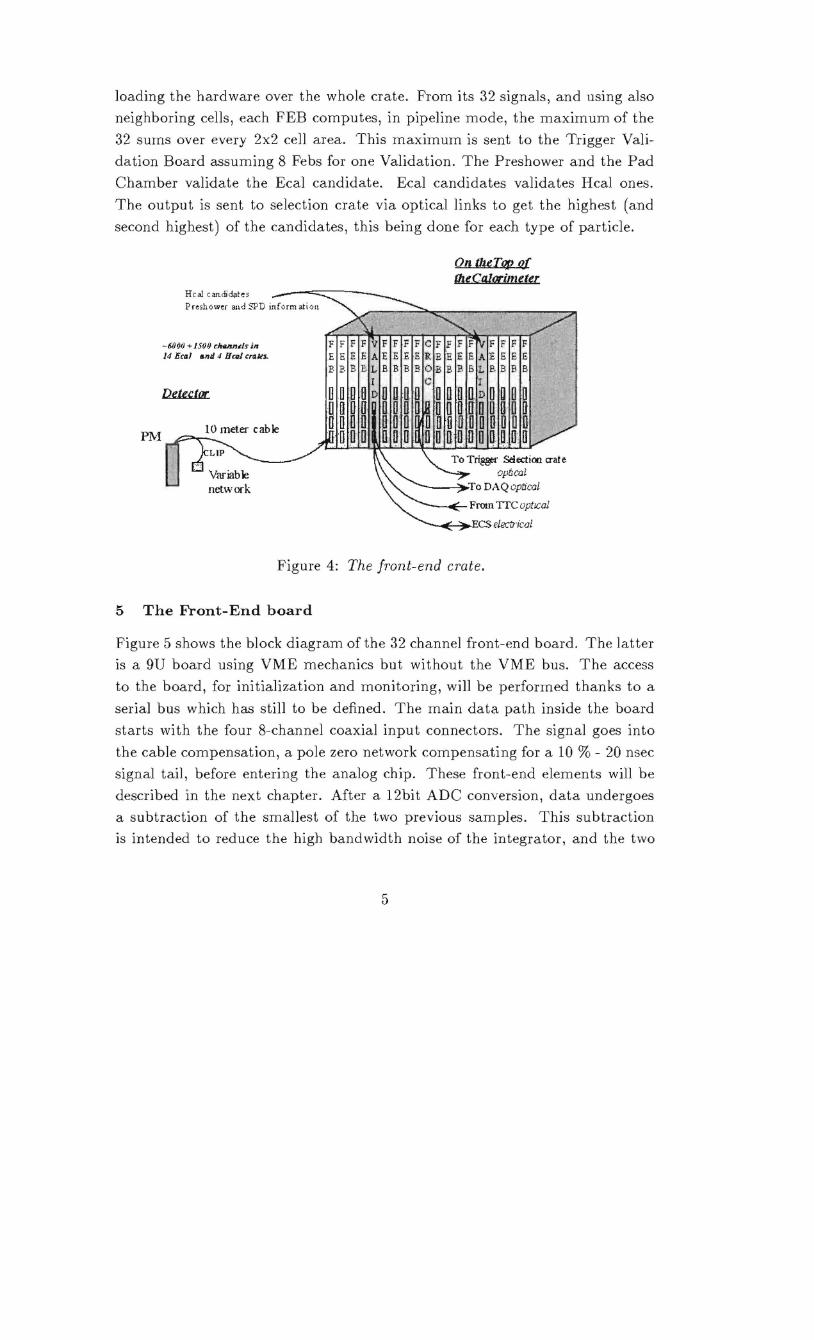
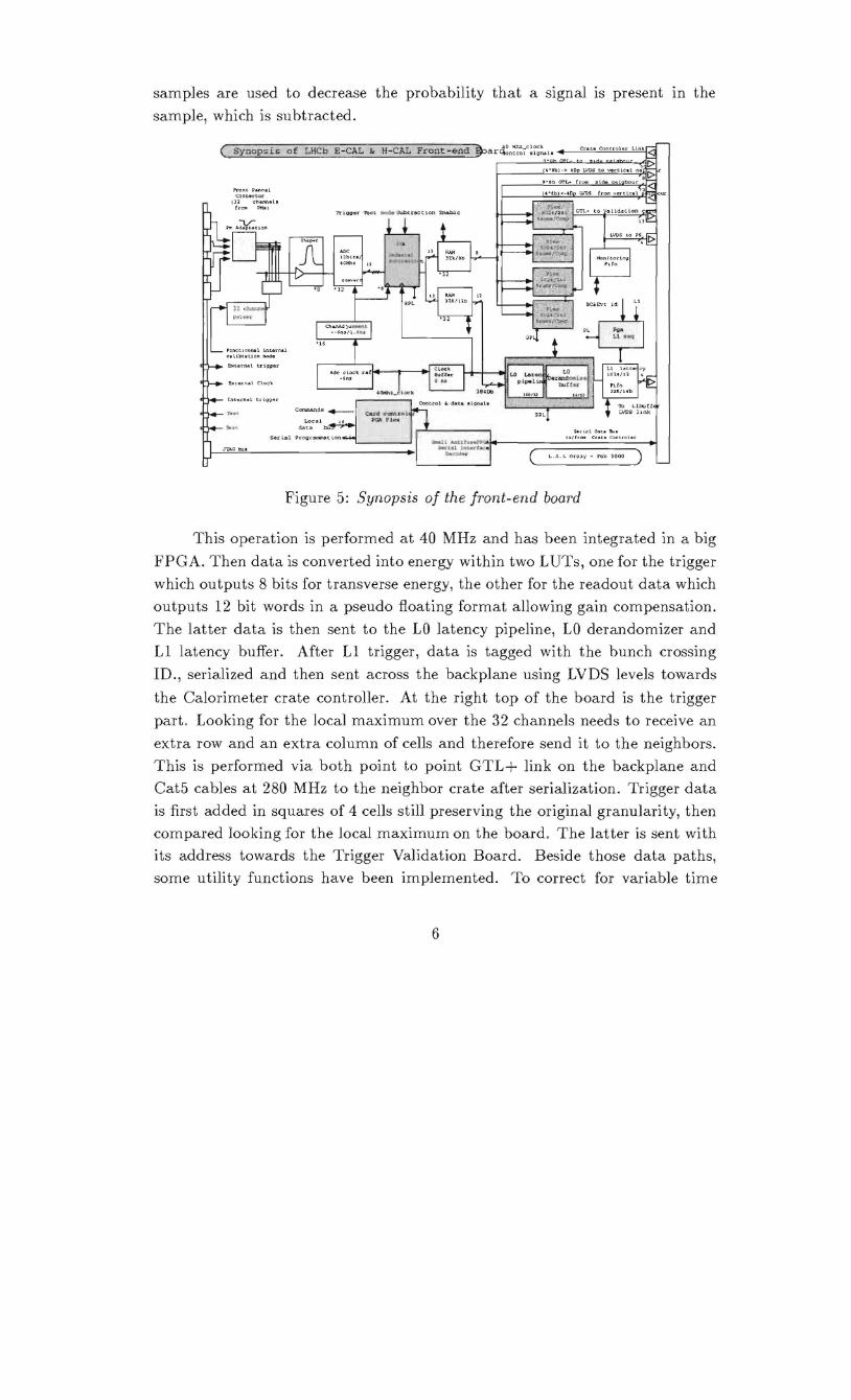
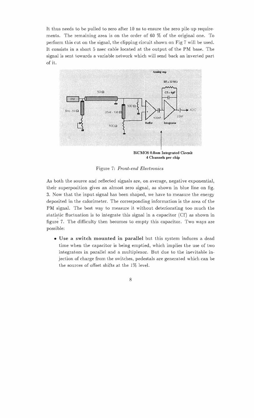
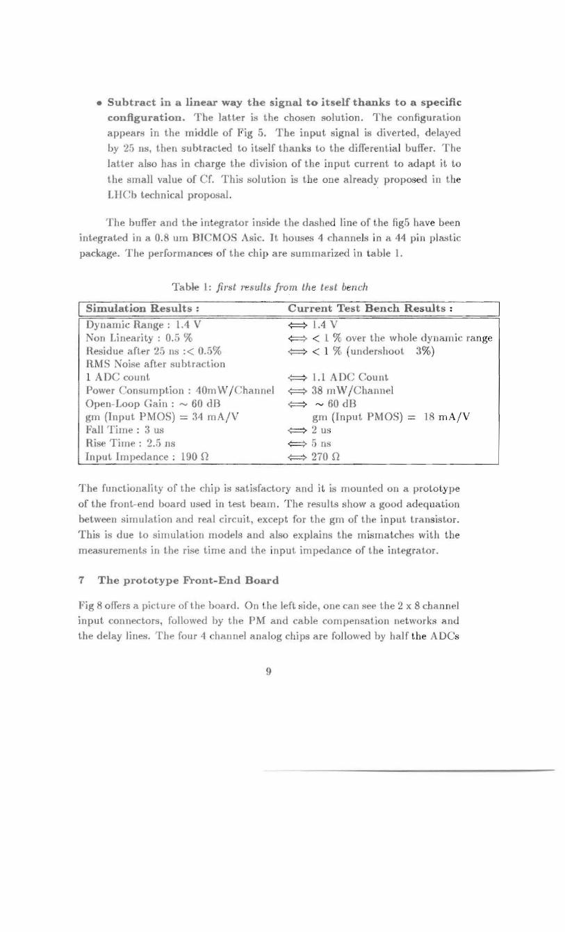
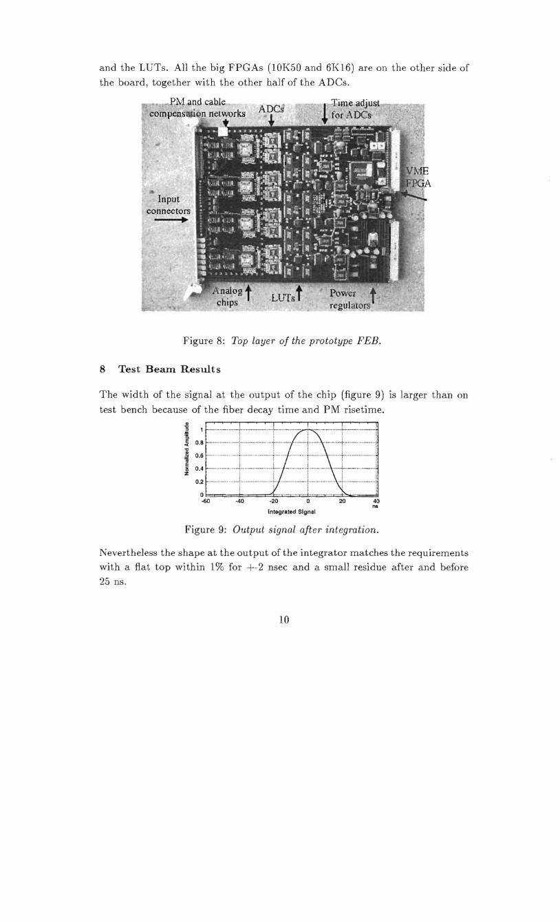
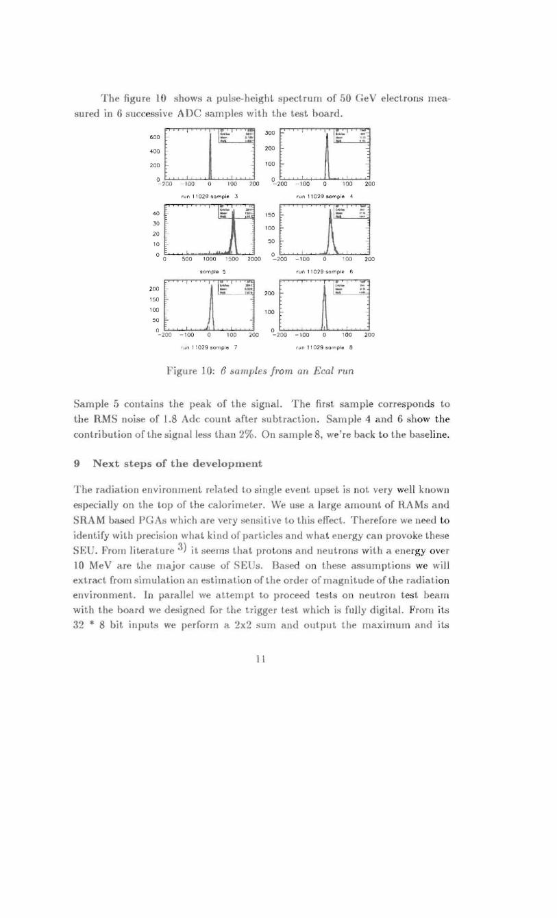