Embed Size (px)
Citation preview
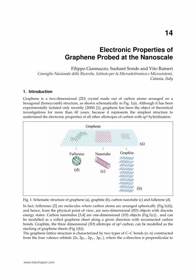
14
Electronic Properties of Graphene Probed at the Nanoscale
Filippo Giannazzo, Sushant Sonde and Vito Raineri Consiglio Nazionale delle Ricerche, Istituto per la Microelettronica e Microsistemi,
Catania, Italy
1. Introduction
Graphene is a two-dimensional (2D) crystal made out of carbon atoms arranged on a hexagonal (honeycomb) structure, as shown schematically in Fig. 1(a). Although it has been experimentally isolated only recently (2004) [1], graphene has been the object of theoretical investigations for more than 60 years, because it represents the simplest structure to understand the electronic properties of all other allotropes of carbon with sp2 hybridisation.
Fig. 1. Schematic structure of graphene (a), graphite (b), carbon nanotube (c) and fullerene (d).
In fact, fullerenes [2] are molecules where carbon atoms are arranged spherically (Fig.1(d)), and hence, from the physical point of view, are zero-dimensional (0D) objects with discrete energy states. Carbon nanotubes [3,4] are one-dimensional (1D) objects (Fig.1(c)) , and can be modelled as a rolled graphene sheet along a given direction with reconnected carbon bonds. Graphite, the three dimensional (3D) allotrope of sp2 carbon, can be modelled as the stacking of graphene sheets (Fig.1(b)). The graphene lattice structure is characterized by two types of C–C bonds (σ, π) constructed from the four valence orbitals (2s, 2px , 2py , 2pz ), where the z-direction is perpendicular to
www.intechopen.com
Physics and Applications of Graphene - Experiments
354
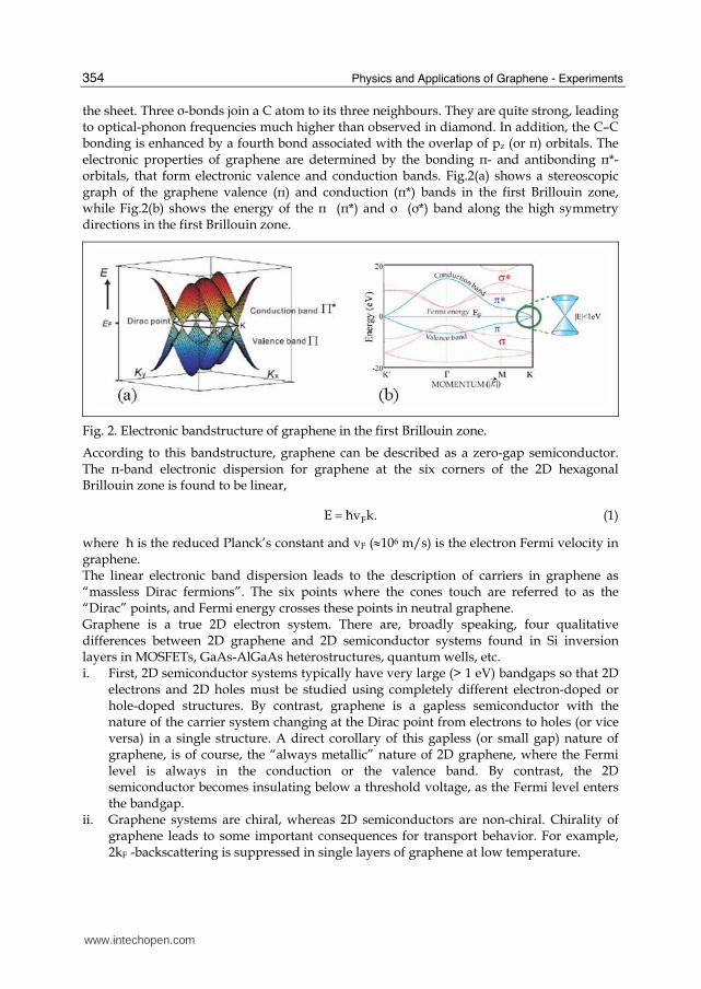
the sheet. Three σ-bonds join a C atom to its three neighbours. They are quite strong, leading to optical-phonon frequencies much higher than observed in diamond. In addition, the C–C bonding is enhanced by a fourth bond associated with the overlap of pz (or π) orbitals. The electronic properties of graphene are determined by the bonding π- and antibonding π*-orbitals, that form electronic valence and conduction bands. Fig.2(a) shows a stereoscopic graph of the graphene valence (π) and conduction (π*) bands in the first Brillouin zone, while Fig.2(b) shows the energy of the π (π*) and σ (σ*) band along the high symmetry directions in the first Brillouin zone.
Fig. 2. Electronic bandstructure of graphene in the first Brillouin zone.
According to this bandstructure, graphene can be described as a zero-gap semiconductor. The π-band electronic dispersion for graphene at the six corners of the 2D hexagonal Brillouin zone is found to be linear,
FE ћv k.= (1)
where ħ is the reduced Planck’s constant and vF (≈106 m/s) is the electron Fermi velocity in graphene. The linear electronic band dispersion leads to the description of carriers in graphene as “massless Dirac fermions”. The six points where the cones touch are referred to as the “Dirac” points, and Fermi energy crosses these points in neutral graphene. Graphene is a true 2D electron system. There are, broadly speaking, four qualitative differences between 2D graphene and 2D semiconductor systems found in Si inversion layers in MOSFETs, GaAs-AlGaAs heterostructures, quantum wells, etc. i. First, 2D semiconductor systems typically have very large (> 1 eV) bandgaps so that 2D
electrons and 2D holes must be studied using completely different electron-doped or hole-doped structures. By contrast, graphene is a gapless semiconductor with the nature of the carrier system changing at the Dirac point from electrons to holes (or vice versa) in a single structure. A direct corollary of this gapless (or small gap) nature of graphene, is of course, the “always metallic” nature of 2D graphene, where the Fermi level is always in the conduction or the valence band. By contrast, the 2D semiconductor becomes insulating below a threshold voltage, as the Fermi level enters the bandgap.
ii. Graphene systems are chiral, whereas 2D semiconductors are non-chiral. Chirality of graphene leads to some important consequences for transport behavior. For example, 2kF -backscattering is suppressed in single layers of graphene at low temperature.
www.intechopen.com
Electronic Properties of Graphene Probed at the Nanoscale
355
iii. Monolayer graphene dispersion is linear, whereas 2D semiconductors have quadratic energy dispersion. This leads to substantial quantitative differences in the transport properties of the two systems.
iv. Finally, the carrier confinement in graphene is ideally 2D, since the graphene layer is precisely one atomic monolayer thick. For 2D semiconductor structures, the quantum dynamics is two dimensional by virtue of confinement induced by an external electric field, and as such, 2D semiconductors are quasi-2D systems, and always have an average width or thickness <t> (≈ 5 nm to 50 nm) in the third direction with <t>≤ ┣F, where ┣F is the 2D Fermi wavelength (or equivalently the carrier de Broglie wavelength). The condition <t> < ┣F defines a 2D electron system. In particular, for
graphene, we have ┣F ≈ (2×10⁷√π/√n) nm, where n is the carrier density in cm−2, and since t ≈ 0.1 nm to 0.2 nm (the monolayer atomic thickness), the condition ┣F>t is always satisfied, even for an unphysically large n=1014 cm−2.
The classic technique to verify the 2D nature of a particular system is to show that the orbital
electronic dynamics is sensitive only to a magnetic field perpendicular to the 2D plane of
confinement. Therefore, the observation of magnetoresistance oscillations (Shubnikov-de
Hass effect) proves the 2D nature. The most definitive evidence for 2D nature, however, is
the observation of the quantum Hall effect, which is a quintessentially 2D phenomenon.
Any system manifesting an unambiguous quantized Hall plateau is 2D in nature, and
therefore the observation of the quantum Hall effect in graphene in 2005 by Novoselov et al.
[5] and Zhang et al. [6] is an absolute evidence of its 2D nature. In fact, the quantum Hall
effect in graphene persists to room temperature [7], indicating that graphene remains a strict
2D electronic material even at room temperature.
1.1 Graphene for electronic applications: opportunities and challenges Graphene has been adopted as a material of choice by researchers involved in many fields.
In particular, simultaneous observation of high mobility, sensitivity to field effect and ease
of contacting made graphene an appealing candidate for field-effect transistor devices. A lot
of progress has been made in that direction. Manufacturability of graphene transistor
operating at 100 GHz has been demonstrated on wafer-scale [8]. Moreover, chemically
stable, robust and foldable graphene sheets possess enough optical transparency to be
considered as transparent conductors in applications as coatings for solar cells, liquid crystal
displays etc. for the replacement for indium tin oxide [9].
However some open issues still remain and are currently the object of intense research
activity.
i. Although the “intrinsic” mobility of graphene has been estimated to be >2×105 cm2V-1s-
1, the mobility values commonly reported in the literature span a wide range, from ~102 to ~104 cm2V-1s-1, depending on the synthesis method used to obtain graphene, on the kind of substrate where it is deposited, etc… It is evident that the intrinsically outstanding transport properties of this material are limited by extrinsic mechanisms. However, there is no consensus about the scattering mechanism that currently limits the mobility in graphene devices;
ii. Due to the zero bandgap of graphene electronic structure, it is not possible to reach high values of the ratio Ion/Ioff between the on state and off state current in graphene field effect devices. To date several strategies have been developed to open a gap in graphene electronic bandstructure. Among them, the following must be cited.
www.intechopen.com

Physics and Applications of Graphene - Experiments
356
a. The inclusion of sp3 hydrocarbon defects in the sp2 lattice [10], b. The distortion of the graphene lattice under uniaxial strain [11D], c. The application of a transversal electric field to a bilayer graphene [12], d. The influence of the SiC substrate on the epitaxial graphene on Si face of hexagonal SiC
has also been shown to induce substantial band gap [13], e. Moreover, a bandgap can also be induced in semimetallic graphene if it is shaped in
nanoribbons by a direct consequence of the lateral confinement of the 2DEG [14]. However, this points to extremely challenging need to perform atomically precise tailoring of graphene over long distances for advanced graphene electronic architectures.
1.3 Need for a nanoscale control of graphene electronic properties As ongoing efforts to incorporate graphene into electronic applications, attempts are already
being made to gain consistent control over electronic properties in graphene down to
nanometer scale so as to explore its possibility as a complementary material to Silicon for
prospective nanoelectronics. Notable amongst these include intentional control of the
density and character of its charge carriers by doping [15], and confining charge carriers to
nanometer constrictions [14]. Typically, most experiments probe the global electrical
response of graphene devices thus yielding properties averaged over the whole device. As a
consequence, local properties and their distributions within the sample are inaccessible with
standard electron transport measurements. In low dimensional electronic systems, like
graphene, the local phenomenona/effects might have much stronger impact than previously
believed. Hence, naturally, developing techniques to analyse and/or control the local effects
in graphene has attracted wide interests. Consequently, such local probing techniques have
helped gain significant insights into various aspects of functioning graphene devices.
Notably, scanning probe microscopy (SPM) based measurements have provided the most
direct probe of local electronic properties. For example, Scanning Photocurrent Microscopy
[16] has been used to probe the ‘electrostatic potential landscape’ of graphene in view of
analyzing the local changes in the electronic structure of the graphene sheets introduced by
their interaction with deposited metal contacts and by local symmetry breaking/ disorder at
the sheet edges. On the other hand Raman microscopy has been used to probe mesoscopic
inhomogeneity in the doping [17], due, possibly, to the presence of charged impurities.
Formation of sub-micron (resolution limited) electron and hole charge puddles near Dirac
point in graphene, has been demonstrated by Martin et. al. [18] using Scanning Single
Electron Transistor microscopy where they gauged the intrinsic size of the puddles to be ~30
nm. Atomic Force Microscope based scanning microscopy techniques have also been
significantly used to get better insights in graphene electronic properties. For example, high-
resolution scanning tunneling microscopy (STM) [19D] experiments have directly imaged
charge puddles of ~10 nm in size and suggested they originate from individual charged
impurities underneath graphene.
In the wake of such proven local inhomogeneity in electrical properties of graphene the work presented in this chapter focuses on local evaluation of transport properties in substrate-supported graphene by the use of scanning probe microscopy based methods with nanometer scale lateral resolution. In particular Section 2 deals with the most common graphene synthesis methods and, in particular, on those used in this study, i.e. mechanical exfoliation of HOPG and epitaxial
www.intechopen.com

Electronic Properties of Graphene Probed at the Nanoscale
357
growth by thermal treatments on hexagonal SiC. The characterization methods used for the identification and morphological and structural analyses of the produced graphene layers are also illustrated Section 3 is focused on the evaluation of the local transport properties, electron mean free path and mobility, in graphene on insulating and semiconducting substrates. In particular the role of the interaction of 2DEG in graphene with the substrate (in particular, the role of dielectric environment) is discussed.
2. Graphene synthesis methods Graphene has been adopted as a material of interest quite widely. This had led to many
motivations for material synthesis. To date, the synthetic techniques fall into two categories.
In the first approach the weak bonding between the graphene layers in HOPG is exploited
and single or few layers of graphene are separated from the parent crystal either by
mechanical [1] or chemical exfoliation [20]. Mechanical separation, the technique used to
obtain and study graphene in the laboratory for the first time [1], is a simple, inexpensive
method, yielding graphene flakes of very high crystalline quality. However, the yield of
graphene production is extremely low and the flakes have small dimension (from 1 μm to
100 μm lateral size), so that this approach lacks the scalability required by mass device
production. Exfoliation of graphene in solution from HOPG by chemical methods allows to
improve the yield, but the size of the flakes remains too small and the crystalline quality is
worse than in mechanically exfoliated graphene.
The second approach is based on the epitaxial growth of graphene on substrates. In
particular, graphene has been obtained by chemical vapour deposition on catalytic metal
films (Ni, Cu,..) from hydrocarbon precursors [21,22], or by controlled thermal
decomposition of SiC [23]. This second approach has the potential of producing large-area
lithography-compatible films and is rapidly advancing at the moment. The crystalline
quality of epitaxial graphene is typically lower than in mechanically exfoliated graphene
flakes, but it could be improved by improving the growth methods. In the case of graphene
grown on metal substrates, the grown film needs to be transferred to an insulating substrate,
to be useful in electronic applications. On the contrary, epitaxial graphene obtained by
thermal treatments of SiC grows directly on a semiconducting or semiinsulating substrate,
and is expecially suitable for electronic applications.
In the present study, the used graphene samples were obtained by mechanical exfoliation of HOPG and by epitaxial growth on hexagonal SiC substrate. The sample preparation and graphene identification for the two methods are discussed in the following.
2.1 Mechanical exfoliation of HOPG Mechanical exfoliation, developed by Novoselov and Geim [1], involves a topdown
approach to get graphene from highly oriented pyrolitic graphite (HOPG). Using a common
adhesive tape a thin graphite layer is peeled off from HOPG. With an inter-layer van der
Waals interaction energy of about 2 eV/nm2, the force required to exfoliate graphite is
extremely weak, about 300 nN/┤m2. After repeated thinning the flakes are transferred by
gently pressing the tape onto suitable substrate. We used extensive characterization by
Optical contrast microscopy imaging (OM), TappingMode AFM (t-AFM), and microRaman
(┤R) spectroscopy to analyze/identify manolayer flakes.
www.intechopen.com

Physics and Applications of Graphene - Experiments
358
Fig. 3. Optical microscopy image (a), micro-Raman spectra (b) and atomic force microscopy (c) image of few layers of graphene obtained by mechanical exfoliation of HOPG (Data from Ref. [24].)
In Fig. 3(a), an OM image of a FLG sample is reported [24]. The variable contrast in the
image is indicative of a variable number of layers in the different regions of the sample. In
particular, a lower contrast is associated to thinner layers. After an appropriate calibration,
optical contrast variations can be used for a quantitative determination of the number of
layers. In Fig.3(b), ┤R spectra measured on some selected positions indicated by the red,
green and blue dots in the OM of Fig. 3(a) are shown. As a reference, the spectrum obtained
from HOPG is also reported. Raman spectroscopy is a very powerful method for the
characterization of HOPG and FLG. In particular, it allows an unambiguous distinction
between single layer, bilayer and multilayers in the case of graphene obtained by exfoliation
of HOPG [25]. This is possible through a comparison of the relative intensity of the
characteristics G peak (appearing at ~1580 cm-1) and 2D peak (appearing at ~2680 cm-1) and
from the symmetry of the 2D peak in the Raman spectra. As it is evident from Fig.3(b), the
spectrum measured in the flake region with the lowest optical contrast (position indicated
by a red point in Fig.3(a)), exhibits a symmetric 2D peak with very high intensity compared
with the G peak. These characteristic spectroscopic features have been associated uniquely
to a graphene single layer. As it is evident, the relative intensity of the two peaks is very
different in the case of a graphene bilayer, for which the 2D peak is not symmetric. For a
number of layers larger than three the Raman spectrum becomes qualitatively similar to that
of HOPG.
In Fig.4(a), an AFM morphological image on the same sample region as in Fig.3(a) is
reported. In order to obtain quantitative information on the number of graphene layers from
these morphological image, a height profile along the dashed line indicated in Fig.4(a) is
reported in Fig.4(b). The zero height value is represented by the SiO2 surface level. Hence,
from the profile in Fig.4b it is possible to deduce the height associated to the single layer,
bilayer and trilayer of graphene previously identified by Raman spectroscopy.
Interestingly, the measured height of a single layer with respect to the SiO2 is ~0.7 nm, while the relative heights of the second layer with respect to the first one and that of the third layer with respect to the second are both ~0.35 nm. The latter thickness value is very close to the interlayer spacing between graphene planes within HOPG. Hence, it seems that the measured step-height for a single layer of graphene is affected by an “offset”. This means that, in order to use AFM to determine the number of graphene layer in a sheet, it is
www.intechopen.com

Electronic Properties of Graphene Probed at the Nanoscale
359
(c)(c)
Fig. 4. AFM morphological image of a FLG (a) and height profile along the indicated dashed
line (b). Average height h as a function of the estimated number of layers n (c). The data
have been fitted with the linear relation, h=tgr×n+t0, with the interlayer spacing tgr and the
offset t0 fitting parameters. The best fit with the experimental data obtained for the values of
tgr=0.36±0.01 nm and t0=0.28±0.06 nm (Data from Ref. [24]).
necessary to have an accurate estimate of this value. To do this, the step height with respect
to SiO2 was measured on a large number of flakes with variable number of layers, and with
a “staircase” structure similar to that illustrated in Fig.4(b). For each flake, the single layer
region was unambiguously determined by ┤R measurements. The number of layers for
thicker regions could be obtained by counting the number of subsequent steps with ~0.35
nm height. In Fig.4c, the average height h is reported as a function of the estimated number
of layers n. These data have been fitted with the linear relation, h=tgr×n+t0, where the
interlayer spacing tgr and the offset t0 are the fitting parameters. The best fit with the
experimental data has been obtained for the values of tgr=0.36±0.01 nm and t0=0.28±0.06 nm.
Based on such calibration curve (measured height versus number of layers), it is possible to
determine in an accurate and straightforward way the number of layers in a multilayer
sheet deposited on thermal SiO2 by an AFM analysis. However, this calibration procedure
has to be repeated if the substrate material is changed, since the offset t0 depends on the
specific substrate.
Quantitative information on number of graphene layers deposited on a substrate can also be
obtained from optical images, if an accurate analysis of the contrast is carried out. The
optical contrast C can be quantitatively defined as,
sub gr subC (R R ) /R= − (2)
where Rgr is the reflected light intensity by FLG and Rsub the reflected intensity by the
substrate[26]. Typically a SiO2/Si substrate with 100 or 300 nm thick SiO2 is chosen, since for
these thicknesses optical contrast is maximized for light wavelengths in the visible range
(400-700 nm), due to a constructive interference effect.
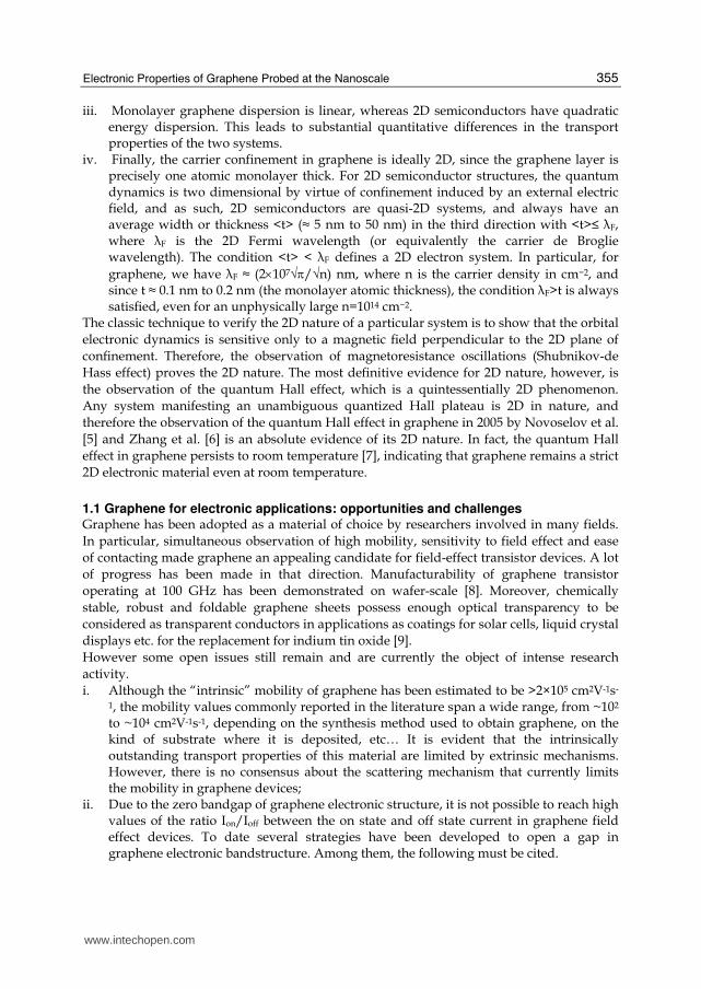
Fig. 5(a) and (b) illustrate the procedure to extract the optical contrast from an OM on a
single layer of graphene flake deposited on 100 nm thick SiO2 and illuminated with light of
600 nm wavelength [24]. Based on this procedure, the optical contrast can be determined for
flakes of different thickness. The number of layers in the flakes can be independently
determined by AFM according to the calibration curve in Fig.4 (c). In Fig.5(c), the symbols
represent the contrast as a function of the flake thickness (and the number of graphene
www.intechopen.com
Physics and Applications of Graphene - Experiments
360
(a)(b)
(c)
(a)(b)
(a)(b)
(c)(c)
Fig. 5. Optical image of a SLG (a), reflected intensity profile along the dashed line (b) and optical contrast versus the number of graphene layers for two different incident light wavelengths (c) (Data from Ref. [24]).
layers) for samples deposited on 300 nm SiO2 and illuminated with light of 400 nm (black
triangles) and 600 nm (red squares) wavelengths. The lines represent the calculated contrast
as a function of the number of layers. The reflected light intensities Rsub and Rgr are
calculated using the Fresnel equations. The literature values of the complex refraction index
of Si and SiO2 as a function of the wavelength were used.
For graphene, the real and imaginary part of the refraction index ngr were calculated starting
from its noticeable absorption properties in the wavelength range of visible light. In fact,
recently, it has been shown that a single layer of graphene absorbs a fixed percentage (πα=
2.3%, where α is the fine structure constant) of the intensity of incident visible light [27].
Moreover, for few layers of graphene, the absorbance increases linearly with the number of
layers. Based on these properties, refraction index values of graphene for the two considered
wavelengths were calculated to be:
(400 ) 2.57 0.81= −grn nm i (3.a)
(600 ) 2.53 1.21= −grn nm i (3.b)
2.2 Epitaxial growth of graphene of SiC Graphene growth during annealing of SiC relies on the interplay of two different
mechanisms: (i) the preferential Si sublimation from SiC surface, which leaves an excess of C
atoms in the near surface region, and (ii) the diffusion of these C atoms on the SiC surface
www.intechopen.com
Electronic Properties of Graphene Probed at the Nanoscale
361
and their reorganization in the two dimensional graphene lattice structure. Both
mechanisms depend in a complex way both on the annealing conditions (temperature Tgr,
ramp rate, pressure in the chamber) and on the initial surface conditions of SiC wafers, e.g.
the termination (Si or C –face), the miscut angle, the defectivity. It has been shown that the
rate of Si evaporation can be strongly reduced by performing the annealing in inert gas
ambient at atmospheric pressure instead than in vacuum [28]. This results in the possibility
to raise the growth temperature, from typical values of Tgr∼1300°C in vacuum to Tgr>1600°C
at atmospheric pressure [29]. This has, in turns, beneficial effects on the crystalline quality of
the EG layers, since at higher temperature a higher diffusivity of the C atoms on the surface
is achieved. It has been also observed that graphene growth starts from the kinks of terraces
on the SiC surface or from defects (e.g. pits or threading dislocations) [30]. This means that,
for fixed annealing conditions, a higher growth rate is expected on vicinal, i.e. off-axis, SiC
surfaces than on on-axis ones, since the spacing between terraces kinks is reduced. Most of
the studies on EG growth reported in the literature were carried out on on-axis hexagonal
SiC substrates.
200nm
Hei
gh
t (n
m)
2.0
0.0
(a)
200nm
Hei
gh
t (n
m)
2.0
0.0200nm
Hei
gh
t (n
m)
2.0
0.0200nm
Hei
gh
t (n
m)
2.0
0.0
(a)
0.0 0.2 0.4 0.6 0.8 1.0
0.0
0.5
1.0
1.5
2.0 30 nm
Heig
ht
(nm
)
L (μm)
(b)
0.0 0.2 0.4 0.6 0.8 1.0
0.0
0.5
1.0
1.5
2.0 30 nm
Heig
ht
(nm
)
L (μm)0.0 0.2 0.4 0.6 0.8 1.0
0.0
0.5
1.0
1.5
2.0 30 nm
Heig
ht
(nm
)
L (μm)
(b)
200nm
Hei
gh
t (n
m)
2.0
0.0
(a)
200nm
Hei
gh
t (n
m)
2.0
0.0200nm
Hei
gh
t (n
m)
2.0
0.0200nm
Hei
gh
t (n
m)
2.0
0.0
(a)
0.0 0.2 0.4 0.6 0.8 1.0
0.0
0.5
1.0
1.5
2.0 30 nm
Heig
ht
(nm
)
L (μm)
(b)
0.0 0.2 0.4 0.6 0.8 1.0
0.0
0.5
1.0
1.5
2.0 30 nm
Heig
ht
(nm
)
L (μm)0.0 0.2 0.4 0.6 0.8 1.0
0.0
0.5
1.0
1.5
2.0 30 nm
Heig
ht
(nm
)
L (μm)
(b)
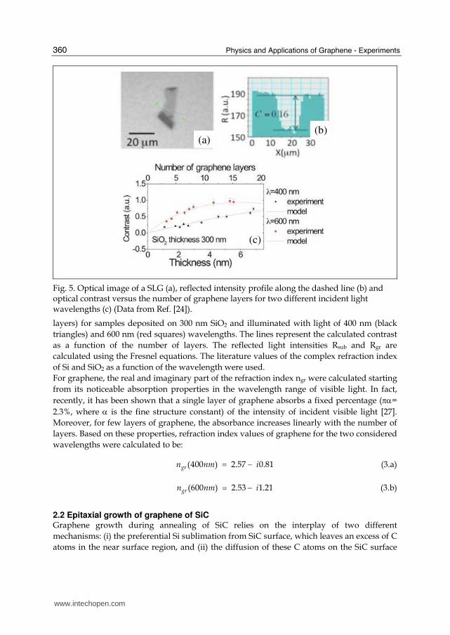
Fig. 6. AFM morphological image of a virgin 4H-SiC (0001), 8° off-axis surface (a) and
linescan (b), showing the parallel terraces with a mean width of ∼30 nm (Data from Ref. [31]).
The results here reported concern EG grown on the Si face of 8° off-axis 4H-SiC by
annealing in inert gas (Ar) ambient in a wide range of temperatures (Tgr from 1600°C to
2000°C) [31]. A morphological AFM image of the virgin 4H-SiC (0001) surface is reported
in Fig.6, showing the parallel terraces oriented in the <00-10> direction and with a mean
width of ∼30 nm. AFM images of the surface morphology for the samples annealed at
1600, 1700 and 2000 °C are reported in Fig.7(a), (b) and (c), whereas the corresponding
phase maps on the same samples are reported in Fig.7(d), (e) and (f). Annealed samples
show wide terraces (average width of ~150-200 nm) running parallel to the original steps
in the virgin sample.
Such large terraces are the result of the step-bunching commonly observed on off-axis SiC
substrates after thermal treatments at temperatures >1400°C. Interestingly, a network of
nanometer wide linear features is superimposed to these large terraces. These features are
particularly evident in the phase images of the surfaces.
www.intechopen.com

Physics and Applications of Graphene - Experiments
362
Phas
e
0
20°
Hei
ght
(nm
)
0
30
200 nm
(a) (b) (c)
(d) (e) (f)
Phas
e
0
20°
Phas
e
0
20°
Hei
ght
(nm
)
0
30
Hei
ght
(nm
)
0
30
200 nm200 nm
(a) (b) (c)
(d) (e) (f)
Fig. 7. AFM images of the surface morphology for the samples annealed at 1600 (a), 1700 (b) and 2000 °C (c). The corresponding phase maps on the same samples are reported in (d), (e) and (f). (Data from Ref. [31]).
Fig.8 shows two representative linescans taken in the direction orthogonal (b) and parallel (c) to the terraces length obtained from the morphology map of the sample annealed at 1700°C. In the orthogonal direction, it is worth noting very small steps with nm or sub-nm height, which are overlapped to the large terraces of the SiC substrate. The height of these steps is always a multiple of 0.35 nm, the height value corresponds the interlayer spacing
between two stacked graphene planes in HOPG. As an example a ∼0.35 nm and a ∼1.1 high step are indicated in Fig.8(b), associated, respectively, to one and three graphene layers over the substrate or stacked over other graphene layers. From the linescan in the direction parallel to the terraces length (c), peculiar corrugations
with ∼2 nm typical height can be observed.
30
0
Hei
gh
t (n
m)
200 nm
(a)
200 300 400 500 6000
5
10
15
20
25
~1.1~0.35
Heig
ht
(nm
)
X (nm)
(c)
0 100 200 300
4
5
6
7
~2 nm
Y (nm)
(d)
30
0
Hei
gh
t (n
m)
200 nm
(a)30
0
Hei
gh
t (n
m)
200 nm
30
0
Hei
gh
t (n
m)
200 nm200 nm
(a)
200 300 400 500 6000
5
10
15
20
25
~1.1~0.35
Heig
ht
(nm
)
X (nm)
(c)
200 300 400 500 6000
5
10
15
20
25
~1.1~0.35
Heig
ht
(nm
)
X (nm)
(c)
0 100 200 300
4
5
6
7
~2 nm
Y (nm)
(d)
0 100 200 300
4
5
6
7
~2 nm
Y (nm)
(d)(b) (c)
30
0
Hei
gh
t (n
m)
200 nm
(a)
200 300 400 500 6000
5
10
15
20
25
~1.1~0.35
Heig
ht
(nm
)
X (nm)
(c)
0 100 200 300
4
5
6
7
~2 nm
Y (nm)
(d)
30
0
Hei
gh
t (n
m)
200 nm
(a)30
0
Hei
gh
t (n
m)
200 nm
30
0
Hei
gh
t (n
m)
200 nm200 nm
(a)
200 300 400 500 6000
5
10
15
20
25
~1.1~0.35
Heig
ht
(nm
)
X (nm)
(c)
200 300 400 500 6000
5
10
15
20
25
~1.1~0.35
Heig
ht
(nm
)
X (nm)
(c)
0 100 200 300
4
5
6
7
~2 nm
Y (nm)
(d)
0 100 200 300
4
5
6
7
~2 nm
Y (nm)
(d)(b) (c)
Fig. 8. Two representative linescans from the morphology map (a) of a sample annealed at 1700°C taken in the direction orthogonal (b) and parallel (c) to the steps. (Data from Ref. [31]).
www.intechopen.com

Electronic Properties of Graphene Probed at the Nanoscale
363
5 nm5 nm
(a)
10 nm
(b)
10 nm 10 nm5 nm5 nm
(a)
10 nm10 nm
(b)
10 nm10 nm 10 nm10 nm
Fig. 9. Two representative HRXTEM images for 8° off-axis 4H-SiC (0001) annealed at 2000 °C. (Data from Ref. [31]).
HRXTEM analyses allowed to get further insight on the structural properties of the graphene films grown at the different temperatures and to clarify the nature of these peculiar corrugations. In Fig.9(a) and (b) two representative HRXTEM images for a sample annealed at 2000 °C are reported. From Fig.9(a), it is evident that a graphene multilayer uniformly covers the SiC surface also on the terrace step edges. From Fig.9(b), the structure of one of the peculiar corrugations running orthogonal to the steps is reported. This cross sectional image unambiguously demonstrate that those features are wrinkles in the multilayer graphene film. These peculiar defects have been observed also by other authors in the case of few layers of graphene grown on the C face [32] or on the Si face [33] of hexagonal SiC, on-axis. However, in that case wrinkles do not exhibit any preferential orientation with respect to the steps, but form an isotropic mesh-like network on the surface, where wrinkles are interconnected into nodes (typically three wrinkles merge on a node and the angles subtended by the wrinkles are ~60° or 120 °C [32]). The formation of that mesh-like network of wrinkles was attributed to the release of the compressive strain which builds up in FLG during the sample cooling due to mismatch between the thermal expansion coefficients of graphene and the SiC substrate [32]. Comparing the morphology and phase images in Fig.7 for the samples annealed at the different temperatures, it is easy to observe that the density of wrinkles increases with temperature.
2 nm2 nm
1700 °C
2 nm2 nm SiC
Glue
1600 °C
2 nm2 nm
2000 °C
(a) (b)(c)
2 nm2 nm
1700 °C
2 nm2 nm
1700 °C
2 nm2 nm SiC
Glue
1600 °C
2 nm2 nm SiC
Glue
1600 °C
2 nm2 nm
2000 °C
(a) (b)(c)
Fig. 10. HRXTEM images on the samples annealed at 1600 (a), 1700 (b) and 2000°C (c) are reported, showing 3, 8 and 18 layers on the surface of 4H-SiC. (Data from Ref. [31]).
www.intechopen.com
Physics and Applications of Graphene - Experiments
364
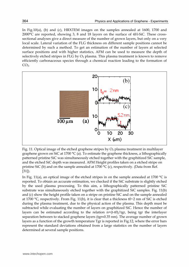
In Fig.10(a), (b) and (c), HRXTEM images on the samples annealed at 1600, 1700 and 2000°C are reported, showing 3, 8 and 18 layers on the surface of 4H-SiC. These cross-sectional analyses give a direct measure of the number of grown layers, but only on a very local scale. Lateral variation of the FLG thickness on different sample positions cannot be determined by such a method. To get an estimation of the number of layers at selected surface positions and with higher statistics, AFM can be used to measure the depth of selectively etched stripes in FLG by O2 plasma. This plasma treatment is known to remove efficiently carbonaceous species through a chemical reaction leading to the formation of CO2.
0
t0=
t
(b)
(c)
(a)100 μm
0
t0=
t
(b)
(c)
(a)100 μm (a)100 μm100 μm
Fig. 11. Optical image of the etched graphene stripes by O2 plasma treatment in multilayer graphene grown on SiC at 1700 °C (a). To estimate the graphene thickness, a lithographically patterned pristine SiC was simultaneously etched together with the graphitized SiC sample, and the etched SiC depth was measured. AFM Height profiles taken on a etched stripe on pristine SiC (b) and on the sample annealed at 1700 °C (c), respectively. (Data from Ref. [31]).
In Fig. 11(a), an optical image of the etched stripes in on the sample annealed at 1700 °C is reported. To obtain an accurate estimation, we checked if the SiC substrate is slightly etched by the used plasma processing. To this aim, a lithographically patterned pristine SiC substrate was simultaneously etched together with the graphitized SiC samples. Fig. 11(b) and (c) show the height profile taken on a stripe on pristine SiC and on the sample annealed at 1700 °C, respectively. From Fig. 11(b), it is clear that a thickness t0~2 nm of SiC is etched during the plasma treatment, due to the physical action of the plasma. This depth must be subtracted while evaluating the number of layers on graphitized SiC. Hence the number of layers can be estimated according to the relation n=(t-t0)/tgr, being tgr the interlayer
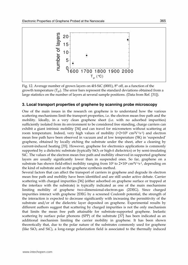
separation between to stacked graphene layers (tgr≈0.35 nm). The average number of grown layers as a function of the growth temperature Tgr is reported in Fig.12, where the error bars represent the standard deviations obtained from a large statistics on the number of layers determined at several sample positions.
www.intechopen.com
Electronic Properties of Graphene Probed at the Nanoscale
365
1600 1700 1800 1900 20000
5
10
15
20
nu
mb
er
of
laye
rs
Tgr
(°C)
Fig. 12. Average number of grown layers on 4H-SiC (0001), 8° off, as a function of the growth temperature (Tgr). The error bars represent the standard deviations obtained from a large statistics on the number of layers at several sample positions. (Data from Ref. [31]).
3. Local transport properties of graphene by scanning probe microscopy
One of the main issues in the research on graphene is to understand how the various scattering mechanisms limit the transport properties, i.e. the electron mean free path and the mobility. Ideally, in a very clean graphene sheet (i.e. with no adsorbed impurities) sufficiently isolated from its environment to be considered free standing, charge carriers can exhibit a giant intrinsic mobility [34] and can travel for micrometers without scattering at room temperature. Indeed, very high values of mobility (>2×105 cm2V-1s-1) and electron mean free path have been observed in vacuum and at low temperature (5K) in ‘suspended’ graphene, obtained by locally etching the substrate under the sheet, after a cleaning by current-induced heating [35]. However, graphene for electronics applications is commonly supported by a dielectric substrate (typically SiO2 or high-k dielectrics) or by semi-insulating SiC. The values of the electron mean free path and mobility observed in supported graphene layers are usually significantly lower than in suspended ones. So far, graphene on a substrate has shown field-effect mobility ranging from 102 to 2×104 cm2V-1s-1, depending on the kind of substrate and on the graphene synthesis method. Several factors that can affect the transport of carriers in graphene and degrade its electron mean free path and mobility have been identified and are still under active debate. Carrier scattering with charged impurities [36] (either adsorbed on graphene surface or trapped at the interface with the substrate) is typically indicated as one of the main mechanisms limiting mobility of graphene two-dimensional-electron-gas (2DEG). Since charged impurities interact with graphene 2DEG by a screened Coulomb potential, the strength of the interaction is expected to decrease significantly with increasing the permittivity of the substrate and/or of the dielectric layer deposited on graphene. Experimental results by different authors suggest that scattering by charged impurities is not the only mechanism that limits the mean free path attainable for substrate-supported graphene. Inelastic scattering by surface polar phonons (SPP) of the substrate [37]D has been indicated as an additional mechanism limiting the carrier mobility in graphene. It has been shown theoretically that, due to the polar nature of the substrates commonly used for graphene (like SiO2 and SiC), a long-range polarization field is associated to the thermally induced
www.intechopen.com
Physics and Applications of Graphene - Experiments
366
lattice vibrations at the surface of the substrate (i.e. the SPP). This field electrostatically couples with the 2DEG, resulting in a sizeable degradation of mobility at room temperature. Recently, the experimental evidence of such SPP scattering at room temperature has been reported, based on temperature dependent transport measurements performed on devices in graphene deposited on SiO2 substrate [34]. It has also been predicted that for graphene on SiC, the SPP scattering has a weaker effect on the electron mobility than for graphene on SiO2, due to weaker polarizability of SiC and relatively high phonon frequencies associated with the hard Si-C bonds [37]. As a matter of fact, charged impurities are randomly distributed on the graphene surface. The random distribution of these scattering sources causes local inhomogeneities in the transport properties, which adversely influence the reproducible operation of graphene nanodevices. Under this point of view, nanoscale resolution methods are required to probe the lateral homogeneity of the transport properties in graphene sheets.
3.1 Local electron mean free path Recently, scanning capacitance spectroscopy (SCS) on graphene was applied to determine the "local" electron mean free path l (defined as the average of the distances traveled by electrons
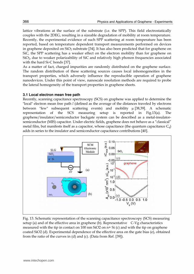
between "few" subsequent scattering events) and mobility μ [38,39]D38. A schematic representation of the SCS measuring setup is reported in Fig.13(a). The graphene/insulator/semiconductor backgate system can be described as a metal-insulator-semiconductor (MIS) capacitor. Under electric fields, graphene does not behave as a “classical” metal film, but manifests itself as a capacitor, whose capacitance (the quantum capacitance Cq) adds in series to the insulator and semiconductor capacitance contributions [40D].
Fig. 13. Schematic representation of the scanning capacitance spectroscopy (SCS) measuring setup (a) and of the effective area in graphene (b). Representative �C-Vg characteristics measured with the tip in contact on 100 nm SiO2 on n+ Si (c) and with the tip on graphene coated SiO2 (d). Experimental dependence of the effective area on the gate bias (e), obtained from the ratio of the curves in (d) and (c). (Data from Ref. [39]).
www.intechopen.com

Electronic Properties of Graphene Probed at the Nanoscale
367
Local measurements were carried out by an AFM, using Pt coated n+-Si tips as probes. A
modulating bias )sin(22
tVV
Vgg ω+=Δ with amplitude Vg and frequency ω=100 kHz was
applied between the Si n+ backgate and the probe. An ultra-high-sensitive (10-21 F/Hz1/2) capacitance sensor connected to the conductive AFM tip allowed to measure, through a lock-in system, the capacitance variation ΔC(Vg) induced by the modulating bias. The AFM tip in contact with bare SiO2 forms a MOS capacitor with capacitance Atip×C’MOS,
where C’MOS is the per unit area capacitance of the MOS system and 2
tiptip rA π= is the tip
contact area with tip radius rtip. When the tip is in contact with graphene, a positive gate bias causes the accumulation of electrons in graphene to screen the positively charged uncompensated ions in the depletion layer at the SiO2/Si interface. On the contrary, a negative gate bias induces the accumulation of holes in graphene to screen the electrons at the SiO2/Si interface. In both cases, the induced carriers in graphene are distributed over an effective area Aeff [40,41] This is schematically illustrated in Fig. 13(b). The total capacitance, when the tip is on graphene, is Ctot=Aeff×C’tot, where C’tot is the series combination of C’MOS and C’q, the per unit area quantum capacitance of graphene. Since C’q>>C’MOS for the typical thicknesses (~100 or ~300 nm) of the adopted SiO2 layers, Ctot can be expressed as Ctot=Aeff×C’MOS. Hence, Ctot/CMOS =Aeff/Atip.
Fig.13(c) and 13(d) show two representative ΔC-Vg characteristics measured with the tip in contact on two distinct positions on a sample with graphene deposited on 100 nm SiO2. The curve in Fig.13(c) was measured with the tip on bare SiO2 and exhibits the typical behavior observed for a MIS capacitor on a n-type semiconductor. The curve in Fig.13(d), measured with the tip on graphene, has a minimum value close to Vg=0 and increases both for negative and positive Vg values. The experimental dependence of the effective area on the gate bias can be obtained from the ratio of the curves in Fig.13(d) and (c), i.e.
MOS
tot
tipeffC
CAA Δ
Δ= (4)
As shown in Fig.13 (e), Aeff exhibits a minimum at Vg~0 and increases linearly with Vg in a symmetric way for both bias polarities. Aeff=πLeff2 represents the effective area of the graphene capacitor responding to the AC bias, i.e. Leff is the distance from the tip contact where the induced screening charges (electrons/holes) spread in graphene. Aeff is much smaller than the area of the entire graphene sheet (~100 μm2 in this specific case). In the following, it is shown that Leff corresponds to the local electron mean free path in the probed graphene region. The induced charge carriers diffuse over a length Leff from the tip contact, traveling at velocity vF. Their diffusivity in graphene can be expressed as D=vFLeff/2. On the other hand, the diffusivity D can be related to electron mobility μ by the generalized Einstein relation D/μ=n/(q∂n/∂EF), being q the electron charge, n the electron density and EF the Fermi energy in graphene. The concepts of mobility and carrier density in graphene are meaningful when the Fermi level is far from the Dirac point but is still in the linear region of the dispersion relation. In these conditions, the density of states is linearly dependent on EF. As a consequence, the carrier density can be expressed as n=EF2/(πħ2vF2), and D/μ=EF/2q. Furthermore, far from the Dirac point, Boltzmann transport theory can be used to describe the electronic transport in graphene and μ can be expressed in terms of l as μ=qvFl/EF. As a consequence, Leff measured by SCS correponds to l. This continuum treatment, using the concepts of diffusivity and mobility and the Einstein relation, is
www.intechopen.com

Physics and Applications of Graphene - Experiments
368
justified on the “mesoscopic” length scale investigated by SCS (from 10 to 100 nm). A quantum mechanical treatment of electron scattering phenomena, based on the interference of incident and reflected electron wavefunctions by a single scattering center, is required on a length scale of ∼1 nm, as recently demonstrated in some investigations by scanning tunneling microscopy [42].
3.2 Role of graphene/substrate interface on the 2DEG transport properties In this section, ‘local’ measurements of the electron mean free path are reported in graphene on most relevant substrates for electronic applications: (i) graphene exfoliated and deposited on 4H-SiC(0001) (DG-SiC), (ii) graphene epitaxially grown on 4H-SiC(0001) (EG-SiC), and (iii) graphene deposited on SiO2 (DG-SiO2) [43]. In the case of DG-SiO2, the SiO2 film works as the gate dielectric and the n+ Si substrate works as the semiconductor of a metal-insulator-semiconductor (MIS) capacitor. Similarly, both in the case of DG-SiC and of EG-SiC, the very lowly doped SiC film works as the gate dielectric, whereas the n+ SiC substrate works as the semiconductor back gate of the capacitor. Bias amplitude Vg was varied from 0 to 10V at bias frequency of ω = 100kHz. In Fig.14 are reported representative capacitance-voltage characteristics obtained on DG-SiC (a), EG-SiC (b) and DG-SiO2 (c) on arrays of 5×5 tip positions with an inter-step distance of 1┤m×1┤m. For reference, SCS measurements were carried also on bare SiO2 and SiC regions of the samples.
Fig. 14. Representative capacitance-voltage characteristics obtained on DG-SiC (a), EG-SiC (b) and DG-SiO2 (c) on arrays of 5×5 tip positions with an inter-step distance of 1┤m×1┤m. (Data from Ref. [43]).
Fig.15(a) shows the evaluated lgr for DG-SiC, EG-SiC and DG-SiO2. lgr is reported versus nVg-n0, being nVg the carrier density induced in graphene by the gate bias Vg and n0 the carrier density at Vg=0. The values of nVg-n0 are obtained as
Vg 0 0 ins g insn n e e V /qt− = (5)
where εins and tins are the relative dielectric constant and the thickness of the insulating layer under graphene and ε0 is the vacuum absolute dielectric constant. The histograms of the lgr values at a fixed value of nVg-n0=1.5×1011cm-2 are reported in Fig.15(b) for DG-SiC (i), EG-SiC (ii) and DG-SiO2 (iii).
www.intechopen.com

Electronic Properties of Graphene Probed at the Nanoscale
369
Fig. 15. Evaluated lgr for graphene exfoliated and deposited on 4H-SiC(0001) (DG-SiC), for graphene epitaxially grown on 4H-SiC(0001) (EG-SiC), and for graphene deposited on SiO2 (DG-SiO2) (a). lgr is reported versus nVg-n0, being nVg the carrier density induced in graphene by the gate bias Vg and n0 the carrier density at Vg=0.
It is worth noting that lgr in EG-SiC is on average 37% of lgr in DG-SiC, but the spread of the lgr values in EG-SiC is much larger than in DG-SiC. These differences can be explained in terms of the peculiar structure of EG/4H-SiC (0001) interface, as discussed in the following section.
Fig. 16. Average of the lgr vs nVg-n0 curves measured on different tip positions on DG-SiC (a) and DG-SiO2 (b). Data from Ref. [43].
It is also worth noting that lgr on DG/SiC is on average ~4× than on DG/SiO2 and the spread of the lgr values are comparable in the two cases. This difference can be explained in terms of the higher permittivity of SiC (εSiC=9.7) than SiO2 (εSiO2=3.9) and of the lower coupling of the 2DEG with surface polar phonons in SiC than in SiO2. This is better discussed in the following. The electron mean-free path limited by scattering on charged impurities (lci) in graphene could be expressed as a function of the carrier density as [44],
( ) 22 2 2 2 216 q0 Fl n 1 nci 2 4Z q N F 0ci
ε ε ν= + ππ ν ε ε⎛ ⎞⎜ ⎟⎜ ⎟⎝ ⎠
¥
¥ (5)
www.intechopen.com

Physics and Applications of Graphene - Experiments
370
where Z is the net charge of the impurity (assumed to be 1 for this study), Nci is the impurity density and ε is the average between the relative permittivity of the substrate (εins) and of vacuum permittivity (εvac=1). The electron mean free path limited by scattering with a SPP
phonon mode of characteristic frequency ων can be expressed as [45]
4 exp(k z )qF 0 0 0FlSPP, 2 2 N qq F SPO,
ν πε νβ π=υ ωυ υυ¥ ¥
¥ (6)
where
22 SO,
k n0F
ω⎛ ⎞υ≈ + χ⎜ ⎟⎜ ⎟ν⎝ ⎠ (7)
χ ≈ 10.5, β ≈ 0.153×10⁻⁴ eV and z0 ≈ 0.35 nm is the separation between the polar substrate and
graphene flake. NSPP,υ is SPP phonon occupation number. The magnitude of the polarization
field is given by the Fröhlich coupling constants, F2υ [46D46]. In Fig.16(a) and (b) the average of the lgr vs nVg-n0 curves measured on different tip positions on DG-SiC and DG-SiO2 are fitted with the equivalent mean free path obtained by,
1 1 1l l lgr _eq gr _ci gr _SPO,
− − −= + ∑ υυ (8)
The characteristic SPP frequencies and the corresponding Fröhlich coupling constants for SiO2 and 4H-SiC substrate are listed in Table 1 .
SiO2 4H-SiC
ħωSO1 (meV) 58.9 116.0
ħωSO2 (meV) 156.4 -
F21 (meV) 0.237 0.735
F22 (meV) 1.612 -
Table 1. Characteristic surface polar phonons frequencies and corresponding Fröhlich coupling constants for SiO2 and 4H-SiC substrate.
The only fitting-parameter is Nci. The charged-impurity density limiting the mean free path was found to be ~7×1010 cm-2 for DG-SiC, and ~1.8×1011 cm-2 for DG-SiO2 [43]. The calculated lSPP and lci versus nVg-n0 curves are also reported in both cases. It is worth noting that lSPP for DG-SiC is more than five times lSPP for DG-SiO2. As a result, scattering by charged impurities is the limiting scattering mechanism in DG-SiC (see Fig.16(a)), whereas a significant contribution is played by scattering with SPP in the case of DG-SiO2, especially at higher carrier densities (see Fig. 16(b)).
3.3 Electronic properties of the graphene/4H-SiC(0001) interface. As shown in Fig.15(a), the interface between epitaxial graphene and 4H-SiC (0001) strongly affects the overall electronic and transport properties of the 2DEG in EG. Both experimental and theoretical studies have shown that EG synthesis on the (0001) face of SiC, occurs through a series of complex surface reconstructions [47]. This starts from an
www.intechopen.com

Electronic Properties of Graphene Probed at the Nanoscale
371
initial (Si-rich) (√3×√3)R30° phase which rapidly converts into a second (C-rich)
(6√3×6√3)R30° reconstruction when the temperature increases. This layer may be more or less defective with more or less dangling bonds at the interface with the Si face. Angle resolved photoemission spectroscopy (ARPES) measurements indicate that its electronic structure is not that of graphene single layer, i.e. no linear dispersion is observed. This layer is simply an intermediate (buried) buffer layer (zero layer, ZL) with a large percentage of sp2 hybridization. The first graphene layer which forms on the ZL (see schematic in Fig.17(a)) exhibits, instead, a linear dispersion relation. The presence of the ZL makes EG n-type doped and causes an overall degradation of the carrier mobility.
Fig. 17. Schematic representation of the interface between epitaxial graphene grown 4H-SiC (0001) and the substrate (a) and of the deposited graphene/4H-SiC (0001) interface (b).
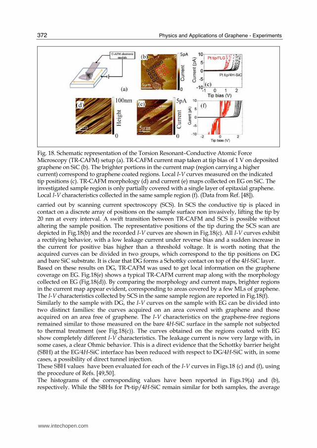
Recently, the properties of the interface between EG and the zero layer have been investigated with nanoscale lateral resolution and compared with those of graphene mechanically exfoliated from HOPG and deposited on 4H-SiC (0001) [48]. In fact, in the case of deposited graphene (DG) no zero layer is present at the interface. EG was grown on n+-doped (0001) 4H-SiC substrate, 8° off axis, with a weakly doped n--epitaxial layer on top, in an inductively heated reactor at a temperature of 2000 °C and under 1 atm Ar pressure [29]. A piece of the same 4H-SiC wafer (not subjected to annealing) was used as the substrate for DG. This local investigation has been performed by measuring the current flowing across the interface using torsion resonance conductive atomic force microscopy (TR-CAFM) and scanning current spectroscopy (SCS). TR-CAFM (see schematic in Fig.18(a)) is a dynamic scanning probe method which allows nondestructive electrical measurements from a conductive tip oscillating in a torsional or twisting mode in close proximity to the sample surface (0.3–3 nm). When a bias is applied between the tip and the sample backside, a map of the current flowing from the tip to sample surface is acquired. This noncontact method has a distinct advantage over the conventional conductive atomic force microscopy performed in contact mode because of the absence of shear forces that can damage the graphene sheets. Commercially available Si n+-doped probes with platinum (Pt) coating were used, with a typical radius of the apex of 10–20 nm. TR-CAFM was used to measure, simultaneously, topographic and current maps on the sample surface. Fig.18(b) shows a TR-CAFM current map taken on DG at tip bias of 1 V. The brighter portions in the current map (region carrying a higher current) correspond to graphene. After identifying the SiC regions coated with DG, local I-V measurements were
www.intechopen.com
Physics and Applications of Graphene - Experiments
372
(d)(d)(d)
Fig. 18. Schematic representation of the Torsion Resonant–Conductive Atomic Force Microscopy (TR-CAFM) setup (a). TR-CAFM current map taken at tip bias of 1 V on deposited graphene on SiC (b). The brighter portions in the current map (region carrying a higher current) correspond to graphene coated regions. Local I-V curves measured on the indicated tip positions (c). TR-CAFM morphology (d) and current (e) maps collected on EG on SiC. The investigated sample region is only partially covered with a single layer of epitaxial graphene. Local I-V characteristics collected in the same sample region (f). (Data from Ref. [48]).
carried out by scanning current spectroscopy (SCS). In SCS the conductive tip is placed in contact on a discrete array of positions on the sample surface non invasively, lifting the tip by 20 nm at every interval. A swift transition between TR-CAFM and SCS is possible without altering the sample position. The representative positions of the tip during the SCS scan are depicted in Fig.18(b) and the recorded I-V curves are shown in Fig.18(c). All I-V curves exhibit a rectifying behavior, with a low leakage current under reverse bias and a sudden increase in the current for positive bias higher than a threshold voltage. It is worth noting that the acquired curves can be divided in two groups, which correspond to the tip positions on DG and bare SiC substrate. It is clear that DG forms a Schottky contact on top of the 4H-SiC layer. Based on these results on DG, TR-CAFM was used to get local information on the graphene coverage on EG. Fig.18(e) shows a typical TR-CAFM current map along with the morphology collected on EG (Fig.18(d)). By comparing the morphology and current maps, brighter regions in the current map appear evident, corresponding to areas covered by a few MLs of graphene. The I-V characteristics collected by SCS in the same sample region are reported in Fig.18(f). Similarly to the sample with DG, the I-V curves on the sample with EG can be divided into two distinct families: the curves acquired on an area covered with graphene and those acquired on an area free of graphene. The I-V characteristics on the graphene-free regions remained similar to those measured on the bare 4H-SiC surface in the sample not subjected to thermal treatment (see Fig.18(c)). The curves obtained on the regions coated with EG show completely different I-V characteristics. The leakage current is now very large with, in some cases, a clear Ohmic behavior. This is a direct evidence that the Schottky barrier height (SBH) at the EG/4H-SiC interface has been reduced with respect to DG/4H-SiC with, in some cases, a possibility of direct tunnel injection. These SBH values have been evaluated for each of the I-V curves in Figs.18 (c) and (f), using the procedure of Refs. [49,50D]. The histograms of the corresponding values have been reported in Figs.19(a) and (b), respectively. While the SBHs for Pt-tip/4H-SiC remain similar for both samples, the average
www.intechopen.com
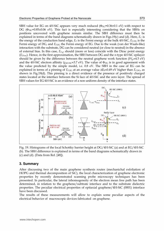
Electronic Properties of Graphene Probed at the Nanoscale
373
SBH value for EG on 4H-SiC appears very much reduced (ΦEG=0.36±0.1 eV) with respect to DG (ΦDG=0.85±0.06 eV). This fact is especially interesting considering that the SBHs on positions uncovered with graphene remain similar. The SBH difference must then be explained in terms of the band diagrams schematically drawn in Figs.19(c) and (d). Here, EC is the energy of the conduction band edge, EF is the Fermi energy at the bulk 4H-SiC, EF,DG is the Fermi energy of DG, and EF,EG the Fermi energy of EG. Due to the weak (van der Waals-like) interaction with the substrate, DG can be considered neutral (or close to neutral) in the absence of external bias. In this case, EF,gr should (more or less) coincide with the Dirac point energy (EDirac). Hence, in the first approximation, the SBH between DG and the n-type 4H-SiC epilayer should be given by the difference between the neutral graphene work function (Wgr≈4.5 eV) and the 4H-SiC electron affinity (χ4H-SiC≈3.7 eV). The value of ΦDG is in good agreement with the value predicted by the simple model, i.e. 0.8 eV. The SBH in the case of EG can be explained in terms of a pinning of EF,EG at an average value ΔEF≈0.49 eV higher than EF,DG, as shown in Fig.19(d). This pinning is a direct evidence of the presence of positively charged states located at the interface between the Si face of 4H-SiC and the zero layer. The spread of SBH values for EG/4H-SiC is an evidence of a non uniform density of the interface states.
Fig. 19. Histograms of the local Schottky barrier height at DG/4H-SiC (a) and at EG/4H-SiC (b). The SBH difference is explained in terms of the band diagrams schematically drawn in (c) and (d). (Data from Ref. [48]).
3. Summary
After discussing two of the main graphene synthesis routes (mechanichal exfoliation of HOPG and thermal decomposition of SiC), the local characterization of graphene electronic properties by recently demonstrated scanning probe microscopy techniques has been presented. In particular, the lateral inhomogeneity of the electron mean free path has been determined, in relation to the graphene/subtrate interface and to the substrate dielectric properties. The peculiar electrical properties of epitaxial graphene/4H-SiC (0001) interface have been discussed. The results of these measurements will allow to explain some peculiar aspects of the electrical behavior of macroscopic devices fabricated on graphene.
www.intechopen.com

Physics and Applications of Graphene - Experiments
374
4. Acknowledgment
This work has been supported, in part, by the European Science Foundation (ESF) under the EUROCORE program EuroGRAPHENE, within GRAPHIC-RF coordinated project.
5. References
[1] Novoselov, K. S.; et al. (2004). Electric Field Effect in Atomically Thin Carbon Films. Science, Vol. 306, pp. 666.
[2] Andreoni, W., 2000, The Physics of Fullerene-Based and Fullerene-Related Materials (Springer, Berlin).
[3] Saito, R., G. Dresselhaus, and M. S. Dresselhaus, 1998, Physical Properties of Carbon Nanotubes, Imperial College Press, London.
[4] Charlier, J.-C.; Blase, X. & S. Roche. (2007). Rev. Mod. Phys. Vol. 79, pp. 677. [5] Novoselov, K. S.; Geim, A. K.; Morozov, S. V.; Jiang, D.; Zhang, Y.; Katsnelson, M. I.;
Grigorieva, I. V.; Dubonos, S. V. & A. A. Firsov. (2005). Two-dimensional gas of massless Dirac fermions in graphene, Nature Vol. 438, pp. 197– 200.
[6] Zhang, Y.; Tan, Y.-W.; Stormer, H. L. & P. Kim. (2005). Experimental observation of the quantum hall effect and Berry’s phase in graphene, Nature Vol. 438, pp. 201–204.
[7] Novoselov, K. S.; Jiang, Z.; Zhang, Y.; Morozov, S. V.; Stormer, H. L.; Zeitler, U.; Maan, J. C.; Boebinger, G. S.; Kim, P.; and & Geim, A. K. (2007). Room-Temperature Quantum Hall Effect in Graphene. Science Vol. 315, pp. 1379–.
[8] Lin, Y.-M.; Dimitrakopoulos, C.; Jenkins, K. A.; Farmer, D. B.; Chiu, H.-Y.; Grill, A.; Avouris, Ph. (2010). 100-GHz Transistors from Wafer-Scale Epitaxial Graphene. Science, Vol. 327, pp. 662.
[9] Wang, X.; Zhi, L.; Tsao, N.; Tomovic, Z.; Li, J.; Mullen, K. (2008). Transparent Carbon Films as Electrodes in Organic Solar Cells. Angew. Chem., Vol. 120, pp. 3032-3034.
[10] Elias, D. C.; Nair, R. R.; Mohiuddin, T. M. G.; Morozov, S. V.; Blake, P.; Halsall, M. P.; Ferrari, A. C.; Boukhvalov, D. W.; Katsnelson, M. I.; Geim, A. K.; Novoselov, K. S. (2009). Control of Graphene's Properties by Reversible Hydrogenation: Evidence for Graphane. Science, Vol. 323, pp. 610-613.
[11] Ni, Z. H.; Yu, T.; Lu, Y. H.; Wang, Y. Y.; Feng, Y. P.; & Shen, Z. X. (2008). Uniaxial Strain on Graphene: Raman Spectroscopy Study and Band-Gap Opening, ACS Nano, Vol. 2, pp. 2301–2305.
[12] Zhang, Y.; Tang, T.-T.; Girit, C.; Hao, Z; Martin, M.C.; Zettl, A.; Crommie, M. F.; Shen, R. Y. & Wang, F. (2009). Direct observation of a widely tunable bandgap in bilayer graphene. Nature Letters, Vol. 459, pp.820-823.
[13] Rotenberg, E.; Bostwick, A.; Ohta, T.; McChesney, J. L.; Seyller, T. & Horn, K. (2008). Origin of the energy bandgap in epitaxial graphene, Nature Materials, Vol. 7, pp. 258 – 259.
[14] Han, M. Y. ; Ozyilmaz, B.; Zhang, Y.; Kim, P. (2007). Energy Band-Gap Engineering of Graphene Nanoribbons. Phys. Rev. Lett. 98, 206805.
[15] Wang, X.; Li, X.; Zhang, L.; Yoon, Y.; Weber, P. K.; Wang, H. & Dai, H. (2009). N-Doping of Graphene Through Electrothermal Reactions with Ammonia. Science, Vol. 324, pp. 768-771.
[16] Lee, E. J. H.; Balusubramanian, K.; Weitz, R. T.; Burghard, M. & Kern, K. (2008). Contact and edge effects in graphene devices. Nat. Nanotechnol. Vol. 3, pp. 486-490.
www.intechopen.com

Electronic Properties of Graphene Probed at the Nanoscale
375
[17] Casiraghi, C.; Pisana, S.; Novoselov, K. S.; Geim, A. K.; & Ferrari, A. C. (2007). Raman fingerprint of charged impurities in graphene. Appl. Phys. Lett. Vol. 91, 233108.
[18] Martin, J.; Akerman, N.; Ulbricht, G.; Lohmann, T.; Smet, J.; Klitzing, K. V. & Yacoby, A. (2008). Observation of electron–hole puddles in graphene using a scanning single-electron transistor. Nature Phys. Vol. 4, pp. 144-148.
[19] Zhang, Y.; Brar, V. W.; Girit, C.; Zett, A.; Crommie, M. F. (2009). Origin of spatial charge inhomogeneity in graphene. Nature Phys. Vol. 5, pp. 722-726.
[20] Hernandez, Y.; Nicolosi, V.; Lotya, M.; Blighe, F. M.; Sun, Z.; De, S.; McGovern, I. T.; Holland, B.; Byrne, M.; Gun'Ko, Y. K.; Boland, J. J.; Niraj, P.; Duesberg, G.; Krishnamurthy, S.; Goodhue, R.; Hutchison, J.; Scardaci, V.; Ferrari, A. C. & Coleman, J. N. (2008). High-yield production of graphene by liquid-phase exfoliation of graphite, Nature Nanotechnology, Vol. 3, pp. 563 - 568.
[21] Li, X.; et al. (2009). Large-Area Synthesis of High-Quality and Uniform Graphene Films on Copper Foils. Science, Vol. 324, pp. 1312.
[22] Lee, Y.; Bae, S.; Jang, H.; Jang, S.; Zhu, S.-E.; Sim, S. H.; Il Song, Y.; Hong, B. H.; Ahn, J.-H. (2010). Wafer-Scale Synthesis and Transfer of Graphene Films, Nano Lett. Vol. 10, pp. 490.
[23] Berger, C.; Song, Z.; Li, X.; Wu, X.; Brown, N.; Naud, C.; Mayou, D.; Li, T.; Hass, J.; Marchenkov, A. N.; Conrad, E. H.; First, P. N. & de Heer, W. A. (2006). Electronic Confinement and Coherence in Patterned Epitaxial Graphene, Science Vol. 312, pp. 1191.
[24] Giannazzo, F.; Sonde, S.; Raineri, V.; Patanè, G.; Compagnini, G.; Aliotta, F.; Ponterio, R.; & Rimini, E. (2010). Optical, morphological and spectroscopic characterization of graphene on SiO2, Phys. Status Solidi C Vol. 7, pp. 1251.
[25] Ferrari, A. C.; Meyer, J. C.; Scardaci, V.; Casiraghi, C.; Lazzeri, M.; Mauri, F.; Piscanec, S.; Jiang, D.; Novoselov, K. S.; Roth, S.; & A. K. Geim. Raman Spectrum of Graphene and Graphene Layers, (2006). Phys. Rev. Lett. Vol. 97, pp. 187401
[26] Blake, P.; Hill, E. W.; Castro Neto, A. H.; Novoselov, K. S.; Jiang, D.; Yang, R.; Booth, T. J.; & Geim, A. K. (2007). Making graphene visible, Appl. Phys. Lett. Vol. 91, pp. 063124.
[27] Nair, R. R.; Blake, P.; Grigorenko, A. N.; Novoselov, K. S.; Booth, T. J.; Stauber, T.; Peres, N. M. R.; Geim, A. K. (2008). Fine Structure Constant Defines Visual Transparency of Graphene. Science Vol. 320, 1308.
[28] Emtsev, K. V.; Bostwick, A.; Horn, K.; Jobst, J.; Kellogg, G. L.; Ley, L.; McChesney, J. L.; Ohta, T.; Reshanov, S. A.; Rohrl, J.; Rotenberg, E.; Schmid, A. K.; Waldmann, D.; Weber, H. B.; & Seyller, T. (2009). Towards wafer-size graphene layers by atmospheric pressure graphitization of SiC(0001). Nature Materials. Vol. 8, pp. 203.
[29] Virojanadara, C.; Syvajarvi, M.; Yakimova, R.; Johansson, L.; Zakharov, I. & T. Balasubramanian. (2008). Homogeneous large-area graphene layer growth on 6H -SiC(0001). Phys. Rev. B Vol. 78, 245403.
[30] Bolen, M. L.; Harrison, S. E.; Biedermann, L. B.; & Capano, M. A. (2009). Graphene formation mechanisms on 4H-SiC(0001). Phys. Rev. B Vol. 80, pp. 115433.
[31] Vecchio, C.; Giannazzo, F.; Sonde, S. ; Bongiorno, C. ; Rambach, M.; Yakimova, R.; Rimini, E.; Raineri, V. (2010). Nanoscale structural characterization of epitaxial graphene grown on off-axis 4H-SiC (0001). Nanoscale Research Letters, in press.
[32] Prakash, G.; Capano, M. A.; Bolen, M. L.; Zemlyanov, D.; Reifenberger, R. G. (2010). AFM study of ridges in few-layer epitaxial graphene grown on the carbon-face of 4H–SiC (000-1). Carbon. Vol. 48, pp. 2383-2393.
www.intechopen.com

Physics and Applications of Graphene - Experiments
376
[33] Sun, G. F.; Jia, J. F.; Xue, Q. K. & Li, L. (2009). Atomic-scale imaging and manipulation of ridges on epitaxial graphene on 6H-SiC(0001). Nanotechnology, Vol. 20, pp. 355701.
[34] Chen, J.H.; Jang, C.; Xiao, S.; Ishigami, M. & Fuhrer, M.S. (2008). Intrinsic and extrinsic performance limits of graphene devices on SiO2. Nature Nanotechnology, Vol. 3, pp. 206-209.
[35] Bolotin, K. I.; Sikes, K. J.; Jiang, Z.; Klima, M.; Fudenberg, G.; Hone, J.; Kim P. & Stormer, H. L. (2008). Ultrahigh electron mobility in suspended graphene. Solid State Commun. Vol. 146, pp. 351-355.
[36] Hwang, E. H.; Adam, S.; & Das Sarma, S. (2007). Carrier Transport in Two-Dimensional Graphene Layers. Phys. Rev. Lett. Vol. 98, pp. 186806.
[37] Fratini, S.; & Guinea, F. (2008). Substrate-limited electron dynamics in graphene. Phys. Rev. B Vol. 77, pp. 195415.
[38] Giannazzo, F.; Sonde, S.; Raineri, V.; & Rimini, E. (2009). Irradiation damage in graphene on SiO2 probed by local mobility measurements, Appl. Phys. Lett. Vol. 95, pp. 263109.
[39] Giannazzo, F.; Sonde, S.; Rimini, E. & Raineri, V. (2010). Lateral homogeneity of the electronic properties in pristine and ion irradiated graphene probed by scanning capacitance spectroscopy, Nanoscale Research Letters, in press.
[40] Giannazzo, F., Sonde, S., Raineri, V., & Rimini, E. (2009). Screening Length and Quantum Capacitance in Graphene by Scanning Probe Microscopy. Nano Letters Vol. 9, pp. 23
[41] Sonde, S.; Giannazzo, F.; Raineri, V.; & Rimini, E. (2009). Dielectric thickness dependence of capacitive behavior in graphene deposited on silicon dioxide. J. Vac. Sci. Technol. B. Vol. 27, pp. 868
[42] Rutter, G. M.; Crain, J. N.; Guisinger, N. P.; Li, T.; First, P. N.; & Stroscio, J. A. (2007). Scattering and Interference in Epitaxial Graphene. Science .Vol. 317, 219-222.
[43] Sonde, S.; Giannazzo, F.; Vecchio, C.; Yakimova, R.; Rimini, E.; & Raineri, V. (2010). Role of graphene/substrate interface on the local transport properties of the two-dimensional electron gas, Appl. Phys. Lett. Vol. 97, pp. 132101
[44] Stauber, T.; Peres, N. M. R.; & Guinea, F. (2007). Electronic transport in graphene: A semiclassical approach including midgap states, Phys. Rev. B Vol. 76, pp. 205423
[45] Perebeinos, V.; & Avouris, Ph. (2010). Inelastic scattering and current saturation in graphene, Phys. Rev. B Vol. 81, pp. 195442.
[46] Wang, S. Q.; & Mahan, G. D. (1972). Electron Scattering from Surface Excitations. Phys. Rev. B. Vol. 6, pp. 4517-4524.
[47] Emtsev, K. V.; Speck, F.; Seyller, Th.; Ley, L.; Riley, J. D. (2008). Interaction, growth, and ordering of epitaxial graphene on SiC{0001} surfaces: A comparative photoelectron spectroscopy study. Phys. Rev. B Vol. 77, pp. 155303.
[48] Sonde, S.; Giannazzo, F.; Raineri, V.; Yakimova, R.; Huntzinger, J.-R.; Tiberj, A. & Camassel, J. (2009). Electrical properties of the graphene/4H-SiC (0001) interface probed by scanning current spectroscopy, Phys. Rev. B Vol. 80, pp. 241406(R).
[49] Giannazzo, F.; Roccaforte, F.; Raineri, V. & Liotta, S. F. (2006). Transport localization in heterogeneous Schottky barriers of quantum-defined metal films, EuroPhysics Letters Vol. 74, pp. 686.
[50] Giannazzo, F.; Roccaforte, F.; Iucolano, F.; Raineri, V.; Ruffino, F. & Grimaldi, M. G. (2009). Nanoscale current transport through Schottky contacts on wide bandgap semiconductors, J. Vac. Sci. Technol. B 27, pp. 789.
www.intechopen.com
Physics and Applications of Graphene - ExperimentsEdited by Dr. Sergey Mikhailov
ISBN 978-953-307-217-3Hard cover, 540 pagesPublisher InTechPublished online 19, April, 2011Published in print edition April, 2011
InTech EuropeUniversity Campus STeP Ri Slavka Krautzeka 83/A 51000 Rijeka, Croatia Phone: +385 (51) 770 447 Fax: +385 (51) 686 166www.intechopen.com
InTech ChinaUnit 405, Office Block, Hotel Equatorial Shanghai No.65, Yan An Road (West), Shanghai, 200040, China
Phone: +86-21-62489820 Fax: +86-21-62489821
The Stone Age, the Bronze Age, the Iron Age... Every global epoch in the history of the mankind ischaracterized by materials used in it. In 2004 a new era in material science was opened: the era of grapheneor, more generally, of two-dimensional materials. Graphene is the strongest and the most stretchable knownmaterial, it has the record thermal conductivity and the very high mobility of charge carriers. It demonstratesmany interesting fundamental physical effects and promises a lot of applications, among which are conductiveink, terahertz transistors, ultrafast photodetectors and bendable touch screens. In 2010 Andre Geim andKonstantin Novoselov were awarded the Nobel Prize in Physics "for groundbreaking experiments regarding thetwo-dimensional material graphene". The two volumes Physics and Applications of Graphene - Experimentsand Physics and Applications of Graphene - Theory contain a collection of research articles reporting ondifferent aspects of experimental and theoretical studies of this new material.
How to referenceIn order to correctly reference this scholarly work, feel free to copy and paste the following:
Filippo Giannazzo, Sushant Sonde and Vito Raineri (2011). Electronic Properties of Graphene Probed at theNanoscale, Physics and Applications of Graphene - Experiments, Dr. Sergey Mikhailov (Ed.), ISBN: 978-953-307-217-3, InTech, Available from: http://www.intechopen.com/books/physics-and-applications-of-graphene-experiments/electronic-properties-of-graphene-probed-at-the-nanoscale

© 2011 The Author(s). Licensee IntechOpen. This chapter is distributedunder the terms of the Creative Commons Attribution-NonCommercial-ShareAlike-3.0 License, which permits use, distribution and reproduction fornon-commercial purposes, provided the original is properly cited andderivative works building on this content are distributed under the samelicense.