Embed Size (px)
Citation preview
PHYSICAL REVIEW B 94, 195155 (2016)
Electronic structure and magnetism of strained bcc phases acrossthe fcc to bcc transition in ultrathin Fe films
Alberto Calloni,1,* Giulia Berti,1 Gianlorenzo Bussetti,1 Guido Fratesi,2 Marco Finazzi,1 Franco Ciccacci,1 and Lamberto Duo1
1Dipartimento di Fisica, Politecnico di Milano, Piazza Leonardo Da Vinci, 32, 20133 Milano, Italy2ETSF, CNISM, Dipartimento di Fisica, Universita degli Studi di Milano, via Celoria 16, I-20133 Milano, Italy
(Received 24 September 2016; published 30 November 2016)
We investigated the electronic structure of the bcc metastable phases involved in the fcc to bcc transitionof Fe. Ultrathin Fe films were grown on a 2-monolayer (ML) Ni/W(110) substrate, where a fcc lattice isstabilized at low Fe coverages and the transition proceeds through the formation of bcc nuclei showing a specific“Kurdjumov-Sachs” orientation with the substrate. A comprehensive description of the electronic structureevolution is achieved by combining spin-resolved UV photoemission spectroscopy and ab initio calculations.According to our results, an exchange-split band structure is observed starting from 2 ML of Fe, concomitantwith the formation of ferromagnetic bcc nuclei. Continuous modifications are observed in the spin-resolvedphotoemission spectra for increasing Fe coverage, especially for what concerns the minority states, possiblyindicative of the progressive relaxation of the strained bcc phase starting from the bcc/fcc interface.
DOI: 10.1103/PhysRevB.94.195155
I. INTRODUCTION
The present work focuses on the electronic and magneticproperties of ultrathin, epitaxial Fe films. In standard con-ditions of temperature and pressure (273 K and 100 kPa),bulk Fe shows a bcc, ferromagnetic crystal structure, calledthe α phase [1]. Unstable Fe phases, such as fcc γ -Fe(austenite), can be realized in very thin films grown on propermaterials, typically with a fcc crystal structure, where Fe atomsare forced to adopt the same atomic arrangement of thesubstrate (pseudomorphic growth). As a consequence of theloading of elastic energy in the films, at larger thicknesses Feinvariably relaxes towards its bulk configuration. According tothe literature [2,3], this is likely to occur through a diffusionlessphase transformation, called a martensitic transformation.In principle, the fully relaxed bcc bulk structure can beobtained from the fcc one by applying a continuous tetragonaldeformation of the unit cell (the so-called Bain strain). Inpractice, more complicated atomic displacements are observedfollowing, e.g., the so-called Nishiyama-Wassermann (NW)or Kurdjumov-Sachs (KS) pathways [2]. Being a first-orderphase transformation, the martensitic transformation impliesthe formation and evolution of bcc nuclei within a fcc host.The bcc nuclei are usually strained and then undergo a gradualrelaxation towards the bulk equilibrium structure [4]. In someparticular systems, the relaxation is more abrupt and thestrained nuclei can be even considered as an intermediate orprecursor phase within the martensitic transformation [5].
Historically, the research on thin Fe films focused on thestudy of the Fe fcc phase, which might be characterized,owing to its low dimensionality and crystal structure, bya ferromagnetic behavior with enhanced magnetic moments[6–8].The stabilization and the determination of the magneticbehavior of such phase, however, proved to be a formidabletask. The use of different substrates (with different latticeparameters and surface crystallographic orientation) and dif-ferent growth methodologies (molecular beam epitaxy either
at cryogenic substrate temperature or at room temperaturevs pulsed laser deposition or electrochemical deposition),for instance, gave rise to a complex phenomenology [9–11].One-layer-thick Fe films [or Fe monolayers (ML)] on not-magnetic fcc (hcp) substrates such as Cu [12] or Ir (Ru) [13],are characterized either by an antiferromagnetic ordering,or a rather complex noncollinear arrangement of the localmagnetic moments [14], while a paramagnetic behavior hasbeen reported for Au [15]. Thicker Fe films have been alsoinvestigated, the most known example being Fe on Cu(001)for Fe thicknesses in the 5–10 ML range, which shows apeculiar behavior with a ferromagnetic top bilayer sitting onan antiferromagnetic bulk [16,17]. One major complicationto the complete understanding of the magnetic behavior ofthin films is, however, the magnetic response of the bccphase. Past investigations with averaging techniques such asphotoemission spectroscopy (PES) or magneto-optical Kerreffect (MOKE), for instance, detected a not-nil magnetic signalon thin Fe films and related it to the appearance of either low- orhigh-spin ferromagnetic γ (i.e., fcc) phases [18,19]. However,accurate structural studies performed by scanning tunnelingmicroscopy revealed, also in those cases, the formation ofbcc nuclei, calling for a more complex interpretation of theprevious experimental results (see, for instance, the ongoingdiscussion on the growth of Fe on Cu(001) [20,21] orCu(111) [3]). Our goal is, therefore, to improve, by meansof electron spectroscopies, and also with spin resolution, thepresent understanding of the electronic and magnetic structureof thin Fe films, starting from a more accurate investigation ofthe spectroscopic signal which is expected from the fcc phaseand from the bcc nuclei, and from an assessment of the overallsensitivity of averaging techniques such as PES to the onset ofthe phase transformation. From a slightly different perspective,we foresee a contribution from such investigation also to theunderstanding of the electronic structure of Fe films where adistorted lattice is “stabilized” by means of alloying. Orderedalloys of, e.g., FePt [22] or FeCo [23] are notable examples.In those cases, characterized by the tetragonal distortion of thebcc Fe unit cell, a ferromagnetic behavior is obtained, togetherwith a high uniaxial magnetocrystalline anisotropy, usually in
2469-9950/2016/94(19)/195155(11) 195155-1 ©2016 American Physical Society
ALBERTO CALLONI et al. PHYSICAL REVIEW B 94, 195155 (2016)
the direction perpendicular to the film plane. Such systemsare currently being researched for applications in magneticand magneto-optical recording [24] and in spintronic devicessuch as magnetic random access memories (MRAMs) [25].Recently, the study reported in Ref. [26] has shown thefeasibility of an irradiation-induced fcc to bcc transformationin thick, nonmagnetic fcc Fe films alloyed with Ni thatwould allow, in perspective, for the magnetic patterning ofa metastable Fe substrate by focused ion or electron beams.
In the present study, a well-defined crystallographic struc-ture is obtained for the Fe films by following the strategy ofRef. [2]. Instead of the well-investigated (but still problematic)Cu, we chose a Ni substrate for our electronic and magneticcharacterization. Although the Cu lattice parameter is closerto that characteristic of γ -Fe (3.52 A) [1], the lattice mismatchin the Ni case is tolerable (below 3%) and, more important, thegrowth of Fe produces a much more controlled morphology(i.e., a nearly layer-by-layer growth at low coverages), thanksto a negligible Fe/Ni interdiffusion, even at room temperature(RT) [2,27], and similar surface energies [28]. Magnetic biasfrom Ni is reduced by using ultrathin Ni films. In particular, weused a 2-ML Ni/W(110) multilayer structure. As it will becomeapparent in the following, the choice of a bcc substrate (W inthe present case) is not accidental: while it does not preventthe formation of a fcc Ni surface [29], it steers the fcc to bcctransformation of Fe by selecting fewer bcc variants, thereforesimplifying the interpretation of the experimental results.
The paper is organized as follows. After a description of themethods in Sec. II, we present our results in Sec. III: in the firstpart, the morphological evolution of the Fe surface is describedby means of low-energy electron diffraction (LEED). Theelectronic structure is then investigated by means of spin-resolved photoemission spectroscopy (SRPES). Eventually, inSec. IV the results are discussed in light of (i) the availableinformation on bulk Fe and (ii) ab initio calculations devisedto link the observed evolution to the structural modificationsoccurring within the bcc phase.
II. METHODS
A. Growth and spectroscopic characterization
Our measurements were performed in an ultrahigh-vacuum(UHV) system with a base pressure in the low 10–8 Parange [30]. The W(110) single crystal (MaTecK GmbH)was cleaned according to standard procedures [31,32], whichinvolved heating in an O2 atmosphere in order to desorb segre-gated carbon and flashing at 2300 K in UHV. The concentrationof surface contaminants was below the sensitivity of our x-rayphotoemission spectroscopy (XPS) characterization. A highquality of the tungsten surface was inferred from a sharp(1×1) LEED pattern and from the detection of surface relatedfeatures with PES (see Ref. [33]). Electron-beam heating wasused to sublimate Ni and Fe from high-purity (5N) rods.The Ni and Fe deposition rates were previously calibratedusing an oscillating quartz microbalance and were kept below2.0 ML/min, 1 ML being a single atomic layer referred to thefcc (111) surface, with a thickness of 2.03 and 2.19 A for Ni andFe, respectively [2]. Following the literature [34], we applieda two-step procedure for the Ni growth: (i) the W crystal was
kept at 570 K during the growth of the first Ni monolayer inorder to favor the Ni atom mobility on the substrate and obtaina flat morphology; (ii) the substrate was then kept at roomtemperature (RT) for further Ni and Fe depositions. Duringthe growth of the metallic films the pressure in the UHVchamber remained in the 10−8 Pa range. After the growth, eachsample was analyzed by LEED and XPS at RT. Samples weremagnetized in situ (either at RT or at cryogenic temperature,down to 30 K) by applying a pulsed magnetic field of 2200 Oealong the [001] direction of the W substrate and analyzed atmagnetic remanence. The temperature was set by means ofa closed-cycle He cryostat accurately calibrated by replacingthe sample with a silicon diode sensor. PES was performedby exciting electrons with He I or He II radiation ( hν = 21.2and 40.8 eV, respectively) and detecting them by means of a150-mm hemispherical analyzer (from SPECS GmbH) withan angular resolution of ±1◦. Spin-resolved (SR) spectra wereacquired by means of a micro-Mott detector [35], mounted atthe exit side of the hemispherical analyzer. Typical full widthat half maximum (FWHM) energy resolution values are 15and 120 meV for PES and SRPES, respectively. The data wereacquired at cryogenic temperature (30 K).
B. Ab initio calculations
We performed ab initio density functional theory (DFT)simulations by taking the generalized gradient approximationto the exchange and correlation functional as proposed byPerdew, Burke, and Ernzerhof (GGA PBE) [36]. The QUAN-TUM ESPRESSO package [37] was used for the calculations,within plane waves and ultrasoft pseudopotentials. The Fepseudopotential was generated starting from scalar-relativisticall-electron atomic calculations and using nonlinear corecorrections, and has been extensively studied in our previousworks [38–40]. We used a kinetic energy cutoff of 45 Ry for thewave functions and 200 Ry for the effective potential and thecharge density. We considered for the bulk bcc Fe lattice a con-ventional orthorhombic cell with the x,y, and z axes orientedalong [001], [110], and [110], respectively, and a bulk latticeparameter of 2.83 A. For that cell we have taken a 14 × 10 ×10 sampling of the Brillouin zone. Additionally, the computedbands have been projected on a complete set of d-like atomicorbitals, oriented according to the x,y, z directions of the or-thorhombic cell. This unit cell was the starting point to simulateFe structural deformations as will be detailed in Sec. IV.
III. RESULTS
A. Morphological evolution
All samples were bilayers comprised of a thin Ni “buffer”layer with a nominal thickness of 2 ML, grown on aW(110) substrate, and a Fe layer with variable thickness(ranging from 2 to 40 ML). Consistent with the literature,we observe for the buffer layer (not shown) a fcc atomicarrangement already from the first monolayer, exposing theNi(111) surface. The Ni lattice is aligned to the substrateaccording to the NW relationship, W[001]bcc ‖ Ni[110]fcc andW[110]bcc ‖ Ni[112]fcc. The strain of the Ni film is minimalin the W[110] direction (about 3%), while in the W[001]direction the Ni layer relaxes and a coincidence structure is
195155-2
ELECTRONIC STRUCTURE AND MAGNETISM OF . . . PHYSICAL REVIEW B 94, 195155 (2016)
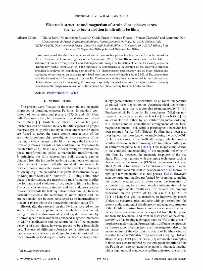
FIG. 1. LEED patterns for increasing Fe coverages on 2-ML Ni/W(110). The electron beam energy is 163 eV. In the insets: closeup ofthe diffraction pattern observed near the (11) fcc spot. The beam energy selected for the insets is 125 eV. The schematic of panel (d) showsthe LEED pattern expected from a bcc surface reconstructed according to the KS relation with white and gray dots, superimposed on the fccpattern of Ni(111) (black dots). Gray dots single out only two of the six equivalent KS domains, thus reproducing the experimental pattern ofpanel (b). The red rectangle shows the bcc Fe(110) primitive cell, rotated by α = 54.8◦ with respect to the W[110] direction.
formed, where nine Ni cells are matched to seven W cells. Thecoincidence structure (also called the 7 × 1 structure) givesrise to a series of bright LEED satellite spots aligned in theW[001] direction. These results, concerning the Ni/W(110)substrate, are in nice agreement with the available literatureand have been discussed in Ref. [41].
In the following, we will focus on the growth of theFe film. Figure 1 shows some characteristic LEED patternsacquired at selected Fe coverages. For coverages ranging fromsubmonolayer up to about 4 ML [Fig. 1(a)], we observed ahexagonal pattern, practically coincident with the Ni(111) one.Faint extra spots, related to the underlying 7 × 1 coincidencestructure, are still visible at the early stages of Fe growth [see,e.g., the inset of Fig. 1(a)]. For coverages larger than about4 ML [Fig. 1(b)], a different pattern is found, characterizedby diffraction spots aligned along the W[110] direction. Thispattern is due to the superposition of the diffraction signalfrom the fcc layers and a bcc (110) surface, aligned accordingto the KS relation. As shown in the schematics of Fig. 1(d),a total of six equivalent KS domains are expected allowingfor a nearly perfect lattice matching (within less than 1%)along the 〈110〉fcc and 〈111〉bcc directions. Due to the strainloaded into the Ni substrate, only two of those domains arestabilized at low Fe coverages, with the bcc Fe(110) unit celltilted with respect to the W(110) surface lattice. Consistentwith the findings of Ref. [2], the angle α is seen to slightlydeviate from the value expected from bulk Fe (54.8°), being,for instance, about 56 ± 1° for the 6-ML sample of Fig. 1(b).
At larger coverages (�8 ML), the LEED pattern appearsblurred and more symmetric with respect to threefold rotationsaround the W[110] axis. The diffraction spots also changefrom round to crescent shaped [see, e.g., the inset of Fig. 1(c)].Our interpretation is that now all KS domains are observed,although still with unequal intensity. This KS-like patternpersists up to 40 Fe ML, i.e., the largest film thickness exploredin the present study. Good agreement is found with the previousLEED and Auger study of Ref. [2] where, however, theformation of a single-domain NW reconstruction is reportedfor thicker Fe layers.1 We attribute such different behaviorto the slightly lower substrate temperature (RT vs 350 K),and possibly to slight differences in the preparation and/orthickness of the buffer layer. It should be stressed, however, thatthe differences between the LEED patterns related to the KSand the NW superstructures can be hardly distinguished in thecase of blurred diffraction spots. The simultaneous presenceof KS and NW domains at large Fe coverages (reported, forinstance, also for the growth of Fe on Au(111) [42]) can beneither confirmed nor ruled out from our data. If thicker Nibuffer layers are used, we clearly observe the formation ofthreefold symmetric NW domains even at small Fe coverages(not shown), in agreement with the available literature on theFe growth on bulk Ni(111) [43,44].
1The NW pattern described in Ref. [2] is retrieved by rotating thered rectangle of Fig. 1(d) in order to reach the condition α = 0◦.
195155-3
ALBERTO CALLONI et al. PHYSICAL REVIEW B 94, 195155 (2016)
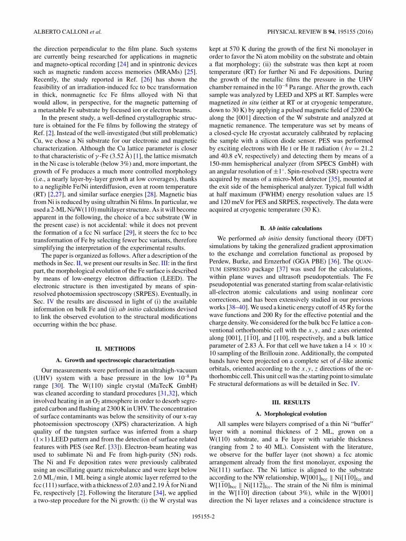
FIG. 2. Photoemission spectra for the 2-ML Ni/W(110) substrate(red line) and for selected Fe coverages (�Fe, black lines). The spectrawere acquired at normal photoelectron emission, with the substratekept at 30 K. He I radiation was used for all but the top spectrum (opendots), acquired with He II radiation. Source satellites were subtractedfrom the He I spectra. Capital letters mark the position of the relevantfeatures discussed in the text: A′ (1-1.4 eV), B′ (0.6 eV), A (0.7 eV),B (0.3 eV), and C close to EF.
B. Electronic structure evolution
Figure 2 shows a series of spin-integrated spectra takenat normal photoelectron emission for increasing Fe coverage.A substrate temperature of about 30 K was chosen for ourcharacterization, resulting in sharper line shapes close to theFermi energy (EF). A small reduction to the overall spectrallinewidth is also expected at larger binding energy (BE) fromthe reduced phonon scattering [45].2 Photoemission from theNi film is characterized by a peak (B′) and a shoulder (A′),the latter partially overlapping with the features related tophotoemission from W 4f orbitals at a binding energy ofabout 1.7 eV (see Ref. [41] for further details). The 2-ML Fespectrum is similar to the Ni one, excepted for a slight shiftof about 0.1 eV of the main photoemission feature, labeledA, that we assign to photoemission from the Fe electronicstates. At larger coverages, a continuous evolution is observed,with the development of peak B at smaller BE and a generalsharpening of the photoemission line shapes. Feature C isrelated to photoemission from an electronic state located at orslightly below EF, which proved itself to be resilient to surface
2A contribution of about 50 meV FWHM is expected at RT for Fe,according to the formula of Ref. [65].
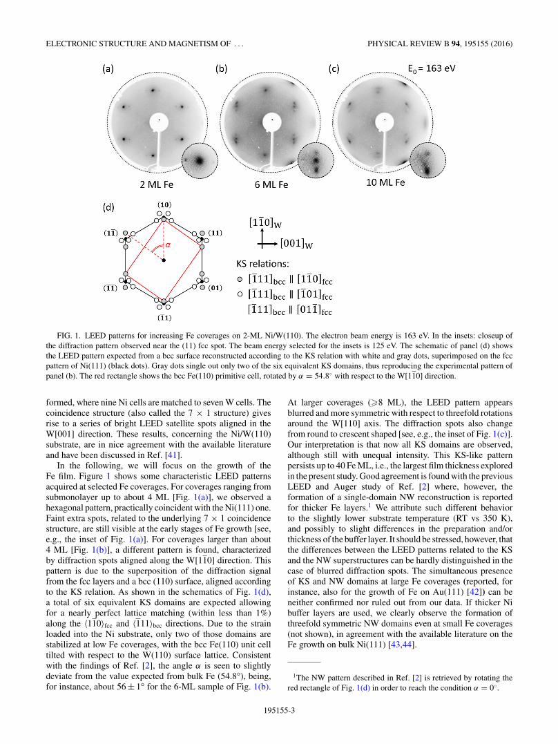
FIG. 3. Spin-resolved photoemission spectra for selected Fecoverages on 2-ML Ni/W(110). Black dots: spin-integrated spectra.Blue and red triangles: photoemission signal I↑↓ from majorityand minority (with respect to the magnetization direction) elec-trons. Green dots: degree of the photoelectrons’ spin polarizationP = (I↑ − I↓)/(I↑ + I↓), retrieved by correcting the measured spinasymmetry by the Sherman function of the detector (S = 0.14,according to our previous calibration [30]). Two sets of spectra wereacquired at normal photoelectron emission, with the substrate keptat 30 K and magnetized along two opposite directions, in order tocancel out any instrumental asymmetry [30,46]. He I radiation wasused and source satellites subtracted.
modification by oxygen (up to 4 L of O2 dosed at RT, where1 L = 10−6 Torr × s). Furthermore, its intensity is stronglymodified by changing the excitation energy from He I to He II
(open dots in Fig. 2), i.e., by changing the region in the bulk
195155-4
ELECTRONIC STRUCTURE AND MAGNETISM OF . . . PHYSICAL REVIEW B 94, 195155 (2016)
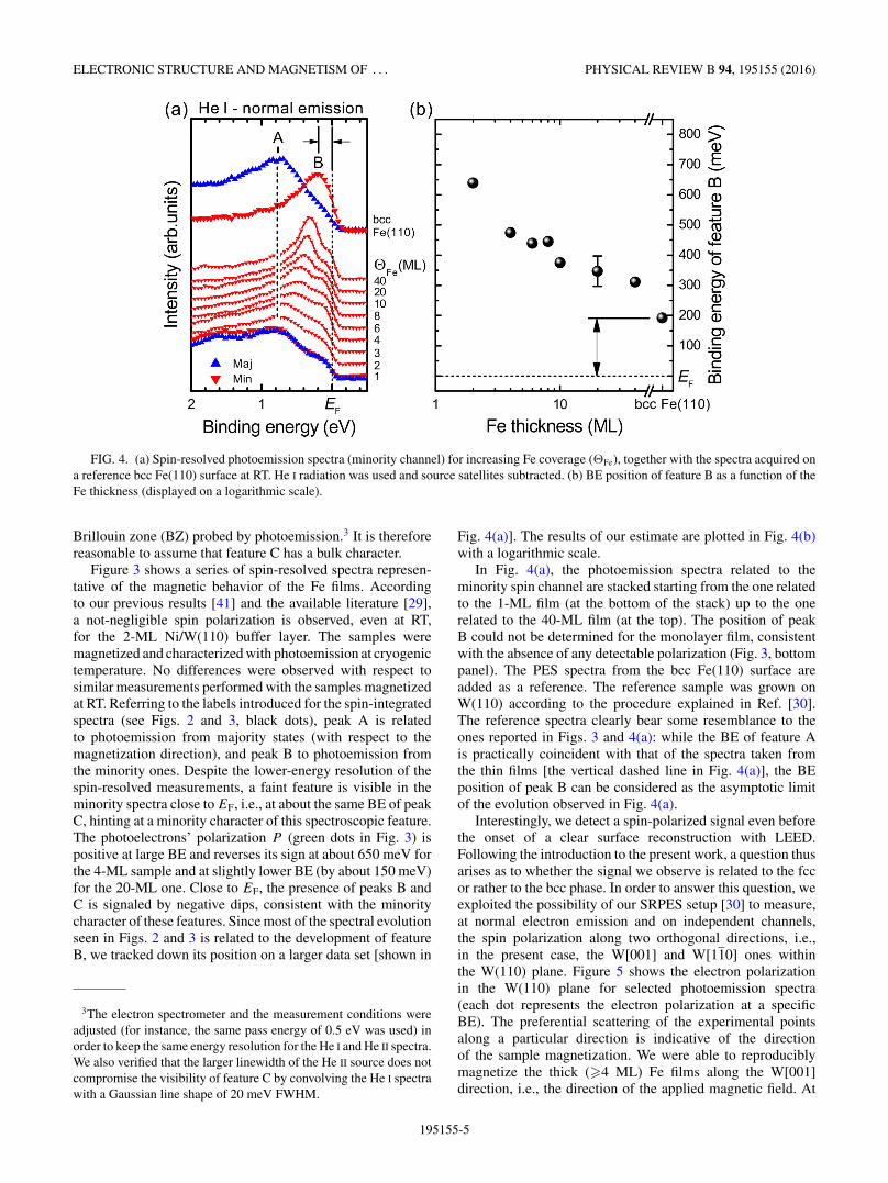
FIG. 4. (a) Spin-resolved photoemission spectra (minority channel) for increasing Fe coverage (�Fe), together with the spectra acquired ona reference bcc Fe(110) surface at RT. He I radiation was used and source satellites subtracted. (b) BE position of feature B as a function of theFe thickness (displayed on a logarithmic scale).
Brillouin zone (BZ) probed by photoemission.3 It is thereforereasonable to assume that feature C has a bulk character.
Figure 3 shows a series of spin-resolved spectra represen-tative of the magnetic behavior of the Fe films. Accordingto our previous results [41] and the available literature [29],a not-negligible spin polarization is observed, even at RT,for the 2-ML Ni/W(110) buffer layer. The samples weremagnetized and characterized with photoemission at cryogenictemperature. No differences were observed with respect tosimilar measurements performed with the samples magnetizedat RT. Referring to the labels introduced for the spin-integratedspectra (see Figs. 2 and 3, black dots), peak A is relatedto photoemission from majority states (with respect to themagnetization direction), and peak B to photoemission fromthe minority ones. Despite the lower-energy resolution of thespin-resolved measurements, a faint feature is visible in theminority spectra close to EF, i.e., at about the same BE of peakC, hinting at a minority character of this spectroscopic feature.The photoelectrons’ polarization P (green dots in Fig. 3) ispositive at large BE and reverses its sign at about 650 meV forthe 4-ML sample and at slightly lower BE (by about 150 meV)for the 20-ML one. Close to EF, the presence of peaks B andC is signaled by negative dips, consistent with the minoritycharacter of these features. Since most of the spectral evolutionseen in Figs. 2 and 3 is related to the development of featureB, we tracked down its position on a larger data set [shown in
3The electron spectrometer and the measurement conditions wereadjusted (for instance, the same pass energy of 0.5 eV was used) inorder to keep the same energy resolution for the He I and He II spectra.We also verified that the larger linewidth of the He II source does notcompromise the visibility of feature C by convolving the He I spectrawith a Gaussian line shape of 20 meV FWHM.
Fig. 4(a)]. The results of our estimate are plotted in Fig. 4(b)with a logarithmic scale.
In Fig. 4(a), the photoemission spectra related to theminority spin channel are stacked starting from the one relatedto the 1-ML film (at the bottom of the stack) up to the onerelated to the 40-ML film (at the top). The position of peakB could not be determined for the monolayer film, consistentwith the absence of any detectable polarization (Fig. 3, bottompanel). The PES spectra from the bcc Fe(110) surface areadded as a reference. The reference sample was grown onW(110) according to the procedure explained in Ref. [30].The reference spectra clearly bear some resemblance to theones reported in Figs. 3 and 4(a): while the BE of feature Ais practically coincident with that of the spectra taken fromthe thin films [the vertical dashed line in Fig. 4(a)], the BEposition of peak B can be considered as the asymptotic limitof the evolution observed in Fig. 4(a).
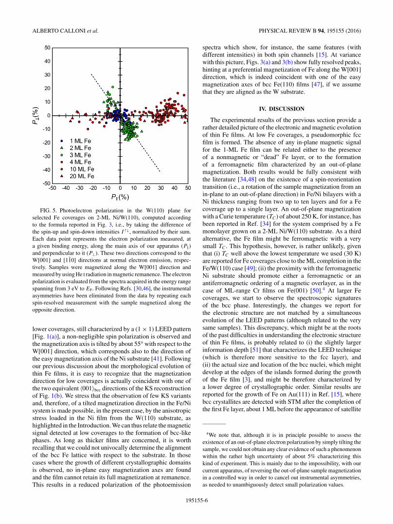
Interestingly, we detect a spin-polarized signal even beforethe onset of a clear surface reconstruction with LEED.Following the introduction to the present work, a question thusarises as to whether the signal we observe is related to the fccor rather to the bcc phase. In order to answer this question, weexploited the possibility of our SRPES setup [30] to measure,at normal electron emission and on independent channels,the spin polarization along two orthogonal directions, i.e.,in the present case, the W[001] and W[110] ones withinthe W(110) plane. Figure 5 shows the electron polarizationin the W(110) plane for selected photoemission spectra(each dot represents the electron polarization at a specificBE). The preferential scattering of the experimental pointsalong a particular direction is indicative of the directionof the sample magnetization. We were able to reproduciblymagnetize the thick (�4 ML) Fe films along the W[001]direction, i.e., the direction of the applied magnetic field. At
195155-5
ALBERTO CALLONI et al. PHYSICAL REVIEW B 94, 195155 (2016)
FIG. 5. Photoelectron polarization in the W(110) plane forselected Fe coverages on 2-ML Ni/W(110), computed accordingto the formula reported in Fig. 3, i.e., by taking the difference ofthe spin-up and spin-down intensities I↑↓, normalized by their sum.Each data point represents the electron polarization measured, ata given binding energy, along the main axis of our apparatus (P‖)and perpendicular to it (P⊥). These two directions correspond to theW[001] and [110] directions at normal electron emission, respec-tively. Samples were magnetized along the W[001] direction andmeasured by using He I radiation in magnetic remanence. The electronpolarization is evaluated from the spectra acquired in the energy rangespanning from 3 eV to EF. Following Refs. [30,46], the instrumentalasymmetries have been eliminated from the data by repeating eachspin-resolved measurement with the sample magnetized along theopposite direction.
lower coverages, still characterized by a (1 × 1) LEED pattern[Fig. 1(a)], a non-negligible spin polarization is observed andthe magnetization axis is tilted by about 55°with respect to theW[001] direction, which corresponds also to the direction ofthe easy magnetization axis of the Ni substrate [41]. Followingour previous discussion about the morphological evolution ofthin Fe films, it is easy to recognize that the magnetizationdirection for low coverages is actually coincident with one ofthe two equivalent 〈001〉bcc directions of the KS reconstructionof Fig. 1(b). We stress that the observation of few KS variantsand, therefore, of a tilted magnetization direction in the Fe/Nisystem is made possible, in the present case, by the anisotropicstress loaded in the Ni film from the W(110) substrate, ashighlighted in the Introduction. We can thus relate the magneticsignal detected at low coverages to the formation of bcc-likephases. As long as thicker films are concerned, it is worthrecalling that we could not univocally determine the alignmentof the bcc Fe lattice with respect to the substrate. In thosecases where the growth of different crystallographic domainsis observed, no in-plane easy magnetization axes are foundand the film cannot retain its full magnetization at remanence.This results in a reduced polarization of the photoemission
spectra which show, for instance, the same features (withdifferent intensities) in both spin channels [15]. At variancewith this picture, Figs. 3(a) and 3(b) show fully resolved peaks,hinting at a preferential magnetization of Fe along the W[001]direction, which is indeed coincident with one of the easymagnetization axes of bcc Fe(110) films [47], if we assumethat they are aligned as the W substrate.
IV. DISCUSSION
The experimental results of the previous section provide arather detailed picture of the electronic and magnetic evolutionof thin Fe films. At low Fe coverages, a pseudomorphic fccfilm is formed. The absence of any in-plane magnetic signalfor the 1-ML Fe film can be related either to the presenceof a nonmagnetic or “dead” Fe layer, or to the formationof a ferromagnetic film characterized by an out-of-planemagnetization. Both results would be fully consistent withthe literature [34,48] on the existence of a spin-reorientationtransition (i.e., a rotation of the sample magnetization from anin-plane to an out-of-plane direction) in Fe/Ni bilayers with aNi thickness ranging from two up to ten layers and for a Fecoverage up to a single layer. An out-of-plane magnetizationwith a Curie temperature (TC) of about 250 K, for instance, hasbeen reported in Ref. [34] for the system comprised by a Femonolayer grown on a 2-ML Ni/W(110) substrate. As a thirdalternative, the Fe film might be ferromagnetic with a verysmall TC . This hypothesis, however, is rather unlikely, giventhat (i) TC well above the lowest temperature we used (30 K)are reported for Fe coverages close to the ML completion in theFe/W(110) case [49]; (ii) the proximity with the ferromagneticNi substrate should promote either a ferromagnetic or anantiferromagnetic ordering of a magnetic overlayer, as in thecase of ML-range Cr films on Fe(001) [50].4 At larger Fecoverages, we start to observe the spectroscopic signaturesof the bcc phase. Interestingly, the changes we report forthe electronic structure are not matched by a simultaneousevolution of the LEED patterns (although related to the verysame samples). This discrepancy, which might be at the rootsof the past difficulties in understanding the electronic structureof thin Fe films, is probably related to (i) the slightly largerinformation depth [51] that characterizes the LEED technique(which is therefore more sensitive to the fcc layer), and(ii) the actual size and location of the bcc nuclei, which mightdevelop at the edges of the islands formed during the growthof the Fe film [3], and might be therefore characterized bya lower degree of crystallographic order. Similar results arereported for the growth of Fe on Au(111) in Ref. [15], wherebcc crystallites are detected with STM after the completion ofthe first Fe layer, about 1 ML before the appearance of satellite
4We note that, although it is in principle possible to assess theexistence of an out-of-plane electron polarization by simply tilting thesample, we could not obtain any clear evidence of such a phenomenonwithin the rather high uncertainty of about 5% characterizing thiskind of experiment. This is mainly due to the impossibility, with ourcurrent apparatus, of reversing the out-of-plane sample magnetizationin a controlled way in order to cancel out instrumental asymmetries,as needed to unambiguously detect small polarization values.
195155-6
ELECTRONIC STRUCTURE AND MAGNETISM OF . . . PHYSICAL REVIEW B 94, 195155 (2016)
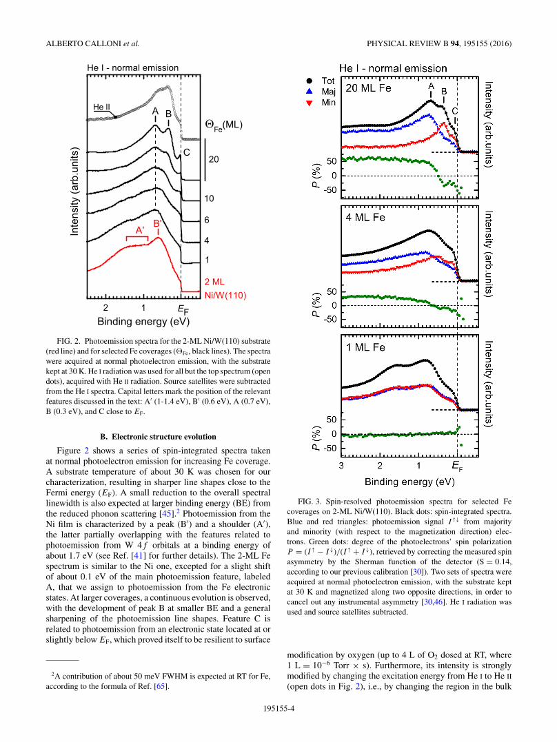
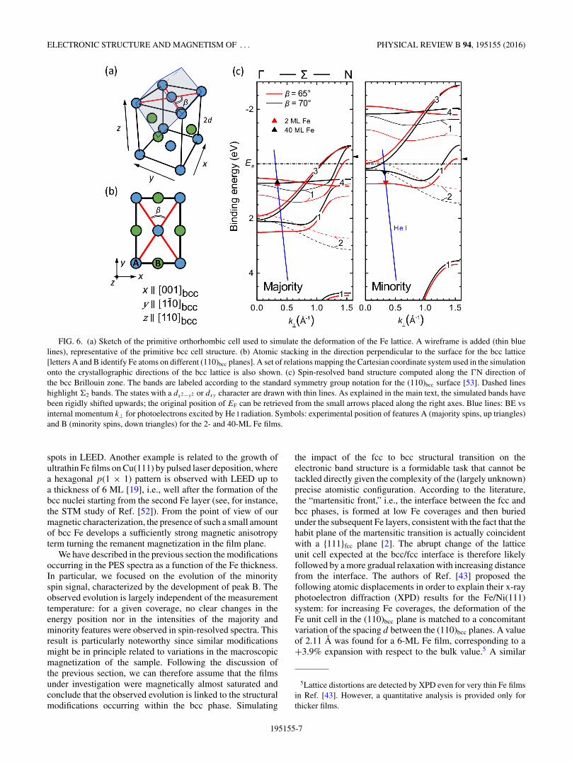
FIG. 6. (a) Sketch of the primitive orthorhombic cell used to simulate the deformation of the Fe lattice. A wireframe is added (thin bluelines), representative of the primitive bcc cell structure. (b) Atomic stacking in the direction perpendicular to the surface for the bcc lattice[letters A and B identify Fe atoms on different (110)bcc planes]. A set of relations mapping the Cartesian coordinate system used in the simulationonto the crystallographic directions of the bcc lattice is also shown. (c) Spin-resolved band structure computed along the �N direction ofthe bcc Brillouin zone. The bands are labeled according to the standard symmetry group notation for the (110)bcc surface [53]. Dashed lineshighlight �2 bands. The states with a dx2−y2 or dxy character are drawn with thin lines. As explained in the main text, the simulated bands havebeen rigidly shifted upwards; the original position of EF can be retrieved from the small arrows placed along the right axes. Blue lines: BE vsinternal momentum k⊥ for photoelectrons excited by He I radiation. Symbols: experimental position of features A (majority spins, up triangles)and B (minority spins, down triangles) for the 2- and 40-ML Fe films.
spots in LEED. Another example is related to the growth ofultrathin Fe films on Cu(111) by pulsed laser deposition, wherea hexagonal p(1 × 1) pattern is observed with LEED up toa thickness of 6 ML [19], i.e., well after the formation of thebcc nuclei starting from the second Fe layer (see, for instance,the STM study of Ref. [52]). From the point of view of ourmagnetic characterization, the presence of such a small amountof bcc Fe develops a sufficiently strong magnetic anisotropyterm turning the remanent magnetization in the film plane.
We have described in the previous section the modificationsoccurring in the PES spectra as a function of the Fe thickness.In particular, we focused on the evolution of the minorityspin signal, characterized by the development of peak B. Theobserved evolution is largely independent of the measurementtemperature: for a given coverage, no clear changes in theenergy position nor in the intensities of the majority andminority features were observed in spin-resolved spectra. Thisresult is particularly noteworthy since similar modificationsmight be in principle related to variations in the macroscopicmagnetization of the sample. Following the discussion ofthe previous section, we can therefore assume that the filmsunder investigation were magnetically almost saturated andconclude that the observed evolution is linked to the structuralmodifications occurring within the bcc phase. Simulating
the impact of the fcc to bcc structural transition on theelectronic band structure is a formidable task that cannot betackled directly given the complexity of the (largely unknown)precise atomistic configuration. According to the literature,the “martensitic front,” i.e., the interface between the fcc andbcc phases, is formed at low Fe coverages and then buriedunder the subsequent Fe layers, consistent with the fact that thehabit plane of the martensitic transition is actually coincidentwith a {111}fcc plane [2]. The abrupt change of the latticeunit cell expected at the bcc/fcc interface is therefore likelyfollowed by a more gradual relaxation with increasing distancefrom the interface. The authors of Ref. [43] proposed thefollowing atomic displacements in order to explain their x-rayphotoelectron diffraction (XPD) results for the Fe/Ni(111)system: for increasing Fe coverages, the deformation of theFe unit cell in the (110)bcc plane is matched to a concomitantvariation of the spacing d between the (110)bcc planes. A valueof 2.11 A was found for a 6-ML Fe film, corresponding to a+3.9% expansion with respect to the bulk value.5 A similar
5Lattice distortions are detected by XPD even for very thin Fe filmsin Ref. [43]. However, a quantitative analysis is provided only forthicker films.
195155-7
ALBERTO CALLONI et al. PHYSICAL REVIEW B 94, 195155 (2016)
evolution, experimentally investigated with LEED only forin-plane deformations, was observed by the authors of Ref. [2]in thin Fe films grown on 2-ML Ni/W(110). Finally, distortedbcc Fe phases (called KS-3 and KS-7 phases) have beendetected even in 2- or 3-ML Fe films on the analogous systemFe/Cu(111) [3].
We thus considered a simple model in which the electronicstructure of multilayer Fe films can be interpreted in terms ofbulk Fe bcc crystal with distorted geometry [2,43], neglectingsurface and interface effects. The pristine lattice is describedby the orthorhombic cell shown in Fig. 6(a), where the z axisis oriented along the [110] direction and the xy plane containsthe rectangular base cell corresponding to the (110)bcc surface.The deformation of the Fe lattice in the xy plane is simulatedby decreasing the β angle [Fig. 6(a)] from its value in therelaxed (110)bcc surface (70.5°) down to 65°, chosen on thebasis of the experimental results of Ref. [2]. Consideringthe nearly perfect matching between the (110)bcc and the(111)fcc diagonals [as shown in Fig. 1(d)] their length in the xy
rectangle [red lines in Figs. 6(a) and 6(b)] is kept fixed at thecharacteristic value of the relaxed bcc lattice (
√3abcc) during
the β variation. The interlayer distance d(β) was obtained bygeometry optimization. For the deformed lattice (β = 65◦),we found a value of d(65◦) which is larger (by 0.04 A) thanthe optimized spacing d(70.5◦) = 2.01 A for the relaxed cell,in nice agreement with the experimental study of Ref. [43].The band structure for β = 70.5◦ and β = 65◦ is reportedin Fig. 6(c) for the [110]bcc direction, perpendicular to thesurface (wave vector k⊥ along the � − � − N line in reciprocalspace) and probed with our system at normal electron emission(k‖ = �). The results for β = 70.5◦ are in good agreementwith the available literature on ab initio calculations on bulkFe [54–56]. Slight discrepancies do exist with the experimentalposition of the photoemission features, generally located atlower BE, which have been nevertheless well documented [57]and can be partially mended by employing more sophisticatedcomputational schemes, such as the one-step model forphotoemission, and improving the description of correlationeffects [53]. In order to facilitate the comparison between ourexperimental data and the simulations, we therefore decided toapply a rigid upward shift of 260 (180) meV for the majority(minority) states, consistent with literature results (Fig. 4(a)in Ref. [53]) related to the � point. Figure 6(c) clearly showsthat good agreement is obtained between the BE position ofthe photoemission features and the simulated band structureafter the BE scale modification. The bands have been labeledaccording to the irreducible representations of the C2v group,pertinent to the � direction [58]. Each band exhibits a smoothdependence on β, which is different according to the stateinvolved. For example, three nearly degenerate minority bandsare found around � at a BE of 0.2 eV when β = 70.5◦. Inpassing to β = 65◦, two of such states are shifted towardsEF, namely, the one labeled 3 (with dzx character) and thatlabeled 2 (with dxy character at the � point), whereas the bandlabeled 1 (with dz2 character) shifts to higher BE exhibitingthe largest variation. For the majority states observed withinabout 1 eV from EF, band 1 shifts towards larger BE, whereasband 4 is more or less stationary. The orbital character at the �
point of bands 1 and 4 is dx2−y2 and dzy , respectively. In orderto compare our experimental results with the simulated band
structure of Fig. 6(c), we estimated the photoelectrons’ internalmomentum (k⊥) following the method outlined in Ref. [59] byassuming a free-electron-like final state in a constant innerpotential V0 of 14.8 eV and a work function of 5 eV [53].The blue lines in Fig. 6(c) show the internal momentumassociated with electrons excited with He I radiation and allowto pinpoint the position of photoemission features A and B inreciprocal space for very thin (2-ML) and thick (40-ML) Fefilms. By referring to our labeling convention, feature A (B)accounts for photoemission from the majority �
↑1,4 (minority
�↓1 ) bands [53], while feature C close to EF (not shown)
is related to photoemission from the minority �↓3 band. No
emission is expected from �2 bands [dashed lines in Fig. 6(c)],which are dipole forbidden at normal emission [58], nor has itever been observed [60]. The �
↑1,4 and �
↓1 bands show almost
no energy dispersion in the �N direction, while the �↓3 band
is seen to rise steeply in energy and cross EF away fromthe � point. Feature B in the minority spectra shifts towardEF as the thickness of the Fe layer is increased; similarly,band �
↓1 moves close to its bulk position at lower BE as the
deformation of the orthorhombic Fe cell is reduced, which isconsistent with our prediction of a gradual relaxation of theFe crystal structure away from the fcc/bcc interface. FeatureA results from the superposition of the photoemission signalfrom bands �
↑1,4, which starts from different BE positions for
β = 65◦ and they merge together in bulk bcc Fe. This behaviormight explain the apparent stationary position of feature A inthe experiment, and the overall larger width of the majorityline shape with respect to the minority one (see, e.g., Fig. 3,top spectrum). In addition, we note that a lower photoemissionintensity is expected from purely in-plane orbitals dx2−y2 anddxy , if the actual values of the matrix elements for the relateddipole-allowed transitions are considered [61]. Those bandswith a prevalent dx2−y2 and dxy character are drawn withthinner lines in Fig. 6(c). By inspecting Fig. 6(c) we cantherefore conclude that the shifting band �
↑1 contributes less
than the more stationary �↑4 band to the actual position of
feature A. Finally, the �↓3 band is expected to cross EF as
the thickness of the Fe layer is increased (i.e., by increasingβ towards the bulk value), at about the same wave vectorprobed with He I radiation. We suggest that this modificationis related to the development of peak C, clearly visible inFig. 2 only for thick Fe films. The dependence upon thicknesswe observe for the dz2 orbital (feature B) is consistent with the∼2.5% increase of cell size along z when β decreases from70.5◦ to 65◦, where band narrowing is expected from simpletight binding theory.6 A seemingly simple explanation for theevolution of the dzx and dxy states is not trivially identifiable,because of the concomitant variation of the cell sizes along the
6Considering the downward curvature of the dz2 band close to �,band narrowing is expected to shift the band towards larger BE. Inorder to follow the energy dispersion of the dz2 state, one has tonotice that it hybridizes with the highly dispersing sp band, formingan avoided crossing halfway between � and N, so that band �
↓1
crossing EF at about N has a sp character while the dz2 state is foundat 4 eV BE.
195155-8
ELECTRONIC STRUCTURE AND MAGNETISM OF . . . PHYSICAL REVIEW B 94, 195155 (2016)
x(–7%) and y directions (+3.5%) and the mixed orientationof those d orbitals as well as of the nearest-neighbor atoms.The computed magnetic moment per atom is 2.17 μB, in goodagreement with other literature results for bcc Fe [62,63]and independent from the angle β in the 65◦–70.5◦ interval.Although an indirect confirmation of this result by lookingat the exchange splitting of the photoemission features isimpeded in the present case by the broad line shape of theexperimental spectra for small Fe coverages and large BE [themajority spin counterpart for feature B should be located ata BE of about 2 eV, according to Fig. 6(c)], this predictionfrom ab initio calculations is nevertheless reasonable since(i) the tetragonal deformation of the Fe cell only mildlychanges the volume per atom, which is known to directlyaffect the magnetic moment [6], and (ii) a nearly constantmagnetic moment is reported by the authors of Ref. [64] withx-ray magnetic circular dichroism (XMCD) during the fcc tobcc phase transformation for the similar Fe/Cu(111) system.
V. CONCLUSIONS
The growth of Fe on a 2-ML Ni/W(110) substrate produces,for coverages in the monolayer range, a pseudomorphic fcc
layer and no detectable in-plane magnetization. At multilayercoverage, we observe a non-nil spin polarization attributedto the onset of the fcc to bcc martensitic transition with theformation of bcc nuclei showing a KS orientation relationship.A clear restructuring of the Fe surface is visible with LEEDonly for Fe layers with a thickness larger than 4 ML. Theelectronic structure of the bcc phase is seen to continuouslyevolve with the Fe coverage towards the one expected frombulklike Fe; in particular, most of the changes observed withHe I radiation occur within the minority states. Ab initiocalculations, simulating the deformation of the bcc latticein such a way as to approximate the supposed structure ofthe metastable bcc phase, are able to reproduce the observedspectral evolution.
ACKNOWLEDGMENTS
The authors would like to thank A. Picone and F. Bot-tegoni for fruitful discussions. G.B.’s research is funded byFondazione Cariplo (Grant No. 2013-0623 SEARCH-IV).
[1] W. Martienssen and H. Warlimont, Springer Handbook ofCondensed Matter and Materials Data (Springer Science &Business Media, New York, 2006).
[2] H. L. Johnston, C. S. Arnold, and D. Venus, Thickness-dependent fcc to bcc structural change in iron films: Use ofa 2-ML Ni/W(110) substrate, Phys. Rev. B 55, 13221 (1997).
[3] A. Biedermann, W. Rupp, M. Schmid, and P. Varga, Coexistenceof fcc- and bcc-like crystal structures in ultrathin Fe films grownon Cu(111), Phys. Rev. B 73, 165418 (2006).
[4] Phase Transformations in Materials, edited by G. Kostorz(Wiley-VCH Verlag GmbH & Co. KGaA, Weinheim, FRG,2001).
[5] G. Bussetti, M. Riva, A. Picone, A. Brambilla, L. Duo, M.Finazzi, and F. Ciccacci, Martensitic transition during Ni growthon Fe(001): evidence of a precursor phase, New J. Phys. 14,053048 (2012).
[6] V. L. Moruzzi, P. M. Marcus, K. Schwarz, and P. Mohn,Ferromagnetic phases of bcc and fcc Fe, Co, and Ni, Phys.Rev. B 34, 1784 (1986).
[7] D. Bagayoko and J. Callaway, Lattice-parameter dependenceof ferromagnetism in bcc and fcc iron, Phys. Rev. B 28, 5419(1983).
[8] J. C. Boettger, Strain-dependent band-structure effects in themagnetic moment of a hexagonal Fe monolayer, Phys. Rev. B47, 1138(R) (1993).
[9] Magnetism and Structure in Systems of Reduced Dimension,edited by F. C. Farrow, B. Dieny, M. Donath, A. Fert, and B. D.Hermsmeier (Springer US, Boston, MA, 1993).
[10] F. Ciccacci and S. De Rossi, Empty electronic states in magneticthin films: Fe on Au(100), Ag(100), and Cu(100), Phys. Rev. B51, 11538 (1995).
[11] P. Allongue, F. Maroun, H. F. Jurca, N. Tournerie, G. Savidand,and R. Cortes, Magnetism of electrodeposited ultrathin layers:Challenges and opportunities, Surf. Sci. 603, 1831 (2009).
[12] M. A. Nino, J. Camarero, L. Gomez, J. Ferron, J. J. deMiguel, and R. Miranda, Surfactant-assisted epitaxial growthand magnetism of Fe films on Cu(111), J. Phys.: Condens. Matter20, 265008 (2008).
[13] S. Andrieu, M. Piecuch, and J. F. Bobo, Fe growth on (0001) hcpRu and (111) fcc Ir: Consequences for structural and magneticproperties, Phys. Rev. B 46, 4909 (1992).
[14] K. von Bergmann, S. Heinze, M. Bode, G. Bihlmayer, S. Blugel,and R. Wiesendanger, Complex magnetism of the Fe monolayeron Ir(111), New J. Phys. 9, 396 (2007).
[15] T. Allmers and M. Donath, Magnetic properties of Fe filmson flat and vicinal Au(111): Consequences of different growthbehavior, Phys. Rev. B 81, 064405 (2010).
[16] L. Hammer, S. Muller, and K. Heinz, Fe/Cu(100)—a test casefor the understanding of epitaxially grown magnetic thin films,Surf. Sci. 569, 1 (2004).
[17] H. L. Meyerheim, J.-M. Tonnerre, L. Sandratskii, H. C. N.Tolentino, M. Przybylski, Y. Gabi, F. Yildiz, X. L. Fu, E.Bontempi, S. Grenier, and J. Kirschner, New Model forMagnetism in Ultrathin fcc Fe on Cu(001), Phys. Rev. Lett.103, 267202 (2009).
[18] F. Himpsel, Exchange Splitting of Epitaxial fcc Fe/Cu(100)versus bcc Fe/Ag(100), Phys. Rev. Lett. 67, 2363 (1991).
[19] J. Shen, P. Ohresser, C. V. Mohan, M. Klaua, J. Barthel, andJ. Kirschner, Magnetic Moment of fcc Fe(111) Ultrathin Filmsby Ultrafast Deposition on Cu(111), Phys. Rev. Lett. 80, 1980(1998).
[20] A. Biedermann, R. Tscheließnig, M. Schmid, and P. Varga,Crystallographic Structure of Ultrathin Fe Films on Cu(100),Phys. Rev. Lett. 87, 086103 (2001).
[21] M. Donath, M. Pickel, A. B. Schmidt, and M. Weinelt,Ferromagnetic Fe on Cu(001) throughout the fcc-like phase:arguing from the viewpoint of the electronic structure, J. Phys.:Condens. Matter. 21, 134004 (2009).
195155-9
ALBERTO CALLONI et al. PHYSICAL REVIEW B 94, 195155 (2016)
[22] T. Burkert, O. Eriksson, S. I. Simak, A. V. Ruban, B. Sanyal, L.Nordstrom, and J. M. Wills, Magnetic anisotropy of L10 FePtand Fe1−xMn, Phys. Rev. B 71, 134411 (2005).
[23] T. Burkert, L. Nordstrom, O. Eriksson, and O. Heinonen, GiantMagnetic Anisotropy in Tetragonal FeCo Alloys, Phys. Rev.Lett. 93, 027203 (2004).
[24] A. Moser, K. Takano, D. T. Margulies, M. Albrecht, Y. Sonobe,Y. Ikeda, S. Sun, and E. E. Fullerton, Magnetic recording:advancing into the future, J. Phys. D: Appl. Phys. 35, R157(2002).
[25] C. Chappert, A. Fert, and F. N. Van Dau, The emergence of spinelectronics in data storage, Nat. Mater. 6, 813 (2007).
[26] J. Gloss, S. Shah Zaman, J. Jonner, Z. Novotny, M. Schmid,P. Varga, and M. Urbanek, Ion-beam-induced magnetic andstructural phase transformation of Ni-stabilized face-centered-cubic Fe films on Cu(100), Appl. Phys. Lett. 103, 262405(2013).
[27] A. Picone, G. Bussetti, M. Riva, A. Calloni, A. Brambilla, L.Duo, F. Ciccacci, and M. Finazzi, Oxygen-assisted Ni growth onFe(001): Observation of an “anti-surfactant” effect, Phys. Rev.B 86, 075465 (2012).
[28] E. Bauer and J. H. van der Merwe, Structure and growth ofcrystalline superlattices: From monolayer to superlattice, Phys.Rev. B 33, 3657 (1986).
[29] K.-P. Kamper, W. Schmitt, D. A. Wesner, and G. Guntherodt,Thickness dependence of the spin- and angle-resolved photoe-mission of ultrathin, epitaxial Ni(111)/W(110) layers, Appl.Phys. A: Solids Surf. 49, 573 (1989).
[30] G. Berti, A. Calloni, A. Brambilla, G. Bussetti, L. Duo, andF. Ciccacci, Direct observation of spin-resolved full and emptyelectron states in ferromagnetic surfaces, Rev. Sci. Instrum. 85,073901 (2014).
[31] C. Kozioł, G. Lilienkamp, and E. Bauer, Electronic propertiesof ultrathin nickel films on W(110), Phys. Rev. B 41, 3364(1990).
[32] K. Miyamoto, A. Kimura, K. Kuroda, T. Okuda, K. Shimada,H. Namatame, M. Taniguchi, and M. Donath, Spin-PolarizedDirac-Cone-Like Surface State with d Character at W(110),Phys. Rev. Lett. 108, 066808 (2012).
[33] R. H. Gaylord and S. D. Kevan, Spin-orbit-interaction-inducedsurface resonance on W(011), Phys. Rev. B 36, 9337(R) (1987).
[34] D. Sander, A. Enders, C. Schmidthals, J. Kirschner, H. L. John-ston, C. S. Arnold, and D. Venus, Structure and perpendicularmagnetization of Fe/Ni(111) bilayers on W(110), J. Appl. Phys.81, 4702 (1997).
[35] F. B. Dunning, Mott electron polarimetry, Nucl. Instrum.Methods Phys. Res., Sect. A 347, 152 (1994).
[36] J. P. Perdew, K. Burke, and M. Ernzerhof, Generalized Gra-dient Approximation Made Simple, Phys. Rev. Lett. 77, 3865(1996).
[37] P. Giannozzi, S. Baroni, N. Bonini, M. Calandra, R. Car, C.Cavazzoni, D. Ceresoli, G.L. Chiarotti, M. Cococcioni, I. Dabo,A. Dal Corso, S. de Gironcoli, S. Fabris, G. Fratesi, R. Gebauer,U. Gerstmann, C. Gougoussis, A. Kokalj, M. Lazzeri, L. Martin-Samos et al. QUANTUM ESPRESSO: a modular and open-sourcesoftware project for quantum simulations of materials, J. Phys.:Condens. Matter. 21, 395502 (2009).
[38] A. Picone, G. Fratesi, M. Riva, G. Bussetti, A. Calloni, A.Brambilla, M. I. Trioni, L. Duo, F. Ciccacci, and M. Finazzi,
Self-organized chromium oxide monolayers on Fe(001), Phys.Rev. B 87, 085403 (2013).
[39] A. Picone, M. Riva, G. Fratesi, A. Brambilla, G. Bussetti, M.Finazzi, L. Duo, and F. Ciccacci, Enhanced Atom Mobility onthe Surface of a Metastable Film, Phys. Rev. Lett. 113, 046102(2014).
[40] M. Riva, A. Picone, D. Giannotti, A. Brambilla, G. Fratesi,G. Bussetti, L. Duo, F. Ciccacci, and M. Finazzi, Mesoscopicorganization of cobalt thin films on clean and oxygen-saturatedFe(001) surfaces, Phys. Rev. B 92, 115434 (2015).
[41] A. Calloni, G. Bussetti, G. Berti, R. Yivlialin, A. Camera,M. Finazzi, L. Duo, and F. Ciccacci, Electronic and magneticstructure of ultra-thin Ni films grown on W(110), J. Magn. Magn.Mater. 420, 356 (2016).
[42] T. Allmers and M. Donath, Growth and morphology of thin Fefilms on flat and vicinal Au(111): a comparative study, New J.Phys. 11, 103049 (2009).
[43] G. C. Gazzadi, F. Bruno, R. Capelli, L. Pasquali, and S.Nannarone, Structural transition in Fe ultrathin epitaxial filmsgrown on Ni(111), Phys. Rev. B 65, 205417 (2002).
[44] B. An, L. Zhang, S. Fukuyama, and K. Yokogawa, Growth andstructural transition of Fe ultrathin films on Ni(111) investigatedby LEED and STM, Phys. Rev. B 79, 085406 (2009).
[45] F. Bottegoni, A. Calloni, G. Bussetti, A. Camera, C. Zucchetti,M. Finazzi, L. Duo, and F. Ciccacci, Spin polarized surfaceresonance bands in single layer Bi on Ge(111), J. Phys.:Condens. Matter. 28, 195001 (2016).
[46] G. C. Burnett, T. J. Monroe, and F. B. Dunning, High-efficiency retarding-potential Mott polarization analyzer, Rev.Sci. Instrum. 65, 1893 (1994).
[47] I.-G. Baek, H. G. Lee, H.-J. Kim, and E. Vescovo, Spinreorientation transition in Fe(110) thin films: The role of surfaceanisotropy, Phys. Rev. B 67, 075401 (2003).
[48] H. L. Meyerheim, D. Sander, R. Popescu, J. Kirschner, O.Robach, and S. Ferrer, Spin Reorientation and StructuralRelaxation of Atomic Layers: Pushing the Limits of Accuracy,Phys. Rev. Lett. 93, 156105 (2004).
[49] H. J. Elmers, J. Hauschild, H. Hoche, U. Gradmann, H. Bethge,D. Heuer, and U. Kohler, Submonolayer Magnetism of Fe(110)on W(110): Finite Width Scaling of Stripes and Percolationbetween Islands, Phys. Rev. Lett. 73, 898 (1994).
[50] G. Isella, R. Bertacco, M. Zani, L. Duo, and F. Ciccacci,Evolution of the magnetic and electronic properties of ultrathinCr(001) films, Solid State Commun. 116, 283 (2000).
[51] M. P. Seah and W. A. Dench, Quantitative electron spectroscopyof surfaces: A standard data base for electron inelastic mean freepaths in solids, Surf. Interface Anal. 1, 2 (1979).
[52] G. Rauchbauer, A. Buchsbaum, H. Schiechl, P. Varga, M.Schmid, and A. Biedermann, Ultra-thin Fe films grown on Cuby pulsed laser deposition: Intermixing and bcc-like structures,Surf. Sci. 602, 1589 (2008).
[53] J. Sanchez-Barriga, J. Fink, V. Boni, I. Di Marco, J. Braun, J.Minar, A. Varykhalov, O. Rader, V. Bellini, F. Manghi, H. Ebert,M. I. Katsnelson, A. I. Lichtenstein, O. Eriksson, W. Eberhardt,and H. A. Durr, Strength of Correlation Effects in the ElectronicStructure of Iron, Phys. Rev. Lett. 103, 267203 (2009).
[54] J. Sanchez-Barriga, J. Braun, J. Minar, I. Di Marco, A.Varykhalov, O. Rader, V. Boni, V. Bellini, F. Manghi, H. Ebert,M. I. Katsnelson, A. I. Lichtenstein, O. Eriksson, W. Eberhardt,
195155-10
ELECTRONIC STRUCTURE AND MAGNETISM OF . . . PHYSICAL REVIEW B 94, 195155 (2016)
H. A. Durr, and J. Fink, Effects of spin-dependent quasiparticlerenormalization in Fe, Co, and Ni photoemission spectra:Anexperimental and theoretical study, Phys. Rev. B 85, 205109(2012).
[55] J. Callaway and C. S. Wang, Energy bands in ferromagneticiron, Phys. Rev. B 16, 2095 (1977).
[56] J. Redinger, C. L. Fu, A. J. Freeman, U. Konig, and P. Wein-berger, Theoretical spin- and angle-resolved photoemissionspectra from Fe(110), Phys. Rev. B 38, 5203 (1988).
[57] A. M. Turner, A. W. Donoho, and J. L. Erskine, Experimentalbulk electronic properties of ferromagnetic iron, Phys. Rev. B29, 2986 (1984).
[58] W. Eberhardt and F. J. Himpsel, Dipole selection rules for opticaltransitions in the fcc and bcc lattices, Phys. Rev. B 21, 5572(1980).
[59] F. J. Himpsel, Experimental determination of bulk energy banddispersions, Appl. Opt. 19, 3964 (1980).
[60] A. M. Turner and J. L. Erskine, Exchange splitting and critical-point binding energies for iron (110), Phys. Rev. B 25, 1983(1982).
[61] X.-P. Wang, P. Richard, Y.-B. Huang, H. Miao, L. Cevey,N. Xu, Y.-J. Sun, T. Qian, Y.-M. Xu, M. Shi, J.-P. Hu, X.Dai, and H. Ding, Orbital characters determined from Fermisurface intensity patterns using angle-resolved photoemissionspectroscopy, Phys. Rev. B 85, 214518 (2012).
[62] A. Calloni, G. Berti, A. Brambilla, G. Bussetti, M. Finazzi,L. Duo, F. Ciccacci, and G. Fratesi, Magnetism in thin Crfilms grown on Fe(001)-p(1×1)O: a spin-resolved investiga-tion of single and multi-layers, Proc. SPIE 9551, 95511K(2015).
[63] P. Błonski, A. Kiejna, and J. Hafner, Theoretical study of oxygenadsorption at the Fe(110) and (100) surfaces, Surf. Sci. 590, 88(2005).
[64] P. Ohresser, G. Ghiringhelli, O. Tjernberg, N. B. Brookes,and M. Finazzi, Magnetism of nanostructures studied by x-raymagnetic circular dichroism: Fe on Cu(111), Phys. Rev. B 62,5803 (2000).
[65] T. Miller and T.-C. Chiang, Lineshape effects in photoemissionfrom the valence states of metals, J. Phys.: Condens. Matter. 13,11115 (2001).
195155-11