Embed Size (px)
Citation preview
Università degli studi di Milano Facoltà di Scienze Matematiche, Fisiche e Naturali
Laurea Triennale in Fisica
Electronic Structure of Hetero-Crystalline Superlattices
Relatore: Prof. Nicola Manini
Correlatore: Prof. Giovanni Onida
A.A. 2011/2012
Gabriele Faraone
Matricola n° 707218
Codice PACS: 73.21.-b

1
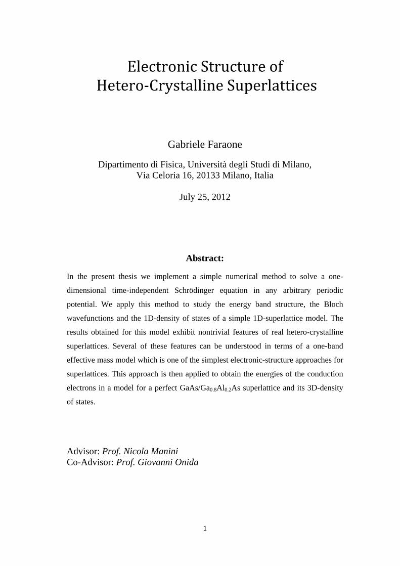
Electronic Structure of Hetero-Crystalline Superlattices
Gabriele Faraone
Dipartimento di Fisica, Università degli Studi di Milano,
Via Celoria 16, 20133 Milano, Italia
July 25, 2012
Abstract:
In the present thesis we implement a simple numerical method to solve a one-
dimensional time-independent Schrödinger equation in any arbitrary periodic
potential. We apply this method to study the energy band structure, the Bloch
wavefunctions and the 1D-density of states of a simple 1D-superlattice model. The
results obtained for this model exhibit nontrivial features of real hetero-crystalline
superlattices. Several of these features can be understood in terms of a one-band
effective mass model which is one of the simplest electronic-structure approaches for
superlattices. This approach is then applied to obtain the energies of the conduction
electrons in a model for a perfect GaAs/Ga0.8Al0.2As superlattice and its 3D-density
of states.
Advisor: Prof. Nicola Manini
Co-Advisor: Prof. Giovanni Onida

2
Contents
1 Introduction ........................................................................................................ 3
2 Superlattices Materials and Properties ............................................................... 5
2.1 Natural and Synthetic Superlattices .............................................................. 5
2.2 Semiconductor barriers and wells ................................................................ 8
3 One-Dimensional Schrödinger equation in arbitrary periodic potentials ........... 12
3.1 Method of solution ..................................................................................... 12
3.1.1 Some results on periodic differential equations .................................. 14
3.1.2 Bloch waves and energy dispersion relation ........................................ 16
3.2 Numerical implementation ......................................................................... 19
3.3 Test cases .................................................................................................... 21
3.3.1 Free particle ......................................................................................... 21
3.3.2 Kronig-Penney potential ...................................................................... 23
4 Electronic Structure of 1D-Superlattices ............................................................ 29
4.1 Energy Bands and Density of States ............................................................ 29
4.2 Superlattice Bloch wavefunctions ............................................................... 33
5 The effective mass approximation in hetero-crystalline superlattices ............... 39
5.1 Brief summary on superlattice electronic structure methods.................... 39
5.2 One-Band effective mass model ................................................................. 41
5.3 Result on superlattice minibands and 3D-Density of States ....................... 45
6 Discussion and Conclusions ............................................................................... 50
References ............................................................................................................... 52
3
1 Introduction
Mesoscopic systems
One of the most striking trends of the modern microelectronic and semiconductor
industry is the miniaturization of the electronic devices.
Due to the development of sophisticated growth techniques it is possible nowadays
to fabricate nanometer scale semiconductor structures (often abbreviated as
nanostructures). The linear sizes of these artificially structured materials in one, two,
or even three spatial dimensions are of the order of the de-Broglie wavelength of the
current-carrying electrons. For electrons confined to such small regions quantum
effects and the quantized nature of the energy spectrum become important for an
accurate description of the electronic and thermodynamic properties. Depending on
the direction in which the free propagation of electrons is confined these structures
are called: quantum wells (QWs) if they display one-dimensional quantum
confinement, quantum wires if electrons are confined in two directions or quantum
dots if electrons are confined in all three directions.
In this thesis we will focus on the study of the electronic structure of layered
nanostructures, such as Multiple Quantum Wells (MQWs) or Superlattices (SLs),
realized by growing alternate layers of two dissimilar materials on top of each other.
In these structures the periodic modulation of the materials affects only the
electronic-motion along the growth axis and it can be ideally modeled as the motion
of particles in a one-dimensional infinite-periodic potential. Under appropriate
circumstances this one-dimensional “artificial periodicity” perturbs the energy bands
of the host materials, yielding a series of narrow subbands and forbidden gaps along
the growth direction.
Superlattices and MQWs are similar in construction except that the inter-well-
separation in MQWs is large enough to prevent electrons from tunneling from one
well to the next. These structures have peculiar electronic properties (e.g. negative
differential resistance, Bloch oscillations, etc.) which make them suitable for a broad
range of uses ranging from telecommunications to optoelectronics.

4
Since the linear sizes of the confinement region in these systems are smaller than one
micron, typically a few hundred nanometers, they are also referred to as
“mesoscopic”. Mesoscopic means that the involved length scales are halfway
between the typical length scales of bulk materials ( ) and atomic (
) samples. In these situations electron wavefunctions maintain a phase
coherence during the transport across the entire structure, i.e., the relevant system
size is usually smaller than the electron “phase coherence length” and, roughly, the
electron mean free path. Thus, a condition to observe quantum effects in a
Superlattice and in similar layered structures is that the mean free path of the
electrons must be significantly larger than the period of the potential modulation, in
order to preserve phase coherence. Under these conditions SLs become elegant
examples of 1D-physics problems which constitute, to all intent and purposes,
meaningful models of reality.
In this thesis our main goal will be to obtain some properties of the electronic
structure of superlattices calculating them in a simplified but realistic one-
dimensional model. In section 2 we review the basic properties of SLs from the point
of view of materials used in the fabrication of layered semiconductor structures.
Section 3 reports the method used to solve a one-dimensional time-independent
Schrödinger equation in any arbitrary periodic potential and the numerical
implementation on simple test cases.
Our code is then applied in section 4 to calculate the energy bands, the density of
states and the wavefunctions for a one-dimensional superlattice model. The results
obtained in this case give a meaningful insight into the electronic properties of real
superlattices and allow us to introduce, in section 5, the effective mass
approximation which is one of the simplest approach for SL electronic structure
calculations. We discuss this approximation under simplified assumptions,
specifically, in a one-band model and subsequently we apply it to obtain the energy
levels of the conduction electrons in a ideally infinite GaAs/Ga1-xAlxAs superlattice
and the 3D-Density of States. Finally, section 6 holds the final discussion and
conclusion.
5
2 Superlattices Materials and Properties
2.1 Natural and Synthetic Superlattices
Superlattice structures exist in nature either in the form of metal alloys or polytype
semiconductors.
Some crystals, such as hexagonal SiC, have a number of different structural forms
known as polytypes in which is possible the formation of a natural one-dimensional
superlattice structure with a period ranging from 1.5 to 5.3 nm [1]. However these
polytype structures cannot be controlled and the resulting energy gaps are too small
to provide any useful electronic application.
Long-period crystal structures have also been found in natural face-centered cubic
metal alloys having compositions around AB and A3B. The superlattice CuAu-II in
the Cu-Au alloy system is a classic example of this type of structure [2]. The
superlattice consists of antiphase boundaries with no change in the underlying lattice
across them, but with two types of atoms differently ordered. These antiphase
structures are characterized by a super-period that exists only in one direction;
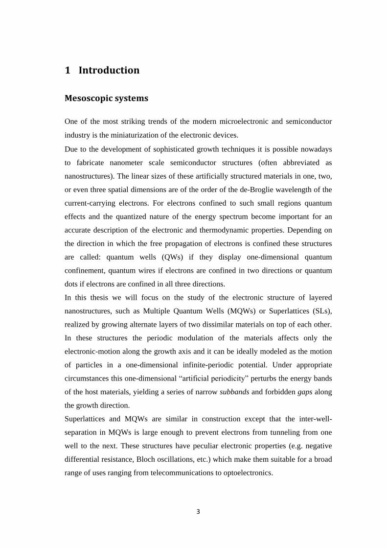
therefore we can describe them by using a long unit cell composed of a row of
fundamental unit cells of the face-centered cubic lattice, in the direction of the
period, as shown in Fig. 2.1
Synthetic artificial superlattices were proposed theoretically for the first time in 1970
by Esaki and Tsu [3] who investigated the properties of one-dimensional periodic
potentials and negative differential conductivity in semiconductors. They envisioned
two kinds of “artificial” superlattices: compositional and doping.
Fig.2.1: One unit cell of the orthorhombic superlattice of CuAu. The copper and gold atoms form
alternate layers, but their relative positions change at regular intervals (antiphase boundaries) so
that the unit cell consists of 10 of the simple face-centred cubic cells.
6
In compositional superlattices the modulation of the electronic potential along the
growth direction is achieved by periodic variation of alloy composition, introduced
during the crystal growth. The thickness of the alternating layers is between a few
Angstroms and a few hundred Angstroms. Doping superlattices consists of
alternating n- and p-type layers of a single semiconductor. In these superlattices the
electric fields generated by the charged dopants modulate the electronic potential.
In compositional superlattices the pair of materials chosen to form the alternate
layers should have lattice constants that match closely so that the interface from one
material to the other carries as little strain as possible. This kind of lattice alignment
is known as pseudomorphic growth and is highly desirable for achieving high-quality
hetero-crystalline structures.
The method of growing thin crystalline layers from a crystalline substrate of different
material is known as heteroepitaxy. Heteroepitaxy is of primary importance as a
means of fabricating semiconductor superlattices. Innovations and improvements in
growth techniques such as MBE (molecular beam epitaxy), MOCVD (metallo
organic chemical vapor deposition) and MOMBE (metallo organic molecular beam
epitaxy) during the last decade have made possible high-quality heterostructures.
Such structures possess predesigned potential profiles and impurity distributions with
dimensional control close to interatomic spacing and with virtually defect-free
interfaces.
Semiconductor materials used to fabricate the superlattice structures are the III-V, II-
VI and IV-VI compounds, as well as elemental semiconductors. Among the III-V
semiconductors the GaAs/Ga1-xAlxAs heterostructures have been extensively studied.
In particular GaAs/AlAs system are the most favored to realize lattice matched
structures due to the small difference between the GaAs and AlAs lattice constants:
only 0.15% lattice mismatch. The first compositional superlattice was realized with a
GaAs/Ga1-xAlxAs material system [4].
Figure 2.2 shows the relationship between the lattice constant and the low-
temperature energy band-gap for typical semiconductors with the diamond and zinc-
blende structures. The shaded regions show the groups of semiconductors with
similar lattice constants that can be combined to form lattice matched systems.

7
It is also possible to grow lattice-mismatched superlattices with essentially no
dislocation defects generation at the interfaces if the layers are sufficiently thin. In
this situation the lattice-constant mismatch is accommodated by coherent strain in the
individual layers. This kind of superlattices are called Strained-Layer Superlattices
(SLS). One example is the SixGe1-x system where the lattice mismatch is about 4%.
In such structures, however, there exists a critical layer thickness beyond which the
crystalline structure releases its strain creating misfit dislocations.
The modern growth techniques also allow to control the artificial periodicity of the
superlattices structures in various ways. The simplest complexity that can be added
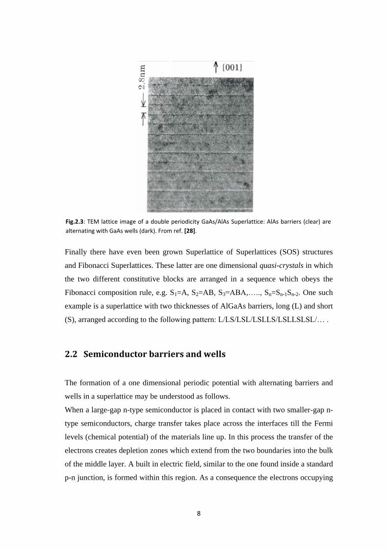
to a mono-periodic array is a double-periodicity. Figure 2.3 show a cross-sectional
image taken by high-resolution Transmission Electron Microscopy (TEM) of a
double period GaAs/AlAs superlattice where AlAs layers of alternating 0.45 nm and
0.90 nm thickness are interposed in between GaAs layers of equal 3.2 nm thickness.
Fig.2.2: Lattice constant versus low temperature band-gaps for semiconductors with the diamond
and zinc-blende structure. Semiconductors joined by solid lines can form stable alloys. Broken lines
indicate indirect band-gap alloys. The negative band-gap that can be seen for HgSe and HgTe is still
controversial. Adapted from ref. [7].
8
Finally there have even been grown Superlattice of Superlattices (SOS) structures
and Fibonacci Superlattices. These latter are one dimensional quasi-crystals in which
the two different constitutive blocks are arranged in a sequence which obeys the
Fibonacci composition rule, e.g. S1=A, S2=AB, S3=ABA,….., Sn=Sn-1Sn-2. One such
example is a superlattice with two thicknesses of AlGaAs barriers, long (L) and short
(S), arranged according to the following pattern: L/LS/LSL/LSLLS/LSLLSLSL/… .
2.2 Semiconductor barriers and wells
The formation of a one dimensional periodic potential with alternating barriers and
wells in a superlattice may be understood as follows.
When a large-gap n-type semiconductor is placed in contact with two smaller-gap n-
type semiconductors, charge transfer takes place across the interfaces till the Fermi
levels (chemical potential) of the materials line up. In this process the transfer of the
electrons creates depletion zones which extend from the two boundaries into the bulk
of the middle layer. A built in electric field, similar to the one found inside a standard
p-n junction, is formed within this region. As a consequence the electrons occupying
Fig.2.3: TEM lattice image of a double periodicity GaAs/AlAs Superlattice: AlAs barriers (clear) are
alternating with GaAs wells (dark). From ref. [28].
9
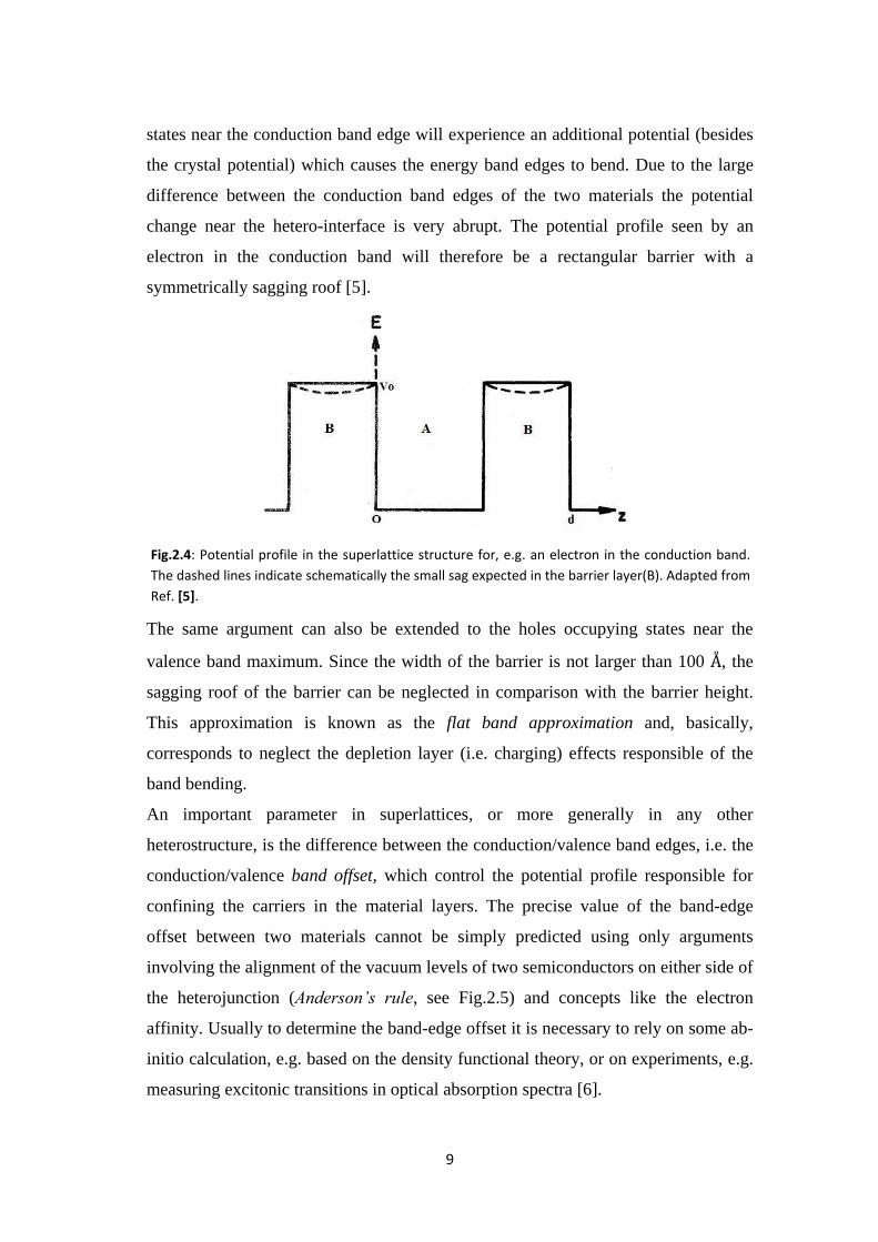
states near the conduction band edge will experience an additional potential (besides
the crystal potential) which causes the energy band edges to bend. Due to the large
difference between the conduction band edges of the two materials the potential
change near the hetero-interface is very abrupt. The potential profile seen by an
electron in the conduction band will therefore be a rectangular barrier with a
symmetrically sagging roof [5].
The same argument can also be extended to the holes occupying states near the
valence band maximum. Since the width of the barrier is not larger than 100 , the
sagging roof of the barrier can be neglected in comparison with the barrier height.
This approximation is known as the flat band approximation and, basically,
corresponds to neglect the depletion layer (i.e. charging) effects responsible of the
band bending.
An important parameter in superlattices, or more generally in any other
heterostructure, is the difference between the conduction/valence band edges, i.e. the
conduction/valence band offset, which control the potential profile responsible for
confining the carriers in the material layers. The precise value of the band-edge
offset between two materials cannot be simply predicted using only arguments
involving the alignment of the vacuum levels of two semiconductors on either side of
the heterojunction (Anderson’s rule, see Fig.2.5) and concepts like the electron
affinity. Usually to determine the band-edge offset it is necessary to rely on some ab-
initio calculation, e.g. based on the density functional theory, or on experiments, e.g.
measuring excitonic transitions in optical absorption spectra [6].
Fig.2.4: Potential profile in the superlattice structure for, e.g. an electron in the conduction band.
The dashed lines indicate schematically the small sag expected in the barrier layer(B). Adapted from
Ref. [5].

10
However, advanced epitaxial techniques have made possible the growth of extremely
abrupt interfaces, i.e as narrow as one atomic monolayer ( ). In these situations
extensive comparison between experimental results and theoretical calculation have
shown that one can retain the notion of mathematically abrupt interfaces making
Anderson’s rule a fair approximation in predicting the values of square-well
confinement potentials in most heterostructures.
Therefore, given two semiconductors A and B (with
), in the abrupt
interfaces model and the flat band approximation, is possible to make a clear
distinction between barrier acting (B) and well-acting (A) materials. Since in these
hypothesis the modeling of the confining potential in terms of an array of wells and
barriers can be considered correct, it is customary to classify SLs (or more generally
MQWs structures) according to the confinement energy schemes of their electrons
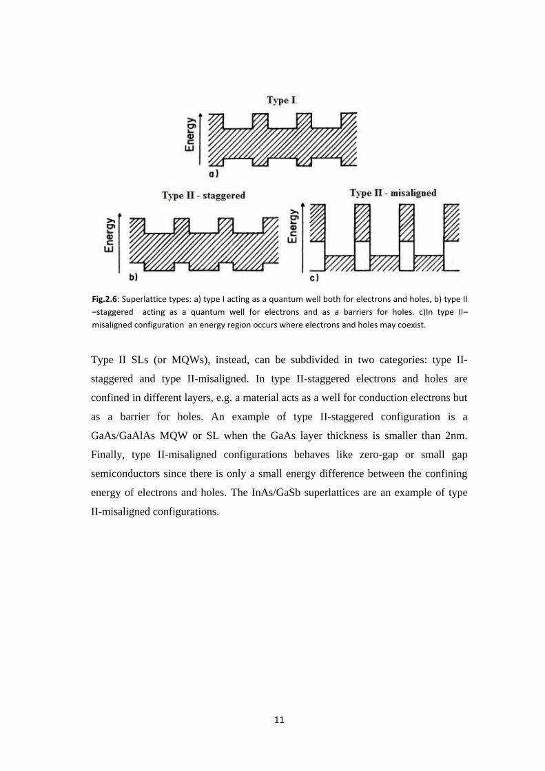
and holes. These confinement schemes are usually labeled type I and type II.
In type I SLs the electrons and holes are both confined within the same layer forming
the well (note that the notion of wells and barriers is interchanged for electrons and
holes because they have opposite energies). Examples of type I configurations are
GaAs/GaAlAs systems provided that the GaAs layer is larger than 2 nm [7].
Fig.2.5: The Anderson’s rule for predicting band offsets in a heterojunction formed by two materials
A and B (
). , are the electron affinities, , are the conduction and valence
band offsets, respectively. In Anderson's idealized model these material parameters are unchanged
when the materials are brought together to form a hetero-interface. According to Anderson’s rule:
and
. From Ref. [29].
11
Type II SLs (or MQWs), instead, can be subdivided in two categories: type II-
staggered and type II-misaligned. In type II-staggered electrons and holes are
confined in different layers, e.g. a material acts as a well for conduction electrons but
as a barrier for holes. An example of type II-staggered configuration is a
GaAs/GaAlAs MQW or SL when the GaAs layer thickness is smaller than 2nm.
Finally, type II-misaligned configurations behaves like zero-gap or small gap
semiconductors since there is only a small energy difference between the confining
energy of electrons and holes. The InAs/GaSb superlattices are an example of type
II-misaligned configurations.
Fig.2.6: Superlattice types: a) type I acting as a quantum well both for electrons and holes, b) type II
–staggered acting as a quantum well for electrons and as a barriers for holes. c)In type II–
misaligned configuration an energy region occurs where electrons and holes may coexist.

12
3 One-Dimensional Schrödinger equation in arbitrary
periodic potentials
A common feature of superlattices structures (both natural and synthetic) is the
existence of a one-dimensional “mesoscopic” periodicity superimposed to the three
dimensional “microscopic” periodicity of the crystalline lattices. To understand to
what extend the former can influence the electronic properties (such as the energy
band structure and the density of states) of the constituent materials we shall
consider, in the next chapter, a simplified one-dimensional model.
Since in this model the study of the superlattice electronic structure involve the
solution of a one dimensional Schrodinger equation in a generic periodic potential
we shall describe first how to face this problem from the computational point of
view.
3.1 Method of solution
As a starting point we consider an one dimensional time-independent Schrödinger
equation of the form:
(3.1)
where is a generic periodic potential having a periodicity d:
(3.2)
According to Bloch’s theorem [8] a complete set of solutions of Eq. (3.1) exists in
the form:
(3.3)
or equivalently in the form:
(3.4)
and the corresponding eigenvalues will be denoted by .
In (3.3) is a function of x having the same periodicity of the potential and the
n-index distinguishes between states having the same wave-number q but belonging
13
to different energy bands, . The wave-numbers q can be determined by
imposing periodic boundary conditions on considering a large (macroscopic)
number of unit cells of the infinite 1D lattice: .
Usually, all inequivalent discrete q-values are chosen to lie within the first Brillouin
zone, namely:
In the limit of very large the difference between two successive discrete q-values
within the Brillouin zone becomes infinitely small and they can be considered as a
continuum.
Our problem now is to find a numerical method for the solution of both the energy
dispersion relation and the Bloch eigenfunctions of the time-
independent Schrödinger equation (3.1) for a given periodic potential. Given it
is also useful to determine the number of available electronic states per unit energy
and per unit length, i.e. the one-dimensional Density of States (1D-DoS). This is
given by the following expression:
(3.5)
where the factor 2 accounts for the two-fold spin degeneracy and the degeneracy of
and Bloch states having the same energy.
A possible approach to solve Eq. (3.1) is to consider the equation for the periodic
part of the Bloch wavefunctions obtained by substituting the (3.3) in (3.1):
(3.6)
This equation can be solved in a single unit cell of the lattice, say in the interval
, imposing periodic boundary conditions on and its derivative:
(3.7)
However, this kind of approach has an implicit difficulty precisely due to the latter
requirement. On the one hand, to integrate Eq. (3.6), we need to fix a precise value
for both and its derivative at the boundaries of the unit cell. On the other
hand the boundary conditions in (3.7) does not indicate how we have to choose these
two values. In fact, although one of them is arbitrary, since wavefunctions are
14
computed up to a normalization factor, the ratio
remains however undefined
and it would be necessary to determine it by solving a complicated 2-dimensional
inverse problem. Another difficulty of this approach is that we have to face the
integration of a second-order differential equation with complex coefficients and
having also a complex-valued solution, .
However, we can address the solution of Eq. (3.1) in an independent fashion. An
useful suggestion comes from the fact that, as stated above, the Bloch functions
and are degenerate (same energy). This is the main idea behind the simple
numerical method adopted in the present thesis which we shall explain in the
following sections. In sect. 3.1.1 we shall give a brief review on some mathematical
aspects concerning the Floquet’s theory of periodic differential equations. This
theory will come in handy in 3.1.2 to explain the method designed for solving Eq.
(3.1). In sect. 3.2 we briefly describe the numerical implementation of the method
and, finally, in sect. 3.3 we test it in two simple cases: free particle and a Kronig-
Penney potential.
3.1.1 Some results on periodic differential equations
Mathematically Eq. (3.1) with the periodic potential (3.2) is a homogeneous linear
differential equation of second order with real and periodic coefficients. Any
equation of this kind can be reduced to an equation of Hill’s type [9] of the form:
(3.8)
Where is a real-valued, piecewise continuous and periodic function with a
minimal period p: and is a parameter.
This problem has many features in common with the periodic Sturm-Liouville
problems, and in certain cases it can be reduced to ordinary boundary-value problems
of the Sturm-Liouville type.
We are typically interested in determining the set of all for which the solutions
of (3.8) are stable, i.e., bounded: this is known as direct periodic spectral problem
and the set of all thus obtained is known as the spectrum (i.e the eigenvalues)
of the self-adjoint linear operator
on lhs of Eq. (3.8). It can be shown
15
(Ref. [9] pg. 11) that the spectrum of (3.8) is bounded from below and consists of the
union of a infinite sequence of intervals (stability intervals):
with:
(3.9)
such that the length of the separating gaps between intervals tends to zero as .
Moreover, let and be two linearly independent solutions of (3.8)
defined by a given value for and by the following choice for the initial conditions:
(3.10)
These solutions are referred to as normalized solutions of (3.8).
It can be proved that and are stable in the previous intervals and the
numbers are the roots of the equation while the numbers are those of
where:
(3.11)
is called the discriminant of Hill’s equation.
Since and form a basis for the space of solutions, for a given , it is
possible to construct two linearly independent solutions of (3.8) as linear
combinations of and :
(3.12)
If lies in a stability interval it can be proven that and are real and
the two linearly independent solutions of the type (3.12) can be written in “Bloch’s
form” :
(3.13)
where and are periodic with period p and is real.
This results is a consequence of a very general theorem known as Floquet’s Theorem
(Ref. [9] pg. 4). Defining the characteristic equation associated with (3.8) as:
(3.14)
Floquet’s theorem states that if the equation (3.14) has two different roots, and
, then there exist two linearly independent solutions, and , in
Bloch form such that:
(3.15)
16
and:
(3.16)
If, instead, , then equation (3.8) has a non trivial solution which is
periodic with period p (when or equivalently when ) or
2p (when or equivalently when ).
Note that if we limit the search of the solution of (3.8) only to the periodic ones, i.e.
, which satisfy the periodic boundary conditions and
, the problem reduces to a standard periodic Sturm-Liouville problem.
However, with this choice only a subset of the spectrum in Eq. (3.9) can be obtained,
namely the unbounded sequence of eigenvalues:
An important consequence of Floquet’s theorem is the stability criterion: stable
solutions (i.e. bounded) are obtained if and only if is real and or
and . Thus, we have a condition for to be in the
spectrum, namely:
(3.17)
The relative values of are real and can be determined from the equation:
(3.18)
as immediately follows from Eqs. (3.14) and (3.16).
This equation and the condition (3.17) suggest a simple method for the determination
of the dispersion relation (more precisely, the inverse dependency ):
choose a value and compute and integrating (3.8) as an initial
value problem (IVP) with the initial conditions (3.10); then, if condition (3.17) is not
satisfied lies in a forbidden gap; if, instead, (3.17) is true then evaluate by
solving Eq. (3.18).
3.1.2 Bloch waves and energy dispersion relation
Let us apply the previous results to the solution of the simple 1-D Schrödinger
periodic problem in (3.1). We note first that a naive numerical integration of the
Schrödinger equation (3.1) with fixed initial conditions for and does not
automatically give a solution of the Bloch form. As we have seen in sect. 3.1.1, the
17
second order Schrödinger equation has two linearly independent solutions for a given
. Only appropriate linear combinations of these will satisfy the Bloch condition
(3.4).
Consider two generic solutions and obtained by numerical integration
of (3.1) with a given energy value and using the following initial conditions
(derived from those of Eq. (3.10)):
(3.19)
It can be shown that two solutions of (3.1) are linearly independent if the Wronskian
is not-zero at some point x. The Wronskian of and is:
(3.20)
Since and are two solutions with the same energy it easy to show that
the Wronskian is constant and independent of x. Thus,
for any x and this proves that and are linearly independent. According
to the results of the previous section if lies in an allowed band, then and
are real and can be used to form two linearly independent solutions in the
Bloch’s form:
(3.21)
Conversely, , (and their derivatives) can be expressed as linear
combination of the two Bloch’s function with the same energy [10]:
(3.22)
The coefficients can be simply determined by solving Eq. (3.22) and can be
expressed by the Wronskians:
(3.23)
Using the initial conditions (3.19) we obtain:
18
(3.24)
To compute the wave number for a given energy value we need to evaluate
and in x=d. Substituting (3.24) in (3.22) and using the Bloch’s
condition (3.4), both for and for its derivative , we have:
(3.25)
and:
(3.26)
Thus, the Bloch momentum can be determined numerically by solving:
(3.27)
which is similar to Eq. (3.18) in the previous section.
To compute the Bloch functions in (3.21) we use (3.22) to express as linear
combinations of the numerical solutions , :
(3.28)
Since , and are solutions of the Schrödinger equation (3.1) with the same
energy, the Wronskian coefficients in (3.28) are independent of x and can be
evaluated at either boundary of the unit cell:
(3.29)
19
Substituting (3.29) in (3.28) we see that the Bloch wavefunctions, for a given energy
value, , in an allowed band, are determined by the two numerical solutions, up to a
multiplicative constant, :
(3.30)
The values of can be fixed by imposing the normalization:
3.2 Numerical implementation
Equation (3.1) is a second order differential equation but it can be recasted also into a
system of two first-order coupled differential equations:
(3.31)
with .
Having (3.1) in this form it is possible to implement a standard numerical iterative
routine for the solution of first-order differential equations with given initial
conditions. In particular, we have implemented a 5th
order Runge-Kutta method with
adaptive stepsize control [11].
The energy dispersion relation, , can be computed on a discrete energy mesh
by computing and for each energy value. At each step we check if the
absolute value of the rhs of Eq. (3.27) is greater or less than unity. In the first case
lies in a gap in the second case lies in an allowed band and we obtain the
wave number solving Eq. (3.27). This relation, moreover, automatically gives
within one half of the Brillouin zone, i.e.
. The energy band
structure in the whole Brillouin zone can be recovered extending by symmetry the
calculated values on the other half of the zone. The energy mesh step used to scan the
dispersion relation depends on the selected accuracy and on the slope of the
investigated bands. This fact constitutes a drawback for our method. In fact, since the
energy bands become stationary at the boundaries of the Brillouin zone, the band
20
profiles in these zones are never computed with sufficient accuracy. To avoid this we
have been always forced to compute using a large number of energy mesh
steps at the expenses, however, of the computing-speed.
The routine implemented for the calculation of the energy band structure, allows also
the determination of the 1D-DoS. We compute numerically the derivative
in (3.5) on the same discrete energy steps previously defined. If lies in a forbidden
gap the 1D-DoS is set zero; when, instead, the energy lies within an allowed band
Eq. (3.5) is employed to evaluate the 1D-DoS.
The Bloch wavefunctions are computed only for given input energy values. In
practice, we first check if the chosen energy value lies in an allowed band repeating
the same procedure previously described. If it is true we determine the corresponding
wave number, , and we proceed to the calculation of the real and imaginary part
of the Bloch function. For positive wave numbers, , from equation (3.30) we
obtain:
(3.32)
So, to determine and we have to know the two real
solutions and at the same points in the unit cell. For this purpose,
however, we do not integrate Eq. (3.1) directly through the unit cell, i.e. from 0 to d,
but we divide the unit cell over a mesh of small intervals and perform the numerical
integration in each of these only. In this way, storing the computed values of
and at the end of each small interval, we obtain the values of and
at the same points. This procedure, moreover, makes better use of the adaptive nature
of the Runge-Kutta algorithm in the case of rapidly varying potentials.
Once determined and , we apply the Bloch condition
(3.4) to extend the computed functions to the successive unit cells (typically on 4-5
periods) and, finally, we obtain the square-module of the Bloch function by:
(3.33)
which gives the probability distribution of the electron.
All these calculations have been implemented in a specific c++ program (gcc 3.4.4).
21
3.3 Test cases
We have tested the method developed for the solution of Eq. (3.1) on two simple
cases: null periodic potential (free-particle case), and the Kronig-Penney potential.
In both cases Eq. (3.1) is exactly solvable and the results of our numerical
calculations can be compared with the exact trends for the energy band structure,
density of states, real, imaginary and periodic part of the Bloch functions.
All calculations have been performed in Angstroms length units ( ) and electron-
volts (eV) energy units. To plot the results we used an object-oriented data-analysis
suite of programs (Root, 5.12).
3.3.1 Free particle
Putting =0 the (3.1) becomes the free particle equation in 1D. The solutions
are plane waves of the form:
(3.34)
and the energy dispersion relation is:
(3.35)
where
.
The 1D-DoS can be immediately derived from (3.5) and (3.35):
(3.36)
The real and imaginary part of the free particle wavefunction (3.34) are respectively
a cosine and a sine function with a period equal to
. The periodic part of the Bloch
wavefunction is trivial. We expect to find:
The results of our calculations are shown in Fig. 3.1 and Fig. 3.2 and follows the
expected trends.

22
Fig.3.1: Imaginary part (dotted), real part (dashed) and periodic part (solid line) of the free particle
(mass=electron mass) Bloch wavefunction having an energy of 4.176 eV and a wave number of
q=1.04693 ( ). The wavefunctions have been computed on a unit cell of the lattice (with
on a fixed x-mesh of 1000 points and successively extended on the consecutive 4 periods,
as explained in sect. 3.2.
Fig.3.2: Energy band structure and 1D-DoS of a free particle (with mass=electron mass) in a 1D-
lattice with periodicity d=3 . The values have been computed in a 25 eV range on a mesh of 3000
points. The small singularities on the 1D-DoS curve at the energies corresponding to the turning
points are consequences of the lack of a precise calculation of the band-edge points ( ,
)
in the energy dispersion relation.
23
3.3.2 Kronig-Penney potential
The periodic potential considered in this case is formed by an infinite sequence of
finite quantum wells of width , separated by barriers of width and
energy . We put the origin of the x-axis at the left-hand boundary of the well; thus
the potential in the nth-unit cell is given by:
(3.37)
The solutions of Eq. (3.1) are exactly known both in the wells and in the barriers. For
energies we have:
(3.38)
where:
(3.39)
The coefficients A, B, C, D can be determined by matching and its derivative at
and and using the Bloch’s condition (3.4) to express
and at in terms of and at . Proceeding
on this way, a 4 x 4 homogeneous system in A, B, C, D can be obtained. Non trivial
solutions exist only if the determinant of the matrix of coefficients is zero.
Expanding this determinant we end up with the following equation:
(3.40)
which implicitly determines the energy dispersion relation, . For energies
a similar equation can be obtained by taking into account that becomes
imaginary:
(3.41)
and using the following identities: ,
.
24
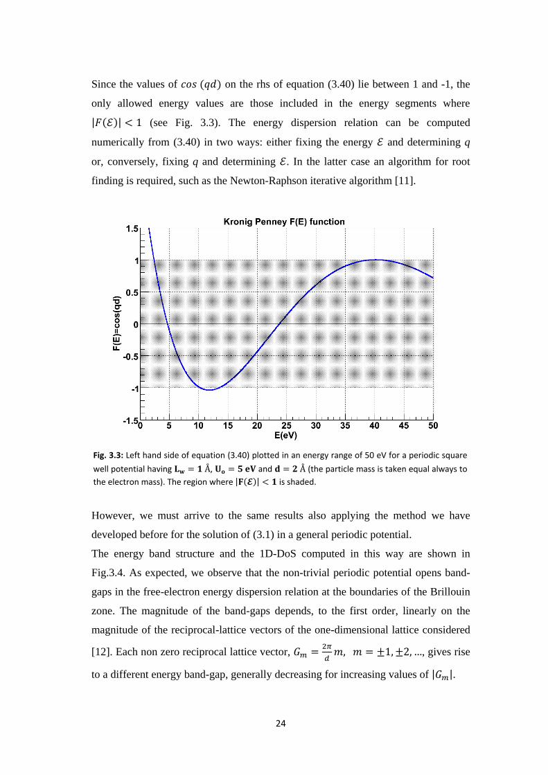
Since the values of on the rhs of equation (3.40) lie between 1 and -1, the
only allowed energy values are those included in the energy segments where
(see Fig. 3.3). The energy dispersion relation can be computed
numerically from (3.40) in two ways: either fixing the energy and determining q
or, conversely, fixing q and determining . In the latter case an algorithm for root
finding is required, such as the Newton-Raphson iterative algorithm [11].
However, we must arrive to the same results also applying the method we have
developed before for the solution of (3.1) in a general periodic potential.
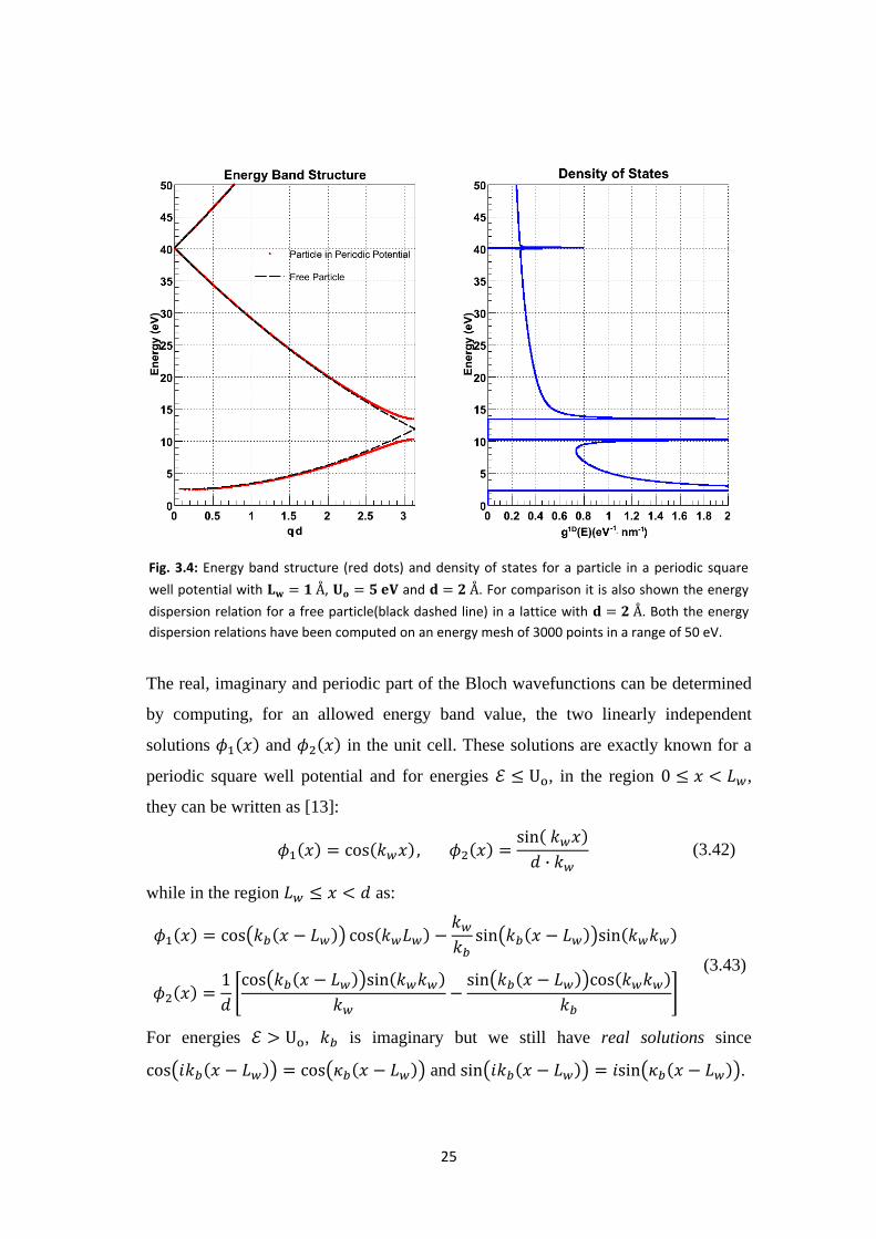
The energy band structure and the 1D-DoS computed in this way are shown in
Fig.3.4. As expected, we observe that the non-trivial periodic potential opens band-
gaps in the free-electron energy dispersion relation at the boundaries of the Brillouin
zone. The magnitude of the band-gaps depends, to the first order, linearly on the
magnitude of the reciprocal-lattice vectors of the one-dimensional lattice considered
[12]. Each non zero reciprocal lattice vector,
, gives rise
to a different energy band-gap, generally decreasing for increasing values of .
Fig. 3.3: Left hand side of equation (3.40) plotted in an energy range of 50 eV for a periodic square
well potential having , and (the particle mass is taken equal always to
the electron mass). The region where is shaded.
25
The real, imaginary and periodic part of the Bloch wavefunctions can be determined
by computing, for an allowed energy band value, the two linearly independent
solutions and in the unit cell. These solutions are exactly known for a
periodic square well potential and for energies , in the region ,
they can be written as [13]:
(3.42)
while in the region as:
(3.43)
For energies , is imaginary but we still have real solutions since
and .
Fig. 3.4: Energy band structure (red dots) and density of states for a particle in a periodic square
well potential with , and . For comparison it is also shown the energy
dispersion relation for a free particle(black dashed line) in a lattice with . Both the energy
dispersion relations have been computed on an energy mesh of 3000 points in a range of 50 eV.

26
Note, incidentally, that evaluating and in x=d and using equation (3.27)
we recover again Eq. (3.40).
The exact solutions (3.42) and (3.43) can be compared with the numerical solutions
and obtained by integrating Eq. (3.1) with initial conditions (3.19)
using an adaptive Runge- Kutta algorithm. This comparison is shown in Fig. 3.5 on a
unit cell . We report the wavefunctions computed for an energy of with
the following potential parameters: , .
As can be noticed the exact and numerical and wavefunctions agree
perfectly on the whole unit cell. This fact proves that our method for solving the
Schrödinger equation with generic periodic potentials returns good results, at least in
this exactly solvable case. Another indirect test on the accuracy of our numerical
results is provided by the comparison of the wave number values of the exact and
numerical wavefunctions and that are expressed as linear combinations
of the Bloch functions as in (3.22).
Fig. 3.5: Exact solutions (solid lines) (3.42) and (3.43) for (light blue) and (violet)
compared with numerical solution (dashed) for (dark blue) and (red). The square-well
potential (black line) is also shown.

27
The wave number of the exact solutions can be obtained directly by solving equation
(3.40) for a given energy. In the case considered, i.e. for , we have
The wave number of the numerical solutions for a given energy can
be obtained as explained in sect. 3.1.2 from Eq. (3.27). For
which is identical to the previous “exact” value in the first four
significant digits.
The small discrepancy in the latest digits may be explained by the nature of the
potential employed to perform the numerical integration. In practice, we could not
use an exact square well potential because the 5th
-order Runge Kutta numerical
integration fails at and discontinuities. Instead, we have modeled the
discontinuous steps using a smoothing function. The smoothing function modeling
the step has the following form:
(3.44)
where are unit step functions that “cut” the sine function over a semi-
period, 2b in the interval . The step can be similarly modeled
properly translating the previous expression.
Fig. 3.6: Potential rounding trend near the discontinuity at on the left-side of the square-
well potential used in the numerical calculations( , , ). The smoothing
range is .

28
matches the constant values of the potential at with vanishing
derivative and setting very small values for the parameter in (3.44) a very steep
wall can be modeled. In our calculations we have always fixed .
Finally the real, imaginary and periodic part of the Bloch wavefunction calculated
using the and numerical solutions with the previous values for the
energy and the wave number ( , are
shown in Fig. 3.7.
Fig. 3.7: Imaginary part (blue dotted), real part (violet dashed) and periodic part (red solid line) of
the Bloch wavefunction having an energy of 3 eV in a square well periodic potential (black solid
line) with , and . The values have been computed on a unit cell
and extended, as explained in sect. 3.2, on the successive 4 periods.

29
4 Electronic Structure of 1D-Superlattices
4.1 Energy Bands and Density of States
We consider a simple superlattice model made up of two one-dimensional crystals
described by sinusoidal potentials having different amplitudes and mean-values
:
(4.1)
The lattice constant of the two crystals can be, in principle, different but in our
calculations we have always set . This fact does not constitute a significant
restriction on our 1D-model since a perfect lattice matching is a reasonable
hypothesis also in real cases (see sect. 2.1) at least for not-strained hetero-crystalline
superlattices. One period (d) of the superlattice potential used in our calculations is
shown in Fig. 4.1.
Fig. 4.1: One period of the superlattice potential. The potential parameters for the two 1D-crystals
are indicated in figure.
30
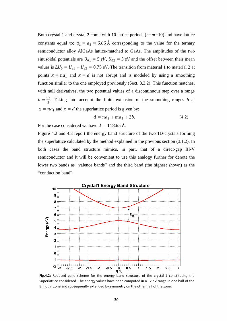
Both crystal 1 and crystal 2 come with 10 lattice periods (n=m=10) and have lattice
constants equal to: corresponding to the value for the ternary
semiconductor alloy AlGaAs lattice-matched to GaAs. The amplitudes of the two
sinusoidal potentials are , and the offset between their mean
values is . The transition from material 1 to material 2 at
points and is not abrupt and is modeled by using a smoothing
function similar to the one employed previously (Sect. 3.3.2). This function matches,
with null derivatives, the two potential values of a discontinuous step over a range
. Taking into account the finite extension of the smoothing ranges b at
and the superlattice period is given by:
(4.2)
For the case considered we have .
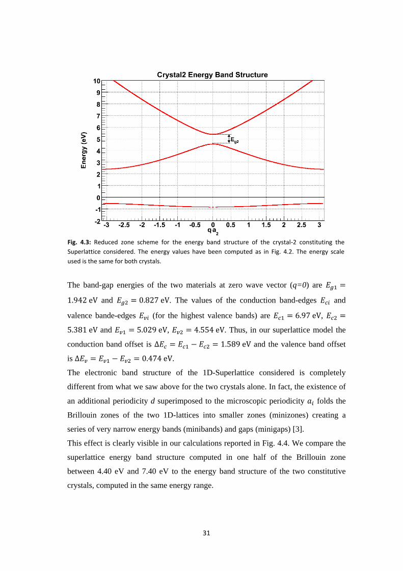
Figure 4.2 and 4.3 report the energy band structure of the two 1D-crystals forming
the superlattice calculated by the method explained in the previous section (3.1.2). In
both cases the band structure mimics, in part, that of a direct-gap III-V
semiconductor and it will be convenient to use this analogy further for denote the
lower two bands as “valence bands” and the third band (the highest shown) as the
“conduction band”.
Fig.4.2: Reduced zone scheme for the energy band structure of the crystal-1 constituting the
Superlattice considered. The energy values have been computed in a 12 eV range in one half of the
Brillouin zone and subsequently extended by symmetry on the other half of the zone.
31
The band-gap energies of the two materials at zero wave vector (q=0) are
and . The values of the conduction band-edges and
valence bande-edges (for the highest valence bands) are ,
and , . Thus, in our superlattice model the
conduction band offset is and the valence band offset
is .
The electronic band structure of the 1D-Superlattice considered is completely
different from what we saw above for the two crystals alone. In fact, the existence of
an additional periodicity d superimposed to the microscopic periodicity folds the
Brillouin zones of the two 1D-lattices into smaller zones (minizones) creating a
series of very narrow energy bands (minibands) and gaps (minigaps) [3].
This effect is clearly visible in our calculations reported in Fig. 4.4. We compare the
superlattice energy band structure computed in one half of the Brillouin zone
between 4.40 eV and 7.40 eV to the energy band structure of the two constitutive
crystals, computed in the same energy range.
Fig. 4.3: Reduced zone scheme for the energy band structure of the crystal-2 constituting the
Superlattice considered. The energy values have been computed as in Fig. 4.2. The energy scale
used is the same for both crystals.
32
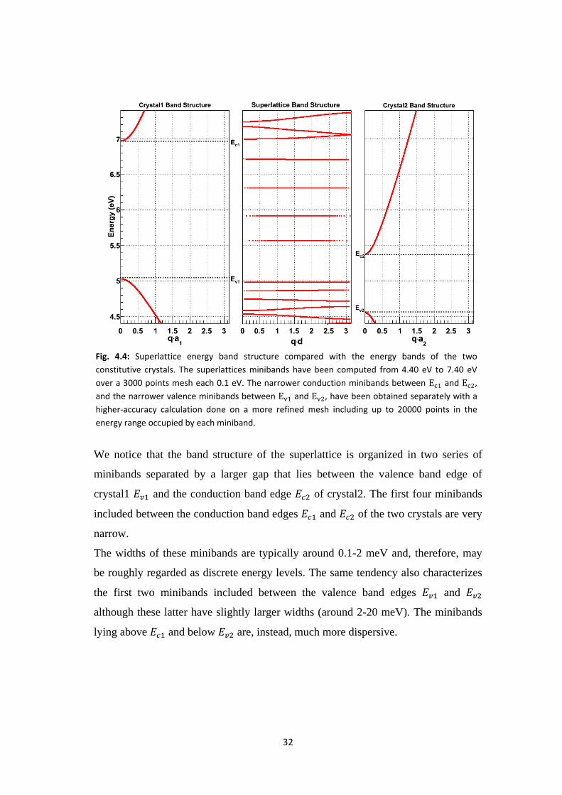
We notice that the band structure of the superlattice is organized in two series of
minibands separated by a larger gap that lies between the valence band edge of
crystal1 and the conduction band edge of crystal2. The first four minibands
included between the conduction band edges and of the two crystals are very
narrow.
The widths of these minibands are typically around 0.1-2 meV and, therefore, may
be roughly regarded as discrete energy levels. The same tendency also characterizes
the first two minibands included between the valence band edges and
although these latter have slightly larger widths (around 2-20 meV). The minibands
lying above and below are, instead, much more dispersive.
Fig. 4.4: Superlattice energy band structure compared with the energy bands of the two
constitutive crystals. The superlattices minibands have been computed from 4.40 eV to 7.40 eV
over a 3000 points mesh each 0.1 eV. The narrower conduction minibands between and ,
and the narrower valence minibands between and , have been obtained separately with a
higher-accuracy calculation done on a more refined mesh including up to 20000 points in the
energy range occupied by each miniband.
33
These trends are also reflected in the 1D-DoS reported in Fig. 4.5. We see that the
DoS of the minibands between and resembles a delta function as expected
for discrete energy levels.
4.2 Superlattice Bloch wavefunctions
The Superlattice Bloch wavefunctions have been computed numerically integrating
Eq. (3.1) with the superlattice potential in Fig. 4.1 for given energy values as
explained in sect. 3.2.
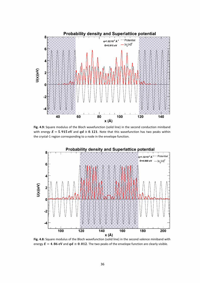
Figures from 4.6 to 4.9 report the square modulus of the Bloch wavefunctions
computed in the first two conduction minibands with energies (Fig.
4.6) and (Fig. 4.8), and in the first two valence minibands with
energies (Fig. 4.7) and (Fig. 4.9). We have chosen to
compute only the wavefunctions with nearly zero wave-vectors because those having
Fig. 4.5: Superlattice 1D-DoS compared with the 1D-DoS of the two constitutive crystals. The 1D-
DoS values have been computed from 4.40 eV to 7.40 eV over the same energy mesh used in Fig.
4.4. to obtain the energy bands.

34
exact wave-vectors cannot be obtained with our numerical method due to the
lack of a precise evaluation of the energy values at these stationary points. However,
this fact is not as relevant as it might seem. Indeed, we have verified that for energies
in the narrower minibands is nearly independent of the wave-vector value.
This independence is lost, instead, in much more dispersive minibands (such as the
minibands lying above and below ) where computed with
behaves differently from computed with (see Fig 4.10 and 4.11).
A common feature of the computed Bloch wavefunctions, shown in the following
figures, is their rapidly oscillating behavior enveloped by a slowly varying function
on the scale of the lattice constant of the constitutive crystals. The number of nodes
of this envelope function increases as higher-energy states in the conduction
minibands or lower-energy states in the valence minibands are considered: this can
be seen comparing Fig. 4.6 to 4.8, and Fig. 4.7 to 4.9.
Fig. 4.6: Square modulus of the Bloch wavefunction (solid line) in the first conduction miniband with
energy and . The square modulus is plotted in a unit cell shifted from
to centered around the crystal-2 (white) region. The computed values have been
normalized in order to be displayed on the same scale of the superlattice potential (dashed line).

35
Another interesting aspect of these states is their localization in different regions of
the superlattice potential. In particular, the wavefunctions in the narrow conduction
minibands (Fig. 4.6 and 4.8) are localized in crystal1 regions while the
wavefunctions in the narrow valence minibands (Fig. 4.7 and 4.9) are localized in
crystal2 regions.
This fact confirms that the first conduction and valence minibands behave as discrete
energy levels in a quantum well. To be more precise we can say that crystal1 acts as
a quantum well for particles occupying Bloch states in the narrower conduction
minibands and crystal2, instead, acts as a quantum well for particles occupying
Bloch states in the narrower valence mini-bands. This behavior is also found in real
hetero-crystalline superlattices where (as seen in sect. 2.2) a material can act as a
quantum well for electrons in the conduction band and, at the same time, as a barrier
for holes in the valence band. So, from this point of view, our 1D- model may be
regarded as a type-II staggered superlattice.
Fig.4.7: Square modulus of the Bloch wavefunction (solid line) in the first valence miniband with
energy and . In this case the wavefunction is plotted in a shifted unit
cell centered around the crystal-1 (grey shaded) region from to .
36
Fig. 4.8: Square modulus of the Bloch wavefunction (solid line) in the second valence miniband with
energy and . The two peaks of the envelope function are clearly visible.
Fig. 4.9: Square modulus of the Bloch wavefunction (solid line) in the second conduction miniband
with energy and . Note that this wavefunction has two peaks within
the crystal-1 region corresponding to a node in the envelope function.
37
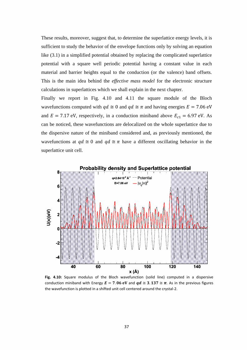
These results, moreover, suggest that, to determine the superlattice energy levels, it is
sufficient to study the behavior of the envelope functions only by solving an equation
like (3.1) in a simplified potential obtained by replacing the complicated superlattice
potential with a square well periodic potential having a constant value in each
material and barrier heights equal to the conduction (or the valence) band offsets.
This is the main idea behind the effective mass model for the electronic structure
calculations in superlattices which we shall explain in the next chapter.
Finally we report in Fig. 4.10 and 4.11 the square module of the Bloch
wavefunctions computed with and and having energies
and , respectively, in a conduction miniband above . As
can be noticed, these wavefunctions are delocalized on the whole superlattice due to
the dispersive nature of the miniband considered and, as previously mentioned, the
wavefunctions at and have a different oscillating behavior in the
superlattice unit cell.
Fig. 4.10: Square modulus of the Bloch wavefunction (solid line) computed in a dispersive
conduction miniband with Energy and . As in the previous figures
the wavefunction is plotted in a shifted unit cell centered around the crystal-2.

38
Fig. 4.11: Square modulus of the Bloch wavefunction (solid line) computed in a dispersive
conduction miniband with Energy and The wavefunction
oscillates differently from that in Fig. 4.10 especially in the crystal-2 region (grey shaded).
39
5 The effective mass approximation in hetero-
crystalline superlattices
5.1 Brief summary on superlattice electronic structure
methods
Real hetero-crystalline superlattices can be much more complex systems than the
simple one dimensional model previously considered.
The study of the electronic structure in these systems require appropriate theoretical
approaches. The degree of complexity in these approaches ranges from simple
empirical methods to self-consistent many-electrons ab-initio calculations.
In empirical methods the electronic structure of the materials is described by a bulk
model having parameters which do not change when the constituent materials are
combined to form the superlattice. In addition to the bulk parameters, extra
parameters are needed to describe the interfaces. Empirical methods are usually
divided in supercell approaches and boundary-condition approaches. In supercell
approaches the superlattice is described by a Hamiltonian having a large unit cell; its
eigenfunctions are found by conventional band-structure methods. Because of the
rapid increase in computational cost with layer thickness, these methods are
restricted only to thin-layer superlattices. In boundary-condition approaches, instead,
the eigenfunctions of the superlattice Hamiltonian are determined by matching the
bulk wavefunctions at the interfaces. Empirical-tight-binding [14, 15] and
pseudopotentials [16] calculations have been applied both in supercells and boundary
condition approaches.
Ab-initio methods are usually based on self-consistent many-electron calculations
such as self-consistent pseudopotentials and Density-Funcitonal-Theory in Local-
Density-Approximation (LDA-DFT). All these methods use supercell approaches
and are restricted to the studies of ground-state properties of the interfaces (e.g.
valence band offsets) and the electronic structure of thin-layer superlattices.
Reference [17] provides a complete survey on superlattice electronic-structure
theoretical techniques and the main related works.
40
In the next section we shall focus on one of the simplest methods for superlattice
electronic structure calculations: the Effective Mass Approximation (EMA),
sometimes also called the envelope function model. Although this approach was
initially developed to describe the electronic motion in the presence of slowly
varying perturbations in the crystalline potential [18, 19], since the advent of
semiconductor heterostructures it has been widely applied to these systems as well,
even though the use of the EMA is much more difficult to justify in this case [20]. In
this context the EMA can be viewed as a boundary-condition method because it
requires wave-function matching at superlattices interfaces.
The EMA has some advantages as compared to pseudo-potential or tight-binding
calculations: it is relatively simple and easy to implement; input parameters (such as
zone-center band energies, momentum matrix elements, etc.) are well known and the
dependence of the results on these input parameters is direct and easy to understand.
The first theoretical efforts to describe superlattices and heterostructures in the EMA
were based on Kronig-Penney-type models scaled by bulk effective masses and
energy-band offsets [5, 6]. These simple models are also called one-band effective
mass models because they do not include coupling between different bulk energy
bands by the superlattice potential.
Scaled Kronig-Penney-models are particularly useful in predicting zone center
energies in type-I superlattices made from relatively wide-band-gap semiconductors,
such as GaAs\Ga1-xAlxAs superlattices. They are not appropriate, however, for
superlattices in which there is extensive band mixing, such as the type-II superlattice
InAs/GaSb. In these cases better results are provided by a multiband-effective mass
model, such as the two-band model developed by Bastard [21, 22] and White and
Sham [23], which can account for mixing between the conduction and valence band
states.
Effective-mass models can be also adjusted to include the stress effects in strained
layer superlattices (SLS) and the charging effects in doping superlattices. To describe
charging accurately, however, self consistent calculations are required.
41
5.2 One-Band effective mass model
In this section we describe a simple one-band effective mass model for the electronic
structure calculations in hetero-crystalline superlattices. This model assumes:
flat band conditions and mathematically abrupt interfaces, i.e., there is an
abrupt change in the underlying crystalline properties at the heterojunction
with no charging effects and no band bending;
perfect lattice matching and same crystallographic structure for the A and B
materials constituting the superlattice layers, i.e. no strain effects;
a shallow and piecewise constant superlattice potential in each layer. This is
a key-hypothesis to apply the effective mass approximation and in a
superlattice it can be considered correct only if the layers are thick enough.
Moreover we will suppose that:
the superlattice potential does not mix conduction and valence-edge band
states but only shifts them, which is plausible due to the different symmetries
of conduction and valence bands;
the coupling between states within the same band but in different valleys, can
be neglected.
Regarding the latter assumption it may be considered correct only in
heterostructures where A and B constituent materials have similar Bloch functions in
a neighborhood of the same band-edge. This is a good approximation for the
conduction-band edges states in type-I GaAs/GaAlAs superlattices but not in type-II
GaAs/GaAlAs superlattices with GaAs layers thinner than 2nm. Here it becomes
important to consider a strong intra-band coupling [21] and a multi-band
effective mass model is required. In the following discussion, however, we shall
restrict our considerations only to the -related conduction-band edges with
isotropic effective masses. In practice we assume that the superlattice potential can
couple the Bloch states only around the -conduction-band edge.
Bearing these assumptions in mind our starting point is the well-established
effective-mass approximation for bulk semiconductors. Consider an electron moving
in a bulk semiconductor under the influence of an additional slowly varying potential
. It is possible to prove that in a one-band approximation and for energies, ,
42
close to the band edge at , the wave function, , of a perturbed electronic
state can be approximately written as [7]:
(5.1)
where is the periodic part of the Bloch function at in the considered
nth-band and is known as the envelope function and can be regarded as a
slowly varying modulation of the rapidly varying band-edge Bloch function.
Moreover it can be shown that the electron envelope function, , satisfies an
equation similar to the Schrödinger equation:
(5.2)
where is the band-edge energy and is the isotropic effective mass.
Now consider the case of a superlattice formed by two different semiconductor
materials A and B. According to the previous discussion (Sect. 2.2), within the flat
band model and the abrupt interfaces approximation, an electron in the conduction
band feels an additional potential along the growth direction, z, due to the conduction
band-edges offset. If the A and B layers are thick enough this potential can
reasonably supposed to be slowly varying within each one of the bulk materials. In
the simplest situation the confining potential is square-well like:
(5.3)
where
is the energy shift (i.e. the band offset) between the
conduction band edges at going from the A to the B material (with
,
as in Fig.2.4).
In each of the A and B layers an equation like (5.2) holds:
(5.4)
where A, B suffixes denote if is in A or B layer and the potential has the
form (5.3). Note that in (5.3) we are considering the energy of the conduction band-
edge in the A layer as the reference for the energies of the conduction electrons in
the superlattice potential, i.e. .
Since the confinement potential depends on z only
can be factorized
into
43
(5.5)
where S is the sample area and is a bi-dimensional wave-vector which
is the same in the planes perpendicular to the growth direction due to the assumption
of identical lattice constants in the A and B layers.
Substituting (5.5) in (5.4) we obtain the following equation:
(5.6)
Introducing a position dependent effective mass,
(5.7)
equation (5.6) can be generalized in the whole heterostructure as
(5.8)
where we have replaced the non-Hermitian kinetic energy operator
with an Hermitian one:
Equation (5.8) is known as the Ben Daniel-Duke equation and it is the starting point
to calculate the electronic states of superlattices or, more generally, of any other
heterostructure in a one-band effective mass model.
It is worth emphasizing, however, that the derivation given above for the Ben Daniel-
Duke equation cannot be considered completely rigorous. The main problem is the
heuristic nature of the effective mass approximation, i.e. the lack of a derivation that
starts from the microscopic Schrodinger equation and at each stage provides a means
of estimating the error in any approximation made [20]. Moreover, since a
momentum operator p and a position-dependent effective mass do not
commute, a question concerning the correct form of the kinetic operator has arisen.
This question is also directly related to the form of the boundary conditions to
impose on the envelope functions at abrupt material interfaces.
44
A wide range of theoretical approaches have been taken to determine the appropriate
boundary conditions to impose at abrupt interfaces. However, the most common
choice is
(5.9)
These boundary conditions are best known as Ben Daniel-Duke Boundary
Conditions. The continuity of at interfaces derives from the continuity
assumption on the total wave-function, , and from the identity assumption for
the periodic part of the band-edge Bloch functions in each A and B layer of the
heterostructure:
(5.10)
The usual way of justifying the continuity of
, instead, is to appeal to
conservation of the probability current,
across the interfaces [21].
If the continuity of is assumed, then continuity of
will ensure current
conservation. Another way to derive the continuity of
is to integrate the (5.8)
across an interface. However, this approach depends on the form chosen for the
kinetic energy operator. In particular, it has been proved that any combination of
linear momentum operators and effective masses of the form (see e.g. Ref. [24])
will also satisfy Eq. (5.9). The accepted choice is and but clearly
there are infinitely many solutions.
These approaches for justifying the boundary conditions, however, suffer of two
major drawbacks. On one hand, they are only applicable in heterostructures having
non-degenerate band edges with similar band-edge Bloch functions in each A and B
layer [25]. On another hand, the assumption (5.10) is not consistent with the use of
different bulk parameters for the constituent materials, such as two different effective
masses in A and B layers, which imply different momentum matrix element between
the zone-center Bloch functions [17].
Despite these inconsistencies and the lack of a rigorous justification the one-band
effective mass approximation, seems to work well at least for the lowest conduction
45
states of GaAs/Ga1-xAlxAs superlattices with and GaAs layer
thickness larger than . In these cases both constituent materials have direct
band gaps, the band profiles are type-I and the two materials are closely lattice
matched. As a result of these simplifying features, there is little mixing of constituent
materials bands and a simple effective mass model based on the equation (5.8)
provides a fairly good description of the zone center energy levels.
5.3 Result on superlattice minibands and 3D-Density of States
As we have seen in the previous section in a one-band effective-mass model, the 3D-
electronic motion in the superlattice can be separated in a 2D-motion in the layer
planes and in a 1D-motion along the superlattice growth direction. Since in the
effective mass approximation we restrict to consider energies lying in a
neighborhood of a non-degenerate zone-centre conduction band minimum, the 2D-
motion in the layer planes can be regarded appropriately as the motion of a free
particle having a mass equal to the effective mass at the conduction band-edge in the
layer considered. The 1D-motion along the growth direction, instead, is affected by
the superlattice confining potential and it’s similar to the motion of a particle in a
1D-periodic potential having different masses in the two A and B materials
constituting the superlattice.
The energies and the envelope-wavefunctions of the electrons in the
superlattice potential are determined by Eq.(5.8). In the simple case of a constant
effective mass, i.e. (which is a good approximation at least for
GaAs/Ga1-xAlxAs superlattices with ) the wave equation (5.8)
becomes similar to an one-dimensional Schrödinger equation:
(5.11)
where we have defined:
(5.12)
and is the periodic confinement square well potential (5.3) having a period d
typically 10-20 times larger than the lattice constant of the superlattice constitutive
46
materials. As we have seen in sect. 3.1, a complete set of solutions of (5.11) exist in
Bloch’s form. Thus, to conform to the previous notation we will denote the wave-
vector along the z direction as q and we will use an m-index to distinguish between
superlattice Bloch-states having the same wave-number but belonging to different
energy minibands.
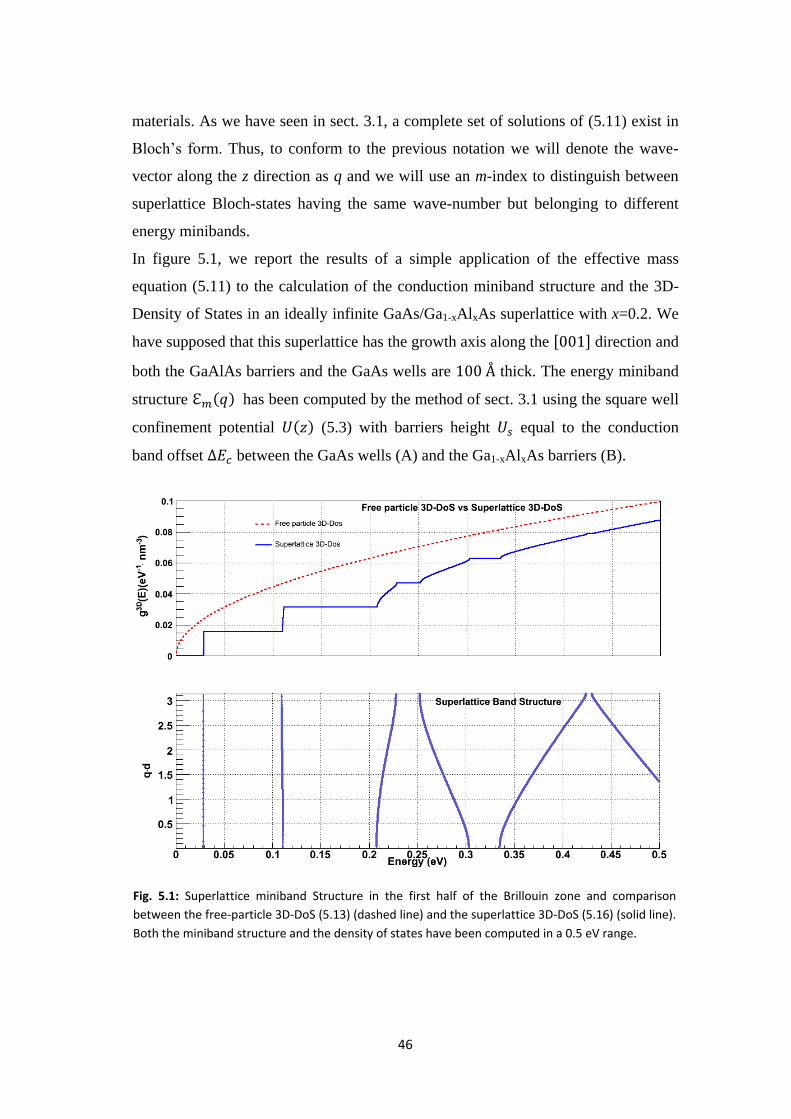
In figure 5.1, we report the results of a simple application of the effective mass
equation (5.11) to the calculation of the conduction miniband structure and the 3D-
Density of States in an ideally infinite GaAs/Ga1-xAlxAs superlattice with x=0.2. We
have supposed that this superlattice has the growth axis along the direction and
both the GaAlAs barriers and the GaAs wells are thick. The energy miniband
structure has been computed by the method of sect. 3.1 using the square well
confinement potential (5.3) with barriers height equal to the conduction
band offset between the GaAs wells (A) and the Ga1-xAlxAs barriers (B).
Fig. 5.1: Superlattice miniband Structure in the first half of the Brillouin zone and comparison
between the free-particle 3D-DoS (5.13) (dashed line) and the superlattice 3D-DoS (5.16) (solid line).
Both the miniband structure and the density of states have been computed in a 0.5 eV range.
47
The experimental value for x=0.2 is [6] where is the
difference between the band-gap energies of the two semiconductor materials:
Since the measured band-gap energy in is
and the band-gap energy in is experimentally described by a linear
function of the composition [26]
we have, for x=0.2, . Regarding the effective mass used in
the calculations, it has been set equal to the mean value between the electron
effective mass in GaAs and the electron effective mass in Ga1-
xAlxAs. The latter depends linearly on the alloy composition [26]:
so, for x=0.2, the effective mass mean value is .
As can be noticed in Fig. 5.1, the superlattice potential also produces a significant
change in the 3D-Density of States compared to what we have in an homogeneous
semiconductor for energies in a neighborhood of a zone-centre conduction band
minimum. In this case the 3D-DoS (per unit volume) can be well approximated by
the 3D-DoS of a free particle having a mass equal to the effective mass at the
band-edge considered:
(5.13)
In a superlattice, instead, the 3D-DoS is determined by considering the contributions
both from the energy miniband structure and the free particle motion in the layer
planes. In particular, the 3D-DoS (per unit volume, V) is given by:
(5.14)
where the factor 2 accounts for the two-fold spin degeneracy of the superlattice
electronic states identified by the three indices and having energy:
(5.15)
Substituting (5.15) in (5.14) it’s straightforward to show that the superlattice 3D-DoS
can be expressed as:
48
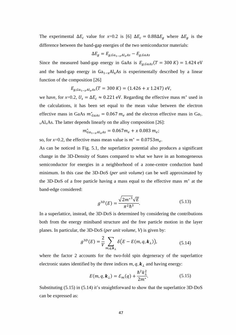
(5.16)
where is a unit step function which is unit if and the integration is
performed only on one half of the superlattice Brillouin zone (along the z-direction)
due its inversion symmetry. In general each miniband has a finite energy width when
q describes the first-half of the Brillouin zone: . So, for
, while for is constant:
Within an allowed miniband , instead, is given by:
where is the wave-vector in the miniband dispersion curve. Taking into account
these results we have computed the superlattice 3D-DoS (blue solid line in the figure
5.1) varying the energy on a given range and evaluating for each miniband.
Adding up all band-contributions we have obtained, as can be noticed, a 3D-DoS that
has a step-like character with plateau-values at integer multiples of
when E falls
inside the minigaps of the superlattice energy dispersion relation It is noteworthy
that the superlattice 3D-DoS, unlike the free-particle 3D-DoS, has singularities in its
derivatives at the points corresponding to three-dimensional minima where
and to saddle points where
Another interesting aspect that can be inferred both from the superlattice 3D-DoS
and the miniband structure is that the lower energy minibands are very narrow and
resembles discrete energy levels in a quantum well, just like we have seen previously
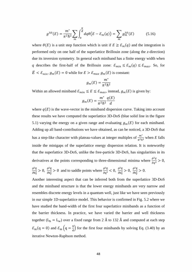
in our simple 1D-superlattice model. This behavior is confirmed in Fig. 5.2 where we
have studied the band-width of the first four superlattice minibands as a function of
the barrier thickness. In practice, we have varied the barrier and well thickness
together ( ) over a fixed range from 2 to 132 and computed at each step
and
for the first four minibands by solving Eq. (3.40) by an
iterative Newton-Raphson method.
49
The shaded area between the two limit curves and
describes the allowed energy values in each miniband. As can be noticed for
the first two minibands are very narrow and coincide nearly with
the energy levels calculated in a single quantum well having width and
height equal to the conduction band offset .
Figure 5.2 also clearly shows how the isolated energy levels evolve into energy
minibands when the wells separation and the barriers thickness are decreased. As a
consequence in this situation the tunneling coupling among the wells increase and
the isolated quantum wells structure becomes a superlattice.
Fig. 5.2: First four allowed energy conduction minibands in a superlattice
(x=0.2) calculated as a function of the well/barrier width ( ). The solid lines represent the
energy levels of a single quantum well as a function of the well/barrier width. The quantum well
energy levels have been computed by solving for each value the following transcendental
equations [26]:
for even-parity states and
for odd-parity states with and defined as in Eq. (3.39).
50
6 Discussion and Conclusions
In the present thesis we have studied the electronic structure of a 1D-superlattice
model by implementing (and testing) a simple numerical method to solve a one-
dimensional time-independent Schrödinger equation in any arbitrary “smooth”
periodic potential. Despite its simplicity this method allowed us to obtain accurately
the superlattice energy minibands, the Bloch wavefunctions and the 1D-DoS.
In our numerical calculations we found that there may be Bloch states “localized” in
different crystalline regions of the superlattice. The localized Bloch states have
energies in the narrower minibands and show a characteristic rapidly oscillating
behavior enveloped by a slowly varying function that resembles closely an energy
eigenfunction in a quantum well. We also noticed that the same material can behave
either as a well or as barrier for the electrons depending on the energy of the
occupied Bloch states, i.e. if their energy lies in a narrower miniband between the
conduction band-edges or in a narrower miniband between the valence band-edges of
the two constitutive materials. Moreover, the results obtained suggest that, to
determine the superlattice electronic structure, an even simpler method may be used.
This method is the Effective Mass Approximation (EMA) and consists in studying the
behavior of the envelope functions only, by solving a Schrödinger-like equation in a
simplified square well periodic potential having a constant value in each layer and
barrier heights equal to the conduction/valence band offset. Although in real
superlattices the EMA is difficult to justify and is not entirely rigorous, it returns
correct results at least for the conduction miniband states in GaAs/Ga1-xAlxAs
superlattices with . In particular, in this case a simple one-band
effective mass model provides a fairly good description of the zone center energy
levels. We applied this model to study the electronic miniband structure and the 3D-
DoS in a ideally infinite GaAs/Ga1-xAlxAs superlattice with having both Ga1-
xAlxAs barriers and GaAs wells thick. We noticed that the superlattice
confining potential produces significant changes in the 3D-DoS as compared to the
3D-DoS of a 3D-isotropic system (free particle). The superlattice 3D-DoS has a step-
like character with plateau-values corresponding to the energies in the minigaps of

51
the energy dispersion relation. Moreover, we also showed that the narrow
superlattice energy minibands coincide with the discrete energy levels in an isolated
quantum well and that they evolve into more dispersive minibands decreasing the
barriers/well thickness.
The latter result proves that the properties (width, position,..etc.) of the minibands
and corresponding minigaps in a superlattice are strongly influenced by the size of
the barrier/well materials. Therefore, by precisely modulating these parameters
during the epitaxial growth processes, the electronic structure can be artificially
controlled creating predesigned band profiles and energy levels. The flexibility in the
electronic properties that is introduced by this design possibility makes superlattices
useful in multiple technological applications, ranging from optoelectronics (infrared
detectors, electro-optic modulators, quantum semiconductor lasers, high-efficiency
solar cells..ecc.) to the telecommunications.
Moreover superlattices and similar layered structures present a unique opportunity to
study novel quantum phenomena over a new length scale which is intermediate
between that of atomic systems and that of macroscopic (bulk) materials. Such
phenomena include resonant electron tunneling, Tamm surface states, negative
differential resistivity, electric-field-induced quantization effects such as Wannier-
Stark ladders and Bloch oscillations all of which may be modeled as 1D-quantum-
mechanical problems [27].
A natural extension of the work presented in this thesis would be to develop a more
accurate electronic-structure calculation in a tight-binding or a pseudopotential
approach and compare its results with those obtained in a effective mass model.
It would be also interesting to investigate the formation of an energy band structure
in a realistic finite-size superlattice. Here, the 1D-confining potential cannot be
considered infinitely periodic and a different numerical technique (as it could be a
shooting method [11]) is required to calculate the superlattice energy levels in the
context of a simple one-band effective-mass approximation [26, 30].
In this context, further developments could include the study of the formation of
surfaces states and the influence of an electric field on the superlattice energy band
structure with the previously mentioned quantum phenomena.
52
References
[1] W. J. Choyke, D. R. Hamilton, and P. Lyle, Phys. Rev., 133, A1163, 1964.
[2] H. Sato and R. S. Toth, Phys. Rev., 124, 1833, 1961.
[3] L. Esaki and R. Tsu, IBM J. Res. Devel., 14, 61, 1970.
[4] L.L. Chang, L. Esaki, W. E. Howard, and R. Ludeke, J. Vac. Sci. Technol., 10, 11, 1973.
[5] D. Mukherji and B. R. Niag, Phys. Rev. B, 12, 4438, 1975.
[6] R. Dingle, W. Wiegmann, and C. H. Henry, Phys. Rev. Lett., 33, 827, 1974.
[7] M. Cardona and Peter Y. Yu, Fundamentals of Semiconductors, Fourth Edition, Springer.
[8] F. Bloch, Z. Phys., 52, 555, 1929.
[9] W. Magnus and S. Winkler, Hill's Equation, New York, Dover Phoenix Editions, 1979.
[10] Richard J. Gonsalves, (2011) Computational Physics I,
http://www.physics.buffalo.edu/phy410-505/2011/topic2/app3/index.html
[11] W. H. Press, S.A. Teukolsky, W.A. Vetterling, and B.P. Flannery, Numerical Recipes in C. The art
of Scientific Computing, Second Edition, Cambridge University Press, 1992.
[12] N.W. Ashcroft and N.D. Mermin, Solid state physics, Saunders College Pub., 1976.
[13] P. Hadley, (2011) Molecular and Solid state Physics,
http://lamp.tu-graz.ac.at/~hadley/ss1/bands/bands.php
[14] J. N. Schulmann and T. C. McGill, Phys. Rev. Lett. , 39, 1680, 1977.
[15] J. N. Schulmann and Yia-Chung Chang, Phys. Rev. B, 24, 4445, 1981.
[16] M. Jaros, K. B. Wong, and M. A. Gell, Phys. Rev. B, 31, 1205, 1985.
[17] C. Mailhiot and D. L. Smith, Rev. Mod. Phys., 62, 173, 1990.
[18] J. C. Slater, Phys. Rev., 76, 1592, 1949.
[19] J.M. Luttinger and W. Kohn, Phys. Rev., 97, 869, 1955.
[20] M. G. Burt, J. Phys.: Condens. Matter, 4, 6651, 1992.
[21] G. Bastard, Wave Mechanics Applied to Semiconductor Heterostructures, France, Ies Editions De
Physique.
[22] G. Bastard, Phys. Rev. B, 24, 5693, 1981.
[23] S. R. White and L. J. Sham, Phys. Rev. Lett., 47, 879, 1981.
[24] R. A. Morrow and K. R. Browstein, Phys. Rev. B, 30, 678, 1984.
[25] L. J. Sham and G. T. Einevoll, Phys. Rev. B, 49, 10533, 1993.
[26] P. Harrison, Quantum Wells, Wires and Dots, Second Ed., Wiley, 2005.
[27] L. Esaki, Physica Scripta, T42, 102, 1992.
[28] H.T. Grahn, Semiconductor Superlattices: Growth and Electronic Properties, World Scientific,
1995.
[29] J.H. Davies, The Physic of Low Dimensional Semiconductors, Cambridge Univ. Press, 1998.
[30] S. F.-P. Paul and H. Fouckhardt, Phys. Lett. A, 286, 199, 2001.