Embed Size (px)
Citation preview

Electronic Structure of Heterogeneous MaterialsApplication to Optical properties
Natália Leitão Marques Morais
Thesis to obtain the Master of Science Degree in
Engineering Physics
Supervisor: Prof. Dr. José Luís Rodrigues Júlio Martins
Examination Committee
Chairperson: Prof. Dr. Pedro Domingos Santos do SacramentoSupervisor: Prof. Dr. José Luís Rodrigues Júlio MartinsMember of the Committee: Prof. Dr. Eduardo Filipe Vieira de Castro
October 2014

ii

Acknowledgments
I would like to thank the Instituto de Engenharia de Sistemas e Computadores, Microsistemas & Nan-
otecnologias (INESC-MN) of Lisbon, that very kindly hosted me in as I predict to be the beginning of my
career as a researcher in Physics, subject that I’ve always been passionate about since at a very young
age.
I would like to thank my coordinator Jose Luıs Martins for guiding me on this project that concluded
this Mestrado em Engenharia Fısica Tecnologica (MEFT) 5 years Master Instituto Superior Tecnico (IST,
Lisbon) program and providing me an opportunity to perform a high-quality research in the domain of
Condensed Matter Physics and also to his research fellow Carlos Reis who provided me some other
help I needed.
iii

iv

Resumo
O objectivo teste projecto e encontrar uma descricao para um solido cristalino de elementos de grupo
IV Silıcio, Carbono e Germanio, e calcular a estrutura electronica e propriedades opticas. Para calcu-
lar a estrutura de bandas vao se usar pseudopotenciais. Vai ser usado o Metodo de Pseudopotencial
Empırico (EPM) para encontrar o melhor ajuste dos pseudopotenciais aos dados experimentais con-
hecidos da estrutura de bandas de cada um destes elementos. Antes disso, comeca-se por ajustar
os pseudopotenciais a um gerador de pseudopotenciais ab initio, para que se encontre uma regiao
aceitavel de parametros dos pseudopotencias empıricos. A partir daı, melhora-se o ajuste dos poten-
ciais a experiencia. As propriedades opticas dos cristais de Si, C e Ge sao calculadas. Com estes
pseudopotenciais, o objectivo e de gerar um pseudopotencial para cada um destes elementos que
simule correctamente as propriedades, que depois seja transferıvel para super-redes de Si-Ge-C. O
objectivo final e prever o comportamento de nano-estruturas de Si-Ge-C.
Palavras-chave: Nanotecnologias, Simulacao de Materiais, Fısica da Materia Condensada,
Aplicacoes de Fısica do Estado Solido, Pseudopotenciais, Propriedades Opticas
v

vi

Abstract
The objective of this work is to find a description of the group IV elements Silicon, Carbon and Germa-
nium and calculate the electronic structure and optical properties of materials containing those elements.
To calculate the band structure we will use pseudopotentials. We will use an Empirical Pseudopotential
Method to find the better fitting to the pseudopotentials to the experimental known data about the band
structure to each of this elements. We start by fitting the pseudopotentials to an ab initio pseudopotential
generator, to find the first acceptable set of pseudopotentials’ parameters. From that we further adjust
the potentials to the experiment, and find a better fit. After that the optical properties of the bulk Si,
C and Ge are calculated. The purpose is to generate a pseudopotential to each of this elements that
simulates correctly the properties and can be transferable to supercells of Si-Ge-C. We want to predict
the behaviour of Si-Ge-C nanostructures.
Keywords: Nanotechnologies, Simulation of Materials, Condensed Matter Physics, Solid State
Applications, Pseudopotentials, Optical Properties
vii

viii

Contents
Acknowledgments . . . . . . . . . . . . . . . . . . . . . . . . . . . . . . . . . . . . . . . . . . . iii
Resumo . . . . . . . . . . . . . . . . . . . . . . . . . . . . . . . . . . . . . . . . . . . . . . . . . v
Abstract . . . . . . . . . . . . . . . . . . . . . . . . . . . . . . . . . . . . . . . . . . . . . . . . . vii
List of Tables . . . . . . . . . . . . . . . . . . . . . . . . . . . . . . . . . . . . . . . . . . . . . . xii
List of Figures . . . . . . . . . . . . . . . . . . . . . . . . . . . . . . . . . . . . . . . . . . . . . xvii
1 Introduction 1
1.1 Motivation . . . . . . . . . . . . . . . . . . . . . . . . . . . . . . . . . . . . . . . . . . . . . 1
1.2 State-of-the-art . . . . . . . . . . . . . . . . . . . . . . . . . . . . . . . . . . . . . . . . . . 2
1.2.1 Si, Ge and C . . . . . . . . . . . . . . . . . . . . . . . . . . . . . . . . . . . . . . . 2
1.2.2 Group IV Semiconductor Compounds and Alloys . . . . . . . . . . . . . . . . . . . 3
1.3 Thesis Outline . . . . . . . . . . . . . . . . . . . . . . . . . . . . . . . . . . . . . . . . . . 11
2 Theoretical Introduction 12
2.1 The many-body problem . . . . . . . . . . . . . . . . . . . . . . . . . . . . . . . . . . . . . 12
2.2 The Adiabatic Approximation . . . . . . . . . . . . . . . . . . . . . . . . . . . . . . . . . . 13
2.3 Separable Schrodinger equation . . . . . . . . . . . . . . . . . . . . . . . . . . . . . . . . 14
2.4 The Hartree-Fock Method . . . . . . . . . . . . . . . . . . . . . . . . . . . . . . . . . . . . 14
2.5 Density Functional Theory . . . . . . . . . . . . . . . . . . . . . . . . . . . . . . . . . . . . 16
2.6 Hohenberg-Kohn Theorem . . . . . . . . . . . . . . . . . . . . . . . . . . . . . . . . . . . 18
2.7 Kohn-Sham Equations . . . . . . . . . . . . . . . . . . . . . . . . . . . . . . . . . . . . . . 19
2.8 Pseudopotentials . . . . . . . . . . . . . . . . . . . . . . . . . . . . . . . . . . . . . . . . . 21
2.8.1 Ab initio pseudo-potentials . . . . . . . . . . . . . . . . . . . . . . . . . . . . . . . 21
2.8.2 Empirical Pseudopotential methods . . . . . . . . . . . . . . . . . . . . . . . . . . 23
2.8.3 Non-local and Spin-Orbit Pseudopotentials . . . . . . . . . . . . . . . . . . . . . . 25
2.9 Screening . . . . . . . . . . . . . . . . . . . . . . . . . . . . . . . . . . . . . . . . . . . . . 29
2.9.1 Definitions of the dielectric function . . . . . . . . . . . . . . . . . . . . . . . . . . . 29
2.9.2 Screening in a metal . . . . . . . . . . . . . . . . . . . . . . . . . . . . . . . . . . . 30
2.10 Optical properties . . . . . . . . . . . . . . . . . . . . . . . . . . . . . . . . . . . . . . . . 32
2.11 Imaginary part of the dielectric function ε2 . . . . . . . . . . . . . . . . . . . . . . . . . . . 33
ix

3 Results 36
3.0.1 Simple test: free electron . . . . . . . . . . . . . . . . . . . . . . . . . . . . . . . . 36
3.1 Silicon . . . . . . . . . . . . . . . . . . . . . . . . . . . . . . . . . . . . . . . . . . . . . . . 37
3.1.1 Description only with a local pseudopotential . . . . . . . . . . . . . . . . . . . . . 37
3.1.2 Description with non-local pseudopotential . . . . . . . . . . . . . . . . . . . . . . 43
3.2 Carbon . . . . . . . . . . . . . . . . . . . . . . . . . . . . . . . . . . . . . . . . . . . . . . 48
3.3 Germanium . . . . . . . . . . . . . . . . . . . . . . . . . . . . . . . . . . . . . . . . . . . . 54
4 Conclusions 63
Bibliography 67
A Clebsch-Gordon coefficients for mixing states ` and s = 12 71
B Spin-Orbit projectors for the pseudopotential 75
C Matrix elements of the momentum matrix operator between plane waves 77
D Orthogonality of the basis functions 79
E Pseudopotentials matrix elements 81
E.1 Local Pseudopotencial . . . . . . . . . . . . . . . . . . . . . . . . . . . . . . . . . . . . . . 81
E.2 Nonlocal Potencial . . . . . . . . . . . . . . . . . . . . . . . . . . . . . . . . . . . . . . . . 84
E.3 Spin-Orbit contribution . . . . . . . . . . . . . . . . . . . . . . . . . . . . . . . . . . . . . . 86
x

List of Tables
1.1 Calculated values for the gaps (in eV) are shown . . . . . . . . . . . . . . . . . . . . . . . 2
3.1 The table shows previously obtained parameters for Silicon, that we first check in this
research. . . . . . . . . . . . . . . . . . . . . . . . . . . . . . . . . . . . . . . . . . . . . . 38
3.2 Band structure calculated with the pseudopotential of Silicon, using the parameters from
Table 3.1 in eq. (3.9) scaled by a factor f with 0 ≤ f ≤ 1. The the opening of the gap is
clearly shown . . . . . . . . . . . . . . . . . . . . . . . . . . . . . . . . . . . . . . . . . . . 39
3.3 Experimental and calculated in the current work transitions of Silicon in eV are calculated
with the parameters from Table 3.1 in equation (3.9) . . . . . . . . . . . . . . . . . . . . . 40
3.4 Results to the fit of equation (3.9) to the p pseudopotential of Silicon, generated with the
program in reference [SF], using the default weight function chosen by MATHEMATICA . . 43
3.5 The results to the fitting, using (3.22), to the p pseudopotential of Silicon generated with
the program in reference [SF] are shown . . . . . . . . . . . . . . . . . . . . . . . . . . . . 45
3.6 The table shows the obtained parameters of the fitting of (3.20) to the s “projector” gener-
ated with [SF] . . . . . . . . . . . . . . . . . . . . . . . . . . . . . . . . . . . . . . . . . . . 45
3.7 The initial parameters, used to calculate the important energetic transitions of Silicon are
shown . . . . . . . . . . . . . . . . . . . . . . . . . . . . . . . . . . . . . . . . . . . . . . . 46
3.8 Important energy transitions of Silicon where calculated with the parameters in Table 3.7 . 47
3.9 The final parameters for the pseudopotential of Silicon obtained after adjusting to the
experimental band structure . . . . . . . . . . . . . . . . . . . . . . . . . . . . . . . . . . . 47
3.10 Experimental and calculated in the current work transitions of Silicon in eV are calculated
with the parameters on Table 3.9 . . . . . . . . . . . . . . . . . . . . . . . . . . . . . . . . 47
3.11 The table shows the results to the fit of equation (3.9) to the p pseudopotential of Carbon
generated with the program in reference [SF] . . . . . . . . . . . . . . . . . . . . . . . . . 48
3.12 The results to the fitting, using (3.22), to the p pseudopotential of Carbon, generated with
the program in reference [SF] are shown . . . . . . . . . . . . . . . . . . . . . . . . . . . . 48
3.13 Results to the fit of equation (3.20) to the s “projector” of Carbon generated with the
program in reference [SF] are shown . . . . . . . . . . . . . . . . . . . . . . . . . . . . . . 50
3.14 These are the obtained initial parameters, used to calculate the important energetic tran-
sitions of Carbon . . . . . . . . . . . . . . . . . . . . . . . . . . . . . . . . . . . . . . . . . 51
xi

3.15 This important energy transitions of Carbon were calculated with the parameters in Table
3.14 . . . . . . . . . . . . . . . . . . . . . . . . . . . . . . . . . . . . . . . . . . . . . . . . 52
3.16 The pseudo-parameters for Carbon, obtained after the adjustment to the experiment . . . 52
3.17 Experimental and calculated in the current work transitions of Diamond in eV , calculated
with the parameters on Table 3.16 . . . . . . . . . . . . . . . . . . . . . . . . . . . . . . . 53
3.18 The table shows the results to the fit of equation (3.9) to the p pseudopotential of Germa-
nium generated with the program in reference [SF] . . . . . . . . . . . . . . . . . . . . . . 54
3.19 The table shows the results to the fitting to the p pseudopotential of Germanium generated
with the program in reference [SF] . . . . . . . . . . . . . . . . . . . . . . . . . . . . . . . 55
3.20 Results to the fit of equation (3.20) to the s “projector” of Germanium generated with the
program in reference [SF] are shown here . . . . . . . . . . . . . . . . . . . . . . . . . . . 55
3.21 This obtained parameters are used to calculate the some transitions of Germanium with-
out the spin-orbit part . . . . . . . . . . . . . . . . . . . . . . . . . . . . . . . . . . . . . . 56
3.22 Important energetic transitions of Germanium, calculated without using the spin-orbit split-
ting, with the parameters on Table 3.21 . . . . . . . . . . . . . . . . . . . . . . . . . . . . . 57
3.23 Pseudo-parameters, after the better “adjustment” to the experiment, used to calculate the
band structure of Germanium, without the spin-orbit splitting. The “adjustment” is as close
as possible because without the spin-orbit contribution we cannot fully describe Germanium. 57
3.24 Important transitions calculated for a bulk Germanium without the spin-orbit splitting, with
the parameters on Table 3.23 . . . . . . . . . . . . . . . . . . . . . . . . . . . . . . . . . . 57
3.25 This set of parameters are used to calculate important transitions of Germanium, with the
spin-orbit splitting . . . . . . . . . . . . . . . . . . . . . . . . . . . . . . . . . . . . . . . . . 58
3.26 Important transitions of Germanium, including the spin-orbit splitting, are calculated from
the parameters in Table 3.25 . . . . . . . . . . . . . . . . . . . . . . . . . . . . . . . . . . 58
3.27 The set of parameters used to calculate the band structure of Germanium, with the spin-
orbit splitting are shown . . . . . . . . . . . . . . . . . . . . . . . . . . . . . . . . . . . . . 58
3.28 Important optical transitions of Germanium where calculated using the parameters of Ta-
ble 3.27 . . . . . . . . . . . . . . . . . . . . . . . . . . . . . . . . . . . . . . . . . . . . . . 59
xii

List of Figures
1.1 The figure shows a) the diamond crystal structure and b) the Brillouin zone (BZ) of an fcc
crystal lattice . . . . . . . . . . . . . . . . . . . . . . . . . . . . . . . . . . . . . . . . . . . 3
1.2 The energy-band structure of a) Si and b) Ge are calculated with a tight-binding model.
The top of the valence bands is set at zero energy. [TT93] . . . . . . . . . . . . . . . . . . 3
1.3 Schematic representation of the band alignment between a substrate and a strained het-
erolayer. The three contributions shown are (i) the “material effect” for the unstrained case
∆Ea , (ii) the shift due to hydrostatic strain ∆Eh , and (iii) the splitting of a degenerated
band due to biaxial strain ∆Es. [Ost98] . . . . . . . . . . . . . . . . . . . . . . . . . . . . 4
1.4 The unit cell of the (Ge)2/(Si)2 superlattice and its band-structure are shown [Sch91] . . . 5
1.5 The figure shows a) electronic band structure of the (Ge)6/(Si)4 supperlattice on Si [001]
substrate and band structure of the free-standing b) (Ge)5/(Si)5 c) (Ge)4/(Si)6 superlattice
along lines of high symmetry [Sch91] . . . . . . . . . . . . . . . . . . . . . . . . . . . . . . 5
1.6 Transition energies of various n + m = 10 superlattices s as a function of lateral strain in
the Si layer are represented [Sch91] . . . . . . . . . . . . . . . . . . . . . . . . . . . . . . 6
1.7 Band structures E(~k) for the principal symmetry directions of the diamond lattice for (a)
Si0.2Ge0.8 and (b) Si0.74Ge0.26 where calculated [New84] . . . . . . . . . . . . . . . . . . 6
1.8 The figures show the predicted single-impurity defect levels of a) T2 and b) A1 symmetry
as a function of the composition x. Shown are also the conduction and valence band
edges [New84] . . . . . . . . . . . . . . . . . . . . . . . . . . . . . . . . . . . . . . . . . . 7
1.9 Band structures of the α12 magic sequence grown on Si0.4Ge0.6 where calculated [d’A12] 8
1.10 The figure shows the comparison between Si6Ge4 superlattice and the magic sequence
of the direct absorption spectra [d’A12] . . . . . . . . . . . . . . . . . . . . . . . . . . . . . 8
1.11 Direct dipole-allowed band-gaps as calculated by [d’A12] . . . . . . . . . . . . . . . . . . 8
1.12 Valence-band offsets for compressive strained Si1−xGex , and Si1−x−yGexCy (x =10%,
20%, and 30%) and tensile strained Si1yCy and Si1−x−yGexCy (y =1%, 2%, and 3%) are
plotted as a function of the effective lattice mismatch (expressed in “effective” Ge or C
concentrations, respectively) [Ost98] . . . . . . . . . . . . . . . . . . . . . . . . . . . . . . 9
xiii

1.13 Conduction-band offsets for compressive strained Si1−xGex , and Si1−x−yGexCy (x =10%,
20%, and 30%) and tensile strained Si1yCy and Si1−x−yGexCy (y =1%, 2%, and 3%) are
plotted as a function of the effective lattice mismatch (expressed in “effective” Ge or C
concentrations, respectively) [Ost98] . . . . . . . . . . . . . . . . . . . . . . . . . . . . . . 10
1.14 The band-gap narrowing for ternary Si1−x−yGexCy alloys, strained on Si(001) is repre-
sented as a function of lattice mismatch as calculated by [Ost98] . . . . . . . . . . . . . . 10
2.1 The figure shows the Venn’s diagram corresponding a potential in the space of all po-
tentials V (~r) to a ground state electron density in the space of the ground state electron
densities ρGS(~r) . . . . . . . . . . . . . . . . . . . . . . . . . . . . . . . . . . . . . . . . . 16
2.2 The figure shows a schematic plot of a pseudopotential in reciprocal space with the G’s
that correspond to G2 = 3, 8, 11 with G2 in units of (2π/a)2[CC92] . . . . . . . . . . . . . . 24
3.1 The figure shows a) the free electron bands in the fcc lattice and b) the Brillouin zone for
the fcc lattice . . . . . . . . . . . . . . . . . . . . . . . . . . . . . . . . . . . . . . . . . . . 37
3.2 The graphic shows the functions that compose the local pseudopotential and the pseu-
dopotential itself, unscreened and screened . . . . . . . . . . . . . . . . . . . . . . . . . . 38
3.3 The figure shows the LDA band structure of bulk Silicon calculated with the program of
reference [ea]. Experimental values are indicated by the double arrows. . . . . . . . . . . 39
3.4 The Figure shows the a) calculated density of states (blue line), the photo emission inten-
sity and inverse photo emission data obtained from reference [Che89] (yellow line) and b)
the calculated joint density of states with the parameters from Table 3.1, for Silicon . . . . 40
3.5 Real part ε1 and imaginary part ε2 of the dielectric function of Silicon are calculated using
the parameters on Table 3.1 . . . . . . . . . . . . . . . . . . . . . . . . . . . . . . . . . . . 41
3.6 Comparison of the calculated dielectric function of Silicon, using the parameters on Table
3.1, with experimental results in reference [AS83] . . . . . . . . . . . . . . . . . . . . . . . 42
3.7 The figure shows the calculated reflectance for Silicon using Table 3.1 (blue line) and the
experimentally obtainced from reference [AS83] (yellow line) . . . . . . . . . . . . . . . . 42
3.8 The figure shows the fit of the expression (3.9) (line) to the p pseudopotential of Silicon
generated with the program in reference [SF] (dots) . . . . . . . . . . . . . . . . . . . . . 44
3.9 The ballpark figure to fit the local part of the Silicon pseudopotential using function (3.21)
is shown. The green point is the result of the fit, in Table 3.4 . . . . . . . . . . . . . . . . . 44
3.10 The ballpark figure to fit the local part of the Silicon pseudopotential using function (3.21)
is shown. The green point is the result of the fit, in Table 3.4, the red points are the pairs
of values (Ra,kTF ) for which the eigenvalue of energy is the one of the Ep, the green
line is adjusted to these points, the orange points are the pairs of values (Ra,kTF ) for
which the eigenvalue of energy is the one of the Ep + 0.5eV and the yellow points are the
pairs of values (Ra,kTF ) for which the eigenvalue of energy is the one of the Ep − 0.5eV .
Ep = −4.16eV is obtained from reference [SF] for Silicon . . . . . . . . . . . . . . . . . . . 45
xiv

3.11 The figure has the s “projector” of Silicon, generated with [SF] (purple points) and the
corresponding fit by MATHEMATICA of expression (3.20) . . . . . . . . . . . . . . . . . . . 46
3.12 The figure shows the contour plot of the function 3.23, used to fit the non-local part of
the pseudopotential of Silicon. The green point is the result of the fit (Table 3.6), the red
points are the pairs of values (Rb,B) for which the eigenvalue of energy is the LDA value
of Es, the yellow line is a parabola adjusted to these points. The orange points are the
pairs of values (Rb,B) for which the eigenvalue of energy is the one of the Es + 0.5eV and
the yellow points are the pairs of values (Rb,B) for which the eigenvalue of energy is the
one of the Es − 0.5eV . Es = −10.83eV is obtained from reference [SF] . . . . . . . . . . . 46
3.13 Band structure of Silicon was a) calculated using LDA, from [ea] and b) calculated using
the parameters on Table 3.9 . . . . . . . . . . . . . . . . . . . . . . . . . . . . . . . . . . . 47
3.14 It is represented a) the calculated density if states (blue line),the photo emission spec-
troscopy and inverse photo emission data obtained from reference [Che89] (yellow line),
b) the calculated joint density of states, c) calculated dielectric function, d) calculated (blue
line) and experimental (yellow line, [AS83]) ε1, e) calculated (blue line) and experimental
(yellow line, [AS83]) ε2 f),g) calculated (blue line) and experimental (yellow line, [AS83])
reflectance for Silicon with the local pseudopotential of equation (3.7) and non-local pro-
jector for the pseudopotential of equation (3.19) with the parameters written in Table 3.9 . 49
3.15 The figure shows the fit of the expression (3.9) to the p pseudopotential of Carbon gener-
ated with the program in reference [SF] . . . . . . . . . . . . . . . . . . . . . . . . . . . . 50
3.16 The figure to fit the local part of the pseudopotential using function (3.21) is shown. The
green point is the result of the fit using MATHEMATICA, in Table 3.11, the red points are the
pairs of values (Ra,kTF ) for which the eigenvalue of energy is the one of the Ep, the green
line is adjusted to these points, the orange points are the pairs of values (Ra,kTF ) for
which the eigenvalue of energy is the one of the Ep + 0.5eV and the yellow points are the
pairs of values (Ra,kTF ) for which the eigenvalue of energy is the one of the Ep − 0.5eV .
Ep = −5.41eV is obtained from reference [SF] for Carbon . . . . . . . . . . . . . . . . . . 50
3.17 The fit of the expression (3.20) to the s “projector” of Carbon, generated with the program
in reference [SF] is represented . . . . . . . . . . . . . . . . . . . . . . . . . . . . . . . . . 51
3.18 The figure to fit the non-local part of the pseudopotential of Carbon using function (3.23)
is shown. The green point is the result of the fit with MATHEMATICA, in Table 3.13, the red
points are the pairs of values (Rb,B) for which the eigenvalue of energy is the one of the
Es, the red parabola is adjusted to these points, the orange points are the pairs of values
(Rb,B) for which the eigenvalue of energy is the one of the Es + 0.5eV and the yellow
points are the pairs of values (Rb,B) for which the eigenvalue of energy is the one of the
Es − 0.5eV . Es = −13.63eV is obtained from reference [SF] . . . . . . . . . . . . . . . . . 51
3.19 Band structure of diamond a) form reference [ea] and b) calculated with the parameters
in Table 3.16 . . . . . . . . . . . . . . . . . . . . . . . . . . . . . . . . . . . . . . . . . . . 52
xv

3.20 It is represented the a) DOS of Carbon, calculated here (blue line), the photo emission
spectroscopy data from reference [ea74] (yellow line) divided by a factor of 20, b) the cal-
culated joint density of states, the c) real part (blue line) and imaginary part (purple line)
of the dielectric function, d) the comparison between the calculated (blue) and experi-
mentally obtained (yellow, [RW67]) ε1, e) comparison between the calculated (blue) and
experimental (yellow, [RW67] ε2 and f) the calculated (blue) and experimentally obtained
(yellow, [RW67]), divided by a factor of 100, reflectance. . . . . . . . . . . . . . . . . . . . 53
3.21 The figure shows the fit of the expression (3.9) to the LDA p pseudopotential of Germa-
nium, generated with the program in reference [SF] . . . . . . . . . . . . . . . . . . . . . . 55
3.22 The ballpark figure to fit the local part of the pseudopotential using function (3.21) is
shown. The green point is the result of the fit, in Table 3.18, the red points are the pairs
of values (Ra,kTF ) for which the eigenvalue of energy is the one of the Ep, the yellow
line is adjusted to these points, the orange points are the pairs of values (Ra,kTF ) for
which the eigenvalue of energy is the one of the Ep + 0.5eV and the yellow points are the
pairs of values (Ra,kTF ) for which the eigenvalue of energy is the one of the Ep − 0.5eV .
Ep = −4.05eV is obtained from reference [SF] for Germanium . . . . . . . . . . . . . . . . 55
3.23 The fit of the expression (3.20) to the s “projector” of Germanium generated with the
program in reference [SF] is shown . . . . . . . . . . . . . . . . . . . . . . . . . . . . . . . 56
3.24 The figure to fit the non-local part of the pseudopotential of Germanium using function
(3.23) is shown. The green point is the result of the fit, in Table 3.13, the red points
are the pairs of values (Rb,B) for which the eigenvalue of energy is the one of the Es,
the yellow parabola is adjusted to these points, the orange points are the pairs of values
(Rb,B) for which the eigenvalue of energy is the one of the Es + 0.5eV and the yellow
points are the pairs of values (Rb,B) for which the eigenvalue of energy is the one of the
Es − 0.5eV . Es = −11.92eV is obtained from reference [SF] . . . . . . . . . . . . . . . . . 56
3.25 Calculated band structure of Germanium, without the spin-orbit splitting, with the param-
eters on Table 3.23 . . . . . . . . . . . . . . . . . . . . . . . . . . . . . . . . . . . . . . . . 57
3.26 The pseudopotentials a) Vlocal,screen(kx), b) ∆Vnonlocal(kx) and c) ∆Vspinorbit(kx) of Ger-
manium are represented graphically, using the parameters of Table 3.27 . . . . . . . . . . 58
3.27 The figure shows the different pseudopotential contributions Vlocal,screen(kx), Vlocal,screen(kx)+
∆Vnonlocal(kx) and Vlocal,screen(kx) + ∆Vnonlocal(kx) + ∆Vspinorbit(kx) of Germanium . . . 59
3.28 Calculated band structure of Germanium, a) using reference [ea] (LDA) and with the ex-
perimental values of some important transitions in eV, b) with the program, using the
parameters of Table 3.27 . . . . . . . . . . . . . . . . . . . . . . . . . . . . . . . . . . . . 59
xvi

3.29 It is represented a) the calculated density if states (blue line),the photo emission spec-
troscopy and inverse photo emission data obtained from reference [Che89] (yellow line)
divided by a factor of 3, b) the calculated joint density of states, c) calculated dielectric
function, real part (blue) and imaginary (purple), d) calculated (blue line) and experimen-
tal (yellow line, [AS83]) ε1, e) calculated (blue line) and experimental (yellow line, [AS83])
ε2 f),g) calculated (blue line) and experimental (yellow line, [AS83]) reflectance for Ger-
manium with the local pseudopotential of equation (3.7), the non-local projector for the
pseudopotential of equation (3.19) with the parameters written in Table 3.9 and the spin-
orbit projectors using equations (2.74) and (3.25-3.27) with lmax = 2 . . . . . . . . . . . . 61
4.1 The figure shows the a) band structure and the b) density of states, calculated for Silicon
using the pseudopotentials obtained here and using a DFT-MGGA calculation . . . . . . . 64
4.2 The figure shows the a) band structure and the b) density of states, calculated for Carbon
using the pseudopotentials obtained here and using a DFT-MGGA calculation . . . . . . . 64
4.3 The figure shows the a) band structure and the b) density of states, calculated for Germa-
nium using the pseudopotentials obtained here and using a DFT-MGGA calculation . . . . 64
4.4 The figure shows the unfolded band structure of Si29C . . . . . . . . . . . . . . . . . . . . 65
xvii

xviii

Chapter 1
Introduction
1.1 Motivation
In micro and nanotechnologies of today, there is an high interest in semiconductor materials that have a
direct gap that can be grown in silicon, since it is the material that is widely used in integrated circuits.
We are ultimately interested in the study of materials based in super-lattices of Si-Ge with C impurities,
and to simulate its optical properties.
We are interested in simulating cells with many atoms. There are already quite a few methods to
do so, each one with its positive and negative points. The “reference” method for electronic structure
calculations are done uses the Kohn-Sham equations [KS65] with the local-density approximation (LDA)
[PW92, KS65] for the exchange-correlation energy and potential (as we will describe later on). However
this calculations can lead to results with very bad agreement with experiment for the band gap of semi-
conductors and insulators. For example, in Si, with LDA, the band-gap is predicted to be one half of its
value, while in Ge the band gap is very small or even disappears.
There are more recent exchange and correlations potentials, like the Tran-Blaha functions [TB09],
which gives improved band gaps for a variety of insulators and semiconductors.
In a condensed matter system an excited electron and the hole it left behind, referred to collectively
as an exciton, move through a sea of all the other electrons and a background of the much heavier ions.
The Bethe-Salpeter equation approach [SB51] describes the time evolution of that electron-hole pair.
The GW approximation (GWA) is used to calculate the self-energy of a many-body system of electrons
[AG00]. The approximation to be made is that the expansion of the self-enerfy ε in therms of the single
particle Green’s function G and the screened Coulomb interaction W can be approximated to the lowest
order term. Both the Bethe-Salpeter equation approach and the GW method can yield very accurate
band gaps, but require very heavy calculations.
The Empirical Pseudopotential Method (EPM) relies on the experimental results to fit a set of pa-
rameters used to describe the potentials that act on the electrons. This has the advantage that, if the
programming is efficient, the calculations can be made very quickly, and therefore a very large number
of atoms can be included in the simulation cell. There are although “dangers” in this method, since it
1

is very tempting to use a model with a big number of parameters that fit very well to the experience but
don’t have any physical meaning, since with a large number of parameters we can fit anything.
The method we are going to use is the an EPM with only a few parameters with physical meaning, to
be fit to experiment. It is possible for the band gap to be adjusted very precisely.
There is no black box in this work! This means that everything is rederived from the beginning,
since this is a research project with pedagogical purposes. For this reason, the software used is written
MATHEMATICA, since the programs are closer to the mathematical equations.
1.2 State-of-the-art
Silicon and germanium are indirect band-gap semiconductors. For this reason they cannot emit light
effectively. It would be highly desirable to have efficient optoelectronic devices that could be integrated
with the usual Si technology. Different ideas are under discussion to meet this goal. One of the options
are the strained superlattices of Silicon and Germanium. By using strained layers it is possible to over-
come indirect band behavior by the folding back mechanism, which might allow the use of Si/Ge SL as
a light emitting structure [Zak01].
There is a limit on the number of strained-layers that can be accommodated on a given substrate -
it is called the critical thickness. For the case of germanium grown epitaxially on silicon, the maximum
number of germanium monolayers which can be deposited is six. Recently, it was shown that the
addition of carbon into Silicon and Germanium layers can be helpful to eliminate this problems. Adding
an element with a much smaller radius than that of silicon to a layer containing Ge atoms (= rSi = 1.17A,
rGe = 1.22A, but rC = 0.77A) also gives the possibility to manipulate the strain, helping as well with
thermal stability. [Pea87]
1.2.1 Si, Ge and C
Silicon, Germanium and Carbon are in the Group IV of the periodic table. They all crystalize in the
diamond crystal structure (Figure 1.1) which has a face centered cubic Bravais lattice with a two-atom
basis, with lattice constants a = 5.43A, a = 5.66A and a = 3.57A for Silicon, Germanium and Carbon,
respectively. Carbon also appears as graphite, which is more stable at ambient conditions.
The band structure of Silicon and Germanium was calculated already for a lot of people. Here we
show the one calculated in reference [TT93] (Figure 1.2) using a tight-binding model. For Silicon, the
distance between the conduction-band minimum and the Γ point is equal to 0.89(2π/a), where a is the
lattice constant. The values of the fundamental and direct gap for both Si and Ge are in Table 1.1 [TT93].
As we can see, we have for both Si and Ge indirect band gaps in their electronic structure. Silicon, being
Silicon GermaniumDirect 3.41 0.90Fundamental 1.05 0.76
Table 1.1: Calculated values for the gaps (in eV) are shown
2

Figure 1.1: The figure shows a) the diamond crystal structure and b) the Brillouin zone (BZ) of an fcccrystal lattice
Figure 1.2: The energy-band structure of a) Si and b) Ge are calculated with a tight-binding model. Thetop of the valence bands is set at zero energy. [TT93]
an indirect-gap semiconductor, is not used in photonics and optoelectronics.
1.2.2 Group IV Semiconductor Compounds and Alloys
When combining elements with different lattice constants, we have to take into account the effects of
lattice mismatch and strain. Lattice mismatch happens when a compound is grown on a substrate with a
different lattice constant. Both Si and Ge crystallize in the diamond structure, but their lattice constants
differ by about 4.2%. As a result, the Si/Ge superlattices are under internal stress. This stress produces
a distortion of the lattices and if the layers are too thick it generates dislocations to relieve that stress.
For thin layers, the growth can be well behaved (pseudomorphic [TT93]), in which case the lateral lattice
constant is the same in the Si and Ge layers and equal to that of the substrate.
When two semiconductors like Silicon and Germanium are put together, discontinuities can occur in
the band structure. For a lattice matched interface (no strain), we need just to determine how the band
structure of the two materials line up at the interface. When the materials are strained, we have two
problems in the calculation of the band structure: Hydrostatic strain will produce additional shifts, and
uniaxial or biaxial strain splits degenerate bands. Figure 1.3 shows the different contributions. Thus, the
total change in a band can be expressed as [Ost98]
3

∆E = ∆Ea + ∆Eh + ∆Es, (1.1)
where ∆Ea a stands for the material differences (for the unstrained case), ∆Eh is the shift due to
hydrostatic strain, and ∆Es s reflects the splitting due to biaxial strain. It should be noted that each one
of the contributions can have different signs, compensating one another.
Figure 1.3: Schematic representation of the band alignment between a substrate and a strained het-erolayer. The three contributions shown are (i) the “material effect” for the unstrained case ∆Ea , (ii)the shift due to hydrostatic strain ∆Eh , and (iii) the splitting of a degenerated band due to biaxial strain∆Es. [Ost98]
For epitaxial growth, the lattice constant along the growth axis is reasonably given by Poisson’s ratio
ν = dεtransdεaxial
, in which εtrans is the transverse strain and εaxial, the axial strain. The strain in each layer
will then be given by [TT93]
ε|| =a||
ai− 1 ε⊥ =
2ν
1− νε||, (1.2)
in which ε|| and ε⊥ are the lateral and perpendicular strain, respectively, ai, a||, and a⊥ are the equilibrium
(bulk) lattice constants of the strained material, of the substrate, and the lattice spacing perpendicular to
the interface, respectively. The lattice constant parallel to the interface a|| is the same along the structure
as long as the growth remains epitaxial.
Si and Ge heterostructures
Ultrathin (Ge)m/(Si)n [Sch91] strained-layer superlattices grown on Si substrates have attracted con-
siderable interest. Thus, the electronic and optical properties of these superlattices can be changed to
specific needs. It is possible to obtain a direct or a quasidirect band gap based on two indirect semicon-
ductors.
It is interesting the difference between tetragonal and orthorhombic symmetry. The orthorhombic
symmetry occurs if the indices n and m are even. In Figure 1.4 [Sch91] we have the crystal structure
of Si2Ge2 and its electronic structure on a Si substrate. The calculated lowest transition is indirect
(Eg = 0.90eV at 0.95M ), while the lowest direct transitions in Γ being 1.36 and 1.55 eV .
4
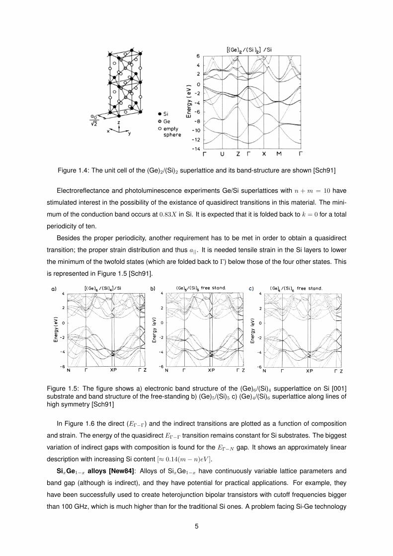
Figure 1.4: The unit cell of the (Ge)2/(Si)2 superlattice and its band-structure are shown [Sch91]
Electroreflectance and photoluminescence experiments Ge/Si superlattices with n + m = 10 have
stimulated interest in the possibility of the existance of quasidirect transitions in this material. The mini-
mum of the conduction band occurs at 0.83X in Si. It is expected that it is folded back to k = 0 for a total
periodicity of ten.
Besides the proper periodicity, another requirement has to be met in order to obtain a quasidirect
transition; the proper strain distribution and thus a||. It is needed tensile strain in the Si layers to lower
the minimum of the twofold states (which are folded back to Γ) below those of the four other states. This
is represented in Figure 1.5 [Sch91].
Figure 1.5: The figure shows a) electronic band structure of the (Ge)6/(Si)4 supperlattice on Si [001]substrate and band structure of the free-standing b) (Ge)5/(Si)5 c) (Ge)4/(Si)6 superlattice along lines ofhigh symmetry [Sch91]
In Figure 1.6 the direct (EΓ−Γ) and the indirect transitions are plotted as a function of composition
and strain. The energy of the quasidirect EΓ−Γ transition remains constant for Si substrates. The biggest
variation of indirect gaps with composition is found for the EΓ−N gap. It shows an approximately linear
description with increasing Si content [≈ 0.14(m− n)eV ].
SixGe1−x alloys [New84]: Alloys of SixGe1−x have continuously variable lattice parameters and
band gap (although is indirect), and they have potential for practical applications. For example, they
have been successfully used to create heterojunction bipolar transistors with cutoff frequencies bigger
than 100 GHz, which is much higher than for the traditional Si ones. A problem facing Si-Ge technology
5

Figure 1.6: Transition energies of various n+m = 10 superlattices s as a function of lateral strain in theSi layer are represented [Sch91]
is the mismatch that causes compressive strain in SixGe1−x layers grown on Si. According to Vegard’s
law, in a SixGe1−x alloy, a|| = xaSi + (1− x)aGe, in which aSi and aGe are the cubic lattice constants of
Si and Ge structures, respectively. The strain increases with increasing Ge concentration and the strain
energy increases with Si-Ge film thickness as well.
The band structure for SixGe1−x alloys was calculated in reference [New84] (Figure 1.7)
Figure 1.7: Band structures E(~k) for the principal symmetry directions of the diamond lattice for (a)Si0.2Ge0.8 and (b) Si0.74Ge0.26 where calculated [New84]
The band gap, Eg, is indirect, with the valence-band maximum in the Γ point and the conduction-
band minimum changes from L [L = (2π/a)( 12 ,
12 ,
12 )] to near the point X [= (2π/a)(1, 0, 0)]. The change
occurs at approximately x = 0.25 (for a temperature of 4K). It is this feature that makes the defect levels
of this alloy interesting to study, since alloys with compositions near the x = 0.25 can possibly produce
deep levels in the gap for impurities such as As and P [New84].
Near the band gap, every sp3 bonded impurity with a valence greater than that of tetrahedrally
bonded host by unity is expected to have an s-like level, a triply degenerate p-like deep level. In Figure
1.8 [New84] is shown the predicted single-impurity defect levels of p-like and s-like symmetries. Shown
are also in these figures the conduction-band minima as functions of composition x where the zero of
energy is taken to be the to of the valence band maxima for all x.
6

Figure 1.8: The figures show the predicted single-impurity defect levels of a) T2 and b) A1 symmetry asa function of the composition x. Shown are also the conduction and valence band edges [New84]
Magic sequence SiGe2Si2Ge2Si and the genetic algorithm [d’A12]: Using a genetic algorithm it
was identified the sequence of Si and Ge layers with strong transition across the electronic band-gap
from amongst all possible superlattices [Sin0Gep0 /Sin1
Gep1 /.../SinNGepN ]∞ including substrate orienta-
tion and strain.
It is used a efficient optimization method: A population of superlattices is “genetically” selected ac-
cording to chance and their relative success, namely, their ability for light-emission at the band-edges.
New superlattice candidates (offspring) are created from the previous population by interchanging ran-
dom sets of layers in the superlattice between two parents (crossover), and by flipping random Ge layers
into Si layers and vice-versa in a single parent (mutation). At each generation, the worst individuals in
the previous population are replaced by the best offspring, thus guiding the population as a whole to-
wards the global optimum through survival of the fittest. To judge fitness, i.e., the strength of the optical
transition, it is computed the dipole matrix element between the valence band minimum and conduction
band maximum at Γ of each superlattice candidate, which is directly proportional to the strength of the
optical transition.
The set of results are a variation of a magic sequence composed of α =SiGe2Si2Ge2Si followed
by a Germanium buffer layer of n = 12 − 32 monolayers. The magic sequence satisfies: wave vector
directness and the dipole matrix element between the valence band maximum and the conduction band
minimum is nonzero. The first condition is satisfied when the structure is grown on substrates Si1−xGex
with x ≥ 0.4 (Figure 1.9).
The second condition is shown by the spectrum of absorption in Figure 1.10 top, which also contains
the spectrum of absorption for the superlattice Si6Ge4 compared with the “magical” sequence.
They evaluated the effect of deviation of the best sequences in the “directness” of the band gap. By
changing the substrate and the mutations in the magic sequence, it was constructed Figure 1.11. αn is
the magic sequence with a Ge buffer of n monolayers, while β is the sequence SiGe2Si2Ge2SiGe2SiGe9
and γ the sequence SiGe2SiGe2Si2Ge2SiGe2SiGe6.
7

Figure 1.9: Band structures of the α12 magic sequence grown on Si0.4Ge0.6 where calculated [d’A12]
Figure 1.10: The figure shows the comparison between Si6Ge4 superlattice and the magic sequence ofthe direct absorption spectra [d’A12]
Figure 1.11: Direct dipole-allowed band-gaps as calculated by [d’A12]
Si and Ge heterostructures with C impurities
A possible solution to the mismatch problem is the incorporation of C which has a lattice constant of
3.57A in a Diamond crystal structure, which is much smaller than those of Si and Ge. Incorporation of C
into SiGe material should reduce the lattice mismatch because of the smaller size of C, compensating
for the larger size of Ge. The linear approximation for the lattice constant between Si, Ge, and diamond
is [Ost98]
8

a(x, y) = (1− x− y)aSi + xaGe + yaC , (1.3)
resulting in a Ge:C ratio of 8.2 for strain compensation. The incorporation of a third component also adds
additional flexibility in band-gap engineering. This could pose a challenge to the GaAs technologies. We
define an “effective lattice-mismatch” mfeff as [Ost98]
mfeff =a(x, y)− aSi
aSi, (1.4)
for ternary Si1−x−yGexCy on Si(001) substrates. A positive mfeff that the material is compressively,
mfeff < 0 is tensile strain, and mfeff = 0 means strain-compensated Si1−x−yGexCy alloy. The hydro-
static contribution is [Ost98]
∆Eh = av,c(ε⊥ + 2ε||), (1.5)
where av,c is the appropriate hydrostatic deformation potential for the valence or conduction band, re-
spectively. For the material dependent term ∆Ea,
∆Ea(x, y) = ∆Ea(x) + ∆Ea(y), (1.6)
Figures 1.12, 1.13 and 1.14 summarize the results for the offsets of strained Si1−x−yGexCy on Si(001)
[Ost98]. The effective concentration corresponds to the concentration needed for identically strained
binary layers.
Figure 1.12: Valence-band offsets for compressive strained Si1−xGex , and Si1−x−yGexCy (x =10%,20%, and 30%) and tensile strained Si1yCy and Si1−x−yGexCy (y =1%, 2%, and 3%) are plotted as afunction of the effective lattice mismatch (expressed in “effective” Ge or C concentrations, respectively)[Ost98]
The band-gap narrowing is obtained by adding the valence and the conduction-band offsets. The
band gap for the alloys is always smaller than that of silicon. The addition of C (Ge) into compressive
strained Si1−xGex (tensile strained Si1−yCy) leads to a smaller change in band-gap narrowing than in
an equivalent strain reduction in the binary alloy (lower Ge or C content, respectively).
9

Figure 1.13: Conduction-band offsets for compressive strained Si1−xGex , and Si1−x−yGexCy (x =10%,20%, and 30%) and tensile strained Si1yCy and Si1−x−yGexCy (y =1%, 2%, and 3%) are plotted as afunction of the effective lattice mismatch (expressed in “effective” Ge or C concentrations, respectively)[Ost98]
Figure 1.14: The band-gap narrowing for ternary Si1−x−yGexCy alloys, strained on Si(001) is repre-sented as a function of lattice mismatch as calculated by [Ost98]
10

1.3 Thesis Outline
This thesis is organized as follows:
In chapter 2 we will make a theoretical introduction with the physics needed to this project. Starting
by the by the many body problem, going through the Density Functional Theory (DFT) justify the use of
an independent electron approximation for the problem. We use pseudopotentials, so we explain what
is a pseudopotential, using not only local pseudopotentials but also the non-local (important in Carbon)
and spin-orbit contributions (important in the heavier Germanium) that are needed to fully describe bulk
group IV elements in question.
In chapter 3 we describe the search for the best pseudopotentials fitted to the experiment. We start
from a previous description used for Silicon with only a local pseudopotential. After we improve the
description by adding a non-local contribution to the pseudopotential. We search for the best fitted local
and non-local parts of the pseudopotential to the experiment and calculate the optical properties. The
same search is done for Carbon. For Germanium we add a spin-orbit contribution and find as well the
best fitted potentials (local, non-local and spin-orbit) to the experimental results.
The software used is MATHEMATICA. It is good for the development and learning process, but has
limitations such as the computation time increases highly with the precision requested for the calculation.
In chapter 4 the pseudopotentials developed here are used in a FORTRAN program, where numerically
converged and obtained in a resonable amount of time, in particular for large simulation cells. An
indication of future research was also made.
11
Chapter 2
Theoretical Introduction
We want to calculate the properties of a solid - a condensed matter system. This task can be quite
complicated, if not impossible to solve. Most of the time we have to use approximations to calculate the
properties of the system, which means we have always to keep in mind those approximations and what
they change in the final result. We start from the beginning of the problem: the many body problem,
because that is what we have, a solid with a big number of electrons and nucleus. Afterwards we are
going to describe the independent electron approximation with the use of pseudopotentials which is
reasonable to describe solids. What is here written, from section 2.1 to 2.7, is based on the notes of
reference [Mar].
2.1 The many-body problem
Consider a system of m electrons and n nuclei, each one with spatial coordinates ~ri and ~Rj and spin
ξi and Ξj . In the non-relativistic limit, the time-independent Schrodinger equation that can be used to
calculate the properties of the system is
HΦ(~r1, ξ1, . . . , ~rm, ξm, ~R1,Ξ1, . . . , ~Rn,Ξn) = EΦ(~r1, ξ1, . . . , ~rm, ξm, ~R1,Ξ1, . . . , ~Rn,Ξn), (2.1)
where the many particle Hamiltonian is
H =
n∑i=1
− 1
2Mi∇2~Ri
+
m∑j=1
−1
2∇2~rj
+∑i<j
ZiZj
|~Ri − ~Rj |+∑i<j
1
|~ri − ~rj |−∑i,j
Zi
|~Ri − ~rj |. (2.2)
The subscripts in the Laplacian ∇2 indicate on which coordinate they operate. Mi and Zi are the
mass and the charge, respectively, of the ith nucleus. The terms in the Hamiltonian are, respectively,
the kinetic energy of the nuclei and the electrons, the potential energy related to the potential caused by
the nuclei and felt by the nuclei, the potential caused by the electrons and felt by them and the potential
caused by the ions and felt by the electrons (or vice versa). Notice that it is written in an adimentional
form, adequate to computational purposes. These units are called atomic units, a system in which the
12

numerical values of following fundamental physical constants are all unity by definition: the electron
mass, me, the elementary charge, e, the reduced Planck’s constant ~ = h2π and the Coulomb’s constant
14πε0
, where ε0 is the dielectric permittivity of vacuum. In this work, all the equations will be written in the
atomic system of units unless it is said otherwise.
Since electrons are fermions, the wavefunction is anti-symmetric with respect to the electron coordi-
nates, position and spin (Pauli’s exclusion principle),
Φ(. . . , ~ri, ξi, . . . , ~rj , ξj , . . .) = −Φ(. . . , ~rj , ξj , . . . , ~ri, ξi, . . .). (2.3)
An analytical solution for the equation (2.1) with the Hamiltonian (2.2) is only known for very simple
systems such as the Hydrogen atom and the H+2 ion, and numerical solutions can be obtained for atoms
and molecules with a small number of electrons such as the He atom or the H2 molecule. These are
very simple systems. No such miracle is to be expected for larger systems. If we could solve the exact
Hamiltonian for these more complicated systems we could in principle predict all of it’s properties. In a
macroscopic solid, there are about 1023 nuclei and a similar number of electrons [All10]. The equation
(2.1) to be solved would have something in the order of 1023 variables, which is not possible with the
current computational technology.
Therefore we are compelled to make approximations motivated by physical considerations, such as
those described in the following sections.
2.2 The Adiabatic Approximation
The first approximation to be made takes into account that the mass of the nuclei is much larger (gen-
erally 104 − 105 times [All10]) than the mass of the electrons, Mi me. Therefore we can say that
the nuclear motion is much slower (or say the nuclei are fixed) than the motion of the electrons. In this
way we can neglect their Kinetic Energy, obtaining the Hamiltonian He for the electronic problem, which
depends on the nuclear coordinates,
He =
m∑j=1
−1
2∇2~rj
+∑i<j
ZiZj
|~Ri − ~Rj |+∑i<j
1
|~ri − ~rj |−∑i,j
Zi
|~Ri − ~rj |HeΨ
(k)(~r1, . . . , ~rm; ~R1, . . . , ~Rn) = U (k)(~R1, . . . , ~Rn)Ψ(k)(~r1, . . . , ~rm; ~R1, . . . , ~Rn), (2.4)
and whose eigenvalues also depend on the position and spin of the nuclei and form a family identified
by the quantum number (k). This is called the Born-Oppenheimer or adiabatic approximation [BH88].
The energy U (k) can be considered as the potential energy in the Hamiltonian used in the Schrodinger
equation that describes the motion of the nuclei
H(k)N =
n∑i=1
− 1
2Mi∇2~Ri
+ U (k)(~R1, . . . , ~Rn)
13

H(k)N χ(k,q)(~R1, . . . , ~Rn) = E(k,q)χ(k,q)(~R1, . . . , ~Rn), (2.5)
where the quantum number q concerns the vibrational, rotational and translational states. We say that
the total wave function is the product of the solutions of the equations (2.4) and (2.5),
Θ(k,q)(~r1, . . . , ~rm; ~R1, . . . , ~Rn) ' Ψ(k)(~r1, . . . , ~rm; ~R1, . . . , ~Rn)χ(k,q)(~R1, . . . , ~Rn), (2.6)
which is a complete set expansion of the wavefunction Φ =∑k,q ck,qΨ
(k)χ(k,q). The decoupling of the
electronic and nuclear motions can also be obtained using perturbation theory.
2.3 Separable Schrodinger equation
But the problems in the equation (2.2) are almost the same as the ones in equation (2.4) since we still
have a number of electrons in the order of 1023 which interact with one another through this Coulomb
interaction and thus we cannot separate the Schrodinger equation in its different variables. We could
neglect the Coulomb interaction but unfortunately we know this is a bad approximation. Another solution
is to consider that a given electron is subjected by a potential depending on the average distribution of
the electrons. This results in the Hamiltonian [All10]
Hs =
m∑j=1
−1
2∇2~rj
+
m∑j=1
n∑i=1
Vat(~rj − ~Ri)
=
m∑j=1
[−1
2∇2~rj
+
n∑i=1
Vat(~rj − ~Ri)
]=
m∑j=1
Hj , (2.7)
where Vat includes the average Coulomb electron-electron and the electron-nucleus interaction. The
nucleus-nucleus term is dropped, since it is a constant for the same position of the nuclei. Doing this, it
is possible to separate the Hamiltonian into a sum of m independent terms, each acting on a different
coordinate.
2.4 The Hartree-Fock Method
We can construct and anti-symmetric wave-function using a Slater determinant of orthonormal one
electron spin orbitals, φi(~r), i = 1, ...,m,
D(~r1, . . . , ~rm) =1√m!
∣∣∣∣∣∣∣∣∣∣∣∣
φ1(~r1) φ1(~r2) . . . φ1(~rm)
φ2(~r1) φ2(~r2) . . . φ2(~rm)...
.... . .
...
φm(~r1) φm(~r2) . . . φm(~rm)
∣∣∣∣∣∣∣∣∣∣∣∣, (2.8)
in which 〈φi| φj〉 = δij . In this case we can show that 〈D| D〉 = 1.
We use the variational principle in quantum mechanics to calculate de ground state energy E0 and
14

wavefunction Ψ0 of the many-body system,
E0 = min〈Ψ | H | Ψ〉〈Ψ | Ψ〉
, E0 =〈Ψ0 | H | Ψ0〉〈Ψ0 | Ψ0〉
. (2.9)
In the Hartree-Fock method we search the wavefuntions in the form of Slater determinants,
EHF = min〈D | H | D〉, EHF = 〈DHF | H | DHF 〉, (2.10)
where we always have that EHF ≥ E0. To minimize the energy in equation (2.10) the Euler-Lagrange
method can be used,
δ
δφ∗j
[〈D | H | D〉 −
∑ij
λij(〈φi | φj〉 − δij
)]= 0, (2.11)
where λij are the Lagrange multipliers. The expectation value of the energy for the Slater determinant
is
〈D | H | D〉 =∑i
∫φ∗i (~r)
(−1
2∇2)φi(~r)d
3r
+∑i
∫φ∗i (~r)
(∑j
−Zj|~r − ~Rj |
)φi(~r)d
3r
+∑i<j
ZiZj
|~Ri − ~Rj |
+1
2
∑i,j
∫∫φ∗i (~r)φ
∗j (~r′)
1
|~r − ~r′|φi(~r)φj(~r
′)d3rd3r′
− 1
2
∑i,j
∫∫φ∗i (~r)φ
∗j (~r′)
1
|~r − ~r′|φi(~r
′)φj(~r)d3rd3r′, (2.12)
that is a sum of five contributions: kinetic, external potential, ion-ion, Hartree and exchange. The ion-ion
contribution is a constant. We can define the external ionic potential,
v(~r) =∑j
−Zj|~r − ~Rj |
, (2.13)
and the total electronic charge density,
ρ(~r) = 〈D |∑i
δ(~ri − ~r) | D〉 =∑j
φ∗j (~r)φj(~r). (2.14)
With this definitions we can rewrite the external potential and the Hartree contributions,
∫v(~r)ρ(~r)d3r,
1
2
∫∫ρ(~r)ρ(~r′)
|~r − ~r′|d3rd3r′. (2.15)
Introducing (2.15) into (2.12) and the later in (2.11) we obtain the Hartree-Fock equations,
15

[−1
2∇2 + v(~r) +
∫ρ(~r′)
|~r − ~r′|d3r′
]φi(~r)−
∑j
φj(~r)
∫φ∗j (~r
′)1
|~r − ~r′|φi(~r
′)d3r′ =∑j
λijφj(~r). (2.16)
Knowing that the Slater determinants are invariant with respect to unitarian transformations Ψi →
Ψ′j =∑i UijΨi, we can use this do diagonalize (2.16), obtaining
[−1
2∇2 + v(~r) +
∫ρ(~r′)
|~r − ~r′|d3r′
]φi(~r)−
∑j
φj(~r)
∫φ∗j (~r
′)1
|~r − ~r′|φi(~r
′)d3r′ = εiφi(~r). (2.17)
The correlation energy Ec = E0 − EHF is the difference between the exact energy of a system
and the Hartree-Fock energy. This equation is a non-linear eigenvalue differential integral equation
in 3 dimensional space. The Hartree-Fock method provides a connection between the many body
wavefuntion to m one body wavefunctions.
2.5 Density Functional Theory
Density functional theory is a method to investigate the electronic structure in the ground state of atoms,
molecules or condensed matter systems. It says that the properties of a many-electron system can
be uniquely determined by the ground state electron density of the system, that depends on 3 spatial
coordinates.
But before we have to make sure that the properties of the system can be indeed be uniquely asso-
ciated to a determined electron density (ilustration in the Venn Diagram in Figure 2.1).
Figure 2.1: The figure shows the Venn’s diagram corresponding a potential in the space of all potentialsV (~r) to a ground state electron density in the space of the ground state electron densities ρGS(~r)
If it is univocal, in principle, by knowing the electron density, we can obtain the potential that acts on
this electrons and from that we can calculate the ground state eigenfunctions and all the other properties
of the system.
16

First let us assume that two different potentials can lead to the same ground state electron density,
V1(~r) - Ψ1(~r) XXXXXz
V2(~r) - Ψ2(~r) : ρGS(~r),
and consider the Hamiltonian
H = T + Vee + Vext, (2.18)
where,
T =∑i−
12∇
2~ri
Vee =∑i<j
1|~ri−~rj |
Vext =∑i v(~ri), (2.19)
are the Kinetic, Coulomb Potential and external Potential energies, respectively and v(~ri) is given by
equation (2.13). We calculate de ground state energy using V1,
EGS1 = 〈Ψ1|T + Vee + V1 |Ψ1〉
= 〈Ψ1|T + Vee |Ψ1〉+
∫V1(~r)ρGS(~r)d3r. (2.20)
Using the variational principle,
〈Ψ2|T + Vee + V1 |Ψ2〉 = 〈Ψ2|T + Vee |Ψ2〉+
∫V1(~r)ρGS(~r)d3r
= 〈Ψ2|T + Vee |Ψ2〉+
∫V2(~r)ρGS(~r)d3r +
∫(V1 − V2)(~r)ρGS(~r)d3r
= EGS2 +
∫(V1 − V2)(~r)ρGS(~r)d3r, (2.21)
so,
EGS1 < EGS2 +
∫(V1 − V2)(~r)ρGS(~r)d3r. (2.22)
But starting with the calculation of EGS2 and following the same line of thinking we get
EGS2 < EGS1 +
∫(V2 − V1)(~r)ρGS(~r)d3r, (2.23)
which results with,
EGS1 > EGS2 +
∫(V1 − V2)(~r)ρGS(~r)d3r
EGS1 < EGS2 +
∫(V1 − V2)(~r)ρGS(~r)d3r, (2.24)
17

that is a contradiction. We reach then the conclusion that in the absence of degeneracies, two different
potentials cannot lead to the same electron density in the ground state. This means that any property of
the many-body system is a functional of ρ(~r). From that comes the name Density Functional Theory.
2.6 Hohenberg-Kohn Theorem
Considering a system of m electrons, the electronic Hamiltonian can be described by Equation (2.18),
we define the set of all normalized anti-symmetric wavefunctions as
A = Ψ | Ψ(. . . , ~ri, . . . , ~rj , . . .) = −Ψ(. . . , ~rj , . . . , ~ri, . . .) and 〈Ψ | Ψ〉 = 1. (2.25)
We can define the ground state energy of the system as a functional of the external potential Vext(~r)
as
E[Vext] = minΨ∈A〈Ψ | H | Ψ〉. (2.26)
The subset Aρ of A is the set of all wavefunctions that correspond to the charge density ρ(~r),
Aρ = Ψ | Ψ ∈ A and m
∫d3r2 . . .
∫d3rm|Ψ(~r, ~r2, . . . , ~rm)|2 = ρ(~r). (2.27)
An universal functional of the charge density is [Lie83]
F [ρ] = minΨ∈Aρ
〈Ψ | T + Vee | Ψ〉, (2.28)
which is independent of Vext(~r). The ground state energy can be calculated as a functional of the
electron density ρ for each potential Vext,
E0 = EGS [ρ] = minΨ∈A〈Ψ|T + Vee + Vext |Ψ〉
= minρ
minΨ∈Aρ
〈Ψ|T + Vee + Vext |Ψ〉
= minρ
[min
Ψ∈Aρ(〈Ψ|T + Vee |Ψ〉+ 〈Ψ|Vext |Ψ〉)
], (2.29)
in which 〈Ψ|Vext |Ψ〉 =∫Vext(~r)ρ(~r)d3r, so
EGS [ρ] = minρ
[∫Vext(~r)ρ(~r)d3r + min
Ψ∈Aρ〈Ψ|T + Vee |Ψ〉
]= min
ρ
[F [ρ] +
∫Vext(~r)ρ(~r)d3r
]= min
ρEVext [ρ]. (2.30)
Therefore Hohenberg-Kohn theorem states that the minimum of the energy functional EVext is the
ground state energy E0 of the system. Note that contrary to the previous proof, we did not require the
ground state of the system to be non-degenerate.
18

2.7 Kohn-Sham Equations
Consider the set of one electron wavefunctions φi and occupation numbers fi that have a charge density
equal to ρ ,
Bρ = (f1, . . . , fk, φ1, . . . , φk) | 〈φi | φj〉 = δij ,
k∑i=1
fi|φi(~r)|2 = ρ(~r) fi ∈ [0, 1], (2.31)
where some authors define 0 ≤ fi ≤ 1, and we define an energy functional of the charge density ρ that
it is called kinetic energy functional but it is not the true kinetic energy of the system
T0[ρ] = min(f1,...,fk,φ1,...,φk)∈Bρ
k∑i=1
fi〈φi | −1
2∇2 | φi〉. (2.32)
The exchange and correlation functional energy is defined as
Exc[ρ] = F [ρ]− 1
2
∫∫ρ(~r)ρ(~r′)
|~r − ~r′|d3rd3r′ − T0[ρ], (2.33)
where F [ρ] was defined in equation (2.28). It contains the rest of the many-body contributions to the
energy. Also since T0[ρ] is not the exact kinetic energy of the interacting energy but instead the kinetic
energy of the ground state of a system of non interacting electrons with density ρ(~r), Exc[ρ] contains
also kinetic energy terms. Rewriting it in a different way, we have
F [ρ] = T0[ρ] +1
2
∫∫ρ(~r)ρ(~r′)
|~r − ~r′|d3rd3r′ + Exc[ρ]. (2.34)
We can calculate the energy functional,
EVext [ρ] = F [ρ] +
∫Vext(~r)ρ(~r)d3r
= T0[ρ] +
∫Vext(~r)ρ(~r)d3r +
1
2
∫∫ρ(~r)ρ(~r′)
|~r − ~r′|d3rd3r′ + Exc[ρ], (2.35)
and the ground state energy,
EGS [ρ] = minρEVext [ρ]
= minρ
(T0[ρ] +
∫ρ(~r)Vext(~r)d
3r +1
2
∫∫ρ(~r)ρ(~r′)
|~r − ~r′|d3rd3r′ + Exc[ρ]
)= min
ρ
(min
(f1,...,fk,φ1,...,φk)∈Bρ
k∑i=1
fi〈φi | −1
2∇2 | φi〉+
∫ρ(~r)Vext(~r)d
3r+
+1
2
∫∫ρ(~r)ρ(~r′)
|~r − ~r′|d3rd3r′ + Exc[ρ]
)= min
ρmin
(f1,...,fk,φ1,...,φk)∈Bρ
( k∑i=1
fi〈φi | −1
2∇2 | φi〉+
∫ρ(~r)Vext(~r)d
3r+
+1
2
∫∫ρ(~r)ρ(~r′)
|~r − ~r′|d3rd3r′ + Exc[ρ]
), (2.36)
19

but this is the same as minimizing over all wavefunctions and therefore,
EGS [ρ] = min(f1,...,fk,φ1,...,φk)
( k∑i=1
fi〈φi | −1
2∇2 | φi〉+
∫ρ(~r)Vext(~r)d
3r +1
2
∫∫ρ(~r)ρ(~r′)
|~r − ~r′|d3rd3r′ + Exc[ρ]
).
(2.37)
The Euler equation that minimizes the expression above with respect to the one electron wavefunc-
tions φi is
δ
δφ∗i
( k∑i=1
fi〈φi | −1
2∇2 | φi〉+
∫ρ(~r)Vext(~r)d
3r +1
2
∫∫ρ(~r)ρ(~r′)
|~r − ~r′|d3rd3r′
+Exc[ρ]−∑i,j
λi,j(〈φi| φj〉)− δij)
= 0, (2.38)
with Vext given by Equation (2.19), is called the Kohn-Sham equation. The result of the minimization is
−1
2∇2 + v(~r) + vH(~r; ρ] + vxc(~r; ρ]
φi(~r) = εiφi(~r),
vH(~r; ρ] =
∫ρ(~r′)
|~r − ~r′|d3r′,
vxc(~r; ρ] =δExc[ρ]
δρ(~r),
ρ(~r) =
k∑j=1
fjφ∗j (~r)φj(~r), (2.39)
where vH is the Hartree potential and vxc is the exchange and correlation potential. The curve paren-
thesis in (~r; ρ] means that the function is dependent of a variable, and the square parenthesis indicate a
functional dependence. Although the equation resembles the Schrodinger equation for non-interacting
particles, the dependence of vH and vxc in the charge density ρ makes it a non-linear system of equa-
tions. A common approximation is the Local Density Approximation (LDA) that says that the exchange
and correlation energy depends only on the charge density in the point of interest vxc(~r) = vxc[ρ(~r)].
The way to solve this kind of equations is through iterative, self-consistent methods. The kind of logic is
the following:
1. Guess initial ρin
2. Calculate vH [ρin] and vxc[ρin]
3. Solve the Kohn-Sham equation
4. Calculate ρout =∑i |φi(~r)|2
5. If ρin ∼ ρout stop. If not ρin = F (ρin, ρout) and start from 2.
Although it is a highly used method, the DFT with LDA gives the wrong value for the band gap, for
example almost half of the value for the band gap of silicon.
20

2.8 Pseudopotentials
The pseudopotential model describes a periodic solid as a sea of valence electrons moving in a back-
ground of cores. The space can be divided into two regions: the region near the nuclei, the “pseudized
core” composed primarily of tightly bound core electrons which are not very affected by the neighbour
atoms; and the valence electron region which is involved in bonding the atoms together. The pseu-
dopotential only acts on the valence electrons. This results that the atoms in the same group - such as
Carbon, Silicon and Germanium (group IV, for ex.) - are treated in mostly the same way, apart from a
few “details”. The focus of the calculation is only on the accuracy of the valence electron wavefunction
away from the core. The potential in the ion core is strongly attractive for the valence electrons, but the
requirement for the valence wavefuntions to be orthogonal to those of the core contributes to an effec-
tive repulsive potential for valence states. This results in a net weakly attractive potential that affects the
valence electrons.
2.8.1 Ab initio pseudo-potentials
We first consider an atom of atomic number Z. An one-electron Hamiltonian can be written as [CC92]
H =1
2∇2 + Vion + Vscr, (2.40)
where Vion = −Zr is the ion core potential, that can be taken as a linear superposition of spherical
potentials, and Vscr is the screening potential, a potential very important in many body physics. Usually
it is divided into two parts (as it was seen before), the Hartree potential, VH(~r, ρ], that comes from the
Poisson’s equation
∇2VH = −4πe2ρ(~r), (2.41)
where ρ(~r) is the valence electron charge density. The other part is the exchange and correlation
potential Vxc, that was also mentioned before. If we use the Local Density Approximation (LDA), then
Vxc(~r) = Vxc[ρ(~r)]. The total potential is, thus
VT (~r) = Vion(~r) + VH + Vxc(~r). (2.42)
If there is one state for which we know the the wavefuntion and the value of the energy we can invert
the Schrodinger equation to obtain the total potential [CC92]
VT =1
2
∇2Ψ
Ψ+ E. (2.43)
This equation is well behaved if Ψ is nodeless, since it is highly preferable for the pseudopotential to
be smooth and the wiggles associated with the nodes are undesirable. The quantity ∇2ΨΨ is extremely
sensitive to numerical errors when Ψ → 0. If there are no numerical errors, what normally happens is
that if Ψ → 0, then ∇2Ψ → 0 as well. If there is an error and ∇2Ψ doesn’t go to zero when Ψ → 0, this
21

quantity will diverge.
In an atom, we can extract the energy levels of interest by performing an atomic structure calculation
starting from all electron atomic calculations. Within the density-functional theory this is done by assum-
ing a spherical screening approximation and self-consistently solving the radial Kohn-Sham equation
[TM91]
[−1
2
d2
dr2+l(l + 1)
2r2+ VT (~r, ρ]
]rRnl(r) = εnlrRnl(n), (2.44)
that results in the “all electron” wavefuntions and energies. We have to take into account that we are
going to perform an inversion of the Schrodinger equation, which is only well behaved if the wavefuntions
used have no nodes (see eq. (2.43)). This can be achieved by the construction of pseudo-wave functions
with no nodes (for this reason, the quantum number n will be omitted in the further calculations) based
on the wavefunctions of the equation (2.44) as it was done successfully in reference [TM91]. Other char-
acteristics of this pseudo-wave funtion are [TM91]: the normalized atomic radial pseudo-wave-function
with angular momentum l is equal to the normalized radial all-electron wave function after a cutoff radius
rcl,
RPPl (r) = RAEl (r) for r > rcl; (2.45)
the charge enclosed for the two wavefuntions within rcl must be equal,
∫ rcl
0
|RPPl (r)|2r2dr =
∫ rcl
0
|RAEl (r)|2r2dr, (2.46)
so that the norm of the wavefunction is conserved after normalization; and the valence all-electron and
pseudopotential eigenvalues must be equal,
εPPl = εAEl . (2.47)
A pseudopotential under this conditions is called a “norm-conserving pseudopotential”. Once we
have the pseudo-wave function we can calculate the pseudopotential by inversion of the Schrodinger
equation [TM91],
V PPl = εl −l(l + 1)
2r2+
1
2rRPPl (r)
d2
dr2[rRPPl (r)]. (2.48)
By inverting the Schrodinger equation for each of the wavefunctions separately, we get with differ-
ent potentials for each quantum number l, Vl. This is called non-locality of the pseudopotential. The
pseudopotential is decomposed into a sum over angular momentum components [CC92],
VT = V0P0 + V1P1 + V2P2 + ..., (2.49)
where the P` projects out the `th angular momentum component,
22

P` = |`m〉 〈`m| , (2.50)
where 〈~r| `m〉 = Y ∗`m(Ω) and Y ∗`m(Ω) is centered on the origin. Another complication is to take into
account the spin orbit effects in heavier elements (like Ge). Non-locality and spin-orbit considerations
will be further developed in later sections.
2.8.2 Empirical Pseudopotential methods
The empirical pseudopotential method relies on experimental results for the construction of the pseu-
dopotential and the predictions made with the pseudopotentials should converge as best as possible
with experience.
Lets assume first that the pseudopotential is local, i.e., independent of `. The Schrodinger equation
for a periodic system is [Che96]
(−1
2∇2 + V (~r)
)ψ~k(~r) = E(~k)ψ~k(~r). (2.51)
In a crystal, the potential V (~r) is periodic in the lattice. We can use a plane wave expansion that
will only have plane waves with the periodicity of the lattice. With the local approximation, the general
approximation for the pseudopotential is
V (~r) =∑~G
V (~G)S(~G)ei~G·~r =
∑~G
U(~G)ei~G·~r, (2.52)
where ~G is a reciprocal lattice vector, V (~G) are the form factors and S(~G) is the structure factor,
S(~G) =1
Na
Na∑i=1
ei~G·~τi . (2.53)
Once the form factors are chosen, we can solve (2.51). We can assume that the wave functions
ψ~k(~r) can be expanded in plane waves, with no loss of generality and solve the secular equation, which
is the Schrodinger equation (2.51) in the reciprocal space [Che96, AM76],
det |H(~k, ~G− ~G′)− E(~k)I| = 0, (2.54)
where
H(~k, ~G− ~G′) =1
2(~k − ~G)2δ~G,~G′ + V (~G− ~G′)S(~G− ~G′). (2.55)
The form factors depend only on the magnitude of |~G − ~G′| if the pseudopotential can be taken
as spherically symmetric, which is generally the case for tetrahedral semiconductors [Che96], with~G discrete. In the Chelikowsky pseudopotential [Che96], for diamond or zinc-blende semiconduc-
tors, generally only three form factors are enough to determine the pseudopotential, those for G2 =
3(
2πa
)2, 8(
2πa
)2, 11
(2πa
)2. The factor G2 = 0 is not important since it only gives the level zero of en-
23

ergy and S(~G) = 0 for G2 = 4(
2πa
)2, 12
(2πa
)2. So of the six smallest reciprocal lattice vectors lengths,
only the form factors G2 = 3(
2πa
)2, 8(
2πa
)2, 11
(2πa
)2 are required to specify the crystalline potential
[CC92][Che96] (Figure 2.2). These three values are fitted to optical transition energies and the whole
band structure follows from them. The method is similar with the one discussed to DFT:
Figure 2.2: The figure shows a schematic plot of a pseudopotential in reciprocal space with the G’s thatcorrespond to G2 = 3, 8, 11 with G2 in units of (2π/a)2[CC92]
1. Estimate initial V (~G)
2. Solve secular equation
3. Calculate band structure and optical properties
4. Compare with experiment
5. If it agrees with experiment stop. If not change V (~G) and start from 2.
In reference [WZ95], a semi-empirical pseudopotential is used. First an ab initio method is used, in
which spherical atomic potentials (with only the local part) vα(r), such that the solutions of
−1
2∇2 + Vnonlocal(~r) +
∑α
∑Rα
v(α)(|~r − ~Rα|)
ψi = εiψi, (2.56)
where α is the chemical atomic type and ~Rα stands for all possible atomic positions of α, including those
related by lattice translations, will have large overlaps with the LDA solutions ψi and εi, so that they
reproduce the LDA results for bulk systems with a good approximation. This means that it will suffer
from poor reproduction of the observed optical energies. Those authors chose a potential described in
the reciprocal space by
v(α)(q) =∑i
Cα(n)e−(q−an)2/b2n , (2.57)
where C(n), an and bn are free parameters (the author used 20 of each), to be adjusted, this time
empirically, to reproduce the experimentally observed excitation energies. Notice the big number of
parameters used in the fit.
24

This work is based in the Empirical Pseudopotential Method. The parameters that are adjusted to
the experiment are not the form factors like in [Che96] but the parameters of a function we define as
the pseudopotential. Also, as this work is predicted to be used in superlattices, we calculate the form
factors for the pseudopotential in a lattice of equally distant points in the reciprocal space. If we want to
describe a superlattice, we need to fit the whole curve of the potential, because in a supperlattice, the~G vectors may not be constant. Like in the work of reference [WZ95], we will be adjusting an empirical
expression to experimental results, but the number of parameters used will be much less and each one
will have a physical meaning.
2.8.3 Non-local and Spin-Orbit Pseudopotentials
If we take into account the spin-orbit effects, we can obtain pseudo-wave-functionsRPP` j (r), with energies
ε` j and normalization∫∞
0r2|RPP
` j (r)|2dr = 1 that are constructed from the respective all-electron wave-
functions. From the inversion of the radial Schrodinger equation we obtain the correspondent ionic
pseudopotentials V PP` j . The index j takes the values ` ± 1
2 , except for ` = 0, where the only allowed
value is j = 12 . It is in this distinct pseudopotentials for j = `− 1
2 and j = `+ 12 that the effect of the spin-
orbit is included in the calculations, as the major spin-orbit effect is in the core region, since the dominant
contribution comes from the motion of electrons in the Coloumb potential in the innermost region of the
atomic cores. To restrict the non-local part of the pseudopotential to the core region we define a local
potential V L(r) that is arbitrary in the core region, and is identical to the pseudopotentials V PP` j (r) outside
the core region (V L = V PP`j for r > rc). We define the non local part of the pseudopotential as
∆V NL` j (~r, ~r′) = V PP
` j (~r, ~r′)− V L(~r). (2.58)
The non-local part of the pseudopotential for ` > `max can be neglected as long as the local part and
`max is reasonably chosen.
It is convenient also to separate the pure spin-orbit part from the average non-local pseudopotential,
because the spin-orbit can often be treated as a small perturbation, which is often not the case of the
non-local component. We therefore define for ` > 0 the degeneracy weighted average
∆V NL` (~r, ~r′) =
`
2`+ 1∆V NL
` `− 12(~r, ~r′) +
`+ 1
2`+ 1∆V NL
` `+ 12(~r, ~r′), (2.59)
and the spin-orbit part
∆V SO` j (~r, ~r′) = ∆V NL
` j (~r, ~r′)−∆V NL` (~r, ~r′). (2.60)
In its semi-local form the action of the pseudopotential operator on a spinor is, in a compact notation
V PP = V L +∑`
∑m
|`m〉V NL` 〈`m|+
∑`
∑j
∑mj
|` j mj〉V SO` j 〈` j mj |, (2.61)
where |`m〉 and |` j mj〉 are angular momentum states, the first with just orbital components the second
25
with the composition of the orbital and spin angular momenta. Semi-local means that it is non-local in
the angular but not radial coordinates.
For pratical implementations it is better to have the full explicit expression with all the integrals in
spherical coordinates, the spherical harmonics Y`m(θ, φ) and the explicit form of the Clebsch-Gordon
coefficients for the composition of an angular momentum ` with a spin 12 (explicit derivation in Appendix
A),
V PP
ψ+ 12(r, θ, φ)
ψ− 12(r, θ, φ)
= V L(~r)
ψ+ 12(r, θ, φ)
ψ− 12(r, θ, φ)
+
`max∑`=0
∑m=−`
∆V NL` (~r, ~r′)
Y`m(θ, φ)∫ 2π
0dφ′∫ π
0sin(θ′)dθ′ Y `m(θ′, φ′)ψ+ 1
2(r, θ′, φ′)
Y`m(θ, φ)∫ 2π
0dφ′∫ π
0sin(θ′)dθ′ Y `m(θ′, φ′)ψ− 1
2(r, θ′, φ′)
+
`max∑`=1
∆V SO` `+ 1
2(~r, ~r′)
0
Y`−`(θ, φ)
∫ 2π
0
dφ′∫ π
0
sin(θ′)dθ′ Y `−`(θ′, φ′)ψ− 1
2(r, θ′, φ′)
+
`max∑`=1
∆V SO` `+ 1
2(~r, ~r′)
Y` `(θ, φ)
0
∫ 2π
0
dφ′∫ π
0
sin(θ′)dθ′ Y ` `(θ′, φ′)ψ+ 1
2(r, θ′, φ′)
+
`max∑`=1
`− 12∑
mj=−(`− 12 )
∆V SO` `+ 1
2(~r, ~r′)
√ 2`+1+2mj4`+2 Y`mj− 1
2(θ, φ)√
2`+1−2mj4`+2 Y`mj+ 1
2(θ, φ)
×(√
2`+ 1 + 2mj
4`+ 2
∫ 2π
0
dφ′∫ π
0
sin(θ′)dθ′ Y `mj− 12(θ′, φ′)ψ+ 1
2(r, θ′, φ′)
+
√2`+ 1− 2mj
4`+ 2
∫ 2π
0
dφ′∫ π
0
sin(θ′)dθ′ Y `mj+ 12(θ′, φ′)ψ− 1
2(r, θ′, φ′)
)
+
`max∑`=1
`− 12∑
mj=−(`− 12 )
∆V SO` `− 1
2(~r, ~r′)
√ 2`+1−2mj4`+2 Y`mj− 1
2(θ, φ)√
2`+1+2mj4`+2 Y`mj+ 1
2(θ, φ)
×(√
2`+ 1− 2mj
4`+ 2
∫ 2π
0
dφ′∫ π
0
sin(θ′)dθ′ Y `mj− 12(θ′, φ′)ψ+ 1
2(r, θ′, φ′)
+
√2`+ 1 + 2mj
4`+ 2
∫ 2π
0
dφ′∫ π
0
sin(θ′)dθ′ Y `mj+ 12(θ′, φ′)ψ− 1
2(r, θ′, φ′)
). (2.62)
From the computational point of view, the semi-local form of the pseudopotential is less efficient
than the full non local form. The procedure of Kleinman and Bylander allows the construction of a fully
non-local potential [TM91, TH01, KB82],
VKB =∑`,m
∣∣∣∆V NL` ΦPP`,m
⟩⟨ΦPP`,m∆V NL
`
∣∣∣⟨ΦPP`,m
∣∣∣∆V NL`
∣∣∣ΦPP`,m⟩ , (2.63)
where ΦPP`,j,mj (r, θ, φ) = RPP`j (r)Y`m(θ, φ).
In the absence of spin terms, we first define a function, referred to as “projector” in the literature
(more details in Appendix B). We write it between quotes because it is not a true projector. One of the
reasons for that is that 〈a`m| a`m〉 6= 1. The function associated with the “projector” is
26

a`m(r, θ, φ) =1√|b`|
∆V NL` (~r, ~r′)R`(r)Y`m(θ, φ), (2.64)
where
b` =
∫ ∞0
r2drR`(r)∆VNL` (~r, ~r′)R`(r), (2.65)
and the non-local KB pseudopotential operator is
V KBψ(r, θ, φ) =
`max∑`=0
∑m=−`
a`m(r, θ, φ)sgn(b`)
∫ ∞0
r′2dr′∫ 2π
0
dφ′∫ π
0
sin(θ′)dθ′ a∗`m(r′, θ′, φ′)ψ(r′, θ′, φ′),
(2.66)
or in shorter notation
V KB =
`max∑`=0
∑m=−`
|a`m〉sgn(b`)〈a`m|, (2.67)
where sgn(b`) determines if the potential is attractive or repulsive. The sgn(b`) in between the ket and
the bra is another difference from a real projector, as the one in equation (2.50). Considering spin, we
have the “projectors”
a` j mj =
a` j mj + 12(r, θ, φ)
a` j mj − 12(r, θ, φ)
, (2.68)
whose definition again include the relevant Clebsch-Gordon coefficients. Notice that the a` j mj are the
spinors and a` j mj ms the components of the spin. For the case mj = ±(`+ 12 ) we have
a` `+ 12 `+
12(r, θ, φ) =
1√|b` `+ 1
2|∆V NL
` `+ 12(~r, ~r′)R` `+ 1
2(r)
Y` `(θ, φ)
0
a` `+ 1
2 −(`+ 12 )(r, θ, φ) =
1√|b` `+ 1
2|∆V NL
` `+ 12(~r, ~r′)R` `+ 1
2(r)
0
Y`−`(θ, φ)
,
for the other case we have
a` `+ 12 mj
(r, θ, φ) =1√|b` `+ 1
2|∆V NL
` `+ 12(~r, ~r′)R` `+ 1
2(r)
√ 2`+1+2mj4`+2 Y`mj− 1
2(θ, φ)√
2`+1−2mj4`+2 Y`mj+ 1
2(θ, φ)
a` `− 1
2 mj(r, θ, φ) =
1√|b` `− 1
2|∆V NL
` `− 12(~r, ~r′)R` `− 1
2(r)
√ 2`+1−2mj4`+2 Y`mj− 1
2(θ, φ)√
2`+1+2mj4`+2 Y`mj+ 1
2(θ, φ)
. (2.69)
where in the Spherical Harmonics Y`m we wrote m = mj −ms, and
27

b` j =
∫ ∞0
r2drR` j(r)∆VNL` j (~r, ~r′)R` j(r), (2.70)
and the non-local KB pseudopotential operator is
V KB
ψ+ 12(r, θ, φ)
ψ− 12(r, θ, φ)
=
`max∑`=0
`+ 12∑
j=max(`− 12 ,
12 )
j∑mj=−j
a` j mj + 12(r, θ, φ)
a` j mj − 12(r, θ, φ)
sgn(b`)×
∫ ∞0
r2dr
∫ 2π
0
dφ′∫ π
0
sin(θ′)dθ′(a` j mj + 1
2(r, θ, φ)ψ+ 1
2(r, θ, φ) + a` j mj − 1
2(r, θ, φ)ψ− 1
2(r, θ, φ)
), (2.71)
or in shorter notation
V KB =
`max∑`=0
`+ 12∑
j=max(`− 12 ,
12 )
j∑mj=−j
|a` j mj 〉sgn(b`)〈a` j mj |. (2.72)
Notice that in the KB formalism it is not possible to separate exactly the spin-orbit part from the non-
spin non-local part because R`(r) 6= R` j(r), although since they are similar, such a separation should
be a good approximation. In the empirical pseudopotential method, we do not have to worry about that
detail. For the non local part we have
a`m(r, θ, φ) = f`(r)Y`m(θ, φ), (2.73)
and for the spin-orbit part we have for the case mj = ±(`+ 12 )
a` `+ 12 `+
12(r, θ, φ) = f`,`+ 1
2(r)
Y` `(θ, φ)
0
a` `+ 1
2 −(`+ 12 )(r, θ, φ) = f`,`+ 1
2(r)
0
Y`−`(θ, φ)
,
and for the other case
a` `+ 12 mj
(r, θ, φ) = f`,`+ 12(r)
√ 2`+1+2mj4`+2 Y`mj− 1
2(θ, φ)√
2`+1−2mj4`+2 Y`mj+ 1
2(θ, φ)
a` `− 1
2 mj(r, θ, φ) = f`,`− 1
2(r)
√ 2`+1−2mj4`+2 Y`mj− 1
2(θ, φ)√
2`+1+2mj4`+2 Y`mj+ 1
2(θ, φ).
(2.74)
where f`j(r) are empirical functions. From the expression of the KB pseudopotential those functions
must behave as r` for small r. It must also decay very rapidly for r > rc. In the recipe in reference
[TM91], the f`j are zero for r > rc.
The representation in equation (2.72) is different than the one that is normally used. What it is more
28

usual is to work with the operator ~L · ~S to the spin-orbit coupling [Kle80].
2.9 Screening
2.9.1 Definitions of the dielectric function
The dielectric funtion ε(ω,~k) has significant consequences to the physical properties of solids. The
electric displacement is defined.
~D = ε0 ~E + ~P , (2.75)
in S.I. units. In this section S.I. units will always be used. In this equation ~E is the electric field, ~P
the polarization and ε0 the dielectric permittivity in space. In the case of linear optics, the induced
polarization depends linearly on the electric field strength in a manner that can often be described by
the relationship.
~P = ε0χ~E, (2.76)
and thus
~D = ε0 ~E + ε0χ~E = ε0(1 + χ) ~E = εε0 ~E, (2.77)
with ε = 1 + χ being the dielectric constant, also known as relative permittivity. The vector ~D is related
to the external applied charge density ρext in the same way as ~E is related to the total charge density
ρ = ρext + ρind, where ρind is the charge density induced in the system by ρext.
The divergence relation of the electric field [Kit76] is
∇ · ~D = ∇ · εε0 ~E = ρext (2.78)
∇ · ~E =ρ
ε0=ρext + ρind
ε0. (2.79)
The relation between the fourier components of ~D and ~E is
~D(~k) = ε0ε(~k) ~E(~k), (2.80)
then we can rewrite (2.78) and (2.79).
∇ · ~E = ∇ ·∑
~E(~k)ei~k·~r =
∑ ρ(~k)
ε0ei~k·~r (2.81)
∇ · ~D = ∇ ·∑
ε0ε(~k) ~E(~k)ei~k·~r =
∑ρext(~k)ei
~k·~r. (2.82)
29

We divide (2.82) by (2.81). Each equations are satisfied term by term, so
ε(~k) =ρext(~k)
ρ(~k)= 1− ρind(~k)
ρ(~k). (2.83)
The electrostatic potentials ϕ and ϕext defined by ~E = −∇ϕ and ~D = −∇ϕext satisfy
∇2ϕ =ρ
ε0(2.84)
∇2ϕext =ρextε0
, (2.85)
so [Kit76]
ϕext(~k)
ϕ(~k)=ρext(~k)
ρ(~k)= ε(~k), (2.86)
where ϕ(~k) is the total or screened potential from the external potential ϕext(~k)
ϕ(~k) =ϕext(~k)
ε(~k), (2.87)
and we need now to find the expression for ε(~k). In the electron gas, in the limit ~k → 0, ε(ω, 0) describes
the collective excitations of the Fermi sea. In the other limit ω → 0, ε(0,~k) describes the electrostatic
screening of the electron-electron and electron-lattice interactions in crystals [Kit76]
2.9.2 Screening in a metal
In a metal we have an uniform gas of electrons of charge concentration −n0e in a background of positive
charge n0e. The dielectric function for real systems is very complicated. Here we will only derive
and work with an approximation. A derivation from reference [Kit76] will be followed. We consider a
sinusoidal variation of positive charge density in the x direction
ρ+(x) = n0e+ ρext(k) sin(kx), (2.88)
where ρext(k) sin(kx) gives rise to an electrostatic field, the external field applied to the electron gas.
We know the relations between the electric field, the potential and the charge density ~E = −∇ϕ and
∇ · ~E = ρε0
, which gives rise to the Poisson equation ∇2ϕ = − ρε0
. For the positive charge we have
ϕ = ϕext(k) sin(kx), ρ = ρext sin(kx), (2.89)
and using the Poisson equation
− k2ϕext(k) sin(kx) = −ρext(k)
ε0sin(kx)⇔ k2ϕext =
ρext(k)
ε0. (2.90)
The electron gas will be subjected to this external potential ϕext and to the induced electrostatic
30

potential ϕind(k) sin(kx) of the deformation of the electron gas itself. And the electron charge density is
ρ−(x) = −n0e+ ρind(k) sin(kx). (2.91)
The amplitude of the total electrostatic potential ϕ(k) = ϕext(k)+ϕind(k) is related to the total charge
density ρ(k) = ρext(k) + ρind(k) by the Poisson equation
k2ϕext =ρext(k)
ε0. (2.92)
In the Thomas-Fermi approximation is assumed that a local internal chemical potential can be de-
fined as a function of the electron concentration at that point. In a region where there is no electrostatic
contribution
µ = ε0F =~2
2m(3π2n0)
23 , (2.93)
at absolute zero, with εF being the Fermi energy. In a region where there is electrostatic potential ϕ
µ = εF (x)− eϕ(x) ' ~2
2m[3π2n(x)]
23 − eϕ(x) ∼=
~2
2m[3π2n0]
23 . (2.94)
This results in the local value of the Fermi level being
εF (x) = eϕ(x) + ε0F , (2.95)
and by a Taylor series expansion of εF as a function of the electron concentration n we have:
εF (n(x)) = ε0F +dεFdn
∣∣∣n=n0
[n(x)− n0]. (2.96)
Using equations (2.95) and (2.96) together:
dεFdn0
[n(x)− n0] = eϕ(x). (2.97)
From (2.93) we can calculate the derivative dεFdn0
= 23εFn0
and thus:
2
3
εFn0
[n(x)− n0] = eϕ(x) = eϕ(x)⇔ n(x)− n0 =3
2n0eϕ(x)
εF, (2.98)
being n(x)− n0 the induced part of the electron concentration and thus
ρind(k) = −e[n(x)− n0] = −3
2n0e2
εFϕ(k) =
3
2n0e2
εF
ρ(k)
k2ε0. (2.99)
From equation (2.83) we discover that
ε(k) = 1− ρind(k)
ρ(k)= 1 +
k2TF
k2with k2
TF =3
2n0
e2
εF ε0. (2.100)
31

2.10 Optical properties
To calculate the optical properties such as reflectance, we first compute the imaginary part of the
dielectric function in the limit ~k → 0, from which we can get the real part from a Kramers-Kroning
transformation. This transformation relates the real and imaginary part of the generalised susceptibility,
χ = χ1 + iχ2, that is related to the dielectric function by ε = 1 + χ = ε1 + ε2, and therefore
ε1 = 1 + χ1,
ε2 = χ2, (2.101)
where the index 1 denotes the real part and 2 the imaginary part. By using the Kramers-Kroning trans-
formation we get the real part of the susceptibility from the imaginary part [Lan80]
χ1(ω) =2
πP
∫ +∞
0
ξχ2(ξ)
ξ2 − ω2dξ, (2.102)
where P denotes the principal part of the integral. The real part of the dielectric function is therefore
calculated from the imaginary part ε2 as
ε1(ω) = 1 +2
πP
∫ +∞
0
ξε2(ξ)
ξ2 − ω2dξ. (2.103)
The optical measurements that give the fullest information on the electronic system are measure-
ments of the reflectivity of light at normal incidence on single crystals [Kit76]. The reflectivity coefficient
is given by:
r(ω) =EreflEinc
(2.104)
where Einc is the incident electric field and Erefl is the reflected electric field, as its subscripts indicate.
By definition, the refractive index n(ω) and the extinction coefficient K(ω) are related to the dielectric
function ε(ω) as [Kit76]
√ε(ω) ≡ n(ω) + iK(ω) (2.105)
If the incident traveling wave with wavevector k is traveling in the x direction, then the y component is
Eyinc = Aei(kx−ωt), (2.106)
and the reflected wave in vacuum can be written as
− Eyrefl = Bzrefl = A′ei(kx−ωt), (2.107)
For the transmited wave in the dielectric medium we find
32

Eytrans = ckBztransεω
= ε−1/2Bztrans = A′′ei(kx−ωt). (2.108)
from the Maxwell equation c∇ × ~H = ε∂~E∂t and the dispersion relation εω2 = c2k2 for electromagnetic
waves.
The boundary conditions at the border (x = 0) are such that both Ey and Bz should be continuous:
Eyinc + Eyrefl = Eytrans
Byinc +Byrefl = Bytrans
⇔
A−A′ = A′′
A+A′ = ε1/2A′′⇔ A′
A=
1− ε1/2
ε1/2 + 1, (2.109)
and
r(ω) =EreflEinc
= −A′
A=ε1/2(ω)− 1
ε1/2(ω) + 1=n(ω) + iK(ω)− 1
n(ω) + iK(ω) + 1. (2.110)
But the quantity that is actually measured in the experiments in the reflectance R, the ratio of the
reflected intensity to the incident intensity:
R(ω) =E∗reflErefl
E∗incEinc= r∗r =
(n(ω)− iK(ω)− 1
n(ω)− iK(ω) + 1
)(n(ω) + iK(ω)− 1
n(ω) + iK(ω) + 1
)=
(n(ω)− 1)2 +K2(ω)
(n(ω) + 1)2 +K2(ω)(2.111)
2.11 Imaginary part of the dielectric function ε2
To describe the interaction between an external electromagnetic field and Block electrons in a semicon-
ductor crystal we will use a semi-classical approach. This means that the field is treated classically but
the electrons are described using quantum mechanical wave functions. In this section we will use S.I.
units. The unperturbed Hamiltonian is
H0 =p2
2m+ V (~r). (2.112)
Using the Coulomb gauge invariance we say that the scalar potential Φ = 0 and that the vector
potential ~A(~r, t) behaves as ∇ · ~A = 0. In this Gauge, the electric and magnetic fields are given by
~E = −1
c
∂A
∂tand ~B = ∇× ~A. (2.113)
We obtain the quantum mechanical Hamiltonian describing the motion of an electron in an external
electromagnetic field replacing ~p→ ~p+ ( e~Ac ) as
H =1
2m
[~p+
(e ~A
c
)]2
+ V (~r). (2.114)
The first term can be expanded as
33

1
2m
(~p+
e ~A
c
)2
=p2
2m+
e
2mc~A · ~p+
e
2mc~p · ~A+
e2A2
2mc2. (2.115)
Knowing that ~p = ~i∇ we calculate the action of ~p · ~A in a function f(r)
(~p · ~A)f(r) = ~A · (~i∇f) +
(~i∇ · ~A
)f. (2.116)
From the Coulomb Gauge, ∇ · ~A = 0, therefore(
e2mc
)~p · ~A =
(e
2mc
)~A · ~p. We say that the amplitude
of the field | ~A| is very small, so we neglect the term e2A2
2mc2 , which depends quadratically on the field. So
the Hamiltonian will approximately be given by [Yu,96]
H = H0 +e
mc~A · ~p = H0 +HeR, (2.117)
where HeR is the electron-radiation interaction Hamiltonian. If we consider to the field to be small we
can treat this as a perturbation, so we can apply the time-dependent perturbation theory. We will use the
Fermi Golden Rule to calculate the transition probability per unit volume R for an electron in the valence
band state∣∣∣~kv, nv⟩ to the conduction band
∣∣∣~kc, nc⟩, [Yu,96]
R =2π
~∑~kc,~kv
∣∣∣⟨~kc, nc∣∣∣HeR
∣∣∣~kv, nv⟩∣∣∣2 δ(Ec(~kc)− Ev(~kv)− ~ω). (2.118)
We need first to evaluate first the matrix element
∣∣∣⟨~kc, nc∣∣∣HeR
∣∣∣~kv, nv⟩∣∣∣2 =( e
mc
)2 ∣∣∣⟨~kc, nc∣∣∣ ~A · ~p ∣∣∣~kv, nv⟩∣∣∣2 . (2.119)
We will say that ~A = A~e, in which ~e is an unit vector in the direction of ~A,
∣∣∣⟨~kc, nc∣∣∣HeR
∣∣∣~kv, nv⟩∣∣∣2 =( e
mc
)2
|A|2∣∣∣⟨~kc, nc∣∣∣~e · ~p ∣∣∣~kv, nv⟩∣∣∣2 , (2.120)
In Appendix C we conclude that for a transition to happen we have that ~kc = ~kv = ~k,
∣∣∣⟨~kc, nc∣∣∣HeR
∣∣∣~kv, nv⟩∣∣∣2 =∣∣∣⟨~k, nc∣∣∣HeR
∣∣∣~k, nv⟩∣∣∣2 =( e
mc
)2
|A|2∣∣∣⟨~k, nc∣∣∣~e · ~p ∣∣∣~k, nv⟩∣∣∣2 =
( e
mc
)2
|A|2|Pcv|2,
(2.121)
where ~Pcv is the momentum matrix operator and we write A in terms of the Amplitude of the incident
electric field E = | ~E(~q, ω)|, [Yu,96]
A = −E2qei(~q·~r−ωt). (2.122)
The eletric dipole transisiton probability R is then given by the Fermi Golden Rule in equation (2.118),
[Yu,96]
34

R =2π
~
( e
mω
)2∣∣∣∣E(ω)
2
∣∣∣∣2∑k
|Pcv|2δ(Ec(~k)− Ev(~k)− ~ω). (2.123)
The power loss by the field due to absorption in unit volume is given by R~ω and is equal to the rate
of decrease in the energy of the incident beam per unit volume, [Yu,96]
− dI
dt= −
(dI
dx
)(dx
dt
)= αI
c
n=ε2ωI
n2, (2.124)
where α is the absorption coefficient and n the refractive index of the medium. I is related to the field
amplitude by [Yu,96]
I =n2
8π|E(ω)|2. (2.125)
Doing ω = cq, we obtain
ε2(ω) =
(2πe
mω
)2∑~k
|Pcv|2δ(Ec(~k)− Ev(~k)− ~ω) (2.126)
35
Chapter 3
Results
The work that has been developed was the development of a pseudopotential method to calculate the
band structure of Si, Ge and C. Since they have the same number of valence electrons, using the
pseudopotential method, the description for this elements is similar, except for Ge, that is an heavier
element, we have to consider spin-orbit effects. All the code is in the web at https://fenix.tecnico.
ulisboa.pt/homepage/ist167936/dissertacao-de-mestrado
3.0.1 Simple test: free electron
The solid has the diamond crystal structure, and thus the primitive lattice vectors are those for the fcc
lattice
~a1 =(
0 12
12
)a ~a2 =
(12 0 1
2
)a ~a3 =
(12
12 0
)a, (3.1)
and the reciprocal primitive vectors are the primitive vectors for an bcc lattice
~b1 =(−1 1 1
) 2π
a~b2 =
(1 −1 1
) 2π
a~b3 =
(1 1 −1
) 2π
a. (3.2)
The whole crystal has the size N1~a1×N2~a2×N3~a3. The lattice constant used is a = 10.26a.u. which
is the same for Silicon. To solve the secular equation (2.54) we use a plane wave basis
⟨~r∣∣∣ ~ki1i2i3 , ~GI1I2I3⟩ =
1√N1N2N3Vcell
ei(~ki1i2i3+~GI1I2I3 )·~r, (3.3)
in which
~ki1i2i3 =i1N1
~b1 +i2N2
~b2 +i3N3
~b3, (3.4)
with ij = 0, . . . , Nj − 1 and
~G = I1~b1 + I2~b2 + I3~b3, (3.5)
36

with Ij ∈ Z is a reciprocal lattice vector, to calculate the matrix elements of the kinetic energy operator.
As it is demonstrated in Appendix D this basis functions are orthogonal among them. The kinetic energy
operator will be a diagonal matrix
− 1
2∇2∣∣∣~k, ~G⟩ =
1
2|~k + ~G|2
∣∣∣~k, ~G⟩ (3.6)
We start with the band structure calculation of a bulk element with coordination number 4 and con-
sider that the potential that acts on the valence electrons is V = 0. This means that the Hamiltonian
that describes this system has only the kinetic energy. Figure 3.1 a) shows the band structure for a free
electron in a fcc Brillouin zone, where we see a folded parabola in the BZ, as expected for free electrons.
Figure 3.1: The figure shows a) the free electron bands in the fcc lattice and b) the Brillouin zone for thefcc lattice
3.1 Silicon
3.1.1 Description only with a local pseudopotential
We start by choosing a simple analytical form for the unscreened local pseudopotential.
Vlocal(r) = −4
rerf(r
Ra
)+
16π
q2z
(√πRa)−3e
− r2
R2a . (3.7)
This expression is chosen empirically. The − 4r (Figure 3.2, blue line) is the Coulomb potential for a
point charge nucleus with the core electrons for all group IV atoms. The erf(rRa
)(Figure 3.2, yellow
line) term, when multiplied by the Coulomb term smooths the potential in the origin, so it doesn’t go to
infinity as r → 0 (Figure 3.2, green line). erf(rRa
)→ 1 for r Ra, so at large distances we recover − 4
r .
The value of − 4rerf
(rRa
)at the origin is − 8√
πRa. We add a Gaussian (Figure 3.2, red line), multiplied
by an apparently strange prefactor that will be explained later, to increase degrees of freedom in the
parameters. The result is the purple line of Figure 3.2.
Performing a Fourier transform of this function we get with the local pseudopotential in the reciprocal
space,
37

Figure 3.2: The graphic shows the functions that compose the local pseudopotential and the pseudopo-tential itself, unscreened and screened
Vlocal(k) =
∫ 2π
0
∫ π
0
∫ +∞
0
Vlocal(k)j0(kr)r2 sin(θ)drdθdφ =
= 4π
∫ +∞
0
Vlocal(k)j0(kr)r2dr =
= 16π
(1
q2z
− 1
k2
)e−
k2R2a
4 . (3.8)
We see that the prefactor was written such that Vlocal(qz) = 0. After we screen with the dielectric
function of equation (2.100) to obtain the screened potential that can be used in the secular equation,
Vlocal,screen(k) =Vlocal(k)
ε(k)= 16π
(k2
q2z
− 1
)e−
k2R2a
4
k2 + k2TF
, (3.9)
where the parameters Ra, qz and kTF are the parameters to be adjusted.
We know that the equation (2.100) is derived for metals but we are going to use it here with the
semiconductors Si, Ge and C because it only adds one parameter. Since we are using kTF as an
empirical parameter, the form is not crucial. What we achieved is that when k → 0, Vlocal,screen(k) is well
behaved. Notice that the potential has spherical symmetry, so it will only depend on |~k| In Figure 3.2,
the orange line, Vlocal,screen(r) obtained by inverse Fourier transform is shown.
To obtain the band structure we add to the program discussed in section 3.0.1 the local potential
operator. In Appendix E.1 we show that, using a plane wave basis set, the non-zero matrix elements are
those with the same vector ~k, the selection rule ~G′′ = ~G′ − ~G, with the ~G’s being the reciprocal lattice
vectors, and write explicitly the analytical expression for the matrix elements of the local operator.
First we check previously obtained values, written in Table 3.1. Next we multiply the pseudopotential
Ra kTF qz0.9 0.35 1.48
Table 3.1: The table shows previously obtained parameters for Silicon, that we first check in this re-search.
function by a factor f with 0 ≤ f ≤ 1. We already saw the result to f = 0 in the previous section. The
purpose is to observe the evolution of the effects of turning on the potential in the band structure and
see the opening of the band gap. The results are in Table 3.2
38

f = 0 f = 0.1 f = 0.3
f = 0.5 f = 0.75 f = 1
Table 3.2: Band structure calculated with the pseudopotential of Silicon, using the parameters from Table3.1 in eq. (3.9) scaled by a factor f with 0 ≤ f ≤ 1. The the opening of the gap is clearly shown
With increasing f we can observe the lifting of the degeneracies in L and Γ, as well as the translation
of the bands to higher energies.
The band structure obtained with f = 1 is at first sight quite similar to the LDA band structure
[ea], shown in Figure 3.3. This graphic also has the experimental values to some transitions in bulk
Figure 3.3: The figure shows the LDA band structure of bulk Silicon calculated with the program ofreference [ea]. Experimental values are indicated by the double arrows.
Silicon from Landoldt-Bornstein. The calculated band gap with [ea] does not have the same value as
the experimental results, so the Figure is not at scale. We compare them with the ones obtained here,
displayed in Table 3.3. We can see that some values are similar but others are quite far and we see
in the band structure that the second set of p bands is higher than the second s band, which should
be reversed, fact that is confirmed by experience. In other words, the order of T3 and T4 transitions is
reversed when using the parameters of Table 3.1.
To calculate the density of states and the optical properties we must calculate the eigenvalues and
39

T0 T1 T2 T3 T4 T5 T6
Experience 12.5 1.2 2.04 3.35 4.15 1.17 2.9Calculated 12.9 1.3 1.42 3.19 2.39 1.07 3.0
Table 3.3: Experimental and calculated in the current work transitions of Silicon in eV are calculated withthe parameters from Table 3.1 in equation (3.9)
vectors on a cubic grid in the BZ. We calculated a grid of 11 × 11 × 11 points. The density of states is
given by
D(E) = limσ→0
limN1,N2,N3→∞
1
N1N2N3
∑n
∑i1
∑i2
∑i3
Gσ(E − En(~ki1,i2,i3)), (3.10)
where
Gσ(E) =1
σ√
2πe−
12 (Eσ )
2
. (3.11)
The joint density of states is also calculated
J(E) = limσ→0
limN1,N2,N3→∞
1
N1N2N3
4∑v
∑c
∑i1
∑i2
∑i3
Gσ[E − (Ec(~ki1,i2,i3)− Ev(~ki1,i2,i3))], (3.12)
where the indices v and c are correspondent to the valence and conduction bands, respectively. This is
a measure of the transitions between energy levels. The results for the density of states and joint density
of states are in Figure 3.4. We observe a noise because the limits in equations (3.10) and (3.11) are
Figure 3.4: The Figure shows the a) calculated density of states (blue line), the photo emission intensityand inverse photo emission data obtained from reference [Che89] (yellow line) and b) the calculatedjoint density of states with the parameters from Table 3.1, for Silicon
still far from convergence. To minimize this effect we would have first to increase Ni to decrease σ after.
This is not very practical when we use a software like MATHEMATICA, because the code is not optimized
for speed. In Chapter 4 we will show figures for the DOS without noise, calculated with another method.
In Figure 3.4 a), blue line, we can see clearly the band gap after 0eV . The joint density of states is linked
to the optical transitions, calculating only the direct electronic transitions. We can see that the graphic
starts to be different from zero around T3 = 3.19eV , which is the direct transition of lowest energy. T5,
T1 and T2 are not described here. We can compare with the results obtained by reference [Che89]
40

in Figure 3.4 a), yellow line, and notice that the peaks are approximately in the same place, although
they have different intensities. The different intensities for E < 0 can be explained with the existence of
background noise to the lower energies. It is also calculated the area under the curve from ∼ −13eV to
0eV that from reference it is known that it should be 4, that is what it is obtained.
Next we calculate the imaginary part of the dielectric function ε2(ω) using the expression (2.126). The
momentum matrix operator |Pcv|2 =∣∣∣⟨~k, c∣∣∣ ~p ∣∣∣~k, v⟩∣∣∣2, with ~p = −i~∇ is calculated using the fact that the
normalized wave-functions are a linear combination of the plane wave basis functions (equation (3.3)),
with the coefficients that come out of the eigenvectors in the diagonalization of the Hamiltonian matrix
operator.
Ψi1i2i3(~r) =1√
N1N2N3Vcell
∑I1,I2,I3
cI1I2I3ei(~ki1i2i3+~GI1I2I3 )·~r (3.13)
With this we calculate
〈Ψi1i2i3 | ~∇|Ψi1i2i3〉 =1
N1N2N3Vcell
∫∫∫crystal
∑I1,I2,I3
c∗I1I2I3e−i(~ki1i2i3+~GI1I2I3 )·~r ~∇
∑I′1,I′2,I′3
cI′1I′2I′3ei(~ki′1i
′2i′3+~GI′1I
′2I′3)·~r
d3r =
=1
N1N2N3Vcell
∑I1,I2,I3
∑I′1,I′2,I′3
c∗I1I2I3 i(~ki′1i′2i′3 + ~GI′1I′2I′3)cI′1I′2I′3×
×∫∫∫
crystal
e−i(~ki1i2i3+~GI1I2I3 )·~re
i(~ki′1i′2i′3+~GI′1I
′2I′3)·~rd3r =
=1
N1N2N3Vcell
∑I1,I2,I3
∑I′1,I′2,I′3
c∗I1I2I3 i(~ki′1i′2i′3 + ~GI′1I′2I′3)cI′1I′2I′3×
×N1N2N3Vcellδi1,i′1δi2,i′2δi3,i′3δI1,I′1δI2,I′2δI3,I′3 =
=∑
I1,I2,I3
|cI1I2I3 |2i(~ki1i2i3 + ~GI1I2I3). (3.14)
Using equation (2.103) we calculate the real part of the dielectric function ε1(ω). The results for ε1
and ε2 are shown in Figure 3.5
Figure 3.5: Real part ε1 and imaginary part ε2 of the dielectric function of Silicon are calculated usingthe parameters on Table 3.1
We can compare this results to the experimental ones obtained in reference [AS83] in Figure 3.6.
We can see that the peaks are mostly in the same place but the differences arise because of the missing
excitonic effects in the calculations. We can also see that the imaginary ε2 should start around 3eV but
41

what was calculated starts around 2.5eV , indicating that the calculated highest valence band and lowest
conduction band are less separated in Λ than they should be.
Figure 3.6: Comparison of the calculated dielectric function of Silicon, using the parameters on Table3.1, with experimental results in reference [AS83]
From equation 2.105 we can obtain
ε1(ω) = n2(ω)−K2(ω) ε2(ω) = 2n(ω)K(ω), (3.15)
and calculate
K(ω) =1√2
=
√−ε1(ω) +
√ε21(ω) + ε22(ω) n(ω) =
ε2(ω)
2K(ω). (3.16)
The reflectivity coefficient r(ω) and reflectance R(ω) can be obtained from equations (2.110) and
(2.111), respectively. In Figure 3.7 we can see the result of the calculation of R(ω) and the experimental
Reflectance form reference [AS83]. The figure agrees with experiment except for the curve between 2
and 3eV in a).
Figure 3.7: The figure shows the calculated reflectance for Silicon using Table 3.1 (blue line) and theexperimentally obtainced from reference [AS83] (yellow line)
42

3.1.2 Description with non-local pseudopotential
The results in the above section could be more satisfactory if we had a more “physical” description of
Silicon. That is to say to differentiate the effect of the potential applied in the s electrons from the one
applied in the p electrons. This means we are going to consider the non-local part of the pseudopotential.
In our case we are going to use `max = 0. This means that the non-local part is going to act on the s
electrons while the local part affects both s and p electrons. The matrix elements are calculated using the
result in Appendix E.2. Since the Empirical Pseudopotential Method is used, the “projectors” a`m(r, θ, φ)
are calculated using expression (2.73).
For the function f`(r), consistent with the local form of the pseudopotential and satisfying the desired
conditions, we are going choose again a Gaussian multiplied by rl,
f`(r) = B`r`e− r2
R2b , (3.17)
where B` and Rb are constants to be adjusted. The reason for rl comes from equation 2.64, when
r → 0, R`(r)→ rl. Expression (3.17) has an analytical Fourier transform,
F`(k) =
∫ +∞
0
r2j`(kr)B`r`e− r2
R2b dr = R`bB`
√πR3
b
4
(Rbr
2
)`e−
R2bk
2
4 , (3.18)
This time we are going to search not only for the parameters Ra, qz and kTF to the local potential
from equation (3.7) but also the parameters Rb and B` to the non-local potential from equation (3.17).
We are going to start for scratch, which means we could easily get lost in a 5-dimensional space of 5
parameters to adjust. So in the beginning, we are going to be based in the pseudopotentials generated
with the program from reference [SF] and fit the functions to the pseudopotentials to obtain the first
estimate for the parameters we will work with. Since we have `max = 0, we will use only Y00 = 1√2π
in
equation (2.73) and the “projector” a00 is
a00(r) =1√2πB0e
− r2
R2b , (3.19)
and its 3D Fourier transform
A00(k) =1
4Ble− 1
4k2R2
b√πR3
b . (3.20)
We start by fitting the local part of the potential to the p pseudopotential of reference [SF] to equation
(3.9). The results of the fit using MATHEMATICA are on Table 3.4 and in Figure 3.8.
Ra qz kTF0.93 2.17 0.65
Table 3.4: Results to the fit of equation (3.9) to the p pseudopotential of Silicon, generated with theprogram in reference [SF], using the default weight function chosen by MATHEMATICA
As it is the most proeminent feature in Figure 3.8, we freeze qz and try to optimize the rest of the
parameters. Notice from equation (3.9) that qz is where we have Vlocal(k) = 0. Next we define the
43

Figure 3.8: The figure shows the fit of the expression (3.9) (line) to the p pseudopotential of Silicongenerated with the program in reference [SF] (dots)
quantity
minimization(Ra, kTF ) =
∫(PPgenp(k)− Vlocal,screen(k,Ra, kTF ))2k2dk (3.21)
where PPgenp(k) is the p part of the pseudopotential generated with [SF] and Vlocal,screen(k,Ra, kTF ) is
equation (3.9), where we change the parameters Ra and kTF to draw a ballpark figure, as we can see
in Figure 3.9. The center of the figure corresponds to a smaller value of (3.21), and the borders to a
bigger value. The green point corresponds to the result of the fit of Table 3.4.
Figure 3.9: The ballpark figure to fit the local part of the Silicon pseudopotential using function (3.21) isshown. The green point is the result of the fit, in Table 3.4
In the next step we solve the Schrodinger equation and find out the pairs of values (Ra,kTF ) for which
the eigenvalue of energy is the same as the atomic LDA, Ep = −4.16eV which comes from reference
[SF]. It is also calculated the pairs for which the eigenvalue of energy is Ep ± 0.5eV . In Figure 3.10 all
these results are condensated. The green line is a fit of the pairs (Ra, kTF ) for which Ep = −4.16eV to
a linear function.
In another step, we do last adjustments to the local potential by putting it in a self consistent Schrodinger
equation, adjusting the eigenvalue of energy to Es = −10.83eV (value from reference [SF]),
44

Figure 3.10: The ballpark figure to fit the local part of the Silicon pseudopotential using function (3.21)is shown. The green point is the result of the fit, in Table 3.4, the red points are the pairs of values(Ra,kTF ) for which the eigenvalue of energy is the one of the Ep, the green line is adjusted to thesepoints, the orange points are the pairs of values (Ra,kTF ) for which the eigenvalue of energy is the oneof the Ep + 0.5eV and the yellow points are the pairs of values (Ra,kTF ) for which the eigenvalue ofenergy is the one of the Ep − 0.5eV . Ep = −4.16eV is obtained from reference [SF] for Silicon
(−1
2∇2 + Vlocal,screen(r)
)ψi+1 + rAKBs(r)
∫AKBs(r)ψi(r)dr = Esψi+1, (3.22)
where AKBs(r) is the s projector generated with [SF]. In the ith iteration, we calculate the quantity∫AKBs(r)ψi(r)dr and use this value in the next iteration, in equation 3.22. The input function ψ0(r) is
the s eigenfunction for bulk silicon, from the LDA calculations. This results with the values of Table 3.19.
We use this results to fit the non-local part of the pseudopotential.
Ra qz kTF0.93 2.17 0.54
Table 3.5: The results to the fitting, using (3.22), to the p pseudopotential of Silicon generated with theprogram in reference [SF] are shown
Next we fit equation (3.19) to the s pseudopotential generated with [SF] to obtain the first estimate
for the parameters Rb and B0 to start with. The graphic is in Figure 3.11 and the results in Table 3.6
Rb B0
0.85 10.2
Table 3.6: The table shows the obtained parameters of the fitting of (3.20) to the s “projector” generatedwith [SF]
The ballpark figure is draw with the same principle as before and as we did previously,
minimization(Rb, B) =
∫(AKBs(r)−A00(k,Rb, B))2k2dk, (3.23)
and we calculate the pairs (Rb, B) for which the eigenvalue of energy of the Schrodinger equation is
45

Figure 3.11: The figure has the s “projector” of Silicon, generated with [SF] (purple points) and thecorresponding fit by MATHEMATICA of expression (3.20)
Es = −10.83eV and also Es ± 0.5eV . The results are in Figure 3.12. The yellow line is a quadratic line
to guide the eye.
Figure 3.12: The figure shows the contour plot of the function 3.23, used to fit the non-local part of thepseudopotential of Silicon. The green point is the result of the fit (Table 3.6), the red points are the pairsof values (Rb,B) for which the eigenvalue of energy is the LDA value of Es, the yellow line is a parabolaadjusted to these points. The orange points are the pairs of values (Rb,B) for which the eigenvalue ofenergy is the one of the Es + 0.5eV and the yellow points are the pairs of values (Rb,B) for which theeigenvalue of energy is the one of the Es − 0.5eV . Es = −10.83eV is obtained from reference [SF]
Finally we obtained the initial set of parameters for the local and non-local pseudopotentials (Table
3.7) and with this values we calculate the transitions of Table 3.3. Also we calculate the same values
Ra qz kTF Rb B0
0.93 2.17 0.54 0.85 10.2
Table 3.7: The initial parameters, used to calculate the important energetic transitions of Silicon areshown
adding each of the parameters and increment h1 = 0.01 for Ra, qz, kTF and Rb and h2 = 0.1 for B0 to
understand the consequences of changing each of the parameters. The results are in Table 3.8. We
can still see that transitions T3 and T4 are still reversed. From now we can manually change the values
of the parameters to better adjust to the experimental values of this transitions. We take into account
46

Transition value 0 Ra + 0.01 ktf + 0.01 Rb+ 0.01 B + 0.1T0 = 12.5 11.4367 11.4469 11.4533 11.2423 11.3854T1 = 1.2 1.24625 1.25111 1.25243 1.24625 1.24625T2 = 2.04 1.85174 1.85578 1.83495 2.10205 1.92583T3 = 3.35 3.22261 3.20447 3.19349 3.22261 3.22261T4 = 4.15 2.70572 2.74958 2.72366 3.16722 2.84453T5 = 1.17 1.53095 1.49858 1.47963 1.60367 1.55232T6 = 1.07 2.81646 2.83021 2.83327 2.81646 2.81646
Table 3.8: Important energy transitions of Silicon where calculated with the parameters in Table 3.7
that changing Ra or kTF we see p bands changing (fundamentally lowering or rising), since the local
potential describes the p potential for Silicon and changing Rb and B0 will change the s bands since the
non-local part of the potential describes the s potential for Silicon. We see on Table 3.8 the effects of
changing each of the parameters to better guide us.
After the searching, the final band structure for Silicon is on Figure 3.13, the best values of the
parameters we found are on Table 3.9 the values of the transitions on Table 3.10. The shape of the
Figure 3.13: Band structure of Silicon was a) calculated using LDA, from [ea] and b) calculated usingthe parameters on Table 3.9
Ra qz kTF Rb B0
0.972 2.17 0.62 1.06 6.1
Table 3.9: The final parameters for the pseudopotential of Silicon obtained after adjusting to the experi-mental band structure
T0 T1 T2 T3 T4 T5 T6
Experience 12.5 1.2 2.04 3.35 4.15 1.17 2.9Calculated 10.7 1.3 2.29 3.91 3.83 1.17 3.0
Table 3.10: Experimental and calculated in the current work transitions of Silicon in eV are calculatedwith the parameters on Table 3.9
band structure is very similar to the one calculated with LDA. We can see that the p and s conduction
47

bands that where exchanged have now the correct ordering, as we can see in the values of the transitions
T3 and T4. The value for T5 is well fitted and is the most important since is the one who gives the value of
the indirect gap of Silicon. We now calculate the same properties as we did before in the first description
of Silicon, namely the density of states, D(E), the joint density of states, J(E), the real and imaginary
parts of the dielectric function, ε1(ω) and ε2(ω) and the reflectance R(ω). We used a grid of 9 × 9 × 9
points. All this results are Figure 3.14. In the real part of the dielectric function we see once again that
the peak is in the same place but the difference come for not having considered the excitonic effects.
In the imaginary part, the peaks are dislocated to lower energies and the function starts growing at a
value of ω lower than it was supposed to. The reflectance agrees with experiment except for the curve
between 2 and 4eV in the calculated R(ω) and the first peak is in a ∼ 1eV higher energy than it should.
3.2 Carbon
With Carbon we use both a local and non-local pseudopotential and use again lmax = 0. We fit the
local pseudopotential generated from reference [SF] to the expression 3.9 to obtain the parameters Ra
and kTF . This time, the qz parameter was directly obtained from solving Vlocal,screen(k) = 0, from the
pseudopotential generated from the program [SF]. The graphic of the fit is in Figure 3.15 and the results
are in Table 3.11. We can see in the Figure that this fit is not very good because the potential described
by the fitted function has higher value in almost all the points than the one gave by reference [SF].
Ra qz kTF0.19 5.69 0.76
Table 3.11: The table shows the results to the fit of equation (3.9) to the p pseudopotential of Carbongenerated with the program in reference [SF]
In the same way with the previous section, a contour-plot was drawn using equation (3.21) and we
solve the Schrodinger equation and find out the pairs of values (Ra,kTF ) for which the eigenvalue of
energy is the one of the Ep for bulk Carbon, obtained with LDA. This value is Ep = −5.41eV and comes
from reference [SF]. It is also calculated the pairs for which the eigenvalue of energy is Ep ± 0.5eV . In
Figure 3.16 all these results are condensated. The yellow line is a quadradic tendecy line of the pairs
(Ra, kTF ) for which Ep = −5.41eV . The green point corresponds to the result of the fit from Table 3.11.
Using (3.22) we further adjust the local part. The results are in Table 3.12. The obtained fit of the
non-local pseudopotential is in Figure 3.17 and Table 3.13.
Ra qz kTF0.19 5.69 0.70
Table 3.12: The results to the fitting, using (3.22), to the p pseudopotential of Carbon, generated withthe program in reference [SF] are shown
The contour-plot figure is draw with the same principle as before using (3.23). We calculate the pairs
(Rb, B) for which the eigenvalue of energy of the Schrodinger equation is Es = −13.63 (LDA eigenvalue)
and also Es ± 0.5eV . The results are condensated in Figure 3.18. The red line is a quadratic tendency
48

Figure 3.14: It is represented a) the calculated density if states (blue line),the photo emission spec-troscopy and inverse photo emission data obtained from reference [Che89] (yellow line), b) the calcu-lated joint density of states, c) calculated dielectric function, d) calculated (blue line) and experimental(yellow line, [AS83]) ε1, e) calculated (blue line) and experimental (yellow line, [AS83]) ε2 f),g) calculated(blue line) and experimental (yellow line, [AS83]) reflectance for Silicon with the local pseudopotentialof equation (3.7) and non-local projector for the pseudopotential of equation (3.19) with the parameterswritten in Table 3.9
49

Figure 3.15: The figure shows the fit of the expression (3.9) to the p pseudopotential of Carbon generatedwith the program in reference [SF]
Figure 3.16: The figure to fit the local part of the pseudopotential using function (3.21) is shown. Thegreen point is the result of the fit using MATHEMATICA, in Table 3.11, the red points are the pairs ofvalues (Ra,kTF ) for which the eigenvalue of energy is the one of the Ep, the green line is adjusted tothese points, the orange points are the pairs of values (Ra,kTF ) for which the eigenvalue of energy is theone of the Ep + 0.5eV and the yellow points are the pairs of values (Ra,kTF ) for which the eigenvalue ofenergy is the one of the Ep − 0.5eV . Ep = −5.41eV is obtained from reference [SF] for Carbon
Rb B0
0.54 47.0
Table 3.13: Results to the fit of equation (3.20) to the s “projector” of Carbon generated with the programin reference [SF] are shown
line.
Finally we set the parameters for the local and non-local pseudopotentials (Table 3.14).
In Figure 3.19 a) we see the band structure of Carbon, generated by reference [SF] with some
experimental measured and theoretical predicted energetic transitions on it. This values where obtained
50

Figure 3.17: The fit of the expression (3.20) to the s “projector” of Carbon, generated with the programin reference [SF] is represented
Figure 3.18: The figure to fit the non-local part of the pseudopotential of Carbon using function (3.23)is shown. The green point is the result of the fit with MATHEMATICA, in Table 3.13, the red points arethe pairs of values (Rb,B) for which the eigenvalue of energy is the one of the Es, the red parabola isadjusted to these points, the orange points are the pairs of values (Rb,B) for which the eigenvalue ofenergy is the one of the Es + 0.5eV and the yellow points are the pairs of values (Rb,B) for which theeigenvalue of energy is the one of the Es − 0.5eV . Es = −13.63eV is obtained from reference [SF]
Ra qz kTF Rb B0
0.19 5.69 0.70 0.54 46.5
Table 3.14: These are the obtained initial parameters, used to calculate the important energetic transi-tions of Carbon
from GW values, from the LB (Landoldt-Bornstein), from PRB22 and PRB87 (Physical Reviews B), and
Himpsel. In Table 3.15 we use the values from Table 3.14 to calculate the important transisitons of
Carbon, as we did in the previous section for Silicon in Table 3.8. For some transitions we had two
informations about its value, one experimental (PRB22) and an other theoretical (GW).
51

Transitions 0 Ra+0.01 kTF+0.01 Rb+0.01 B+0.1T0 =23. 21.5054 21.5642 21.5587 20.4208 21.4666T1 =17.3 15.8529 15.8996 15.884 14.6045 15.8073T2 =14.4 13.5541 13.5996 13.6105 13.2196 13.541T3 =2.9 2.87054 2.87965 2.88081 2.87054 2.87054T4 =10.3 9.17417 9.15452 9.12433 9.17417 9.17417T5 =7.3 6.30523 6.2949 6.26954 6.30523 6.30523T6 =14.4 13.6916 13.7382 13.7046 16.729 13.8165T7 =14. 12.9692 13.0095 13.0017 12.0654 12.9347T8 =7.0 6.4844 6.50641 6.51223 6.4844 6.4844T9 =6.3 4.95551 4.90878 4.87322 5.68798 4.98377T10 =5.48 4.40137 4.36195 4.33045 5.09497 4.42815
Table 3.15: This important energy transitions of Carbon were calculated with the parameters in Table3.14
Using the same logic of the previous section, we adjust further the parameters of Table 3.14 until the
values of the transitions and the shape of the band structure is the most satisfactory as possible. The
final parameters are on Table 3.16 and the calculated band structure in Figure 3.19 b). The important
transitions are on Table 3.17.
Ra qz kTF Rb B0
0.21 5.73 0.70 0.555 47.04
Table 3.16: The pseudo-parameters for Carbon, obtained after the adjustment to the experiment
Figure 3.19: Band structure of diamond a) form reference [ea] and b) calculated with the parameters inTable 3.16
Once again we gave more importance to the transition of the indirect gap T10 but we noticed that by
better adjusting this value, the others started to be worse adjusted than they where previously. The gap
in L was poorly opened. Is was also calculated D(E), J(E), ε1(ω), ε2(ω) and R(ω). We calculated a grid
of 9× 9× 9 points. The results are in Figure 3.20. We see in the calculated DOS that the peak in Figure
52

T0 T1 T2 T3 T4 T5 T6 T7 T8 T9 T10
Experience 23.0 17.3 14.4 2.9 10.3 7.3 14.4 14.0 7.0 6.3 5.48Calculated 19.8 13.9 13.1 2.9 9.1 6.3 18.8 11.6 6.5 6.1 5.48
Table 3.17: Experimental and calculated in the current work transitions of Diamond in eV , calculatedwith the parameters on Table 3.16
Figure 3.20: It is represented the a) DOS of Carbon, calculated here (blue line), the photo emissionspectroscopy data from reference [ea74] (yellow line) divided by a factor of 20, b) the calculated jointdensity of states, the c) real part (blue line) and imaginary part (purple line) of the dielectric function,d) the comparison between the calculated (blue) and experimentally obtained (yellow, [RW67]) ε1, e)comparison between the calculated (blue) and experimental (yellow, [RW67] ε2 and f) the calculated(blue) and experimentally obtained (yellow, [RW67]), divided by a factor of 100, reflectance.
3.20 a) is dislocated to higher energies compared the PE data. The calculations are not in accordance
with the experience. In the real part of the dielectric function, the peaks have the same rough position
but they have different intensities. The peak of the calculated imaginary part of the dielectric function in
53

is in higher energies than the experimental results. The same happens for the Reflectance.
3.3 Germanium
For Germanium we use not only the local part of the pseudopotential (3.7), the non-local part with
`max = 0 and projector (3.19) but also the spin-orbit contribution, because Germanium is an heavier
element (bigger atomic number Z), the spin-orbit contribution for the Hamiltonian
HSO =Ze2
2m2ec
2
1
r3~S · ~L, (3.24)
is starting to be measurable. The matrix elements for the spin-orbit operator are calculated in Appendix
E.3. Since the Empirical Pseudopotential Method is used, the projectors a`jmj (r, θ, φ) are calculated
using equation (2.74). For the function f`j we choose one with the same shape as (3.17) for the same
reasons.
f`j = C`jr`e− r2
R2c . (3.25)
If the degeneracy averaged perturbation is zero, we have
C``+ 12
=
√`
`+ 1C``− 1
2, (3.26)
and
sgn(b``+ 12) = −sgn(b``− 1
2) = −1, (3.27)
and we use `max = 2 because with spin orbit we describe also the contribution of the core electrons,
which in Germanium also take part the d (` = 2) orbitals.
To get the initial parameters for the local and non-local parts of the pseudopotential we do the same
as before. So we start by fitting the local part of the pseudopotential (3.9) to the LDA result. The results
of the MATHEMATICA fit are on Figure 3.21 and Table 3.18.
Ra qz kTF0.94 1.83 0.59
Table 3.18: The table shows the results to the fit of equation (3.9) to the p pseudopotential of Germaniumgenerated with the program in reference [SF]
In the same way with the previous section, a figure was obtained with the computing of expression
(3.21) and we solve the Schrodinger equation and find out the pairs of values (Ra,kTF ) for which the
eigenvalue of energy is the LDA atomic value Ep = −4.05eV , which comes from reference [SF]. It is
also calculated the pairs for which the eigenvalue of energy is Ep ± 0.5eV . The yellow line is a tendency
line of the pairs (Ra, kTF ) for which Ep = −4.05eV to a linear function. The results are in Figure 3.22.
Using equation (3.22), we fix the parameters on Table 3.19, fit the non-local part of the potential
54

Figure 3.21: The figure shows the fit of the expression (3.9) to the LDA p pseudopotential of Germanium,generated with the program in reference [SF]
Figure 3.22: The ballpark figure to fit the local part of the pseudopotential using function (3.21) is shown.The green point is the result of the fit, in Table 3.18, the red points are the pairs of values (Ra,kTF ) forwhich the eigenvalue of energy is the one of the Ep, the yellow line is adjusted to these points, the orangepoints are the pairs of values (Ra,kTF ) for which the eigenvalue of energy is the one of the Ep + 0.5eVand the yellow points are the pairs of values (Ra,kTF ) for which the eigenvalue of energy is the one ofthe Ep − 0.5eV . Ep = −4.05eV is obtained from reference [SF] for Germanium
Ra qz kTF0.94 1.83 0.52
Table 3.19: The table shows the results to the fitting to the p pseudopotential of Germanium generatedwith the program in reference [SF]
Rb B0
0.71 12.1
Table 3.20: Results to the fit of equation (3.20) to the s “projector” of Germanium generated with theprogram in reference [SF] are shown here
55

Figure 3.23: The fit of the expression (3.20) to the s “projector” of Germanium generated with theprogram in reference [SF] is shown
(Figure 3.23, Table 3.20), and the Figure 3.24 is draw with the same principle as before, using equation
(3.23), with LDA Es = −11.92eV from [SF].
Figure 3.24: The figure to fit the non-local part of the pseudopotential of Germanium using function(3.23) is shown. The green point is the result of the fit, in Table 3.13, the red points are the pairs ofvalues (Rb,B) for which the eigenvalue of energy is the one of the Es, the yellow parabola is adjusted tothese points, the orange points are the pairs of values (Rb,B) for which the eigenvalue of energy is theone of the Es + 0.5eV and the yellow points are the pairs of values (Rb,B) for which the eigenvalue ofenergy is the one of the Es − 0.5eV . Es = −11.92eV is obtained from reference [SF]
Finally we chose the initial parameters for the local and non-local pseudopotentials (Table 3.21), and
Ra qz kTF Rb B0
0.94 1.83 0.52 0.71 10.5
Table 3.21: This obtained parameters are used to calculate the some transitions of Germanium withoutthe spin-orbit part
use it to calculate some transitions of Germanium, without the spin-orbit part (Table 3.22), indicated in
Figure 3.28. We only fit the values in L and Γ, since they are more precisely known than the others.
After we finely adjust the new set of parameters (Table 3.23) to calculate the band structure of Figure
3.25. We observe that the shape is quite similar to the one in Figure 3.28 except for the spin-orbit
56
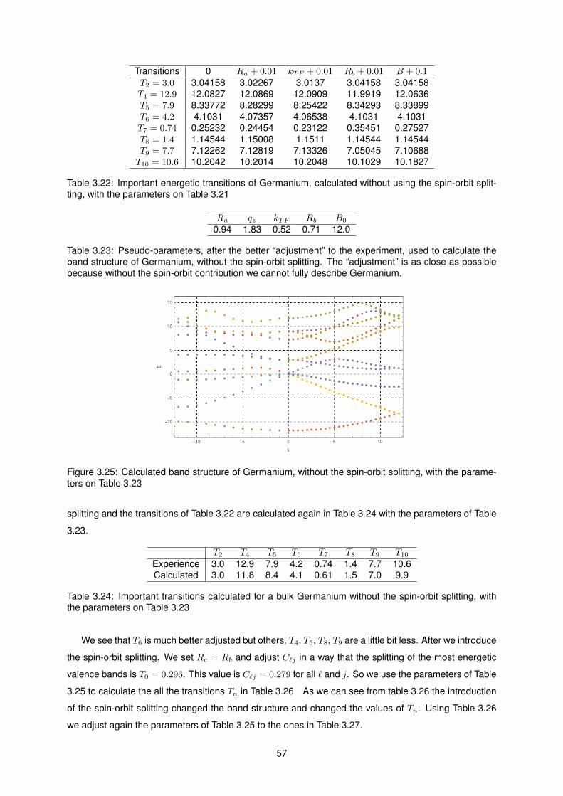
Transitions 0 Ra + 0.01 kTF + 0.01 Rb + 0.01 B + 0.1T2 = 3.0 3.04158 3.02267 3.0137 3.04158 3.04158T4 = 12.9 12.0827 12.0869 12.0909 11.9919 12.0636T5 = 7.9 8.33772 8.28299 8.25422 8.34293 8.33899T6 = 4.2 4.1031 4.07357 4.06538 4.1031 4.1031T7 = 0.74 0.25232 0.24454 0.23122 0.35451 0.27527T8 = 1.4 1.14544 1.15008 1.1511 1.14544 1.14544T9 = 7.7 7.12262 7.12819 7.13326 7.05045 7.10688T10 = 10.6 10.2042 10.2014 10.2048 10.1029 10.1827
Table 3.22: Important energetic transitions of Germanium, calculated without using the spin-orbit split-ting, with the parameters on Table 3.21
Ra qz kTF Rb B0
0.94 1.83 0.52 0.71 12.0
Table 3.23: Pseudo-parameters, after the better “adjustment” to the experiment, used to calculate theband structure of Germanium, without the spin-orbit splitting. The “adjustment” is as close as possiblebecause without the spin-orbit contribution we cannot fully describe Germanium.
Figure 3.25: Calculated band structure of Germanium, without the spin-orbit splitting, with the parame-ters on Table 3.23
splitting and the transitions of Table 3.22 are calculated again in Table 3.24 with the parameters of Table
3.23.
T2 T4 T5 T6 T7 T8 T9 T10
Experience 3.0 12.9 7.9 4.2 0.74 1.4 7.7 10.6Calculated 3.0 11.8 8.4 4.1 0.61 1.5 7.0 9.9
Table 3.24: Important transitions calculated for a bulk Germanium without the spin-orbit splitting, withthe parameters on Table 3.23
We see that T6 is much better adjusted but others, T4, T5, T8, T9 are a little bit less. After we introduce
the spin-orbit splitting. We set Rc = Rb and adjust C`j in a way that the splitting of the most energetic
valence bands is T0 = 0.296. This value is C`j = 0.279 for all ` and j. So we use the parameters of Table
3.25 to calculate the all the transitions Tn in Table 3.26. As we can see from table 3.26 the introduction
of the spin-orbit splitting changed the band structure and changed the values of Tn. Using Table 3.26
we adjust again the parameters of Table 3.25 to the ones in Table 3.27.
57

Ra qz kTF Rb B00 Rc C`j0.94 1.83 0.52 0.71 12.0 0.71 0.279
Table 3.25: This set of parameters are used to calculate important transitions of Germanium, with thespin-orbit splitting
Transitions Ra + 0.01 kTF + 0.01 Rb + 0.01 B00 + 0.1 Rc + 0.01 C`j + 0.1T0=0.296 0.295937 0.294133 0.295015 0.295937 0.295937 0.325729 0.38345T1=0.888 0.0409927 0.0784698 0.0588591 0.309062 0.0927434 0.0166953 0.146117T2=3.0 2.61454 2.59893 2.58871 2.61454 2.61454 2.57129 2.40364T3=0.21 0.227238 0.225022 0.225656 0.227238 0.227238 0.249606 0.406467T4=12.9 12.0424 12.0455 12.0514 11.9349 12.023 12.0667 12.0834T5=7.9 8.1037 8.05216 8.02233 8.10862 8.10473 8.07875 8.05465T6=4.2 3.80045 3.77378 3.7645 3.80046 3.80045 3.77077 3.69779T7=0.74 0.356431 0.353207 0.336776 0.484888 0.381147 0.331019 0.302728T8=1.4 1.27053 1.27433 1.27579 1.27052 1.27053 1.28317 1.22654T9=7.7 7.14404 7.14962 7.15642 7.06527 7.12927 7.16898 7.19284T10=10.6 10.1278 10.1236 10.1291 10.0082 10.106 10.1522 10.1703
Table 3.26: Important transitions of Germanium, including the spin-orbit splitting, are calculated from theparameters in Table 3.25
With this parameters we can plot and compare the separate potentials Vlocal(~k), ∆Vnonlocal(~k) and
∆Vspinorbit(~k) in Figure 3.26 with ~k going in the direction of X =(
1 0 0)
. Notice the widely different
Figure 3.26: The pseudopotentials a) Vlocal,screen(kx), b) ∆Vnonlocal(kx) and c) ∆Vspinorbit(kx) of Germa-nium are represented graphically, using the parameters of Table 3.27
vertical scales. We can see that the most important contribution for the electronic structure of the solid
is the local pseudopotential, followed by the non-local part and the spin-orbit pseudopotential, as it is
to be expected, since from equations (2.58) and (2.60), these potentials are treated as perturbations.
We can calculate the sum of the potentials above, plotted in Figure 3.27. We can see that the non-local
pseudopotential still has a significant effect. The effect of the spin-orbit contribution is very small but is
still enough to do the splitting of the last two valence p bands and the first two conduction p bands as we
can see in Figure 3.28.
The calculated the band “energies”, including those of 0.85X and X are shown in Figure 3.28 and in
Ra qz kTF Rb B00 Rc C`j0.94 1.83 0.52 0.74 12.0 0.71 0.279
Table 3.27: The set of parameters used to calculate the band structure of Germanium, with the spin-orbitsplitting are shown
58

Figure 3.27: The figure shows the different pseudopotential contributions Vlocal,screen(kx),Vlocal,screen(kx) + ∆Vnonlocal(kx) and Vlocal,screen(kx) + ∆Vnonlocal(kx) + ∆Vspinorbit(kx) of Germanium
Figure 3.28: Calculated band structure of Germanium, a) using reference [ea] (LDA) and with the exper-imental values of some important transitions in eV, b) with the program, using the parameters of Table3.27
Table 3.28. We observe that most of the values are much better fitted than previously.
T0 T1 T2 T3 T4 T5 T6 T7 T8 T9 T10 LB PRB32 PRB32Experience 0.296 0.888 3.0 0.21 12.9 7.9 4.2 0.74 1.4 7.7 10.6 1.3 3.5 9.5Calculated 0.296 0.882 2.6 0.23 11.7 8.1 3.8 0.76 1.3 6.9 9.8 1.0 2.9 8.1
Table 3.28: Important optical transitions of Germanium where calculated using the parameters of Table3.27
Afterwards we calculated D(E), J(E), ε1(ω), ε2ω and R(ω) in the same way we did before. We
calculated a grid of 7 × 7 × 7 points. The results are in Figure 3.29. We can compare this results with
the experiment from references [Che89] for D(E) and [AS83] for ε(ω) and R(ω), in the same Figure,
and observe that in both DOS graphics, the peaks are in the same place, but in the calculated DOS in
Figure 3.29 a) (and also the JDOS in b)), we have the noise of the Gaussians, that as mentioned before
would be fixed if we did Ni → +∞ and σ → 0. In the real part of the dielectric function, the calculated
peaks are slightly dislocated to higher energies of ∼ 0.5eV . About the imaginary part, in Figure c), we
59

indeed have one peak at ∼ 2.3eV and other at ∼ 4.2eV , but they have different intensities. The rest of
the Figure c) hardly agrees with the experiment. About the reflectance, we can see in Figure d), that the
peak at ∼ 4.5eV is dislocated to a higher energy. The calculated Figures are very affected by the small
number of points in the grid.
60

Figure 3.29: It is represented a) the calculated density if states (blue line),the photo emission spec-troscopy and inverse photo emission data obtained from reference [Che89] (yellow line) divided by afactor of 3, b) the calculated joint density of states, c) calculated dielectric function, real part (blue) andimaginary (purple), d) calculated (blue line) and experimental (yellow line, [AS83]) ε1, e) calculated (blueline) and experimental (yellow line, [AS83]) ε2 f),g) calculated (blue line) and experimental (yellow line,[AS83]) reflectance for Germanium with the local pseudopotential of equation (3.7), the non-local projec-tor for the pseudopotential of equation (3.19) with the parameters written in Table 3.9 and the spin-orbitprojectors using equations (2.74) and (3.25-3.27) with lmax = 2
61

62

Chapter 4
Conclusions
In this research project we obtained a description of bulk Silicon, Carbon and Germanium, group IV el-
ements, using the Empirical Pseudopotential Method. We obtained a successful description for Silicon,
since the band structure was pretty well adjusted, and we did that by using parameters in a pseudopoten-
tial model that have physical meaning. The reflectance and the imaginary part of the dielectric function
could be better, but the calculation of this properties allowed us to diagnose a problem with the band
structure that was drawn. As a future work, the pseudopotential should also be adjusted to the experi-
mental reflectance data, which seems to promise a better success. Also the fact that we used a small
number of points aggravated our predictions for the optical properties of Silicon, because, since we used
the MATHEMATICA software, we could not use a big number of points without costing a lot of time to do
the calculations. For Germanium, the results are similar to Silicon. The band structure and the density of
states was pretty well adjusted to the experimental values, but in the future we should also try to adjust
to the optical properties such as reflectance, to obtain better results. To Carbon (Diamond), we obtained
the least successful description, since it was very difficult to adjust the band structure with just a small
number of parameters. This element requires some extra work and, in the future the research could go
into finding a pseudopotential model with more parameters to describe it.
All the tools where developed to continue this research and improve each of the descriptions. As
a next step we can introduce the pseudopotentials in a FORTRAN program and increase the number of
points in the cubic grid, to obtain better results. Using the parameters found here, we already did that, as
we can see in Figure 4.1 for Silicon, Figure 4.2 for Carbon and Figure 4.3 for Germanium. We compare
the obtained band structure and density of states with a DFT-MGGA (Density Functional Theory with a
Meta Generalized Gradient Approximation). DFT-MGGA is right now a state of the art ab initio theory
but still doesn’t give the right gaps to semiconductors. We can see in the figures that we have much
better results only by adding a lot more points in the grid.
After having the best description possible of each of the elements, as a future research the pseu-
dopotentials will be used to be introduced in a supercell composed with these elements. This was
already tested for a Si29C supercell, a supercell of Si with a C impurity. Figure 4.4 shows the calculated
unfolded band structure for that system.
63

Figure 4.1: The figure shows the a) band structure and the b) density of states, calculated for Siliconusing the pseudopotentials obtained here and using a DFT-MGGA calculation
Figure 4.2: The figure shows the a) band structure and the b) density of states, calculated for Carbonusing the pseudopotentials obtained here and using a DFT-MGGA calculation
Figure 4.3: The figure shows the a) band structure and the b) density of states, calculated for Germaniumusing the pseudopotentials obtained here and using a DFT-MGGA calculation
With an improvement of the fit to the optical properties, these EPM could be used to search for the
material with the best optoelectronic properties that is compatible with Si technology.
64

Figure 4.4: The figure shows the unfolded band structure of Si29C
65

66

Bibliography
[AG00] Martin Stadele Aulbur, Wilfried G. and Andreas Gorling. Exact-exchange-based quasiparticle
calculations. Physical Review B, 62(11), 7121, 2000.
[All10] Alloul, Henri, and Stephen Lyle. Introduction to the Physics of Electrons in Solids. Springer,
2010.
[AM76] Neil W. Ashcroft and N. David Mermin. Solid State Physics. Saunders College, Philadelphia,
1976.
[AS83] D. E. Aspnes and A. A. Studna. Dielectric functions and optical parameters of si, ge, gap, gaas,
gasb, inp, inas, and insb from 1.5 to 6.0 ev. Physical Review B, 27(2), 985, 1983.
[BH88] Max Born and Kun Huang. Dynamical Theory of Crystal Lattices. Clarendon Press, Oxford,
1988.
[CC92] James R. Chelikowsky and Marvin L. Cohen. Ab initio pseudopotentials and the structural
properties of semiconductors. Handbook on Semiconductors, ed. PT Landsberg, Elsevier, Am-
sterdam 1, 1992.
[Che89] Weaver Jin Chelikowsky, Wagener. Valence- and conduction-band densities of states for tetra-
hedral semiconductors: Theory and experiment. Physical Review B, 40(14), 9644, 1989.
[Che96] James R. Chelikowsky. Empirical Pseudopotentials for Semiconductors. KLUWER INTERNA-
TIONAL SERIES IN ENGINEERING AND COMPUTER SCIENCE, 39-52, 1996.
[d’A12] Luo J. W. Chanier T. & Zunger A. d’Avezac, M. Genetic-algorithm discovery of a direct-gap and
optically allowed superstructure from indirect-gap Si and Ge semiconductors. Physical Review
Letters, 108(2), 027401., 2012.
[ea] Jose Luıs Martins et all. Program for calculation of the band structure using ab initio lda pseu-
dopotentials.
[ea74] McFeely et al. X-ray photoemission studies of diamond, graphite, and glassy carbon valence
bands. Physical Review B, 9(12), 5268, 1974.
[KB82] Leonard Kleinman and D. M. Bylander. Efficacious form for model pseudopotentials. Physical
Review Letters, 48(20), 1425, 1982.
67

[Kit76] Kittel, Charles, and Paul McEuen. Introduction to solid state physics. New York: Wiley, 1976.
[Kle80] Leonard Kleinman. Relativistic norm-conserving pseudopotential. Physical Review B, 21(6),
2630, 1980.
[KS65] Walter Kohn and Lu Jeu Sham. Self-consistent equations including exchange and correlation
effects. Physical Review, 140(4A), A1133, 1965.
[Lan80] Landau, L. D., and E. M. Lifshitz. Statistical physics, vol. 5. Course of theoretical physics 30,
1980.
[Lie83] Elliott H. Lieb. Density functionals for coulomb systems. International Journal of Quantum
Chemistry, 24(3), 243, 1983.
[Mar] Jose Luıs Martins. Unpublished lecture notes in condensed matter physics.
[New84] & Dow J. D. Newman, K. E. Theory of deep impurities in silicon-germanium alloys. Physical
Review B, 30(4), 1929, 1984.
[Ost98] H. J. Osten. Band-gap changes and band offsets for ternary Si1−x−yGexCy alloys on Si (001).
Journal of applied physics, 84(5), 2716-2721, 1998.
[Pea87] et al. Pearsall, T. P. Structurally induced optical transitions in Ge-Si superlattices. Physical
review letters, 58(7), 729, 1987.
[PW92] John P. Perdew and Yue Wang. Accurate and simple analytic representation of the electron-gas
correlation energy. Physical Review B, 45(23), 13244, 1992.
[RW67] Roberts and Walker. Optical Study of the Electronic Structure of Diamond. Physical Review,
161(3), 730, 1967.
[SB51] E. E. Salpeter and H. A. Bethe. A Relativistic Equation for Bound-State Problems. Physical
Review, 84(6), 1232, 1951.
[Sch91] Christensen N. E. Alouani M. & Cardona M. Schmid, U. Electronic and optical properties of
strained Ge/Si superlattices. Physical Review B, 43(18), 14597, 1991.
[SF] N. Troulier S Froyen. A pseudopotential generation program.
[TB09] Fabien Tran and Peter Blaha. Accurate band gaps of semiconductors and insulators with a
semilocal exchange-correlation potential. Physical Review Letters, 102(22), 226401, 2009.
[TH01] Gerhard Theurich and Nicola A. Hill. Self-consistent treatment of spin-orbit coupling in solids
using relativistic fully separable ab initio pseudopotentials. Physical Review B, 64(7), 073106,
2001.
[TM91] Norman Troullier and Jose Luıs Martins. Efficient pseudopotentials for plane-wave calculations.
Physical Review B, 43(3), 1993, 1991.
68
[TT93] H. M. Polatoglou Tserbak, C. and G. Theodorou. Unified approach to the electronic structure of
strained Si/Ge superlattices. Physical Review B, 47(12), 7104, 1993.
[WZ95] Lin-Wang Wang and Alex Zunger. Local-density-derived semiempirical pseudopotentials. Phys-
ical Review B, 51(24), 17398, 1995.
[Yu,96] Yu, Peter Y., and Manuel Cardona. Fundamentals of semiconductors. Springer, 1996.
[Zak01] et al Zakharov, N. D. Structure and optical properties of Ge/Si superlattice grown at Si substrate
by MBE at different temperatures. Materials Science and Engineering: B 87(1), 92-95, 2001.
69

70

Appendix A
Clebsch-Gordon coefficients for
mixing states ` and s = 12
We want to calculate the Clebsh-Gordon coefficients for the total angular momentum j when we have a
state with orbital l and spin s = 12 angular momenta. To do so, we se the raising and lowering operators,
J±, the operators Jx = 12 (J+ + J−), Jy = 1
2i (J+ − J−) and Jz, and also the J2 operator.
When we apply the J± operators to a state |j mj〉 the results are
J+ |j mj〉 =~2
√j(j + 1)−mj(mj + 1) |j mj + 1〉 (A.1)
J− |j mj〉 =~2
√j(j + 1)−mj(mj − 1) |j mj − 1〉 . (A.2)
With the Jx,y operators
Jx |j mj〉 =1
2[J+ |j mj〉+ J− |j mj〉] =
=~2
[√j(j + 1)−mj(mj + 1) |j mj + 1〉+
√j(j + 1)−mj(mj − 1) |j mj − 1〉
](A.3)
Jy |j mj〉 =1
2i[J+ |j mj〉 − J− |j mj〉] =
=~2i
[√j(j + 1)−mj(mj + 1) |j mj + 1〉 −
√j(j + 1)−mj(mj − 1) |j mj − 1〉
]. (A.4)
and the Jz and J2 operators
Jz |j mj〉 = ~mj |j mj〉 (A.5)
J2 |j mj〉 = ~2j(j + 1) |j mj〉 . (A.6)
Using the rules of the addition of angular momenta for ~J = ~L + ~S, the quantum numbers satisfy for
s = 12
∣∣∣∣`− 1
2
∣∣∣∣ < j < `+1
2. (A.7)
For ` = 0, the only allowed value for j is j = 12 . For the other cases
71

`−1
2< j < `+
1
2, (A.8)
which means that the allowed values for j are j = ` − 12 and j = ` + 1
2 . The z projections of the
momenta always satisfy mj = m` +ms with ms = ± 12 . So, the state |j mj〉 can be described by a linear
combination of the states∣∣`mj − 1
2
⟩ ∣∣ 12
12
⟩and
∣∣`mj + 12
⟩ ∣∣ 12 −
12
⟩|j mj〉 = A
∣∣∣∣`mj − 1
2
⟩ ∣∣∣∣12 1
2
⟩+B
∣∣∣∣`mj +1
2
⟩ ∣∣∣∣12 − 1
2
⟩. (A.9)
First we apply the J2 operator, for which:
J2 = L2 + S2 + 2~L · ~S~L = Lx~ex + Ly~ey + Lz~ez
~S = Sx~ex + Sy~ey + Sz~ez
~L · ~S = LxSx + LySy + LzSz
J2 = L2 + S2 + 2(LxSx + LySy + LzSz). (A.10)
Applying eq. (A.10) to the |j mj〉 state, we have that:
J2 |j mj〉 =[L2 + S2 + 2(LxSx + LySy + LzSz)
] [A
∣∣∣∣`mj − 1
2
⟩ ∣∣∣∣12 1
2
⟩+B
∣∣∣∣`mj +1
2
⟩ ∣∣∣∣12 − 1
2
⟩]=
= A
(L2
∣∣∣∣`mj − 1
2
⟩) ∣∣∣∣12 1
2
⟩+
∣∣∣∣`mj − 1
2
⟩(S2
∣∣∣∣12 1
2
⟩)+
+2
[(Lx
∣∣∣∣`mj − 1
2
⟩)(Sx
∣∣∣∣12 1
2
⟩)+
(Ly
∣∣∣∣`mj − 1
2
⟩)(Sy
∣∣∣∣12 1
2
⟩)+
+
(Lz
∣∣∣∣`mj − 1
2
⟩)(Sz
∣∣∣∣12 1
2
⟩)]+ B
(L2
∣∣∣∣`mj +1
2
⟩) ∣∣∣∣12 − 1
2
⟩+
∣∣∣∣`mj +1
2
⟩(S2
∣∣∣∣12 − 1
2
⟩)+
+2
[(Lx
∣∣∣∣`mj +1
2
⟩)(Sx
∣∣∣∣12 − 1
2
⟩)+
(Ly
∣∣∣∣`mj +1
2
⟩)(Sy
∣∣∣∣12 − 1
2
⟩)+
+
(Lz
∣∣∣∣`mj +1
2
⟩)(Sz
∣∣∣∣12 − 1
2
⟩)].
Using equations (A.3) to (A.6) and since the states∣∣ 1
2 ,±32
⟩do not exist (because ms only has values
from −s to s) we have:
J2 |j mj〉 = A
3
4~2∣∣∣∣12 1
2
⟩ ∣∣∣∣`mj − 1
2
⟩+ ~2l(l + 1)
∣∣∣∣12 1
2
⟩ ∣∣∣∣`mj − 1
2
⟩+
+2
[~2
∣∣∣∣12 − 1
2
⟩~2
(√`(`+ 1)−
(mj −
1
2
)(mj +
1
2
) ∣∣∣∣`mj +1
2
⟩+
+
√`(`+ 1)−
(mj −
1
2
)(mj −
3
2
) ∣∣∣∣`mj − 3
2
⟩)+
+i~2
∣∣∣∣12 − 1
2
⟩~2i
(√`(`+ 1)−
(mj −
1
2
)(mj +
1
2
) ∣∣∣∣`mj +1
2
⟩+
−
√`(`+ 1)−
(mj −
1
2
)(mj −
3
2
) ∣∣∣∣`mj − 3
2
⟩)+
+~2
∣∣∣∣12 1
2
⟩~(mj −
1
2)
∣∣∣∣`mj − 1
2
⟩]+
B
3
4~2∣∣∣∣12 − 1
2
⟩ ∣∣∣∣`mj +1
2
⟩+ ~2`(`+ 1)
∣∣∣∣12 − 1
2
⟩ ∣∣∣∣`mj +1
2
⟩+
+2
[~2
∣∣∣∣12 1
2
⟩~2
(√`(`+ 1)−
(mj +
1
2
)(mj +
3
2
) ∣∣∣∣`mj +3
2
⟩+
+
√`(`+ 1)−
(mj +
1
2
)(mj −
1
2
) ∣∣∣∣`mj − 1
2
⟩)+
72

+i~2
∣∣∣∣12 1
2
⟩~2i
(√`(`+ 1)−
(mj +
1
2
)(mj +
3
2
) ∣∣∣∣`mj +3
2
⟩+
−
√`(`+ 1)−
(mj +
1
2
)(mj −
1
2
) ∣∣∣∣`mj − 1
2
⟩)+
−~2
∣∣∣∣12 − 1
2
⟩~(mj +
1
2)
∣∣∣∣`mj +1
2
⟩]. (A.11)
As we said before, in eq. (A.9), the state |j mj〉 is only described by∣∣`mj − 1
2
⟩ ∣∣ 12
12
⟩and
∣∣`mj + 12
⟩ ∣∣ 12 −
12
⟩states, which means the
∣∣`mj ± 32
⟩are not present:
J2 |j mj〉 = ~2A
[3
4+ `(`+ 1) +mj −
1
2
]+B
√`(`+ 1)−m2
j +1
4
∣∣∣∣12 1
2
⟩ ∣∣∣∣`mj − 1
2
⟩+
~2B
[3
4+ `(`+ 1)−mj −
1
2
]+A
√`(`+ 1)−m2
j +1
4
∣∣∣∣12 − 1
2
⟩ ∣∣∣∣`mj +1
2
⟩, (A.12)
but also
J2 |j mj〉 = ~2j(j + 1) |j mj〉
= ~2j(j + 1)
[A
∣∣∣∣`mj − 1
2
⟩ ∣∣∣∣12 1
2
⟩+B
∣∣∣∣`mj +1
2
⟩ ∣∣∣∣12 − 1
2
⟩]. (A.13)
So we have the system of equations:
A[`(`+ 1) + 1
4+mj
]+ B
√`(`+ 1)−m2
j + 14
= j(j + 1)A
B[`(`+ 1) + 1
4−mj
]+ A
√`(`+ 1)−m2
j + 14
= j(j + 1)B⇔
⇔
A[`(`+ 1)− j(j + 1) + 1
4+mj
]+ B
√`(`+ 1)−m2
j + 14
= 0
B[`(`+ 1)− j(j + 1) + 1
4−mj
]+ A
√`(`+ 1)−m2
j + 14
= 0⇔
⇔
A(a+mj) + Bb = 0
B(a−mj) + Ab = 0with
a = `(`+ 1)− j(j + 1) + 14
b =√`(`+ 1)−m2
j + 14
. (A.14)
Multiplying the first equation of the system by (a−mj) and the second by b we have
A(a2 −m2j ) + Bb(a−mj) = 0
Bb(a−mj) + Ab2 = 0. (A.15)
Subtracting the second equation from the first one:
A(a2 −m2j − b2) = 0⇔ a2 − b2 = m2
j ⇔
⇔[`(`+ 1)− j(j + 1) +
1
4
]2− `(`+ 1) +m2
j −1
4= m2
j ⇔
⇔[`(`+ 1)− j(j + 1) +
1
4
]2= `2 + `+
1
4=
(`+
1
2
)2
⇔
⇔ `(`+ 1)− j(j + 1) +1
4= ±
(`+
1
2
)⇔
⇔ j(j + 1) = `(`+ 1)∓(`+
1
2
)+
1
4⇔ . (A.16)
Adding 14 to both sides of the equation:
j2 + j +1
4= `(`+ 1)∓
(`+
1
2
)+
1
2⇔(j +
1
2
)2
=
`2 + `− `− 12
+ 12
= `2
`2 + `+ `+ 12
+ 12
= (`+ 1)2⇔
73

⇔
j + 12
= ±`
j + 12
= ±(`+ 1)⇔
j = ±`− 1
2=
`− 12
−`− 12
j + 12
= ±(`+ 1)− 12
=
`+ 12
−`− 32
. (A.17)
But we know that j ≥ 0 so the only good values are j = ± 12 .
Having this result, we have that the values for a and b are:
a = `2 + `−(`±
1
2
)(`±
1
2+ 1
)+
1
4=
= `2 + `− `2 ∓1
2`− `∓
1
2`−
1
4∓
1
2+
1
4=
= ∓`∓1
2= ∓(`+
1
2) (A.18)
b =
√(`2 + `+
1
4
)−m2
j =
√(`+
1
2
)2
−m2j =
=
√(`+
1
2+mj
)(`+
1
2−mj
). (A.19)
Putting this in eq. (A.14):
A
[∓(`+
1
2
)+mj
]= ∓A
(`+
1
2∓mj
)= −B
√(`+
1
2+mj
)(`+
1
2−mj
)⇔
⇔ A
√`+
1
2∓mj = ±B
√`+
1
2±mj ⇔ |A|2
(`+
1
2∓mj
)= |B|2
(`+
1
2±mj
). (A.20)
But |A|2 + |B|2 = 1
|A|2(`+
1
2∓mj
)= (1− |A|2)
(`+
1
2±mj
)⇔ |A|2
`+ 12∓mj
`+ 12±mj
= 1− |A|2 ⇔
⇔ |A|2(
1 +`+ 1
2∓mj
`+ 12±mj
)= 1⇔ |A|2
`+ 12±mj + `+ 1
2∓mj
`+ 12±mj
=2`+ 1
`+ 12±mj
= 1. (A.21)
The Clebsch-Gordon coefficents are always real, and using the phase convention⟨` 1
2 ; ` 12
∣∣ `+ 12 `+ 1
2
⟩≥
0, A has to be bigger than 0, so
A =
√`+ 1
2±mj
2`+ 1=
√2`+ 1± 2mj
4`+ 2. (A.22)
We can now calculate B:
A
√`+
1
2∓mj = ±B
√`+
1
2±mj ⇔ B = ±A
√`+ 1
2±mj√
`+ 12∓mj
= ±
√2`+ 1∓mj
2`+ 1, (A.23)
for which the upper and lower signs correspond to j = `± 12 .
74

Appendix B
Spin-Orbit projectors for the
pseudopotential
We start with the psedopotential on the Kleinman-Bylander form considering the spin,
VKB =∑`,j,mj
∣∣∣∆V SO`,j ΦPP`,j,mj
⟩⟨ΦPP`,j,mj
∆V SO`,j
∣∣∣⟨ΦPP`,j,mj
∣∣∣∆V SO`,j
∣∣∣ΦPP`,j,mj⟩ , (B.1)
where∣∣∣ΦPP`,j,mj⟩ = 1√
2R`j
Y`mj− 12(θ, φ)
Y`mj+ 12(θ, φ)
is the atomic spin orbit eigenfunction, and rewrite it in an
other way:
VKB =∑`,j,mj
∣∣∣∆V SO`,j ΦPP`,j,mj
⟩sgn(⟨
ΦPP`,j,mj
∣∣∣∆V SO`,j
∣∣∣ΦPP`,j,mj⟩)⟨ΦPP`,j,mj∆V SO
`,j
∣∣∣∣∣∣⟨ΦPP`,j,mj
∣∣∣∆V SO`,j
∣∣∣ΦPP`,j,mj⟩∣∣∣ =
=∑`,j,mj
∣∣∣∆V SO`,j ΦPP`,j,mj
⟩√∣∣∣⟨ΦPP`,j,mj
∣∣∣∆V SO`,j
∣∣∣ΦPP`,j,mj⟩∣∣∣sgn(⟨
ΦPP`,j,mj
∣∣∣∆V SO`,j
∣∣∣ΦPP`,j,mj⟩)⟨
ΦPP`,j,mj∆V SO
`,j
∣∣∣√∣∣∣⟨ΦPP`,j,mj
∣∣∣∆V SO`,j
∣∣∣ΦPP`,j,mj⟩∣∣∣.(B.2)
The value of b`j is
b`j =⟨
ΦPP`,j,mj
∣∣∣∆V SO`,j
∣∣∣ΦPP`,j,mj⟩=
∫ 2π
0
∫ π
0
∫ +∞
0R∗`j(r)
1√
2
(Y ∗`mj− 1
2
(θ, φ) Y ∗`mj+
12
(θ, φ)
)∆V SO`j (r)R`j(r)
1√
2
Y`mj− 12
(θ, φ)
Y`mj+ 12
(θ, φ)
r2 sin θdrdθdφ =
=1
2
∫ 2π
0
∫ π
0[Y ∗`mj− 1
2
(θ, φ)Y`mj− 12
(θ, φ) + Y ∗`mj+
12
(θ, φ)Y`mj+ 12
(θ, φ)] sin θdθdφ
∫ +∞
0R∗`j(r)∆V
SO`j (r)R`j(r)r
2dr =
=
∫ +∞
0R∗`j(r)∆V
SO`j (r)R`j(r)r
2dr, (B.3)
where Y`m are the spherical harmonic functions and we used m = mj −ms, where ms = ± 12 is the spin
angular momentum. It is independent of mj . The potential is, therefore,
VKB =∑`,j,mj
∣∣∣∆V SO`,j ΦPP`,j,mj
⟩√|b`j |
sgn(b`j)
⟨ΦPP`,j,mj
∆V SO`,j
∣∣∣√|b`j |
, (B.4)
and we define the “projector” spinor a`jmj as
75

∣∣∣a`,j,mj⟩ =
∣∣∣∆V SO`,j ΦPP`,j,mj
⟩√|b`j |
. (B.5)
and thus we have,
VKB =∑`,j,mj
∣∣∣a`,j,mj⟩ sgn(b`j)⟨a`,j,mj
∣∣∣ . (B.6)
Therefore, the functions of the projectors are
a`jmj (r, θ, φ) =1√
2|b`j |∆V SO
`,j (r)R`j(r)
Y`mj− 12
(θ, φ)
Y`mj+ 12
(θ, φ)
. (B.7)
76

Appendix C
Matrix elements of the momentum
matrix operator between plane waves
Considering a semiconductor crystal, a plane wave basis set is used for the wave functions inside the
crystal
⟨~r∣∣∣ ~kn, n⟩ =
1√Vcrystal
ei~kn·~r, (C.1)
where the position vector ~r inside the crystal is defined by
~r = y1N1~a1 + y2N2~a2 + y3N3~a3, (C.2)
with 0 < yn < 1 and ~ai are the primitive lattice vectors, and in the reciprocal lattice,
~k =i1
N1
~b1 +i2
N2
~b2 +i3
N3
~b3 (C.3)
with ij = 0, . . . , Nj−1 and~bi are the primitive reciprocal lattice vectors. Vcell = ~a1 ·(~a2×~a3) is the volume
of the primitive cell and the whole crystal has the size N1~a1 ×N2~a2 ×N3~a3. To write the basis functions
for the free electrons in the conduction and valence bands, we use in equation (C.1), n = c and n = v
respectively. We now calculate the matrix element
⟨~kc, nc
∣∣∣~e · ~p ∣∣∣~kv , nv⟩ = −i⟨~kc, nc
∣∣∣~e · ~∇ ∣∣∣~kv , nv⟩= −i
1
Vcrystal
∫∫∫crystal
e−i~kc·~r(~e · ~∇)ei
~kv·~rd3r
= −i1
Vcrystal
∫∫∫crystal
e−i~kc·~r(~e · ~kv)ei
~kv·~rd3r
=~e · ~kvVcrystal
∫∫∫crystal
e−i~kc·~rei
~kv·~rd3r
=~e · ~kvVcrystal
∫∫∫crystal
ei(~kv−~kc)·~rd3r. (C.4)
By making the change of variables ~r = y1N1~a1 + y2N2~a2 + y3N3~a3,
∫∫∫crystal
d3~r = C
∫ 1
0dy1
∫ 1
0dy2
∫ 1
0dy3 ⇔ Vcrystal = C, (C.5)
and replacing ~k for (C.3),
77

⟨~kc, nc
∣∣∣~e · ~p ∣∣∣~kv , nv⟩ =~e · ~kvVcrystal
Vcrystal
∫ 1
0
∫ 1
0
∫ 1
0ei(i1v−i1cN1
~b1+i2v−i2cN2
~b2+i3v−i3cN3
~b3)·(y1N1~a1+y2N2~a2+y3N3~a3)dy1dy2dy3.
(C.6)
Since⟨~ai
∣∣∣ ~bj⟩ = 2πδij ,
⟨~kc, nc
∣∣∣~e · ~p ∣∣∣~kv , nv⟩ =~e · ~kvVcrystal
Vcrystal
∫ 1
0ei2π(i1v−i1c)y1dy1
∫ 1
0ei2π(i2v−i2c)y2dy2
∫ 1
0ei2π(i3v−i3c)y3dy3 =
= ~e · ~kv
[ei2π(i1v−i1c)y1
i2π(i1v − i1c)
]10
×[ei2π(i2v−i2c)y2
i2π(i2v − i2c)
]10
×[ei2π(i3v−i3c)y3
i2π(i3v − i3c)
]10
=
= ~e · ~kvei2π(i1v−i1c) − 1
i2π(i1v − i1c)×ei2π(i2v−i2c) − 1
i2π(i2v − i2c)×ei2π(i3v−i3c) − 1
i2π(i3v − i3c)=
= ~e · ~kvcos[2π(i1v − i1c)] + i sin[2π(i1v − i1c)]− 1
i2π(i1v − i1c)×
×cos[2π(i2v − i2c)] + i sin[2π(i2v − i2c)]− 1
i2π(i2v − i2c)×
×cos[2π(i3v − i3c)] + i sin[2π(i3v − i3c)]− 1
i2π(i3v − i3c). (C.7)
Since 2π(inv − inc) is an integer multiplied by 2π, the value of the cos function with this argument is
1, while the sin is always 0. Therefore, if ~kc 6= ~kv,⟨~kc, nc
∣∣∣~e · ~p ∣∣∣~kv, nv⟩ = 0. If ~kc = ~kv,
⟨~kc, nc
∣∣∣~e · ~p ∣∣∣~kv , nv⟩ =~e · ~kvVcrystal
∫∫∫crystal
d3r =~e · ~kvVcrystal
Vcrystal = ~e · ~kv (C.8)
78

Appendix D
Orthogonality of the basis functions
We have a 3-dimensional crystal with primitive lattice vectors ~aj , Natom atoms in the primitive cell with
atomic positions ~τi. The reciprocal lattice vectors are
~b1 = 2π~a2 × ~a3Vcell
~b2 = 2π~a3 × ~a1Vcell
~b3 = 2π~a1 × ~a2Vcell
(D.1)
with Vcell = ~a1 · (~a2 × ~a3) being the volume of the primitive cell. The whole crystal has the size N1~a1 ×
N2~a2 ×N3~a3.The position vector ~r inside the crystal is defined by
~r = y1N1~a1 + y2N2~a2 + y3N3~a3 (D.2)
with 0 < yn < 1 and in the reciprocal lattice:
~ki1i2i3 =i1
N1
~b1 +i2
N2
~b2 +i3
N3
~b3 (D.3)
with ij = 0, . . . , Nj − 1. The reciprocal lattice vectors ~G (the vectors that yield plane waves with theperiodicity of the Bravais lattice) are defined:
~G = I1~b1 + I2~b2 + I3~b3 (D.4)
A plane wave basis set is used for the wave functions inside the crystal:
⟨~r∣∣∣ ~ki1i2i3 , ~GI1I2I3⟩ =
1√N1N2N3Vcell
ei(~ki1i2i3+~GI1I2I3 )·~r (D.5)
We can prove they are orthogonal for different vectors ~ki1i2i3 and ~GI1I2I3 . Here we show a lengthy
but detailed derivation, using a normalization in the crystal.
⟨~k′i′1i
′2i′3, ~G′I′1I
′2I′3
∣∣∣ ~ki1i2i3 , ~GI1I2I3⟩ =
∫∫∫crystal
1√N1N2N3Vcell
e−i(~k′
i′1i′2i′3+~G′
I′1I′2I′3)·~r 1√N1N2N3Vcell
ei(~ki1i2i3+
~GI1I2I3 )·~rd3~r =
=1
N1N2N3Vcell
∫∫∫crystal
ei(~ki1i2i3−
~k′i′1i′2i′3)·~rei(~GI1I2I3−
~G′I′1I′2I′3)d3~r (D.6)
If ~ki1i2i3 = ~k′i′1i′2i′3and ~GI1I2I3 = ~G′I′1I′2I′3
⟨~k′i′1i
′2i′3, ~G′I′1I
′2I′3
∣∣∣ ~ki1i2i3 , ~GI1I2I3⟩ =1
N1N2N3Vcell
∫crystal
1d3~r
=1
N1N2N3VcellN1N2N3Vcell = 1 (D.7)
79

If not, we can make the change of variables ~r = y1N1~a1 + y2N2~a2 + y3N3~a3
∫∫∫crystal
d3~r = C
∫ 1
0dy1
∫ 1
0dy2
∫ 1
0dy3 ⇔ N1N2N3Vcell = C (D.8)
⟨~k′i′1i
′2i′3, ~G′I′1I
′2I′3
∣∣∣ ~ki1i2i3 , ~GI1I2I3⟩ =1
N1N2N3VcellN1N2N3Vcell×
×∫ 1
0
∫ 1
0
∫ 1
0ei(i1−i
′1
N1~b1+
i2−i′2
N2~b2+
i3−i′3
N3~b3)·(y1N1~a1+y2N2~a2+y3N3~a3)×
×ei((I1−I′1)~b1+(I2−I′2)~b2+(I3−I′3)~b3)·(y1N1~a1+y2N2~a2+y3N3~a3)dy1dy2dy3 =
=
∫ 1
0ei2π(i1−i
′1+(I1−I′1)N1)y1dy1
∫ 1
0ei2π(i2−i
′2+(I2−I′2)N2)y2dy2
∫ 1
0ei2π(i3−i
′3+(I3−I′3)N3)y3dy3 =
=
[ei2π(i1−i
′1+(I1−I′1)N1)y1
i2π(i1 − i′1 + (I1 − I′1)N1)
]10
×[ei2π(i2−i
′2+(I2−I′2)N2)y2
i2π(i2 − i′2 + (I2 − I′2)N2)
]10
×[ei2π(i3−i
′3+(I3−I′3)N3)y3
i2π(i3 − i′3 + (I3 − I′3)N3)
]10
=
=ei2π(i1−i
′1+(I1−I′1)N1) − 1
i2π(i1 − i′1 + (I1 − I′1)N1)×ei2π(i2−i
′2+(I2−I′2)N2) − 1
i2π(i2 − i′2 + (I2 − I′2)N2)×ei2π(i3−i
′3+(I3−I′3)N3) − 1
i2π(i3 − i′3 + (I3 − I′3)N3)=
=cos [2π(i1 − i′1 + (I1 − I′1)N1)] + i sin [2π(i1 − i′1 + (I1 − I′1)N1)]− 1
i2π(i1 − i′1 + (I1 − I′1)N1)×
×cos [2π(i2 − i′2 + (I2 − I′2)N2)] + i sin [2π(i2 − i′2 + (I2 − I′2)N2)]− 1
i2π(i2 − i′2 + (I2 − I′2)N2)×
×cos [2π(i3 − i′3 + (I3 − I′3)N3)] + i sin [2π(i2 − i′2 + (I2 − I′2)N2)]− 1
i2π(i3 − i′3 + (I3 − I′3)N3)(D.9)
Since we have in the argument of the co-sinus and sinus functions, i2π(in − i′n + In − I ′n)Nn, which
is an integer number multiplied by 2π, the cos function will be equal to 1, while the sin will be zero.
Therefore, if in 6= i′n and In 6= I ′n we have that⟨~k′i′1i′2i′3
, ~G′I′1I′2I′3
∣∣∣ ~ki1i2i3 , ~GI1I2I3⟩ = 0, so in conclusion:
⟨~k′i′1i
′2i′3, ~G′I′1I
′2I′3
∣∣∣ ~ki1i2i3 , ~GI1I2I3⟩ = δi1i′1δi2i′2
δi3i′3δI1I′1
δI2I′2δI3I′3
= δ~ki1i2i3~k′i′1i′2i′3
δ~GI1I2I3~G′I′1I′2I′3
(D.10)
80

Appendix E
Pseudopotentials matrix elements
E.1 Local Pseudopotencial
Here we show an accurate derivation of the matrix elements of the local pseudopotential, with normal-
ization in the crystal.
For a crystal with primitive lattice vectors ~aj , Natom atoms in the primitive cell with atomic positions
τi, and dimensions Nj~aj , the local pseudopotential is given by
V (L)(~r) =∑J1∈Z
∑J2∈Z
∑J3∈Z
N1−1∑j1=0
N2−1∑j2=0
N3−1∑j3=0
Natom∑i=1
v(L)(~r − ~tj1j2j3 − ~TJ1J2J3 − ~τi) (E.1)
where
~tj1j2j3 = j1~a1 + j2~a2 + j3~a3
~TJ1J2J3 = J1N1~a1 + J2N2~a2 + J3N3~a3 (E.2)
are the translation vectors for the finite crystal and for its periodic crystal images. The matrix elements
of the pseudopotential in a plane wave basis set
⟨~r∣∣∣ ~ki1i2i3 , ~GI1I2I3⟩ =
1√N1N2N3Vcell
ei(~ki1i2i3+~GI1I2I3 )·~r (E.3)
with ~ki1i2i3 = i1N1
~b1 + i2N2
~b2 + i3N3
~b3, with ij = 0, . . . , Nj − 1, a vector in the primitive reciprocal unit celland ~GI1I2I3 = I1~b1 + I2~b2 + I3~b3 with Ij ∈ Z a reciprocal lattice vector, are⟨
~k′i′1i′2i′3, ~G′I′1I
′2I3
∣∣∣V (L)∣∣∣~ki1i2i3 , ~GI1I2I3⟩ =
=
∫∫∫crystal
1√N1N2N3Vcell
e−i(~k′
i′1i′2i′3+~G′
I′1I′2I3
)·~rV (L)(~r)
1√N1N2N3Vcell
ei(~ki1i2i3+~GI1I2I3 )·~rd3~r =
=1
N1N1N3Vcell
∫∫∫crystal
e−i(~k′
i′1i′2i′3+~G′
I′1I′2I3
)·~r×
×
∑J1∈Z
∑J2∈Z
∑J3∈Z
N1−1∑j1=0
N2−1∑j2=0
N3−1∑j3=0
Natom∑i=1
v(L)(~r − ~tj1j2j3 − ~TJ1J2J3 − ~τi)
ei(~ki1i2i3+~GI1I2I3 )·~rd3~r (E.4)
inverting the order the integral and the sums we have
⟨~k′i′1i
′2i′3, ~G′I′1I
′2I3
∣∣∣V (L)∣∣∣~ki1i2i3 , ~GI1I2I3⟩ =
1
N1N1N3Vcell
∑J1∈Z
∑J2∈Z
∑J3∈Z
N1−1∑j1=0
N2−1∑j2=0
N3−1∑j3=0
Natom∑i=1
81

∫∫∫crystal
e−i(~k′
i′1i′2i′3+~G′
I′1I′2I3
)·~rv(L)(~r − ~tj1j2j3 − ~TJ1J2J3 − ~τi)e
i(~ki1i2i3+~GI1I2I3 )·~rd3~r =
=1
N1N1N3Vcell
∑J1∈Z
∑J2∈Z
∑J3∈Z
N1−1∑j1=0
N2−1∑j2=0
N3−1∑j3=0
Natom∑i=1
∫∫∫crystalei(~ki1i2i3−
~k′i′1i′2i′3+~GI1I2I3−
~G′I′1I′2I3
)·~rv(L)(~r − ~tj1j2j3 − ~TJ1J2J3 − ~τi)d
3~r (E.5)
Making the change of variables ~r′ = ~r − ~TJ1J2J3 :
⟨~k′i′1i
′2i′3, ~G′I′1I
′2I3
∣∣∣V (L)∣∣∣~ki1i2i3 , ~GI1I2I3⟩ =
1
N1N2N3Vcell
∑J1∈Z
∑J2∈Z
∑J3∈Z
N1−1∑j1=0
N2−1∑j2=0
N3−1∑j3=0
Natom∑i=1∫∫∫
crystal−~Tei(~ki1i2i3−
~k′i′1i′2i′3+~GI1I2I3−
~G′I′1I′2I3
)·(~r′+~TJ1J2J3 )v(L)(~r′ − ~tj1j2j3 − ~τi)d
3~r′ (E.6)
But doing the sum in all the crystal translations Jn ∈ Z and integrating in the crystal +~TJ1J2J3 is the
same as integrating in all the space, so:
⟨~k′i′1i
′2i′3, ~G′I′1I
′2I3
∣∣∣V (L)∣∣∣~ki1i2i3 , ~GI1I2I3⟩ =
1
N1N2N3Vcell
N1−1∑j1=0
N2−1∑j2=0
N3−1∑j3=0
Natom∑i=1∫∫∫
ei(~ki1i2i3−
~k′i′1i′2i′3+~GI1I2I3−
~G′I′1I′2I3
)·(~r′+~TJ1J2J3 )v(L)(~r′ − ~tj1j2j3 − ~τi)d
3~r′ =
=1
N1N2N3Vcell
N1−1∑j1=0
N2−1∑j2=0
N3−1∑j3=0
Natom∑i=1
ei(~ki1i2i3−
~k′i′1i′2i′3)·~TJ1J2J3 ee
i(~GI1I2I3−~G′I′1I′2I′3)·~TJ1J2J3×
×∫∫∫
ei(~ki1i2i3−
~k′i′1i′2i′3+~GI1I2I3−
~G′I′1I′2I3
)·~r′v(L)(~r′ − ~tj1j2j3 − ~τi)d
3~r′ (E.7)
Since ~TJ1J2J3 is a translation of the crystal, we have that ei(~GI1I2I3−~G
′I′1I′2I′3)·~TJ1J2J3 = 1, so
⟨~k′i′1i
′2i′3, ~G′I′1I
′2I3
∣∣∣V (L)∣∣∣~ki1i2i3 , ~GI1I2I3⟩ =
1
N1N2N3Vcell
N1−1∑j1=0
N2−1∑j2=0
N3−1∑j3=0
Natom∑i=1
ei(~ki1i2i3−
~k′i′1i′2i′3)·~TJ1J2J3×
×∫∫∫
ei(~ki1i2i3−
~k′i′1i′2i′3+~GI1I2I3−
~G′I′1I′2I3
)·~r′v(L)(~r′ − ~tj1j2j3 − ~τi)d
3~r′ (E.8)
Making the change of variables ~r′′ = ~r′ − ~tj1j2j3 − ~τi
⟨~k′i′1i
′2i′3, ~G′I′1I
′2I3
∣∣∣V (L)∣∣∣~ki1i2i3 , ~GI1I2I3⟩ =
1
N1N2N3Vcell
N1−1∑j1=0
N2−1∑j2=0
N3−1∑j3=0
Natom∑i=1
ei(~ki1i2i3−
~k′i′1i′2i′3)·~TJ1J2J3×
×∫∫∫
ei(~ki1i2i3−
~k′i′1i′2i′3+~GI1I2I3−
~G′I′1I′2I3
)·(~r′′+~tj1j2j3+~τi)v(L)(~r′′)d3~r′′ =
=1
N1N2N3Vcell
N1−1∑j1=0
N2−1∑j2=0
N3−1∑j3=0
Natom∑i=1
ei(~ki1i2i3−
~k′i′1i′2i′3)·(~TJ1J2J3+~tj1j2j3+~τi)
ei(~GI1I2I3−
~G′I′1I′2I3
)·(~tj1j2j3+~τi)×
×∫∫∫
ei(~ki1i2i3−
~k′i′1i′2i′3+~GI1I2I3−
~G′I′1I′2I3
)·~r′′v(L)(~r′′)d3~r′′ (E.9)
But, since ~tj1j2j3 is a lattice translation in the crystal, we have that ei(~GI1I2I3−~G
′I′1I′2I′3)·~tj1j2j3 = 1, so
⟨~k′i′1i
′2i′3, ~G′I′1I
′2I3
∣∣∣V (L)∣∣∣~ki1i2i3 , ~GI1I2I3⟩ =
1
N1N2N3Vcell
N1−1∑j1=0
N2−1∑j2=0
N3−1∑j3=0
Natom∑i=1
ei(~ki1i2i3−
~k′i′1i′2i′3)·(~TJ1J2J3+~tj1j2j3+~τi)×
×ei(~GI1I2I3−
~G′I′1I′2I3
)·~τi∫∫∫
ei(~ki1i2i3−
~k′i′1i′2i′3+~GI1I2I3−
~G′I′1I′2I3
)·~r′′v(L)(~r′′)d3~r′′(E.10)
Using the Fourier expansion of the potential v(L)
v(L) =∑
~G′′I′′1 I′′2 I′′3
a~G′′I′′1 I′′2 I′′3
ei ~G′′I′′1 I′′2 I′′3·~r
(E.11)
82

we have that
⟨~k′i′1i
′2i′3, ~G′I′1I
′2I3
∣∣∣V (L)∣∣∣~ki1i2i3 , ~GI1I2I3⟩ =
1
N1N2N3Vcell
N1−1∑j1=0
N2−1∑j2=0
N3−1∑j3=0
Natom∑i=1
ei(~ki1i2i3−
~k′i′1i′2i′3)·(~TJ1J2J3+~tj1j2j3+~τi)×
×ei(~GI1I2I3−
~G′I′1I′2I3
)·~τi∫∫∫
ei(~ki1i2i3−
~k′i′1i′2i′3+~GI1I2I3−
~G′I′1I′2I3
)·~r′′
∑~G′′I′′1 I′′2 I′′3
a~G′′I′′1 I′′2 I′′3
ei ~G′′I′′1 I′′2 I′′3·~r′′
d3~r′′
=1
N1N2N3Vcell
N1−1∑j1=0
N2−1∑j2=0
N3−1∑j3=0
Natom∑i=1
∑~G′′I′′1 I′′2 I′′3
a~G′′I′′1 I′′2 I′′3
ei(~ki1i2i3−
~k′i′1i′2i′3)·(~TJ1J2J3+~tj1j2j3+~τi)×
×ei(~GI1I2I3−
~G′I′1I′2I3
)·~τi∫∫∫
ei(~ki1i2i3−
~k′i′1i′2i′3)ei(~GI1I2I3−
~G′I′1I′2I3
+~G′′I′′1 I′′2 I′′3)·~r′′
d3~r′′(E.12)
Using ~r′′ = y1N1~a1 + y2N2~a2 + y3N3~a3, with 0 < yn < 1, ~ki1i2i3 = i1N1
~b1 + i2N2
~b2 + i3N3
~b3, with
ij = 0, . . . , Nj − 1 and and ~GI1I2I3 = I1~b1 + I2~b2 + I3~b3, with Ij ∈ Z,
⟨~k′i′1i
′2i′3, ~G′I′1I
′2I3
∣∣∣V (L)∣∣∣~ki1i2i3 , ~GI1I2I3⟩ =
1
N1N2N3Vcell
N1−1∑j1=0
N2−1∑j2=0
N3−1∑j3=0
Natom∑i=1∑
~G′′I′′1 I′′2 I′′3
a~G′′I′′1 I′′2 I′′3
ei(~ki1i2i3−
~k′i′1i′2i′3)·(~TJ1J2J3+~tj1j2j3+~τi)
ei(~GI1I2I3−
~G′I′1I′2I3
)·~τi×
×∫∫∫
ei(i1−i
′1
N1~b1+
i2−i′2
N2~b2+
i3−i′3
N3~b3)·(y1N1~a1+y2N2~a2+y3N3~a3)ei((I1−I
′1+I′′1 )~b1+(I2−I′2+I
′′2 )~b2+(I3−I′3+I
′′3 )~b3)·(y1N1~a1+y2N2~a2+y3N3~a3)d3~r′′ =
=1
N1N2N3Vcell
N1−1∑j1=0
N2−1∑j2=0
N3−1∑j3=0
Natom∑i=1
∑~G′′I′′1 I′′2 I′′3
a~G′′I′′1 I′′2 I′′3
ei(~ki1i2i3−
~k′i′1i′2i′3)·(~TJ1J2J3+~tj1j2j3+~τi)
ei(~GI1I2I3−
~G′I′1I′2I3
)·~τi×
×∫∫∫
ei2π((i1−i′1)y1+(i2−i′2)y2+(i3−i′3)y3)ei2π((I1−I
′1+I′′1 )N1y1+(I2−I′2+I
′′2 )N2y2+(I3−I′3+I
′′3 )N3y3)d3~r′′(E.13)
As shown before, the integrals are zero unless i′n = in and in this case also if I ′′n = I ′n − In. This
means that the matrix elements of the local potential V (L) are different from zero only when ~k′i′1i′2i′3 =
~ki1i2i3 and ~G′′I′′1 I′′2 I′′3= ~G′I′1I′2I′3
− ~GI1I2I3 . With this we only not just proved that the matrix elements of the
potential are zero for plane waves with the same ~k vector but also the selection rules of the ~G vectors.
⟨~k′i′1i
′2i′3, ~G′I′1I
′2I3
∣∣∣V (L)∣∣∣~ki1i2i3 , ~GI1I2I3⟩ =
1
N1N2N3Vcell
N1−1∑j1=0
N2−1∑j2=0
N3−1∑j3=0
Natom∑i=1∑
~G′′I′′1 I′′2 I′′3
a~G′′I′′1 I′′2 I′′3
ei(~ki1i2i3−
~k′i′1i′2i′3)·(~TJ1J2J3+~tj1j2j3+~τi)
ei(~GI1I2I3−
~G′I′1I′2I3
)·~τiδ~ki1i2i3
~k′i′1i′2i′3
δ~G′I′1I′2I′3−~GI1I2I3 ,
~G′′I′′1 I′′2 I′′3
=
=1
N1N2N3Vcell
N1−1∑j1=0
N2−1∑j2=0
N3−1∑j3=0
Natom∑i=1
a~G′I′1I′2I′3−~GI1I2I3
e−i(~G′
I′1I′2I′3−~GI1I2I3 )·~τi
(E.14)
Since the terms in the sum in jn do not depend on these indexes, it is equal to N1N2N3.
⟨~k′i′1i
′2i′3, ~G′I′1I
′2I3
∣∣∣V (L)∣∣∣~ki1i2i3 , ~GI1I2I3⟩ =
1
N1N2N3VcellN1N2N3a~G′
I′1I′2I′3−~GI1I2I3
Natom∑i=1
e−i(~G′
I′1I′2I′3−~GI1I2I3 )·~τi
=1
Vcellv(L)( ~G′I′1I
′2I′3− ~GI1I2I3 )S( ~G′I′1I
′2I′3− ~GI1I2I3 ) (E.15)
in which v(L)(~G′I′1I′2I′3− ~GI1I2I3) = a~G′
I′1I′2I′3−~GI1I2I3
in the Fourier term ~G′I′1I′2I′3− ~GI1I2I3 of v(L)
83

E.2 Nonlocal Potencial
For a crystal with primitive lattice vectors ~aj , Natom atoms in the primitive cell with atomic positions τi,and dimensions Nj~aj , the non-local pseudopotential is given by
V (NL)(~ra, ~rb) =∑J1∈Z
∑J2∈Z
∑J3∈Z
N1−1∑j1=0
N2−1∑j2=0
N3−1∑j3=0
Natom∑i=1
v(NL)i (~ra−~tj1j2j3 − ~TJ1J2J3 −~τi, ~rb−~tj1j2j3 − ~TJ1J2J3 −~τi) (E.16)
where
~tj1j2j3 = j1~a1 + j2~a2 + j3~a3
~TJ1J2J3 = J1N1~a1 + J2N2~a2 + J3N3~a3 (E.17)
The atomic non-local pseudopotential in the Kleynmann-Bylander form is
v(NL)i (~ra, ~rb) =
`max∑`=0
∑m=−`
|ai `m〉 sgn(bi `) 〈ai `m| (E.18)
where〈~r| ai `m〉 = fi `(|~r|)Y`m(r) (E.19)
andbi ` =
∫ ∞0
r2drfi `(r) (E.20)
with the special property that fi `(r) ∈ R, and fi `(r) = 0 for r > rc, where rc is the core radius, typically
smaller than half the interatomic distance.The matrix elements of the non-local pseudopotential in a plane wave basis set⟨
~r∣∣∣ ~ki1i2i3 , ~GI1I2I3⟩ =
1√N1N2N3Vcell
ei(~ki1i2i3+~GI1I2I3 )·~r (E.21)
with ~ki1i2i3 = i1N1
~b1 + i2N2
~b2 + i3N3
~b3, with ij = 0, . . . , Nj − 1, a vector in the primitive reciprocal unit celland ~GI1I2I3 = I1~b1 + I2~b2 + I3~b3 with Ij ∈ Z a reciprocal lattice vector, are
⟨~ki′1i
′2i′3, ~G′I′1I
′2I3
∣∣∣V (NL)∣∣∣~ki1i2i3 , ~GI1I2I3⟩ =
∫∫∫crystal
d3~ra
∫∫∫crystal
d3~rb1
√N1N2N3Vcell
e−i(~k′
i′1i′2i3
+~GI′1I′2I′3)·~ra
×(∑J1∈Z
∑J2∈Z
∑J3∈Z
N1−1∑j1=0
N2−1∑j2=0
N3−1∑j3=0
Natom∑i=1
v(NL)i (~ra − ~tj1j2j3 − ~TJ1J2J3 − ~τi, ~rb − ~tj1j2j3 − ~TJ1J2J3 − ~τi)
)
×1
√N1N2N3Vcell
ei(~ki1ei2i3+~GI1I2I3 )·~rb (E.22)
inverting the order of integrals and some sums we have
⟨~ki′1i
′2i′3, ~GI′1I
′2I′3
∣∣∣V (NL)∣∣∣~ki1i2i3 , ~GI1I2I3⟩ =
1
N1N2N3Vcell
N1−1∑j1=0
N2−1∑j2=0
N3−1∑j3=0
Natom∑i=1∫∫∫
crystald3~rae
−i(~ki′1i′2i′3+~GI′1I
′2I′3)·~ra
∫∫∫crystal
d3~rbei(~ki1i2i3+~GI1I2I3 )·~rb∑
J1∈Z
∑J2∈Z
∑J3∈Z
v(NL)i (~ra − ~tj1j2j3 − ~TJ1J2J3 − ~τi, ~rb − ~tj1j2j3 − ~TJ1J2J3 − ~τi) (E.23)
making the change in variable ~r′ = ~r − ~tj1j2j3 − ~τi we have
⟨~ki′1i
′2i′3, ~GI′1I
′2I′3
∣∣∣V (NL)∣∣∣~ki1i2i3 , ~GI1I2I3⟩ =
1
N1N2N3Vcell
N1−1∑j1=0
N2−1∑j2=0
N3−1∑j3=0
Natom∑i=1∫∫∫
crystal+~tj1j2j3+~τi
d3~r′ae−i(~ki′1i
′2i′3+~GI′1I
′2I′3)·( ~r′a+~tj1j2j3+~τi)
∫∫∫crystal+~tj1j2j3+~τi
d3~r′bei(~ki1i2i3+~GI1I2I3 )·(~r′b+~tj1j2j3+~τi)
∑J1∈Z
∑J2∈Z
∑J3∈Z
v(NL)i (~r′a,−~TJ1J2J3~r
′b − ~TJ1J2J3 )(E.24)
removing the exponentials terms that do not depend on the integrand from the integrals and reordering
84

sums and integrals we obtain
⟨~ki′1i
′2i′3, ~GI′1I
′2I′3
∣∣∣V (NL)∣∣∣~ki1i2i3 , ~GI1I2I3⟩ =
1
N1N2N3Vcell
N1−1∑j1=0
N2−1∑j2=0
N3−1∑j3=0
Natom∑i=1
ei(~ki1i2i3−
~ki′1i′2i′3)·~tj1j2j3 e
i(~ki1i2i3−~ki′1i′2i′3)·~τi
ei(~GI1I2I3−
~GI′1I′2I′3)·~tj1j2j3 e
i(~GI1I2I3−~GI′1I
′2I′3)·~τi∫∫∫
crystal+~tj1j2j3+~τi
d3~r′ae−i(~ki′1i
′2i′3+~GI′1I
′2I′3)·~r′a
∫∫∫crystal+~tj1j2j3+~τi
d3~r′bei(~ki1i2i3+~GI1I2I3 )·~r′b∑
J1∈Z
∑J2∈Z
∑J3∈Z
v(NL)i (~r′a − ~TJ1J2J3 , ~r
′b − ~TJ1J2J3 ) (E.25)
The integrand is periodic in space with the periodicity of the crystal (special values of ~ki1i2i3 ) if we shift
both coordinates simultaneously, and ei~GI′1I
′2I′3·~tj1j2j3 = 1, so we can simplify
⟨~ki′1i
′2i′3, ~GI′1I
′2I′3
∣∣∣V (NL)∣∣∣~ki1i2i3 , ~GI1I2I3⟩ =
1
N1N2N3Vcell
N1−1∑j1=0
N2−1∑j2=0
N3−1∑j3=0
Natom∑i=1
ei(~ki1i2i3−
~ki′1i′2i′3)·~tj1j2j3 e
i(~ki1i2i3−~ki′1i′2i′3)·~τi
ei(~GI1I2I3−
~GI′1I′2I′3)·~τi∫∫∫
crystald3~r′ae
−i(~ki′1i′2i′3+~GI′1I
′2I′3)·~r′a
∫∫∫crystal
d3~r′bei(~ki1i2i3+~GI1I2I3 )·~r′b∑
J1∈Z
∑J2∈Z
∑J3∈Z
v(NL)i (~r′a − ~TJ1J2J3 , ~r
′b − ~TJ1J2J3 ) (E.26)
Grouping the terms that depend on ~tj1j2j3 we have
⟨~ki′1i
′2i′3, ~G′I′1I
′2I3
∣∣∣V (NL)∣∣∣~ki1i2i3 , ~GI1I2I3⟩ =
Natom∑i=1
1
N1N2N3Vcell
(N1−1∑j1=0
N2−1∑j2=0
N3−1∑j3=0
ei(~ki1i2i3−
~ki′1i′2i′3)·~tj1j2j3
)ei(~ki1i2i3−
~ki′1i′2i′3)·~τi
ei(~GI1I2I3−
~GI′1I′2I′3)·~τi∫∫∫
crystald3~r′ae
−i(~ki′1i′2i′3+~GI′1I
′2I′3)·~r′a
∫∫∫crystal
d3~r′bei(~ki1i2i3+~GI1I2I3 )·~r′b∑
J1∈Z
∑J2∈Z
∑J3∈Z
v(NL)i (~r′a − ~TJ1J2J3 , ~r
′b − ~TJ1J2J3 ) (E.27)
The terms in the sum over the jn are zero unless ~ki′1i′2i′3 = ~ki1i2i3 . This results in the whole sum beingequal to N1N2N3δi1i′1δi2i′2δi3i′3 .
⟨~ki′1i
′2i′3, ~G′I′1I
′2I3
∣∣∣V (NL)∣∣∣~ki1i2i3 , ~GI1I2I3⟩ = δi1i′1
δi2i′2δi3i′3
1
Vcell
Natom∑i=1
ei(~GI1I2I3−
~GI′1I′2I′3)·~τi
∫∫∫crystal
d3~r′ae−i(~ki′1i
′2i′3+~GI′1I
′2I′3)·~r′a
∫∫∫crystal
d3~r′bei(~ki1i2i3+~GI1I2I3 )·~r′b∑
J1∈Z
∑J2∈Z
∑J3∈Z
v(NL)i (~r′a − ~TJ1J2J3 , ~r
′b − ~TJ1J2J3 ) (E.28)
Again the integrand has the periodicity of the crystal, so we can shift the domain so that the regionra < rc and rb < rc are completely inside the crystal. In that case the integrals for all Jn are null exceptfor the case J1 = J2 = J3 = 0, furthermore in that case integrating over the crystal or over all spacegives the same result. Also we have that e−i ~GI1I2I3 ·~TJ1J2J3 = 1, so
⟨~ki′1i
′2i′3, ~G′I′1I
′2I3
∣∣∣V (NL)∣∣∣~ki1i2i3 , ~GI1I2I3⟩ =
1
Vcell
Natom∑i=1
ei(~GI1I2I3−
~GI′1I′2I′3)·~τi
∫∫∫d3~rae
−i(~ki1i2i3+~GI′1I′2I′3)·~ra
∫∫∫d3~rbe
i(~ki1i2i3+~GI1I2I3 )·~rbv(NL)i (~ra, ~rb) (E.29)
on which we did dropped the primes in the position vector. Replacing now the expression for v(NL)i we
obtain, interchanging integrals and sums
⟨~ki′1i
′2i′3, ~G′I′1I
′2I3
∣∣∣V (NL)∣∣∣~ki1i2i3 , ~GI1I2I3⟩ =
1
Vcell
Natom∑i=1
`max∑`=0
∑m=−`
sgn(bi `)ei(~GI1I2I3−
~GI′1I′2I′3)·~τi
∫∫∫d3~rae
−i(~ki1i2i3+~GI′1I′2I′3)·~ra
∫∫∫d3~rbe
i(~ki1i2i3+~GI1I2I3 )·~rbfi `(ra)Y`m(ra)fi `(rb)Y`m(rb) (E.30)
85

the integrals factorize and we have
⟨~ki′1i
′2i′3, ~G′I′1I
′2I3
∣∣∣V (NL)∣∣∣~ki1i2i3 , ~GI1I2I3⟩ =
1
Vcell
Natom∑i=1
`max∑`=0
∑m=−`
sgn(bi `)(e−i(~ki1i2i3+~GI′1I
′2I′3)·~τi
∫∫∫d3~rae
−i(~ki1i2i3+~GI′1I′2I′3)·~ra
fi `(ra)Y`m(ra))
(ei(~ki1i2i3+~GI1I2I3 )·~τi
∫∫∫d3~rbe
i(~ki1i2i3+~GI1I2I3 )·~rbfi `(rb)Y`m(rb))
(E.31)
where the quantities in parenthesis are the complex conjugate of each other. Defining for each ~ki1i2i3the matrix
A(i`m) (I1I2I3) = ei(~ki1i2i3+~GI1I2I3 )·~τi
∫∫∫d3~rei(
~ki1i2i3+~GI1I2I3 )·~rfi `(r)Y`m(r) (E.32)
where the multi-indices are grouped in parenthesis, we have the structure
⟨~ki′1i
′2i′3, ~G′I′1I
′2I3
∣∣∣V (NL)∣∣∣~ki1i2i3 , ~GI1I2I3⟩ =
1
Vcell
Natom∑i=1
`max∑`=0
∑m=−`
sgn(bi `)A(i`m) (I′1I′2I′3)A(i`m) (I1I2I3) (E.33)
Using
ei~k·~r = 4π
∞∑`=0
∑m=−`
i`j`(kr)Y `m(θr, φr)Y`m(θk, φk) (E.34)
we find that
∫∫∫d3rei(
~k+~G)·~rfi `(r)Y`m(r) =
∫ ∞0
r2dr
∫ π
0sin(θr)dθr
∫ 2π
0dφr4π
∞∑`′=0
`′∑m′=−`′
i`′j`′ (|~k + ~G|r)
×Y `′m′ (θr, φr)Y`′m′ (θk+G, φk+G)fi `(r)Y`m(θr, φr)
= 4πi`Y`m(θk+G, φk+G)
∫ ∞0
j`(|~k + ~G|r)fi `(r)r2dr (E.35)
Where we used the fact that the Spherical Harmonic functions Y`m are orthonormal in a shpere of
constant radius, being∫∫
ΩY `mY`′m′dΩ = δ``′δmm′ .
Therefore we have the final result
A(i`m) (I1I2I3) = 4πi`ei(~ki1i2i3+~GI1I2I3 )·~τiY`m(θk+G, φk+G)
∫ ∞0
j`(|~k + ~G|r)fi `(r)r2dr. (E.36)
Notice that we have two i, one is the sum index and the other one is the complex i. If you can’t tell
which one is which you shouldn’t be reading this thesis.
E.3 Spin-Orbit contribution
For a crystal with primitive lattice vectors ~aj , Natom atoms in the primitive cell with atomic positions τi,and dimensions Nj~aj , the spin-orbit contribution to the pseudopotential is given by
V (SO)(~ra, ~rb) =∑J1∈Z
∑J2∈Z
∑J3∈Z
N1−1∑j1=0
N2−1∑j2=0
N3−1∑j3=0
Natom∑i=1
v(SO)i (~ra−~tj1j2j3 − ~TJ1J2J3 −~τi, ~rb−~tj1j2j3 − ~TJ1J2J3 −~τi) (E.37)
where
~tj1j2j3 = j1~a1 + j2~a2 + j3~a3
~TJ1J2J3 = J1N1~a1 + J2N2~a2 + J3N3~a3 (E.38)
and the atomic spin-orbit pseudopotential in the KB form is
v(SO)i (~ra, ~rb) =
`max∑`=0
`+ 12∑
j=|`− 12|
j∑mj=−j
∣∣∣ai `jmj⟩ sgn(bi ` j)⟨ai `jmj
∣∣∣ (E.39)
86

where ∣∣∣ai `jmj⟩ =
∣∣∣ai `jmj + 1
2
⟩∣∣∣ai `jmj − 1
2
⟩ =
∣∣∣ai `jmj + 12
⟩|↑〉+
∣∣∣ai `jmj − 12
⟩|↓〉 (E.40)
, ⟨~r∣∣∣ ai `jmj ms⟩ = fi `j(|~r|)Y`mj−ms (r) (E.41)
andbi ` j =
∫ ∞0
r2drfi `j(r) (E.42)
with the special property that fi `j(r) ∈ R and fi `j(r) = 0 for r > rc, where rc is the core radius, typically
smaller than half the interatomic distance.
In this case we have to consider the spin in the plane wave basis set:
∣∣∣~ki1i2i3 , ~GI1I2I3⟩ =
∣∣∣~ki1i2i3 , ~GI1I2I3 ,+ 12
⟩∣∣∣~ki1i2i3 , ~GI1I2I3 ,− 12
⟩ =
∣∣∣∣~ki1i2i3 , ~GI1I2I3 ,+ 1
2
⟩|↑〉+
∣∣∣∣~ki1i2i3 , ~GI1I2I3 ,−1
2
⟩|↓〉 (E.43)
where ⟨~r
∣∣∣∣ ~ki1i2i3 , ~GI1I2I3 ,±1
2
⟩=
1√N1N2N3Vcell
ei(~ki1i2i3+~GI1I2I3 )·~r (E.44)
with ~ki1i2i3 = i1N1
~b1 + i2N2
~b2 + i3N3
~b3, with ij = 0, . . . , Nj −1, a vector in the primitive reciprocal unit cell and~GI1I2I3 = I1~b1 + I2~b2 + I3~b3 with Ij ∈ Z a reciprocal lattice vector, are, for two plane waves with spin up:
⟨~k, ~G,+
1
2
∣∣∣∣V (SO)
∣∣∣∣~k′, ~G′,+ 1
2
⟩=∑~T
∑~t
Natom∑i=1
`max∑`=0
`+ 12∑
j=|`− 12|
j∑mj=−j
⟨~k′, ~G′,+
1
2
∣∣∣∣ ai `jmj⟩ sgn(bilj)
⟨ai `jmj
∣∣∣∣ ~k, ~G,+ 1
2
⟩=
=∑~T
∑~t
Natom∑i=1
`max∑`=0
`+ 12∑
j=|`− 12|
j∑mj=−j
(⟨~k′, ~G′,+
1
2
∣∣∣∣ ai `jmj + 12
⟩〈↑ | ↑ 〉+
⟨~k′, ~G′,+
1
2
∣∣∣∣ ai `jmj − 12
⟩〈↑ | ↓ 〉
)sign(bilj)×
×(⟨
ai `jmj + 12
∣∣∣∣ ~k, ~G,+ 1
2
⟩〈↑ | ↑ 〉+
⟨ai `jmj − 1
2
∣∣∣∣ ~k, ~G,+ 1
2
⟩〈↓ | ↑ 〉
)=
=∑~T
∑~t
Natom∑i=1
`max∑`=0
`+ 12∑
j=|`− 12|
j∑mj=−j
⟨~k′, ~G′,+
1
2
∣∣∣∣ ai `jmj + 12
⟩sign(bilj)
⟨ai `jmj + 1
2
∣∣∣∣ ~k, ~G,+ 1
2
⟩(E.45)
The same way goes with two plane waves with spin down:
⟨~k′, ~G′,−
1
2
∣∣∣∣V (SO)
∣∣∣∣~k, ~G,−1
2
⟩=∑~T
∑~t
Natom∑i=1
`max∑`=0
`+ 12∑
j=|`− 12|
j∑mj=−j
⟨~k′, ~G′,−
1
2
∣∣∣∣ ai `jmj − 12
⟩sign(bilj)
⟨ai `jmj − 1
2
∣∣∣∣ ~k, ~G,−1
2
⟩(E.46)
For the other matrix elements:
⟨~k′, ~G′,+
1
2
∣∣∣∣V (SO)
∣∣∣∣~k, ~G,−1
2
⟩=∑~T
∑~t
Natom∑i=1
`max∑`=0
`+ 12∑
j=|`− 12|
j∑mj=−j
⟨~k′, ~G′,+
1
2
∣∣∣∣ ai `jmj⟩ sgn(bilj)
⟨ai `jmj
∣∣∣∣ ~k, ~G,−1
2
⟩=
=∑~T
∑~t
Natom∑i=1
`max∑`=0
`+ 12∑
j=|`− 12|
j∑mj=−j
(⟨~k′, ~G′,+
1
2
∣∣∣∣ ai `jmj + 12
⟩〈↑ | ↑ 〉+
⟨~k′, ~G′,+
1
2
∣∣∣∣ ai `jmj − 12
⟩〈↑ | ↓ 〉
)sign(bilj)×
×(⟨
ai `jmj + 12
∣∣∣∣ ~k, ~G,−1
2
⟩〈↑ | ↓ 〉+
⟨ai `jmj − 1
2
∣∣∣∣ ~k, ~G,−1
2
⟩〈↓ | ↓ 〉
)=
=∑~T
∑~t
Natom∑i=1
`max∑`=0
`+ 12∑
j=|`− 12|
j∑mj=−j
⟨~k′, ~G′,+
1
2
∣∣∣∣ ai `jmj + 12
⟩sign(bilj)
⟨ai `jmj − 1
2
∣∣∣∣ ~k, ~G,−1
2
⟩(E.47)
87

and
⟨~k′, ~G′,−
1
2
∣∣∣∣V (SO)
∣∣∣∣~k, ~G,+ 1
2
⟩=∑~T
∑~t
Natom∑i=1
`max∑`=0
`+ 12∑
j=|`− 12|
j∑mj=−j
⟨~k′, ~G′,−
1
2
∣∣∣∣ ai `jmj − 12
⟩sign(bilj)
⟨ai `jmj + 1
2
∣∣∣∣ ~k, ~G,+ 1
2
⟩(E.48)
So, in conclusion:
⟨~k′, ~G′,m′s
∣∣∣V (SO)∣∣∣~k, ~G,ms⟩ =
∑~T
∑~t
Natom∑i=1
`max∑`=0
`+ 12∑
j=|`− 12|
j∑mj=−j
⟨~k′, ~G′,m′s
∣∣∣ ai `jmj m′s⟩ sign(bilj)⟨ai `jmj ms
∣∣∣ ~k, ~G,ms⟩(E.49)
We calculate the matrix elements like in the previous way, including the spin this time:
⟨~ki′1i
′2i′3, ~G′I′1I
′2I3
,m′s
∣∣∣V (SO)∣∣∣~ki1i2i3 , ~GI1I2I3 ,ms⟩ =
∫∫∫crystal
d3~ra
∫∫∫crystal
d3~rb1
√N1N2N3Vcell
e−i(~k′
i′1i′2i3
+~GI′1I′2I′3)·~ra
×(∑J1∈Z
∑J2∈Z
∑J3∈Z
N1−1∑j1=0
N2−1∑j2=0
N3−1∑j3=0
Natom∑i=1
v(SO)i (~ra − ~tj1j2j3 − ~TJ1J2J3 − ~τi, ~rb − ~tj1j2j3 − ~TJ1J2J3 − ~τi)
)
×1
√N1N2N3Vcell
ei(~ki1ei2i3+~GI1I2I3 )·~rb (E.50)
inverting the order of integrals and some sums we have
⟨~ki′1i
′2i′3, ~GI′1I
′2I′3,m′s
∣∣∣V (SO)∣∣∣~ki1i2i3 , ~GI1I2I3 ,ms⟩ =
1
N1N2N3Vcell
N1−1∑j1=0
N2−1∑j2=0
N3−1∑j3=0
Natom∑i=1∫∫∫
crystald3~rae
−i(~ki′1i′2i′3+~GI′1I
′2I′3)·~ra
∫∫∫crystal
d3~rbei(~ki1i2i3+~GI1I2I3 )·~rb∑
J1∈Z
∑J2∈Z
∑J3∈Z
v(SO)i (~ra − ~tj1j2j3 − ~TJ1J2J3 − ~τi, ~rb − ~tj1j2j3 − ~TJ1J2J3 − ~τi) (E.51)
making the change in variable ~r′ = ~r − ~tj1j2j3 − ~τi we have
⟨~ki′1i
′2i′3, ~GI′1I
′2I′3,m′s
∣∣∣V (SO)∣∣∣~ki1i2i3 , ~GI1I2I3 ,ms⟩ =
1
N1N2N3Vcell
N1−1∑j1=0
N2−1∑j2=0
N3−1∑j3=0
Natom∑i=1∫∫∫
crystal+~tj1j2j3+~τi
d3~r′ae−i(~ki′1i
′2i′3+~GI′1I
′2I′3)·(~r′a+~tj1j2j3+~τi)
∫∫∫crystal+~tj1j2j3+~τi
d3~r′bei(~ki1i2i3+~GI1I2I3 )·(~r′b+~tj1j2j3+~τi)
∑J1∈Z
∑J2∈Z
∑J3∈Z
v(SO)i (~r′a,−~TJ1J2J3~r
′b − ~TJ1J2J3 )(E.52)
removing the exponentials terms that do not depend on the integrand from the integrals and reorderingsums and integrals we obtain
⟨~ki′1i
′2i′3, ~GI′1I
′2I′3,m′s
∣∣∣V (SO)∣∣∣~ki1i2i3 , ~GI1I2I3 ,ms⟩ =
1
N1N2N3Vcell
N1−1∑j1=0
N2−1∑j2=0
N3−1∑j3=0
Natom∑i=1
ei(~ki1i2i3−
~ki′1i′2i′3)·~tj1j2j3 e
i(~ki1i2i3−~ki′1i′2i′3)·~τi
ei(~GI1I2I3−
~GI′1I′2I′3)·~tj1j2j3 e
i(~GI1I2I3−~GI′1I
′2I′3)·~τi∫∫∫
crystal+~tj1j2j3+~τi
d3~r′ae−i(~ki′1i
′2i′3+~GI′1I
′2I′3)·~r′a
∫∫∫crystal+~tj1j2j3+~τi
d3~r′bei(~ki1i2i3+~GI1I2I3 )·~r′b∑
J1∈Z
∑J2∈Z
∑J3∈Z
v(SO)i (~r′a − ~TJ1J2J3 , ~r
′b − ~TJ1J2J3 ) (E.53)
The integrand is periodic in space with the periodicity of the crystal (special values of ~ki1i2i3 ) if we shift
both coordinates simultaneously, and ei~GI′1I
′2I′3·~tj1j2j3 = 1, so we can simplify
⟨~ki′1i
′2i′3, ~GI′1I
′2I′3m′s
∣∣∣V (SO)∣∣∣~ki1i2i3 , ~GI1I2I3 ,ms⟩ =
1
N1N2N3Vcell
N1−1∑j1=0
N2−1∑j2=0
N3−1∑j3=0
Natom∑i=1
ei(~ki1i2i3−
~ki′1i′2i′3)·~tj1j2j3 e
i(~ki1i2i3−~ki′1i′2i′3)·~τi
ei(~GI1I2I3−
~GI′1I′2I′3)·~τi∫∫∫
crystald3~r′ae
−i(~ki′1i′2i′3+~GI′1I
′2I′3)·~r′a
∫∫∫crystal
d3~r′bei(~ki1i2i3+~GI1I2I3 )·~r′b∑
J1∈Z
∑J2∈Z
∑J3∈Z
v(SO)i (~r′a − ~TJ1J2J3 , ~r
′b − ~TJ1J2J3 ) (E.54)
88

Grouping the terms that depend on ~tj1j2j3 we have
⟨~ki′1i
′2i′3, ~G′I′1I
′2I3
,m′s
∣∣∣V (SO)∣∣∣~ki1i2i3 , ~GI1I2I3 ,ms⟩ =
Natom∑i=1
1
N1N2N3Vcell
(N1−1∑j1=0
N2−1∑j2=0
N3−1∑j3=0
ei(~ki1i2i3−
~ki′1i′2i′3)·~tj1j2j3
)ei(~ki1i2i3−
~ki′1i′2i′3)·~τi
ei(~GI1I2I3−
~GI′1I′2I′3)·~τi∫∫∫
crystald3~r′ae
−i(~ki′1i′2i′3+~GI′1I
′2I′3)·~r′a
∫∫∫crystal
d3~r′bei(~ki1i2i3+~GI1I2I3 )·~r′b∑
J1∈Z
∑J2∈Z
∑J3∈Z
v(SO)i (~r′a − ~TJ1J2J3 , ~r
′b − ~TJ1J2J3 ) (E.55)
The terms in the sum over the jn are zero unless ~ki′1i′2i′3 = ~ki1i2i3 . This results in the whole sum beingequal to N1N2N3δi1i′1δi2i′2δi3i′3 .
⟨~ki′1i
′2i′3, ~G′I′1I
′2I3
,m′s
∣∣∣V (SO)∣∣∣~ki1i2i3 , ~GI1I2I3 ,ms⟩ = δi1i′1
δi2i′2δi3i′3
1
Vcell
Natom∑i=1
ei(~GI1I2I3−
~GI′1I′2I′3)·~τi
∫∫∫crystal
d3~r′ae−i(~ki′1i
′2i′3+~GI′1I
′2I′3)·~r′a
∫∫∫crystal
d3~r′bei(~ki1i2i3+~GI1I2I3 )·~r′b∑
J1∈Z
∑J2∈Z
∑J3∈Z
v(SO)i (~r′a − ~TJ1J2J3 , ~r
′b − ~TJ1J2J3 ) (E.56)
Again the integrand has the periodicity of the crystal, so we can shift the domain so that the regionra < rc and rb < rc are completely inside the crystal. In that case the integrals for all Jn are null exceptfor the case J1 = J2 = J3 = 0, furthermore in that case integrating over the crystal or over all spacegives the same result. Also we have that e−i ~GI1I2I3 ·~TJ1J2J3 = 1, so
⟨~ki′1i
′2i′3, ~G′I′1I
′2I3
,m′s
∣∣∣V (SO)∣∣∣~ki1i2i3 , ~GI1I2I3 ,ms⟩ =
1
Vcell
Natom∑i=1
ei(~GI1I2I3−
~GI′1I′2I′3)·~τi
∫∫∫d3~rae
−i(~ki1i2i3+~GI′1I′2I′3)·~ra
∫∫∫d3~rbe
i(~ki1i2i3+~GI1I2I3 )·~rbv(SO)i (~ra, ~rb) (E.57)
n which we did ~r′− > ~r. Replacing now the expression for v(SO)i we obtain, interchanging integrals and
sums
⟨~ki′1i
′2i′3, ~G′I′1I
′2I3
,m′s
∣∣∣V (SO)∣∣∣~ki1i2i3 , ~GI1I2I3 ,ms⟩ =
1
Vcell
Natom∑i=1
`max∑`=0
`+ 12∑
j=|`− 12|
j∑mj=−j
sgn(bi `j)ei(~GI1I2I3−
~GI′1I′2I′3)·~τi
∫∫∫d3~rae
−i(~ki1i2i3+~GI′1I′2I′3)·~ra
∫∫∫d3~rbe
i(~ki1i2i3+~GI1I2I3 )·~rbfi `j(ra)Y lmj−m′s (ra)fi `j(rb)Ylmj−ms (rb) (E.58)
the integrals factorize and we have
⟨~ki′1i
′2i′3, ~G′I′1I
′2I3
,m′s
∣∣∣V (SO)∣∣∣~ki1i2i3 , ~GI1I2I3 ,ms⟩ =
1
Vcell
Natom∑i=1
`max∑`=0
`+ 12∑
j=|`− 12|
j∑mj=−j
sgn(bi `j)
(e−i(~ki1i2i3+~GI′1I
′2I′3)·~τi
∫∫∫d3~rae
−i(~ki1i2i3+~GI′1I′2I′3)·~ra
fi `j(ra)Y lmj−m′s (ra))
(ei(~ki1i2i3+~GI1I2I3 )·~τi
∫∫∫d3~rbe
i(~ki1i2i3+~GI1I2I3 )·~rbfi `j(rb)Ylmj−ms (rb))
(E.59)
where the quantities in parenthesis are the complex conjugate of each other. Defining for each ~ki1i2i3the matrix
A(i`jmjms) (I1I2I3)= ei(
~ki1i2i3+~GI1I2I3 )·~τi∫∫∫
d3~rei(~ki1i2i3+~GI1I2I3 )·~rfi `j(r)Ylmj−ms (r) (E.60)
where the multi-indices are grouped in parenthesis, we have the structure
⟨~ki′1i
′2i′3, ~G′I′1I
′2I3
,m′s
∣∣∣V (SO)∣∣∣~ki1i2i3 , ~GI1I2I3 ,ms⟩ =
1
Vcell
Natom∑i=1
`max∑`=0
∑m=−`
sgn(bi `j)A(i`jmjms) (I′1I′2I′3)A(i`jmjms) (I1I2I3)
(E.61)
89

Using
ei~k·~r = 4π
∞∑`=0
∑m=−`
i`j`(~k · r)Y `m(θr, φr)Y`m(θk, φk) (E.62)
we find that
∫∫∫d3~rei(
~k+~G)·~rfi `j(r)Ylm(r) =
∫ ∞0
r2dr
∫ π
0sin(θr)dθr
∫ 2π
0dφr4π
∞∑`′=0
`′∑m′=−`′
i`′j`′ (|~k + ~G|r)
×Y `′m′ (θr, φr)Y`′m′ (θk, φk)fi jl(r)Ylm(θr, φr)
= 4πi`Y`m(θk, φk)
∫ ∞0
j`(|~k + ~G|r)fi `j(r)r2dr (E.63)
Where we used the fact that the Spherical Harmonic functions Ylm are orthonormal in a shpere of
constant radius, being∫∫
ΩY lmY`′m′dΩ = δll′δmm′ and m = m` = mj −ms.
Therefore we have that
A(i`jmjms) (I1I2I3)= 4πi`ei(
~ki1i2i3+~GI1I2I3 )·~τiY`mj−ms (θk, φk)
∫ ∞0
j`(|~k + ~G|r)fi `j(r)r2dr (E.64)
90