Embed Size (px)
Citation preview
© 2012 Pearson Education. Upper Saddle River, NJ, 07458.Electronic Devices, 9th editionThomas L. Floyd All rights reserved.
Electronics IILecture 3(c): Transistor Bias Circuits
A/Lectr. Khalid ShakirDept. Of Electrical Engineering
College of EngineeringMaysan University
Copyright @2013 by Dept. of Electrical Engineering, Electronics II- Lecture 3(c)/1st Semester 013/014College of Engineering, Maysan University Page 1-28
Copyright @2013 by Dept. of Electrical Engineering, Electronics II- Lecture 3(c)/1st Semester 013/014College of Engineering, Maysan University
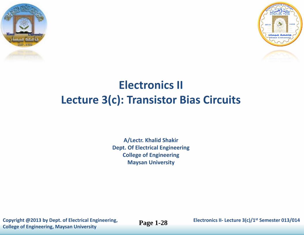
Voltage-Divider Bias- A method of biasing a transistor for linear operation using a
single-source resistive voltage divider.
- Earlier, a separate dc source, VBB, was used to bias the base-emitter
- junction because it could be varied independently of VCC,
& it helped to illustrate transistor operation.
- More practical bias method: use VCC as the single bias source.
- A dc bias voltage at the base of the transistor can be developed bya resistive voltage divider that consists of R1 & R2. VCC: the dccollector supply voltage
- 2 current paths are between point A & ground;(1) through R2, and (2) through the base-emitter junction of the
transistor & RE
- Generally, voltage-divider bias circuits are designed so that the base current is muchsmaller than the current (I2) through R2.For this case, the voltage-divider circuit is very straightforward to analyze because theloading effect of the base current can be ignored.
Page 2-28
Copyright @2013 by Dept. of Electrical Engineering, Electronics II- Lecture 3(c)/1st Semester 013/014College of Engineering, Maysan University
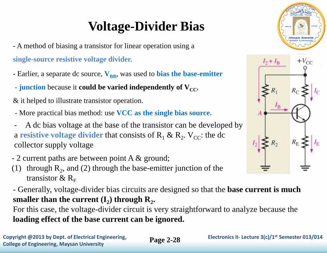
Stiff voltage divider: A voltage divider in which the base current is smallcompared to the current in R2 (the base voltage is relatively independent ofdifferent transistors & temperature effects).
Voltage-Divider Bias
Ideally, a voltage-divider circuit is stiff; where transistor does not appear asa significant load.To determine if the divider is stiff or not, then need to examine the dc inputresistance looking in at the base.
Page 3-28
Copyright @2013 by Dept. of Electrical Engineering, Electronics II- Lecture 3(c)/1st Semester 013/014College of Engineering, Maysan University
(1) DC Input Resistance at theTransistor Base
(2) Stability of Voltage-Divider Bias
(3) Voltage-Divider BiasedPNP Transistor
Loading-Effect of Voltage-Divider Bias
Page 4-28
Copyright @2013 by Dept. of Electrical Engineering, Electronics II- Lecture 3(c)/1st Semester 013/014College of Engineering, Maysan University
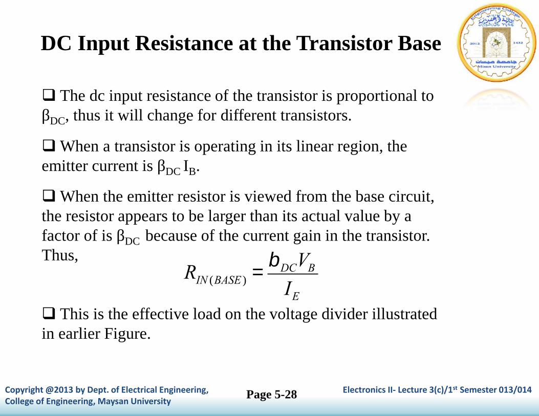
DC Input Resistance at the Transistor Base
The dc input resistance of the transistor is proportional toβDC, thus it will change for different transistors.
When a transistor is operating in its linear region, theemitter current is βDC IB.
When the emitter resistor is viewed from the base circuit,the resistor appears to be larger than its actual value by afactor of is βDC because of the current gain in the transistor.Thus,
This is the effective load on the voltage divider illustratedin earlier Figure.
RIN (BASE ) = bDCVBIE
Page 5-28
Copyright @2013 by Dept. of Electrical Engineering, Electronics II- Lecture 3(c)/1st Semester 013/014College of Engineering, Maysan University
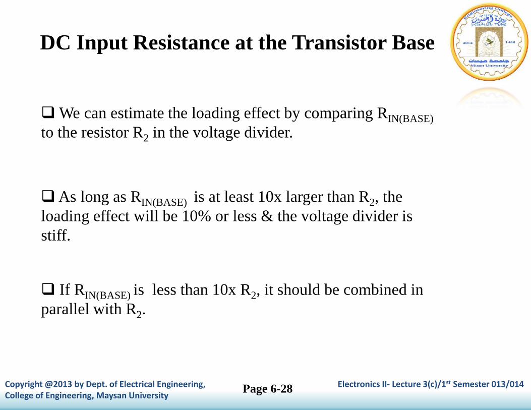
We can estimate the loading effect by comparing RIN(BASE)
to the resistor R2 in the voltage divider.
As long as RIN(BASE) is at least 10x larger than R2, theloading effect will be 10% or less & the voltage divider isstiff.
If RIN(BASE) is less than 10x R2, it should be combined inparallel with R2.
DC Input Resistance at the Transistor Base
Page 6-28
Copyright @2013 by Dept. of Electrical Engineering, Electronics II- Lecture 3(c)/1st Semester 013/014College of Engineering, Maysan University
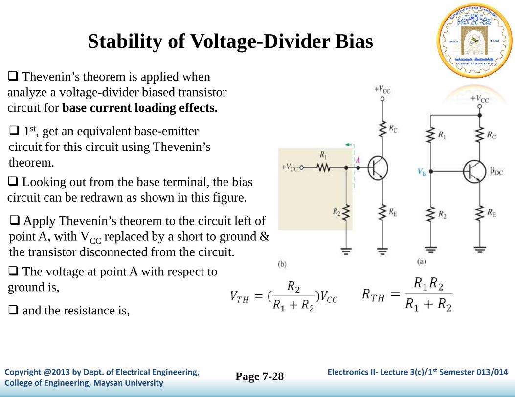
Thevenin’s theorem is applied whenanalyze a voltage-divider biased transistorcircuit for base current loading effects.
1st, get an equivalent base-emittercircuit for this circuit using Thevenin’stheorem.
Stability of Voltage-Divider Bias
Looking out from the base terminal, the biascircuit can be redrawn as shown in this figure.
Apply Thevenin’s theorem to the circuit left ofpoint A, with VCC replaced by a short to ground &the transistor disconnected from the circuit.
The voltage at point A with respect toground is,
and the resistance is,
Page 7-28
Copyright @2013 by Dept. of Electrical Engineering, Electronics II- Lecture 3(c)/1st Semester 013/014College of Engineering, Maysan University
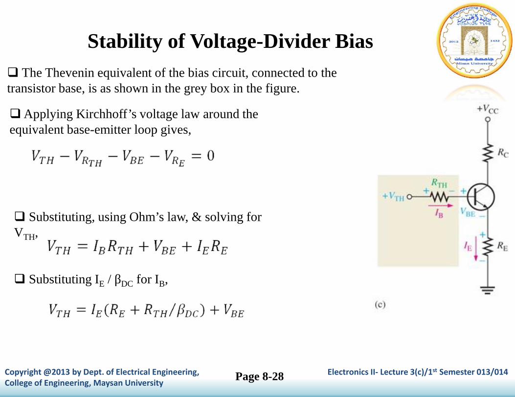
The Thevenin equivalent of the bias circuit, connected to thetransistor base, is as shown in the grey box in the figure.
Substituting, using Ohm’s law, & solving forVTH,
Substituting IE / βDC for IB,
Applying Kirchhoff’s voltage law around theequivalent base-emitter loop gives,
Stability of Voltage-Divider Bias
Page 8-28
Copyright @2013 by Dept. of Electrical Engineering, Electronics II- Lecture 3(c)/1st Semester 013/014College of Engineering, Maysan University
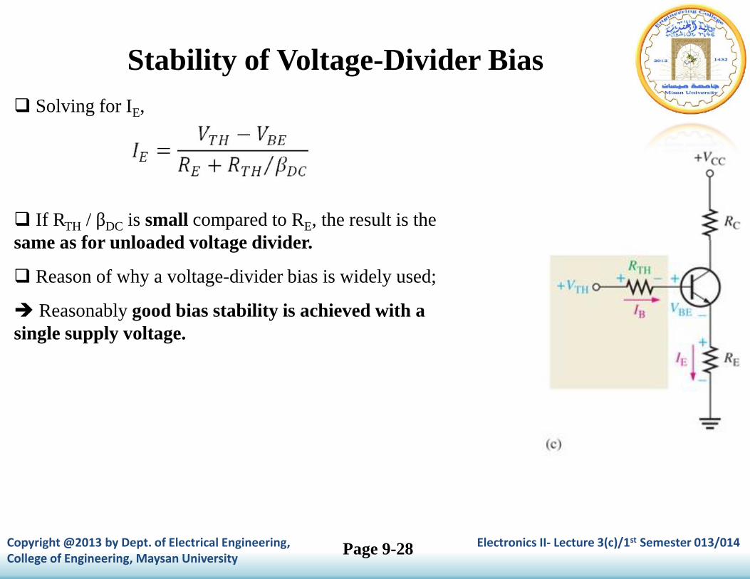
Stability of Voltage-Divider Bias Solving for IE,
If RTH / βDC is small compared to RE, the result is thesame as for unloaded voltage divider.
Reason of why a voltage-divider bias is widely used;
Reasonably good bias stability is achieved with asingle supply voltage.
Page 9-28
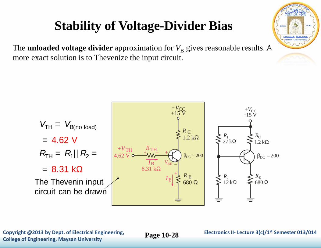
The unloaded voltage divider approximation for VB gives reasonable results. Amore exact solution is to Thevenize the input circuit.
+VCC
RCR1
RER2
βDC = 200
27 kW
12 kW
+15 V
680 W
1.2 kW
VTH = VB(no load)
= 4.62 VRTH = R1||R2 =
= 8.31 k WThe Thevenin inputcircuit can be drawn
R C
R TH
+VCC
R E
+V TH + –
IB
+
+
–
–IE
VBE
8.31 kW
680 W
1.2 kW
4.62 V
+15 V
βDC = 200
Copyright @2013 by Dept. of Electrical Engineering, Electronics II- Lecture 3(c)/1st Semester 013/014College of Engineering, Maysan University
Stability of Voltage-Divider Bias
Page 10-28
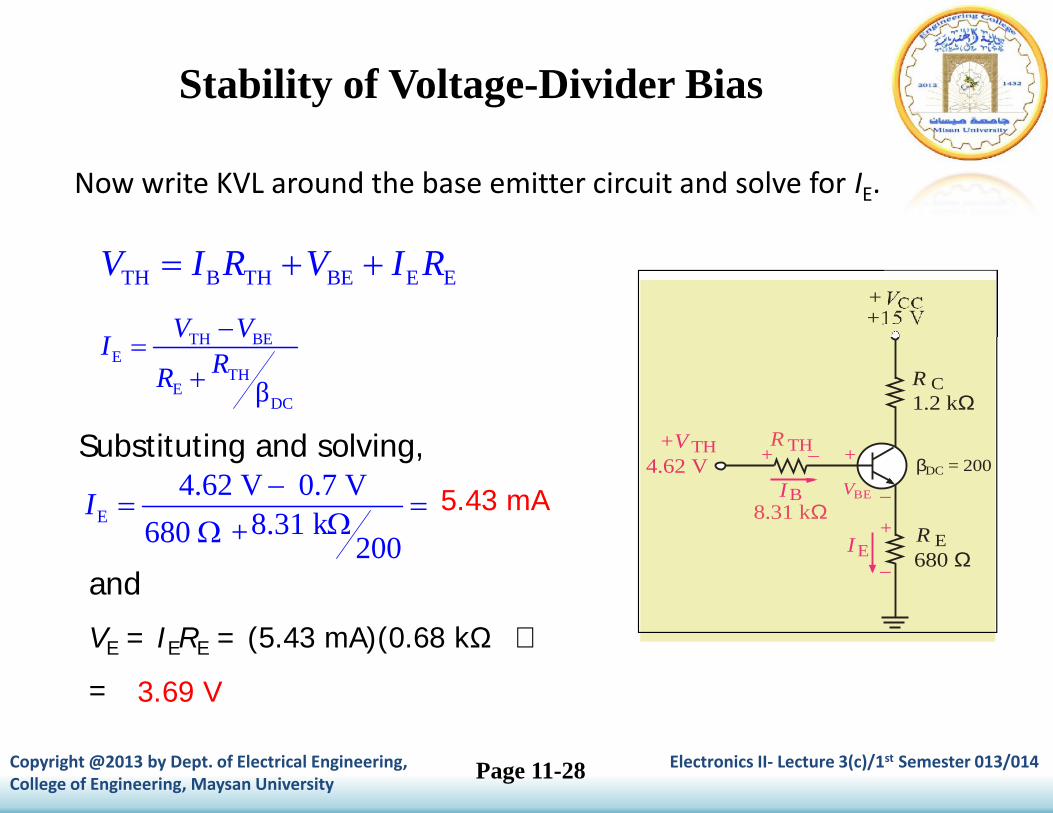
Now write KVL around the base emitter circuit and solve for IE.
R C
R TH
+VCC
R E
+V TH + –
IB
+
+
–
–IE
VBE
8.31 kW
680 W
1.2 kW
4.62 V
+15 V
βDC = 200
TH B TH BE E EV I R V I R
TH BEE
THE
DCβ
V VI
RR
Substituting and solving,
E
4.62 V 0.7 V8.31 k680 + 200
I
5.43 mA
and
VE = IERE = (5.43 mA)(0.68 k W )
=
Copyright @2013 by Dept. of Electrical Engineering, Electronics II- Lecture 3(c)/1st Semester 013/014College of Engineering, Maysan University
3.69 V
Stability of Voltage-Divider Bias
Page 11-28
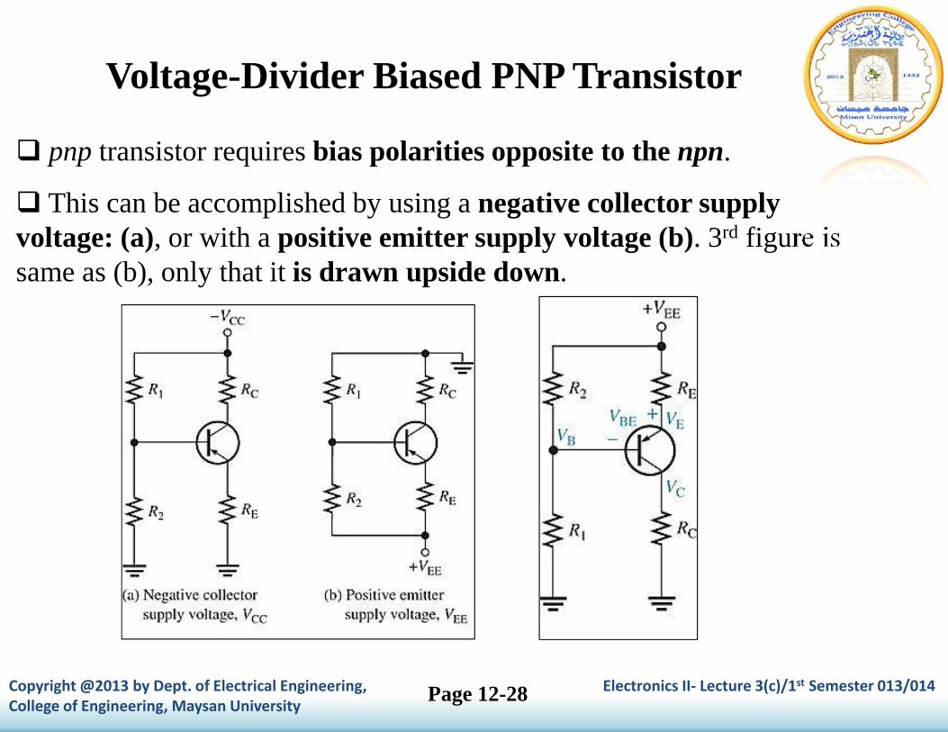
pnp transistor requires bias polarities opposite to the npn.
This can be accomplished by using a negative collector supplyvoltage: (a), or with a positive emitter supply voltage (b). 3rd figure issame as (b), only that it is drawn upside down.
Copyright @2013 by Dept. of Electrical Engineering, Electronics II- Lecture 3(c)/1st Semester 013/014College of Engineering, Maysan University
Voltage-Divider Biased PNP Transistor
Page 12-28
Copyright @2013 by Dept. of Electrical Engineering, Electronics II- Lecture 3(c)/1st Semester 013/014College of Engineering, Maysan University
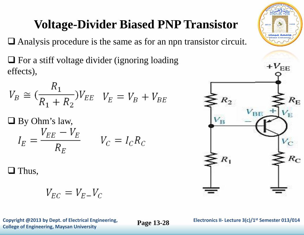
Analysis procedure is the same as for an npn transistor circuit.
For a stiff voltage divider (ignoring loadingeffects),
By Ohm’s law,
Thus,
Voltage-Divider Biased PNP Transistor
Page 13-28
Copyright @2013 by Dept. of Electrical Engineering, Electronics II- Lecture 3(c)/1st Semester 013/014College of Engineering, Maysan University
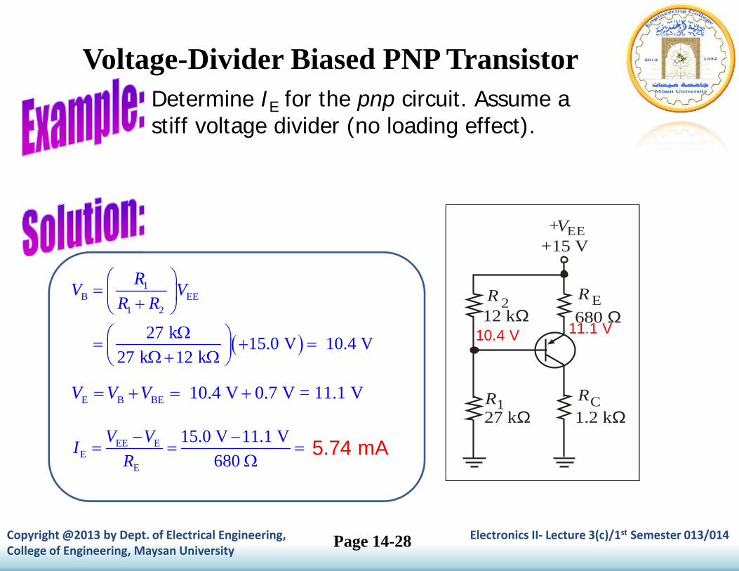
Determine IE for the pnp circuit. Assume astiff voltage divider (no loading effect).
1B EE
1 2
27 k15.0 V 10.4 V
27 k 12 k
RV V
R R
E B BE 10.4 V 0.7 V = 11.1 VV V V
EE EE
E
15.0 V 11.1 V
680
V VI
R
5.74 mA
+VEE
R 2
1R RC1.2 kW
R E680 W
27 kW
12 kW
+15 V
10.4 V 11.1 V
Voltage-Divider Biased PNP Transistor
Page 14-28
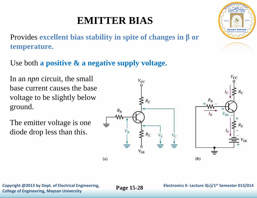
Provides excellent bias stability in spite of changes in β ortemperature.
Use both a positive & a negative supply voltage.
In an npn circuit, the smallbase current causes the basevoltage to be slightly belowground.
The emitter voltage is onediode drop less than this.
Copyright @2013 by Dept. of Electrical Engineering, Electronics II- Lecture 3(c)/1st Semester 013/014College of Engineering, Maysan University
EMITTER BIAS
Page 15-28
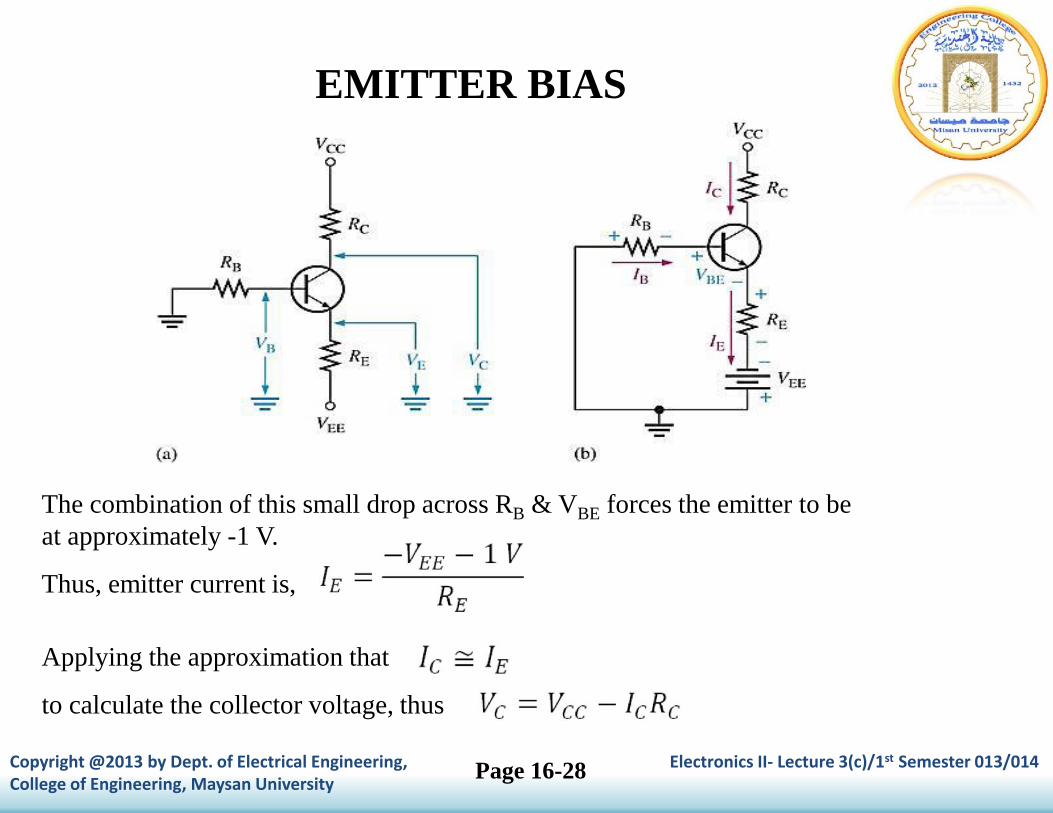
The combination of this small drop across RB & VBE forces the emitter to beat approximately -1 V.
Thus, emitter current is,
Copyright @2013 by Dept. of Electrical Engineering, Electronics II- Lecture 3(c)/1st Semester 013/014College of Engineering, Maysan University
EMITTER BIAS
Applying the approximation that
to calculate the collector voltage, thus
Page 16-28
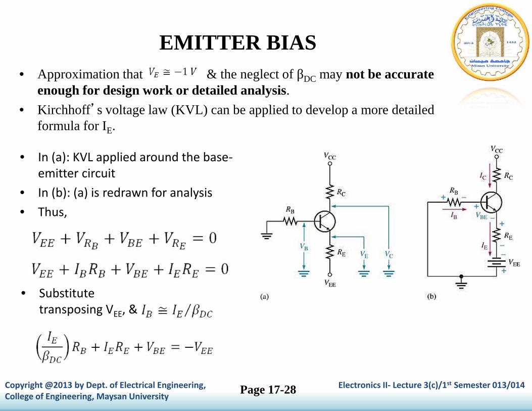
• Substitutetransposing VEE, &
• Approximation that & the neglect of βDC may not be accurateenough for design work or detailed analysis.
• Kirchhoff’s voltage law (KVL) can be applied to develop a more detailedformula for IE.
Copyright @2013 by Dept. of Electrical Engineering, Electronics II- Lecture 3(c)/1st Semester 013/014College of Engineering, Maysan University
• In (a): KVL applied around the base-emitter circuit
• In (b): (a) is redrawn for analysis• Thus,
EMITTER BIAS
Page 17-28
• Thus,
• Voltages with respect to ground are indicated by a single subscript.• Thus, the emitter voltage with respect to the ground is,
• The base voltage with respect to ground is,
• The collector with respect to the ground is,
Copyright @2013 by Dept. of Electrical Engineering, Electronics II- Lecture 3(c)/1st Semester 013/014College of Engineering, Maysan University
EMITTER BIAS
Page 18-28
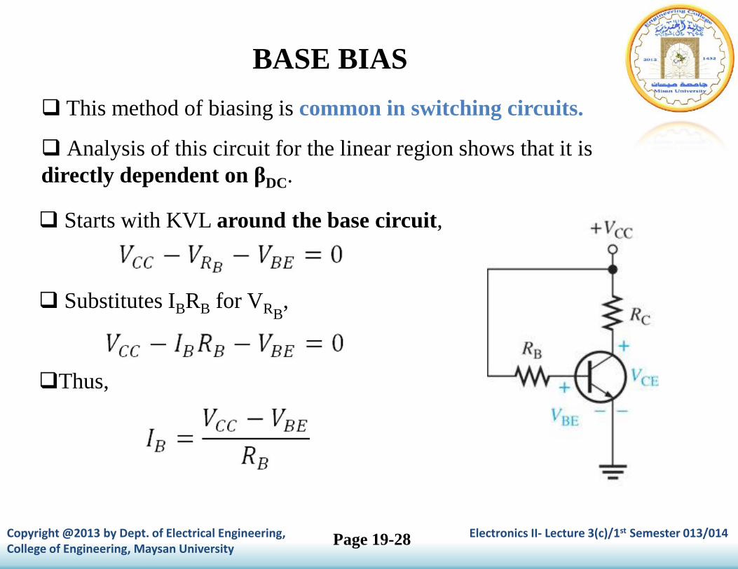
This method of biasing is common in switching circuits.
Analysis of this circuit for the linear region shows that it isdirectly dependent on βDC.
Starts with KVL around the base circuit,
Substitutes IBRB for VRB,
Thus,
Copyright @2013 by Dept. of Electrical Engineering, Electronics II- Lecture 3(c)/1st Semester 013/014College of Engineering, Maysan University
BASE BIAS
Page 19-28
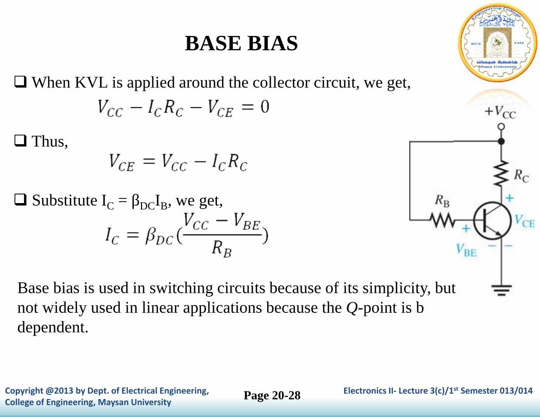
When KVL is applied around the collector circuit, we get,
Thus,
Substitute IC = βDCIB, we get,
Copyright @2013 by Dept. of Electrical Engineering, Electronics II- Lecture 3(c)/1st Semester 013/014College of Engineering, Maysan University
BASE BIAS
Base bias is used in switching circuits because of its simplicity, butnot widely used in linear applications because the Q-point is bdependent.
Page 20-28
Copyright @2013 by Dept. of Electrical Engineering, Electronics II- Lecture 3(c)/1st Semester 013/014College of Engineering, Maysan University
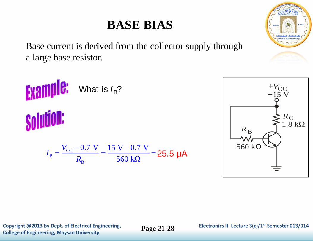
Base current is derived from the collector supply througha large base resistor.
What is IB?
CCB
B
0.7 V 15 V 0.7 V
560 k
VI
R
25.5 m A
RC
R B
+VCC
560 kW
+15 V
1.8 kW
BASE BIAS
Page 21-28
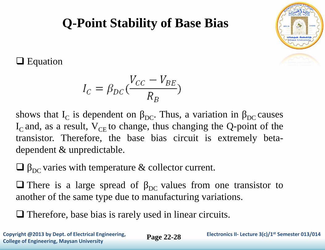
Q-Point Stability of Base Bias
Equation
shows that IC is dependent on βDC. Thus, a variation in βDC causesIC and, as a result, VCE to change, thus changing the Q-point of thetransistor. Therefore, the base bias circuit is extremely beta-dependent & unpredictable.
βDC varies with temperature & collector current.
There is a large spread of βDC values from one transistor toanother of the same type due to manufacturing variations.
Therefore, base bias is rarely used in linear circuits.
Copyright @2013 by Dept. of Electrical Engineering, Electronics II- Lecture 3(c)/1st Semester 013/014College of Engineering, Maysan University Page 22-28
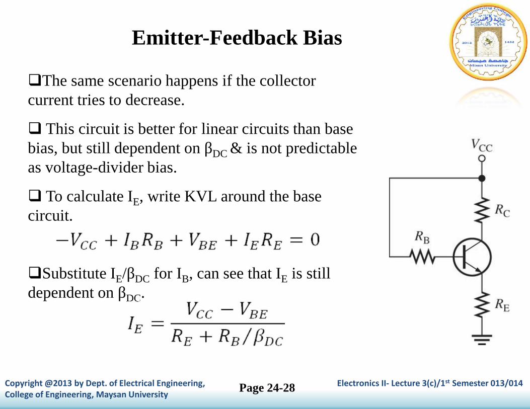
Emitter-Feedback Bias
Copyright @2013 by Dept. of Electrical Engineering, Electronics II- Lecture 3(c)/1st Semester 013/014College of Engineering, Maysan University
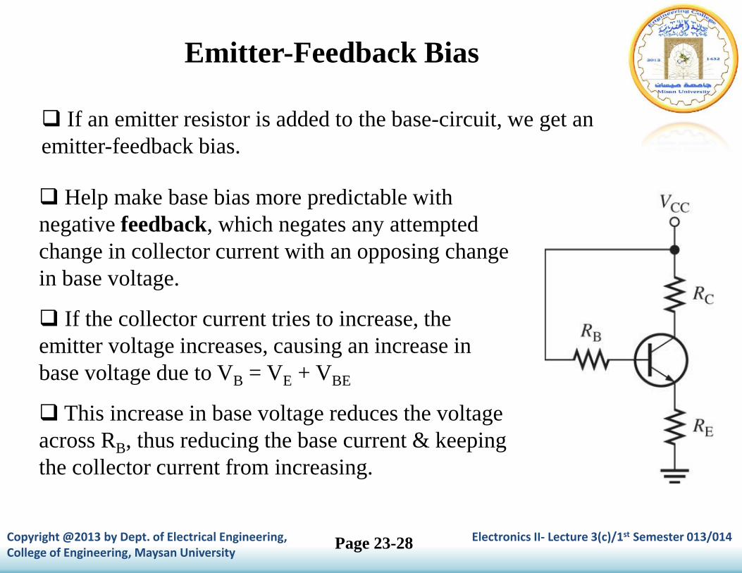
If an emitter resistor is added to the base-circuit, we get anemitter-feedback bias.
Help make base bias more predictable withnegative feedback, which negates any attemptedchange in collector current with an opposing changein base voltage.
If the collector current tries to increase, theemitter voltage increases, causing an increase inbase voltage due to VB = VE + VBE
This increase in base voltage reduces the voltageacross RB, thus reducing the base current & keepingthe collector current from increasing.
Page 23-28
Emitter-Feedback Bias
Copyright @2013 by Dept. of Electrical Engineering, Electronics II- Lecture 3(c)/1st Semester 013/014College of Engineering, Maysan University
The same scenario happens if the collectorcurrent tries to decrease.
This circuit is better for linear circuits than basebias, but still dependent on βDC & is not predictableas voltage-divider bias.
To calculate IE, write KVL around the basecircuit.
Substitute IE/βDC for IB, can see that IE is stilldependent on βDC.
Page 24-28
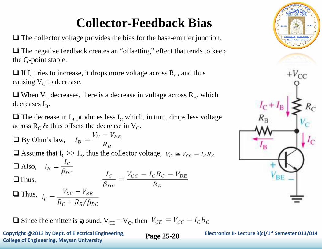
Collector-Feedback Bias
Copyright @2013 by Dept. of Electrical Engineering, Electronics II- Lecture 3(c)/1st Semester 013/014College of Engineering, Maysan University
The collector voltage provides the bias for the base-emitter junction.
The negative feedback creates an “offsetting” effect that tends to keepthe Q-point stable.
If IC tries to increase, it drops more voltage across RC, and thuscausing VC to decrease.
When VC decreases, there is a decrease in voltage across RB, whichdecreases IB.
The decrease in IB produces less IC which, in turn, drops less voltageacross RC & thus offsets the decrease in VC.
By Ohm’s law,
Assume that IC >> IB, thus the collector voltage,
Also,
Thus,
Thus,
Since the emitter is ground, VCE = VC, then
Page 25-28
Q-Point Stability Over Temperature
Copyright @2013 by Dept. of Electrical Engineering, Electronics II- Lecture 3(c)/1st Semester 013/014College of Engineering, Maysan University
Equation
shows that IC is dependent to some extent on βDC and VBE .
The dependency can be minimized by making RC >> RB/βDC &VCE >>VBE.
The collector-feedback bias is essentially eliminates the βDC &VBE dependency even if the stated conditions are met.
βDC varies directly with temperature, & VBE varies inversely withtemperature. As the temperature goes up in a collector-feedbackcircuit, βDC goes up & VBE goes down.
Page 26-28
Q-Point Stability Over Temperature
Copyright @2013 by Dept. of Electrical Engineering, Electronics II- Lecture 3(c)/1st Semester 013/014College of Engineering, Maysan University
The increase in βDC acts to increase IC. The decrease inVBE acts to increase IB which, in turn also acts to increaseIC. As IC tries to increase, the voltage drop across RC alsotries to increase. This tends to reduce the collector voltage& therefore the voltage across RB, thus reducing IB &offsetting the attempted increase in IC & the attempteddecrease in VC.
The result is that the collector-feedback circuitmaintains a relatively stable Q-point. The reverse actionoccurs when the temperature decreases.
Page 27-28
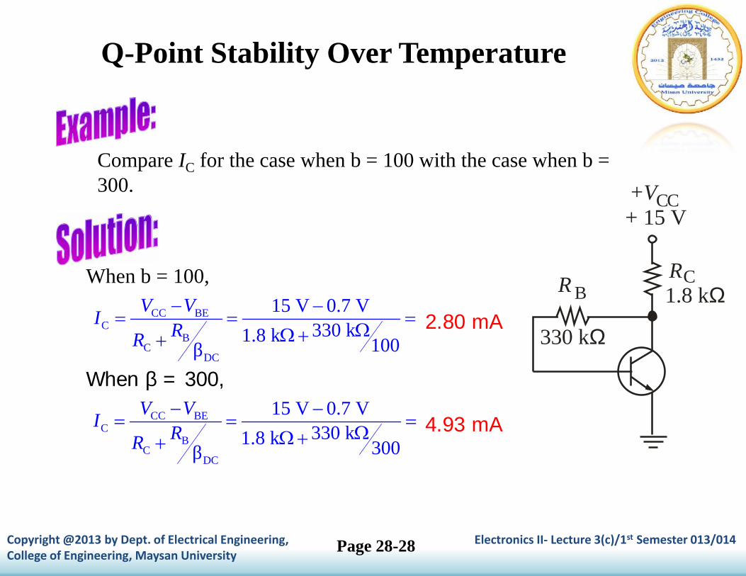
Q-Point Stability Over Temperature
Copyright @2013 by Dept. of Electrical Engineering, Electronics II- Lecture 3(c)/1st Semester 013/014College of Engineering, Maysan University
When b = 100,
CC BEC
BC
DC
15 V 0.7 V330 k1.8 k 100β
V VI
RR
+VCC
RCR B
330 kW
1.8 kW
+ 15 V
Compare IC for the case when b = 100 with the case when b =300.
2.80 mA
When b = 300,
CC BEC
BC
DC
15 V 0.7 V330 k1.8 k 300β
V VI
RR
4.93 mA
Page 28-28