Embed Size (px)
Citation preview

ZKZ 64717
07-08ISSN: 1863-5598
Electronics in Motion and Conversion July 2008

�
� P
�
�
Galvanic separation
Analog Applications JournalDESIGN BRIEF
By Jürgen Schneider
Introduction
With their wide input voltage range, the TPS40210
and TPS40211 PWM controllers are targeted for
isolated and non-isolated power converters used
in industrial, automotive, and battery-powered
applications. The full freedom in selecting the
power stage and its compensation—as well as the
advanced features, such as programmable soft
start, adjustable/synchronizable oscillator frequen-
cy and internal slope compensation—supports the
use of the devices in many applications. The basic
converter architecture can provide different power
levels by simply changing the power stage. While
the TPS40210 is designed for general-purpose
applications, the TPS40211 is tailored for driving
high-brightness LEDs.
Boost Converter Application
The devices and their basic configuration are
described in detail in Reference 1.
SEPIC Converter Application
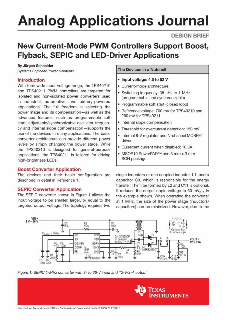
The SEPIC-converter shown in Figure 1 allows the
input voltage to be smaller, larger, or equal to the
targeted output voltage. The topology requires two
New Current-Mode PWM Controllers Support Boost,
Flyback, SEPIC and LED-Driver Applications
The Devices in a Nutshell
(programmable and synchronizable)
driver
single inductors or one coupled inductor, L1, and a
capacitor C9, which is responsible for the energy
transfer. The filter formed by L2 and C11 is optional.
p-p in

increased switching loss at this high frequency, a
-
frequency, converter efficiency was measured as
Flyback Converter ApplicationFigure 2 shows the TPS40210 controller configured
isolated supply. Key components include the trans-
-
sation (C19, C20 and R16), the output-voltage divider
)
regulation between the two secondary windings of
T1. When the negative output does not have a load,
R12 and D4 provide a basic load.
High-Brightness LED-Driver ApplicationDC/DC regulators are usually designed to provide a
constant-voltage output; however, LED applications
used to sense the LED current. The losses in R1 are
minimized with the TPS40211 because of its low
-
put overvoltage in the event of an LED-string open
circuit. The brightness can be programmed by alter-
ing R1, current injection into the FB pin, or by PWM
dimming. See Reference 1 for more information.
Reference
Related Device
Step-Down Converter
* Snubber for reduction of voltage stress and improved EMI
** Clamps negative output in case of heavily unmatched loads
*** Soft start and overshoot control
C O N T E N T S
Viewpoint The Next Big Thing is Blue Efficiency . . . . . . . . . . . . . . . . . . . . . . . . . . . . 4
Events . . . . . . . . . . . . . . . . . . . . . . . . . . . . . . . . . . . . . . . . . . . . . . . . . . . . 4
News . . . . . . . . . . . . . . . . . . . . . . . . . . . . . . . . . . . . . . . . . . . . . . . . . . . 6-9
Product of the MonthMulti-Output Programmable Power Manager Combines
Advanced Power Delivery with Digital Power Control . . . . . . . . . . . . 10-11
Guest EditorialHundred Dollar a BarrelBy Claus Petersen, Danfoss Silicon Power . . . . . . . . . . . . . . . . . . . . . . 12
MarketElectronics Industry Digest
By Aubrey Dunford, Europartners . . . . . . . . . . . . . . . . . . . . . . . . . . . . . . 14
Market DigitalPower is a Mainstrem Power Technology
By Douglas Bess, Editor, PowerPulse.NET . . . . . . . . . . . . . . . . . . . . 16-17
Cover Story 6500V SPT+ HiPak Modules. Higher power and SOA performance
By A. Kopta, M. Rahimo, U. Schlapbach, A. Baschnagel, ABB Semiconductor . . . . . . . . . . . . . . . . . . . . . . . . . . . . . . . . . . . . . . 18-21
IGBT600V Trench IGBTs Optimized for 20 kHz Operation
By Carl Blake and Wibawa Chou, International Rectifier . . . . . . . . . . 22-23
MOSFET Renewable Energy Application Efficency
By Dean Henderson, Segment Marketing Manager/Computing, Infineon Technologies North AmericaAnd Christian Wald,Senior Specialist, Regional Marketing Management, Infineon Technologies AG . . . . . . . . . . . . . . . . . . . . . . 24-25
Digital Power A Panoramic View of Applications and Challenges
By Steve Mappus, Systems Engineer,Fairchild Semiconductor, High Power Solutions, Bedford, NH . . . . . . . . . . . . . . . . . . . . . . . . . . 26-28
Digital Power Digital Power, Hope or Hype?
By Dr.– Ing. Artur Seibt, Vienna . . . . . . . . . . . . . . . . . . . . . . . . . . . . . 30-31
Power SupplyFlexible, Accurate & Efficient Power Solutions for
LED Backlighting Applications
By Steve Oliver, VP. V•I Chip Inc. (a Vicor company) . . . . . . . . . . . . . 32-35
CapacitorsSuper Capacitor Reference Design
By Thomas Delurio, Applications Manager, Advanced Analogic Technologies, Inc. . . . . . . . . . . . . . . . . . . . . . . . . 36-40
PCIM ImpressionsBlue Efficiency at the Next Level . . . . . . . . . . . . . . . . . . . . . . . . . . . . . . . 15
PCIM New Product Review . . . . . . . . . . . . . . . . . . . . . . . . . . . . . . . 40-44
New Products . . . . . . . . . . . . . . . . . . . . . . . . . . . . . . . . . . . . . . . . . . 45-48
Whatever you invent, imagine or develop, LEM’s transducers are at the heart of your power electronics applications from the very start.
LEM’s products, R&D, and people provide knowledge intensive solutions to keep up with your changing industry, allowing your visions to come to life.
www.lem.com
Already part of your vision.
LEM.

TThhee GGaalllleerryy
2 www.bodospower.comJuly 2008

Cure for the Uncommon Power SourceBarrel jacks are a simple and effective way of connecting portable electronics to an external power supply. But what happens when theuser plugs into a supply operating at the wrong voltage? Or whatabout when the supply is dirty and full of nasty voltage surges, as isoften the case when power is supplied from an automobile power jack?Raychem Circuit Protection PolyZen™ devices can help protect your DCpower ports by clamping excess voltages and smoothing inductivevoltage surges. The PolyZen device's unique polymer-protected precision Zener design can help cure these all-too-common powerproblems.
To learn more, visit www.circuitprotection.com/polyzen.
www.circuitprotection.comTyco Electronics Raychem GmbH Finsinger Feld 1 85521 Ottobrunn GermanyTel: +49 89 6089 386 Fax: +49 89 6089 394
© 2008 Tyco Electronics Corporation • www.tycoelectronics.com Raychem, PolyZen, TE Logo and Tyco Electronics are trademarks
Features• Overvoltage transient
suppression• Stable Vz vs fault current• Time delayed, overvoltage trip• Time delayed, reverse bias trip• Power handling on the order of
100 watts• Integrated device construction• RoHS compliant
Benefits• Stable Zener diode helps shield
downstream electronics from overvoltage and reverse bias
• Analog nature of trip eventsminimizes upstream inductivespikes
• Minimal heat sinking • Single component placement• Helps reduce warranty returns
& replacement costs
Applications• Cell Phones • Printers• PDAs • Scanners• MP3 Players • Hard Drives• DVD Players • Desk Phones• USB Hubs • PBX Phones• Media Players • Digital Cameras• Wireless Base Stations

No doubt about it - the industry is bringing
more specifics to Blue Efficiency. At PCIM
Europe, my podium discussion gave a repre-
sentative view from the electronic perspec-
tive. Key messages from the participants are
summarised and published in this edition. It
is always a pleasure to give an impulse for
new trends in the industry and I am happy to
see others following in my footsteps.
As expected, I planned something special for
the audience at the end of the open discus-
sion. Everyone enjoyed pulling the rope and
recognizing the winner. Three winners
received Marklin model train Starter Sets,
ten got Lego Locomotives, and eighty-seven
enjoyed pickles in a can - and every winner
got a bonus CD with all issues of Bodo’s
Power.
Inspiring children is important, as is develop-
ing their skills for an engineering profession.
We who are working in engineering must
give a high visibility to our jobs, and make it
attractive for young people to become engi-
neers. Creative toys and the skill to handle
them in construction are the forerunners for
solving problems in future generations.
Look for those who can get beyond the Nin-
tendo screens and just fighting a joystick for
satisfaction. The little engineers will be able
to assemble their train set and build scenery
from their imagination. What is needed is
continuous attention and support in all the
aspects of growing up. As long as I can
interest a few kids with such engineering
challenges, I will give away constructive
toys. As a child, a Marklin set from my older
brother was the seed that inspired me to
become an engineer. What worked for me
should still work for children today.
Creativity needs freedom and support - It
takes a while to see the results. A train set
can be a project to develop skills in long-
term activities and planning. Much of what is
needed to become an engineer is basic in
life – and to lifelong learning.
For all of you who missed traveling to
Nuremberg to see the innovations at PCIM,
the magazine has a summary of what was
showcased.
Now we are ready to take a break and relax.
It is summer and the beach is perfect these
days. For me it is easy, I just walk down the
hill and jump into the Baltic Sea.
Nevertheless, I will keep up with worki - my
magazine will reach you at the beginning of
each month, twelve times a year, and you
will be up to date. If you have subscribed,
you will be refreshed with twenty-four e-
news-letters during the year. And my publi-
cation is in the process of teaming up with
local publishers to carry news and articles
and content translated into local languages
to serve additional people with leading edge
information in their region.
My Green Power Tip for this month is:
Have your bikes ready for a weekend excur-
sion – your trip will achieve zero emissions!
I must push myself have to look into it as
well – but first I must visit my workshop and
fix all the little things to get the bike running.
I will report on my progress.
Regards
July 2008
The Next Big Thingis Blue Efficiency
Events
EPE – PEMC 2008
Poznan – Poland September 1-3
http://epe-pemc2008.put.poznan.pl
Husum WindEnergy 2008 Germany
September 9-13
http://www.husumwindenergy.com
Digital Power Forum 2008
San Francisco September 15-17
http://digitalpower.darnell.com
SEMICON Europe
Stuttgart Germany October 7-9
www.semiconeuropa.org
H2expo 2008
Hamburg, Germany October 22-23
http://h2expo.com
electronica 2008
Munich November 11-14
http://www.global-electronics.net
SPS/IPC/DRIVES 2008
Nuremberg November 25-27
http://www.mesago.de
V I E W P O I N T
4 www.bodospower.com
A MediaKatzbek 17a
D-24235 Laboe, Germany
Phone: +49 4343 42 17 90
Fax: +49 4343 42 17 89
www.bodospower.com
Publishing EditorBodo Arlt, [email protected]
Creative Direction & ProductionRepro Studio Peschke
Free Subscription to qualified readers
Bodo´s Power magazine
is available for the following
subscription charges:
Annual charge (12 issues) is 150 €
world wide
Single issue is 18 €
circulation
printrun
20000
Printing by:
Central-Druck Trost GmbH & Co
Heusenstamm, Germany
A Media and Bodos Power magazine
assume and hereby disclaim any
liability to any person for any loss or
damage by errors or omissions in the
material contained herein regardless of
whether such errors result from
negligence accident or any other cause
whatsoever.

Intersil – Switching Regulators for precise power delivery.©2007 Intersil Americas Inc. All rights reserved. The following are trademarks or services marks owned by Intersil Corporation or one of its subsidiaries, and may be registered in the USA and/or other countries: Intersil (and design) and i (and design).
High Performance Analog
Intersil Battery Authentication
We’re On It.
Intersil’s ISL9206 FlexiHash+TM
Engine delivers high-security battery authentication at a
low cost.
Intersil’s ISL9206 is an easy-to-use, robust,
and inexpensive battery authentication solution
for 1-cell Li-Ion/Li-Polymer or 3-cell NiMH
series battery packs.
Oscillator1-Wire Comm
Interface
16x8 OTPROM
FlexiHash+Engine
POR/2.5VRegulator
ControlRegister
32-bit pseudo-randomchallenge word
from host
8-bit authentication
code
32-bit HashFunction
64-bit Secret
32-bit HashFunction
FlexiHash+Engine
Patent pending FlexiHash+ engine
consists of four separate
programmable CRC calculators. Two
sets of 32-bit secret codes are used
for authentication code generation.
XSD single-wire host bus interface
communicates with all 8250-
compatible UARTs or a single GPIO
pin. Supports CRC on read data and
transfer bit-rate up to 23Kbps.
16 bytes of one-time programmable
ROM memory for storage of pack
information and ID, device
authentication secrets, device default
settings, and factory-programmed
trim parameters.
Go to www.intersil.com for samples, datasheets and support
ISL9206 Key Features:Challenge/response-based authentication scheme using 32-bit challenge code and 8-bit authentication code.
FlexiHash+ engine uses two sets of 32-bit secrets for authentication code generation.
16x8 one-time programmable ROM memory.
Additional programmable memory for storage.

N E W S
6 www.bodospower.comJuly 2008
Royal Philips Electron-
ics and its subsidiary,
Philips Healthcare,
recognized NEC LCD
Technologies, Ltd. for
its performance and
quality in 2007 with
two Philips “Partners for Growth” Global
Supplier Awards. These awards are a key
part of Philips’ strategic supplier relationship
management program, which brings together
Philips executives and representatives from
top suppliers to create a powerful network of
business partners to generate customer
value through shared goals, mutual
strengths and competencies. NEC LCD
Technologies supplies modules for patient
monitoring equipment to Royal Philips Elec-
tronics and Philips Healthcare.
Rob Green, president of NEC Electronics
Europe, said of receiving the award from
Philips on behalf of NEC LCD Technologies,
“NEC is proud to receive this prestigious
award. This award proves the success of our
strategy to develop and manufacture high-
quality liquid crystal display modules.
The awards were given to representatives
from NEC LCD Technologies’ sales and mar-
keting organizations in Europe and the
Americas.
www.eu.necel.com
Awards for Quality and Performance
Indium Corporation’s Indium8.9 Pb-Free No-
Clean Solder Paste was honored twice in
two weeks with leading electronics assembly
awards. Indium8.9 earned the VISION Award
at the APEX convention in Las Vegas, NV,
and just one week later, garnered the China
VISION award at NEPCON China in Shang-
hai, China. Sponsored by SMT Magazine,
and SMT China Magazine, the VISION
Awards honor the products and technologies
that have shaped the PCB manufacturing
industry over the past year.
Indium8.9 is a third-generation solder paste
that delivers more performance than any Pb-
free solder paste on the market, bringing
together the reliability of a Sn/Pb paste with
RoHS compliance.
Indium8.9 exhibits outstanding print-transfer
properties, especially with CSP, 0201, and
01005 components, with consistent print vol-
umes through apertures below the industry
recommended minimum area ratio of 0.66. A
robust reflow process window can accom-
modate high peak temperatures and long
soak profiles.
www.indium.com/big
Indium Corporation Wins Vision Awards
COMPEL 08 11th IEEE Workshop on Control
and Modeling for Power Electronics
(18-20 August 2008 ETH Zurich CH)
ESREF 19th European Symposium
"Reliability of Electron Devices, Failure
Physics and Analysis" including ECPE
Reliability Tutorial Session
(29 Sept - 2 Oct. 2008 Maastricht NL)
Automotive Power Electronics
(EC Projects) – Seminar
(7 – 8 October 2008, Stuttgart, D)
Advanced Cooling Techniques (1st day)
Power PCBs and Busbars (2nd day)
Workshop
(20 – 21 November 2008, Delft, NL)
Power Semiconductor
Devices & Technologies – Tutorial
(4 – 5 December 2008, Nuremberg, D)
www.ecpe.org
ECPE Seminars & Tutorial Programmes
7th International Conference and Trade Fair
on Hydrogen and Fuel Cell Technologies, 22
and 23 October 2008. Fossil fuels are run-
ning out. That is becoming more and more
evident with the current explosion in oil
prices and worldwide hunger for energy.
Action to mitigate climate change is just one
of the factors that is driving the efforts to
develop and secure alternatives, with hydro-
gen and fuel cells playing a key role. Along-
side the primary energy sources available in
the future, storage and conversion will
become increasingly important. The H2Expo
is a prominent forum for market-ready prod-
ucts and for concepts with future potential.
This 7th International Conference and Trade
Fair on Hydrogen and Fuel Cell Technolo-
gies at the CCH Congress Center Hamburg
on 22 and 23 October is a meeting place for
the expert community, for discussion of the
current state of developments. It will feature
presentations by scientists from Germany
and abroad, and reports from the industry on
innovative projects, showcasing their latest
products.
At the heart of this event is the scientific
conference, with a symposium on 22 Octo-
ber and three concurrent workshops on the
following day. Some 50 high-calibre speak-
ers from 11 countries are expected to partici-
pate. The main highlights this year are tech-
nical innovations in the individual fuel cell
types and their most promising applications,
in hydrogen production from renewable
energy sources, and in storage and infra-
structure.
The complete conference programme, indi-
cating the subjects and speakers at sympo-
sium and the workshops, is available at the
website:
www.h2expo.de
H2Expo 2008
The EnOcean Alliance and Texas Instruments announced that TI has
become a full member and participating company in the recently
established EnOcean Alliance. The Alliance was founded last month
to establish a global standard for sustainable buildings based upon
EnOcean´s revolutionary energy-harvesting wireless technology.
TI is a key semiconductor supplier to the EnOcean Alliance eco-sys-
tem, which includes innovators and industry leaders such as Masco,
Honeywell, Siemens, Osram Sylvania, Distech Controls, Omnio and
Thermokon. The EnOcean self-powered wireless technology has the
largest installation base in wireless building automation, with more
than 70 shipping customers, 300 available products and tens of thou-
sands of EnOcean-enabled buildings. Building professionals highly
value the interoperability across manufacturers and application pro-
files inherent to the EnOcean standard.
www.ti.com
www.enocean-alliance.org
TI Commits to EnOcean Standard for Energy-Harvesting

The 2SD315AI is a 2-channel driver forIGBTs up to 1700V (optionally up to3300V). Its gate current capability of±15A is optimized for IGBTs from 200Ato 1200A.
The 2SD315AI has been established on the market as an industrial standardfor the last four years. The driver has been tried and tested within hundreds of thousands of industrial and traction applications. The calculated MTBF to MIL Hdbk 217F is 10 million hours at 40°C. According to field data, the actualreliability is even higher. The operating temperature is -40°C...+85°C.
The driver is equipped with the award-winning CONCEPT SCALE driver chipset, consisting of the gate driverASIC IGD001 and the logic-to-driverinterface ASIC LDI001.
Driver stage for a gate current upto ±15A per channel, stabilized bylarge ceramic capacitors
Specially designed transformers forcreepage distances of 21mm between inputs and outputs orbetween the two channels. Insulat-ing materials to UL V-0. Partial dis-charge test according IEC270.
Isolated DC/DC power supply with3W per channel
Chipset Features
• Short-circuit protection• Supply undervoltage lockout• Direct or half-bridge mode• Dead-time generation• High dv/dt immunity up to 100kV/us• Transformer interface• Isolated status feedback• 5V...15V logic signals• Schmitt-trigger inputs• Switching frequency DC to >100kHz• Duty cycle 0...100%• Delay time typ. 325ns
CT-Concept Technology Ltd. is the technologyleader in the domain of intelligent driver com-ponents for MOS-gated power semiconductordevices and can look back on more than 15years of experience.
Key product families include plug-and-playdrivers and universal driver cores for medium-and high-voltage IGBTs, application-specificdriver boards and integrated driver circuits(ASICs).
By providing leading-edge solutions and expertprofessional services. CONCEPT is an essentialpartner to companies that design systems forpower conversion and motion. From custom-specific integrated circuit expertise to thedesign of megawatt-converters, CONCEPT pro-vides solutions to the toughest challenges con-fronting engineers who are pushing power tothe limits.
As an ideas factory, we set new standards withrespect to gate driving powers up to 15W perchannel, short transit times of less than 100ns,plug-and-play functionality and unmatched field-proven reliability.In recent years we have developed a series ofcustomized products which are unbeatable interms of today´s technological feasibility.
Our success is based on years of experience, ouroutstanding know-how as well as the will andmotivation of our employees to attain optimumlevels of performance and quality. For genuineinnovations, CONCEPT has won numerous tech-nology competitions and awards, e.g. the “SwissTechnology Award” for exceptional achievementsin the sector of research and technology, and the special prize from ABB Switzerland for thebest project in power electronics. This under-scores the company´s leadership in the sector ofpower electronics.
More information: www.IGBT-Driver.com/go/2SD315AI
CT-Concept Technologie AGRenferstrasse 152504 Biel-BienneSwitzerland
Tel +41-32-344 47 47Fax +41-32-344 47 40
Let experts drive yourpower devices
The Best-Selling 2-Channel IGBT Driver Core

N E W S
8 www.bodospower.comJuly 2008
Fairchild Semiconductor and Zilker Labs
have entered into an agreement to manufac-
ture and sell digital power products, includ-
ing point-of-load power devices, targeted at
the server, networking, graphics and high-
end desktop applications.
“We’re pleased to be able to expand our
industry-leading power management product
offering, particularly in the digital power area.
This partnership allows Fairchild to manufac-
ture and sell digital power products and
enhances our working knowledge of the digi-
tal power market and application space,
while promoting and driving its adoption.
Developing close relationships with our cus-
tomers, and understanding their challenges,
will allow us to develop and provide next
generation leading edge digital power prod-
ucts and solutions for a variety of applica-
tions in the power management market,”
said Bob Conrad, executive vice president of
Fairchild’s Mobile, Computing, Consumer
and Communications Product Group. “Zilker
Labs has developed an excellent reputation,
and we’re looking forward to working closely
with them.”
“Zilker Labs’ innovative Digital-DC™ technol-
ogy enables efficient, flexible, easy-to-use
digital power solutions for today’s embedded
communications and computing systems,”
said Bob Bridge, CEO of Zilker Labs. “We’re
excited about the partnership with Fairchild,
and we look forward to expanding both our
customer base and our product offering. The
partnership between Fairchild Semiconduc-
tor and Zilker Labs will allow increased prod-
uct support and supply continuity for OEMs
and power supply manufacturers using digi-
tal power control products.”
Zilker Labs’ Digital-DC ICs are highly-inte-
grated, high-performance digital power solu-
tions designed to be universal building
blocks that can be easily combined and
adapted to address a wide variety of com-
plex power system requirements.
www.zilkerlabs.com
www.fairchildsemi.com
Partnership to Provide Point-of-Load Digital Power Products
According to the World Fab Forecast report,
recently released by SEMI, spending on
worldwide fabs equipping is expected to
show declines of about 17 percent in 2008,
as more companies are forced
to postpone fab projects due to global eco-
nomic uncertainties. In 2009, however, the
group expects to see a rebound with double-
digit growth of over 12 percent.
Regions reflecting this trend most dramati-
cally include Southeast Asia and Taiwan,
who will likely experience declines of 40 per-
cent and 33 percent respectively this year,
but are expected to recover in 2009 with sig-
nificant positive growth of over 50 percent
and 80 percent respectively.
In the Americas, fab equipment spending is
expected to decline over the next two years,
while China and the Europe/Mideast are
expected to see growth both years. Spend-
ing in Japan and South Korea is projected to
remain slow, but should improve from nega-
tive double digits in 2008, to negative single
digits in 2009.
The biggest three spenders in 2008 for
equipping fabs are Samsung, Flash Alliance
and Intel. Though most companies are
investing in non-US fab opportunities, Sam-
sung is making significant investment into its
300mm megafabs in Austin, Texas, and Intel
continues to invest in its Arizona and New
Mexico fabs. In 2009, Rexchip, TSMC, UMC,
Promos and Hynix are expected to join Sam-
sung, Flash Alliance and Intel as key
spenders on fab equipping.
The SEMI World Fab Forecast provides high
level summaries and graphs; in-depth analy-
ses of capital expenditure, capacity, technol-
ogy and products, down to the detail of each
fab; and forecasts for the next 18 months.
These tools are invaluable for understanding
how 2009 will look, and learning more about
capex for construction projects, fab equip-
ping, technology level, and products.
www.semi.org/fabs
Strong Rebound in 2009 Says SEMI World Fab Forecast
Reinforcing its leadership in power manage-
ment and energy-efficient products, National
Semiconductor launched an initiative to help
customers create more energy-efficient sys-
tems that use less power, generate less
heat, have a smaller form factor and/or
longer battery life.
The trend towards energy conservation con-
tinues to grow worldwide. As market forces
drive higher user experience expectations
and the adoption of video streaming and
sharing, mobile broadband, and unlimited
storage capacity, the resources required to
power this trend are finite. Therefore,
enabling electronic systems to be more
energy efficient becomes imperative and is
especially important as the cost of energy
continues to rise.
At the system level, National helps cus-
tomers solve energy efficiency problems with
integrated circuits (ICs) from its PowerWise®
family of components as well as architecting
unique system solutions which it embeds in
silicon or licenses as intellectual property.
There are currently approximately 300 ICs in
National’s PowerWise family including ener-
gy-efficient power management, operational
amplifier, interface and data conversion
products.
www.national.com/powerwise
Solve System-Energy Challenges
Responding to the increasing momentum in
the electronics industry toward embedded
instrumentation, ASSET® InterTech, Inc.
announced it is positioning the company, its
products and its technologies to provide
open tools for embedded instrumentation in
design validation, test and debug applica-
tions.
Many of the established validation and test
technologies are inadequate or ineffective for
high-speed chips, I/O buses and systems.
Moreover, new chip geometries at 45
nanometers (nm) or smaller, as well as chip-
level packaging technologies like system-in-
package (SiP) are making validation, test
and debug very difficult, if not impossible
with traditional technologies. Building on its
long-established leadership in non-intrusive
boundary-scan structural test based on the
IEEE 1149.1 JTAG standard, ASSET has
significantly enhanced its ScanWorks® plat-
form over the last several years with embed-
ded instrumentation capabilities. According
to Glenn Woppman, president and CEO of
ASSET, the company will continue to lead in
JTAG structural test while developing inno-
vative and open embedded instrumentation
solutions.
www.asset-intertech.com
ASSET Aligns with Embedded Instrumentation
9www.bodospower.com July 2008
N E W S
International Development in the Offshore
Sector – a key subject at HUSUM WindEn-
ergy 2008
2008 and 2009 are expected to be boom
years in the offshore sector in Europe – with
planned commissioning of a total of 1507.5
MW on new installations coming online. The
United Kingdom alone is likely to account for
about 800 MW of this. Another milestone in
offshore energy production will be the com-
mercial launch of a number of wind turbines
of the 5 MW class. The European Wind
Energy Association (EWEA) predicts that, by
the end of 2010, a cumulative offshore
capacity of between 3000 and 4000 MW will
be operational off the coasts of Europe. Off-
shore is therefore a central theme at the
upcoming HUSUM WindEnergy 2008. This
premier fair of the wind energy sector will be
held in the Northern German coastal town of
Husum from 9 to 13 September. A large
number of international companies that
develop or already commercially operate
wind turbines specially developed for off-
shore application will exhibit their products,
projects and specialised services in Husum.
Presenting the latest technical and scientific
offshore wind advancements is also a main
theme at the HUSUM WindEnergy confer-
ence, which is an integral part of the fair.
The growth plans are promising – a Euro-
pean offshore goal of 40 000 MW by the
year 2020 was announced at the European
Offshore Wind Conference 2007 in Berlin.
The United Kingdom alone aims at 33 000
MW by 2020. Germany wants 25 000 MW
offshore wind power by 2030, sufficient to
cover 15% of its energy demand. Other
more moderate targets have been
announced by the Netherlands (6000 MW by
2020) and Sweden (2500 to 3000 MW by
2015). However, there could be bottlenecks
due to the scarcity of offshore wind turbines
and the restricted number of suppliers.
Outside Europe, countries like the USA and
China have announced plans to exploit their
offshore wind potential. According to a study
by the National Renewable Energy Labora-
tory (NREL), the offshore wind energy poten-
tial of the United States is more than 1 000
000 MW. By comparison, some 1100 MW
offshore capacity was installed in Europe by
the end of 2007, with Denmark and the UK
the two main markets. Supply of offshore
wind turbines is currently dominated by Ves-
tas (with a market share of about 60%) and
Siemens, both of them exhibitors at the
HUSUM WindEnergy 2008. At the beginning
of 2007, Vestas had to withdraw the V90-3
MW turbine from the market for technical
reasons, but has released the machine for
sale again from May 2008 onwards. At the
beginning of March, the Dutch developer
Evelop selected Vestas for supply of 110 tur-
bines (V90-3 MW) for its Belgian 330 MW
offshore project Belwind.
At the end of 2007 Siemens had offshore
turbines in operation with a total capacity of
434 MW, and projects with more than 1080
MW in new portfolio projects. In 2007 the
company for the first time installed 25 off-
shore turbines of the 3.6 MW category off
the British coast, at the Burbo Banks wind
farm. A UK project with 180 MW will be com-
pleted in 2008, and at least three more proj-
ects off the British and Danish coasts are
planned for 2009, with a combined capacity
of 400 MW.
Starting in 2008, a number of companies are
joining the offshore competition for commer-
cial use of 5 MW turbines. German compa-
nies REpower and Multibrid, also present in
Husum, each developed a 5 MW turbine for
offshore application. Each of these compa-
nies has been operating a prototype on
shore since the end of 2004, and the tur-
bines are now ready for series production.
Rapid international expansion in this sector
is expected following acquisition by the
French nuclear group Arreva of 51% of
Multibrid shares from the German project
developer Prokon Nord in 2007. This year, a
first batch of six Multibrid 5 MW turbines will
be installed in the German offshore test field
alpha ventus. REpower will install another
six turbines of this category there in 2009.
REpower was the first company in the world
to install 5 MW turbines in “real” offshore
operation – two of these are installed off the
Scottish coast, in a record water depth of 44
metres. Another 60 turbines are currently in
the initial project phase, for C-Power’s 300
MW Farshore wind farm off the Belgian
coast. A scaled-up 6 MW model will be
launched in the next few years. A joint ven-
ture with rotor blade manufacturer A&R
Rotec is to start in Bremerhaven in the near
future, under the project name of
PowerBlades, for production of 61.5 m off-
shore rotor blades developed by REpower.
Other companies are likewise active in the
offshore market. Converteam, for example,
is a key partner in the Dutch 4.7 MW Dar-
WinD offshore turbine project, supplying the
direct drive generator.
Nordex of Germany is operating a 2.5 MW
turbine in the port of Rostock, and will deliv-
er another 21 units for Baltic I, Germany’s
first commercial wind farm. This 52.5 MW
project is scheduled to go on-line in 2009.
Nordex decided to enter the offshore sector
on a step-by-step basis, starting with the
development of a new 3 to 5 MW turbine
with “offshore features”. A prototype is to be
built in 2010, and the 0 series by 2011/2.
WinWinD of Finland has installed three of its
3 MW Multibrid type wind turbines on artifi-
cial islands in the Kemi Ajos wind farm close
to the shore.
And finally, the Dutch company Blue H Tech-
nologies will provide information on its inno-
vative “floating” offshore wind turbine tech-
nology at the HUSUM WindEnergy 2008. A
prototype is currently being tested off the
Italian coast. The next (pre) series model will
feature a two-blade in-house modified 2.5
MW wind turbine.
HUSUM WindEnergy 2008 – the leading
international wind industry fair – has for the
first time been organised as a cooperation
venture between the Messe Husum and the
Hamburg Messe. From 9 to 13 September,
some 700 exhibitors from 35 countries will
present their products and services at the
Husum trade fair site, including the world’s
leading wind turbine manufacturers and their
equipment suppliers. This fair is dedicated to
the wind industry, and will be the internation-
al meeting point and forum for companies
and trade visitors for five days. Further
www.husumwindenergy.com
HUSUM WindEnergy 2008
TTI and Tyco Electronics have recently
entered an exclusive partnership on the dis-
tribution of connectors for the aerospace,
defence and marine market. The aim of the
agreement is to considerably strengthen the
presence of Tyco Electronics’ products in the
referred markets within the regions Europe,
Middle East and Africa.
TTI is already a preferred distributor of Tyco
Electronics with a strong global presence.
The company constantly proves that it
actively promotes Tyco Electronics’ product
portfolio, with a special emphasis being
made on demand creation and the genera-
tion of new business. Thanks to TTI’s com-
mitted Military, Aero and Space team
focussing on the markets in question, Tyco
Electronics expects a significant boost in
activities soon.
www.tycoelectronics.com/
www.ttieurope.com
Exclusive Partnership on Distribution

P R O D U C T O F T H E M O N T H
10 www.bodospower.comJuly 2008
Single-chip solution targets portable applica-
tions, maximizing design flexibility while
reducing system cost, size and development
time.
Summit Microelectronics has announced the
latest addition to the company’s family of
multi-output programmable power manager
ICs. The SMB119 is targeted at portable
consumer equipment and integrates seven
precision programmable regulators and a
wide range of digital power control functions.
This “one-chip” solution offers the highest
design flexibility in the industry, while reduc-
ing system solution size and cost.
Summit’s easy-to-use PC-based graphical
(GUI) development environment lets system
designers digitally program the entire multi-
ple output power supply and associated
power management functions with a few
clicks of a mouse. In high-volume produc-
tion Summit provides product that is pre-pro-
grammed with the customer’s “custom con-
figuration” at no extra cost. Compared to
inflexible conventional analog power ICs, the
SMB119 yields optimized power system
designs in significantly shorter development
time.
Features
The SMB119 incorporates three synchro-
nous step-down converters, two step-up
converters, one configurable step-up or step-
down converter, and one low-dropout (LDO)
linear regulator. Also included is a fully pro-
grammable system supervisor that monitors
all channels for under-voltage and over-volt-
age events. The user can select how the
SMB119 should react under abnormal condi-
tions (assertion of RESET output, power-
down in sequencing order or force shut-
down), thereby maximizing system reliability.
The power manager operates at a switching
frequency of 1MHz, allowing for space-sav-
ing system components. DC-DC Power con-
version efficiency of up to 95 percent
reduces thermal dissipation and improves
battery life in portable systems. Further
enhancing battery life, a shutdown mode
reduces current consumption to 0.1μA while
automatic PWM/PFM operation improves
light load efficiency. A PWM-override mode
is also available for noise sensitive RF or
audio applications. Short circuit current limit-
ing and thermal protection safety circuits are
also built-in to enhance reliability.
Programmability
The SMB119 provides Digital Power Man-
agement via an I2C interface and non-
volatile memory allowing the user to config-
ure power functions and parameters for each
channel: individual channel enabling/dis-
abling, power-up/down sequencing, power-
up slew rate control, static and dynamic out-
put voltage control (Dynamic Voltage Man-
agement). A broad range of intelligent power
system diagnostics and monitoring functions
can be easily accessed via the I2C serial
interface and digital status outputs. These
include input and output monitoring for
under/over-voltage/over-current (UV/OV/OC)
and integrated RESET control. Enhancing
flexibility even further, the device can be pro-
grammed during development and then used
in a "fixed" configuration, or it may be re-pro-
grammed in-system via the I2C interface.
Applications
The SMB119 is ideal for a wide range of
portable consumer electronics such as digital
still cameras/camcorders (DSC/DCC),
portable media players (MP3/MPEG4), GPS
terminals, portable medical equipment, per-
Multi-Output ProgrammablePower Manager Combines
Advanced Power Delivery withDigital Power Control
Summit Diagramm

sonal digital assistants (PDAs), as well as
the next generation of “smart” mobile
phones. The dynamic voltage management
feature is particularly useful in Xscale™ and
ARM™ CPU applications and where LED
backlight brightness control is desired.
The SMB119 operates directly from +2.7V to
+6.0V input making it ideal for 1-cell Li-Ion
(+3.0V to +4.2V) battery applications,
although line-powered applications are readi-
ly supported as well. The device has an
operating temperature range of +0°C to
+70°C or –40°C to +85°C and is available in
the 7mm x 7mm 48-pad QFN package that
is lead-free and RoHS-standard compliant.
Design Software/Hardware and Program-
mer for Prototype Development
To speed user product development, Summit
offers customers the SMB119EV companion
evaluation board and a graphical user inter-
face (GUI) software so designers can quickly
see the features and benefits and design a
prototype power supply with the SMB119.
This is a complete development tool that lets
designers easily manipulate the characteris-
tics of their systems. The SMB119EV design
kit includes menu-driven Microsoft Windows
(R) GUI software to automate programming
tasks and also includes all necessary hard-
ware to interface to the USB port of a laptop
or PC.
Once a user completes design and prototyp-
ing, the SMB119EV automatically generates
a HEX data file that can be transmitted to
Summit for review and approval. Summit
then assigns a unique customer identifica-
tion code to the HEX file and programs the
customer’s production devices prior to final
electrical test operations. This ensures that
the device will operate properly in the end
application. The design kit software can be
downloaded from Summit’s website.
A reference design that utilizes the SMB119,
7-level programmable power manager, and
the SMB137, switch-mode charger with Cur-
rentPath™ control, is also available for
accelerating product development for a com-
plete portable system design.
About Summit Microelectronics
Summit Microelectronics is the leader in flex-
ible, highly integrated power management
solutions combining precision power regula-
tion with sophisticated digital control in a sin-
gle chip. The Company’s devices are found
in a variety of consumer, communications
and computing applications.
Summit’s unique programmable, non-volatile
mixed-signal IC technology combined with a
convenient GUI development environment
allows for unparalleled functional and para-
metric flexibility in power supply design. This
flexibility applied to common problems such
as dynamic voltage/current control and intel-
ligent battery charging, allows for significant
system performance improvement while real-
izing drastic reductions in design effort.
Digital programmability enables high integra-
tion and system flexibility in a single chip -
impossible with conventional “hard-wired”
analog power ICs. Additionally, this integra-
tion reduces the bill-of-materials yielding the
lowest total system cost and size. Summit
solutions address the biggest challenges
facing OEM developers today: increasing
system functionality, performance and com-
plexity accompanied by shrinking develop-
ment time cycles.
www.summitmicro.com
P R O D U C T O F T H E M O N T H
MAKING MODERN LIVING POSSIBLE
Simplify your design!
Danfoss Silicon Power GmbH • Heinrich-Hertz-Straße 2 • D-24837 Schleswig, Germany • Tel.: +49 4621 9512-0 • Fax: +49 4621 9512-310
E-mail: [email protected] • http://siliconpower.danfoss.com
E0 to E3 size Short and long pins Flexible pin-outIGBT’s and MOSFET’s from world class manufacturers Low and high voltage
For industry, transportation and automotive
We design and manufacture to your needs.
99
36

12 www.bodospower.comJuly 2008
Earlier this year, the world was shocked
when crude oil prices exceeded the
$100 per barrel mark. Now, oil commodi-
ty experts are attempting to prepare us
for the next shock of $200 per barrel
crude oil.
Most people worry about rising energy
prices. After all, nobody wants to pay
increased prices for electricity, petrol or
heating. However, there is an up-side.
Whether we like it or not, we all know
that we must do something drastic to
reduce our dependence on fossil fuels.
Along with the benefits of CO2 reduction
and improved air quality, we can also
reap the economic benefits of substitut-
ing fossil fuels with renewable energy
sources.
For those of us in the power electronics
community, we have our work cut out for
us! Photovoltaic and wind power conver-
sion equipment and hybrid electric vehi-
cles, as a matter of fact, most renewable
energy sources, use power electronics
as “the” enabling technology.
This will come as no surprise to most readers of “Bodo’s Power”
magazine, but we tend to keep our growing need for talent as a big
secret within our relatively small community. Our secrecy complicates
any efforts to recruit new talent to our cause and meet the power
electronics industry’s great unfulfilled need for power electronics pro-
fessionals.
I want to make the point that we in the power electronics industry
must cultivate excitement and awareness about our profession in the
world. If we want to recruit enough of the best minds, we must work
to attract young people to our industry during the time in their lives
when they are making important decisions about their education.
Our industry is full of exciting success
stories that will attract our future col-
leagues. Wind turbines in Northern Ger-
many and Denmark that today account
for more than 20% of the total electricity
consumption work only in an efficient
manner due to advanced power
electronics components. The same can
be said for photovoltaic energy genera-
tion that requires efficient power elec-
tronics components in order to feed the
power grid.
Whether used to accelerate an electric
motor or regenerate braking power,
power electronics is the enabling tech-
nology for hybrid electric vehicles. More
recently, our situation receives good
publicity from Formula 1 Racing. Formu-
la 1 teams will soon be required to race
hybrid electric cars in order to compete
in this sport.
A very pleasant surprise it was when
someone introduced me to a little “Pixi”
booklet at the recent PCIM 2008 exhibi-
tion. Phoenix Contact sponsors this booklet that tells the story of an
electrical engineer as seen through the eyes of a very young girl.
Phoenix Contact is taking positive action to raise the awareness of
the engineering profession in a young target group. Through Danfoss
Universe (http://www.danfossuniverse.com/), Danfoss introduces
young people to the engineering profession. I encourage everyone
else in our profession to follow these good examples and do even
more!
http://siliconpower.danfoss.com
G U E S T E D I T O R I A L
Two Hundred Dollar a BarrelBy Claus Petersen, CEO Danfoss Silicon Power
PCIM review by VideoJust go to Darnell PowerPulse and watch what industry presented!
http://www.powerpulse.net/conferenceVideo.php
You find more videos from industry about PCIM produced by ICC media!http://ece-news.stc-d.de/pcimvideos/pcim/pcim08videos.html


14 www.bodospower.comJuly 2008
M A R K E T
ELECTRONICS INDUSTRY DIGESTBy Aubrey Dunford, Europartners
GENERAL
Worldwide revenue
for photovoltaic cells
is projected to
increase to as much
as $22.1 billion in
2012, up from $9.6
billion in 2007, so
iSuppli. By 2020,
about 50,000
Megawatts worth of PV systems (MWp) will
be installed annually, up by a factor of nearly
20 times from 2,538 MWp in 2007. But pro-
duction capacity limitations are constraining
polysilicon supply, causing PV suppliers to
realign their strategies and to seek alterna-
tive raw materials. The silicon shortage also
is driving the advancement of thin-film tech-
nologies that can act as the raw material for
PV cells. This will cause the revenue market
share of thin-film technologies to rise to 20
percent of the total PV market in 2010, up
from 5 percent in 2007.
SEMICONDUCTORS
The capacity utilization of semiconductor-
manufacturing plants worldwide edged up
0.1 percentage point from the previous quar-
ter to 90.5 percent, marking the fifth straight
quarter of rise, so SICAS. Actual wafer-starts
rose sequentially by 1.9 percent to 1.950
million per week in 8 inch equivalent wafers.
The utilization of advanced facilities that
make chips with circuits of less than 80 nm
came to 96.7 percent.
Freescale has informed workers at its plant
in East Kilbride, Scotland, that it was unable
to sell the fab and that it may be closed.
1,000 are employed at the site, with approxi-
mately 750 directly involved in manufactur-
ing. Freescale is also to close down its
design center in Cork, Ireland, with the loss
of 47 design engineering jobs, so Irish media
reports.
DIGEST – FORM
ON Semiconductor has announced plans to
close its two wafer manufacturing facilities
located in Piestany, Slovakia, and transfer
the production lines to other company-
owned facilities.
Texas Instruments has acquired Ireland-
based Commergy Technologies, a power
supply referenceb design provider that spe-
cializes in energy efficient and compact
architectures. The acquisition allows TI to
broaden its focus on improving energy effi-
ciency in endequipment designs, especially
in the areas of AC adapters and high-power-
density computing and server systems.
IXYS, a Silicon Valley power semiconductor
company, has made a proposal to acquire all
the outstanding shares of ZiLOG common
stock for per share consideration of $4.50, to
be paid in cash and stock. ZiLOG's micro-
controller semiconductor devices will com-
plement IXYS's IC business, so IXYS.
OPTOELECTRONICS
Large-sized LCD panel shipments in 2008
are projected to rise to 458.9 million units,
up 17.7 percent from 389.8 million in 2007,
so iSuppli.
Germany is a leading European market for
flat panel displays. In 2007, nearly 4.5 mil-
lion units of LCD and plasma television sets
were sold in Germany. Displaybank forecast
that the LED market would grow from US
$2,6B in 2006 to US$8.4B in 2011 with a
yearly average growth rate of 18 percent.
PASSIVE COMPONENTS
Germany’s PCB market revenue for Febru-
ary 2008 registered a 12.8 percent growth
compared with the same period last year,
albeit lower revenue compared with the pre-
vious month, so the ZVEI. During the first
two months of the year, total orders were 9
percent higher compared with the same peri-
od last year. Book-to-bill ratio, meanwhile,
stands at 1.06.
OTHER COMPONENTS
ANSYS has signed a definitive agreement to
acquire Ansoft for a purchase price of
approximately $ 832 M. The complementary
business combination of ANSYS and Ansoft
will create a provider of simulation capabili-
ties, with combined trailing 12-month rev-
enues of $ 485 M.
EMS PROVIDERS
Flextronics has completed its previously
announced acquisition of the FRIWO Mobile
Power (FMP) business unit of CEAG, a glob-
al market leader for power supplies and
chargers for mobile telephones. FMP is now
part of Flextronics' power supply division.
The acquisition will add approximately
18,000 employees and 700,000 square feet
of manufacturing capacity in China.
DISTRIBUTION
Future Electronics EMEA have been recog-
nized as the International Rectifier distributor
of the year for 2007. Avago Technologies
has also chosen Future Electronics for its
performance excellence in resale growth
across Europe. This was followed by Future
Germany's recognition by Avago for best
country performance for 2007. Future has 41
sales offices in 26 counties in the Europe,
Middle East and Africa region.
This is the comprehensive power related
extract from the « Electronics IndustryDigest
», the successor of The Lennox Report. For
a full subscription of the report contact:
[email protected] or by fax 44/1494
563503.
www.europartners.eu.com

P C I M I M P R E S S I O N S
Pull the rope.
We had 100 winners. Three walked away with a Marklin Starter Set.
Ten had a Lego Locomotive and all the others had a pickle in a can.
All of the winners walked away with the CD with all of the magazine
issues as pdfs.
It was so good to see so many happy people.
Bodo’s Podium at the PCIM show had put the mile stones down to
look into the future.
Just a few impressions and statements from experts.
Ecodesign and Efficiency
By Alfred Hesener, Director Applications&Marketing,
Fairchild Semiconductor EU
Ecodesign impacts: High efficiency (>94%), low standby power
(210mW), lowest component count and space requirements.
Blue Efficiency
By Dr. Martin Schulz AIM PMD ID TM Infineon
Energy Efficiency: the useful work per quantity of energy
Electrical Efficiency: useful power output per electrical power con-
sumed
Decreasing Computing Power Consumption
By Adam Latham, Intersil
The efficiency of the phase dropping/adding MOSFET drivers based
on LSI protocol data provides significant power savings. However, it
is not as efficient as the discrete circuitry solution that dynamically
adjusts based on current levels
The Next Level for Design
By Eric Persson, Executive Director, Global FAE,
International Rectifier
New Products targeted specifically at renewable energy inverters
(distributed solar arrays)
Blue Efficiency the Design
By Werner Berns, Technical Support Manager &
University Collaboration Europe National Semi-
conductor
PowerWise® Adaptive Voltage Scaling (AVS)
technology reduces energy consumption by
64% over other solutions for digital systems
Go Blue with TI
By François Malléus, EMEA Power Solutions & Services
Texas Instruments
Supporting renewable energy sources :
Generation: Letting nature work for us
Distribution: Smart metering and grid management
Smart appliances
Blue Efficiency at the Next Level

Recent news demonstrates that digital power conversion is no longer
just an emerging technology - digital power has entered the main-
stream. Some of the more interesting developments include: Infi-
neon’s purchase of Primarion, Fairchild’s second-source agreement
with Zilker Labs, Ericsson’s announcement of a digitally-controlled
MicroTCA power module, among others.
Infineon’s perspective on digital power can be seen in the following
statement made at the time of the Primarion acquisition: “Infineon will
now be positioned to set the benchmark in system density, efficiency
and control by combining the performance of Primarion’s digitally
controlled power-management devices with Infineon’s leading power
semiconductors portfolio,” said Peter Bauer, Member of the Manage-
ment Board and Head of Infineon’s Automotive, Industrial and Multi-
market Business Group.
“The addition of Primarion helps accelerate our access to the poten-
tial growth in the digital power segment by providing advanced sys-
tem solutions for our customers. This investment is also a great com-
plement to our power management activities based out of Villach in
Austria,” Bauer concluded.
Fairchild is similarly enthusiastic about digital power. Although
Fairchild is not a newcomer (the company has had a digital power
development effort underway for some time), Bob Conrad, Fairchild’s
Executive Vice President of the Mobile, Computing, Consumer and
Communications Product Group stated, “This partnership allows
Fairchild to manufacture and sell digital power products and
enhances our working knowledge of the digital power market and
application space, while promoting and driving its adoption.”
“Developing close relationships with our customers, and understand-
ing their challenges, will allow us to develop and provide next-gener-
ation, leading edge digital power products and solutions for a variety
of applications in the power management market,” Conrad predicted.
More recently, Zilker introduced what it describes as the industry’s
most accurate dc-dc power controller for meeting the ever-increasing
voltage regulation accuracy requirements of today’s high-perform-
ance embedded processors and ASICs. The ZL2004-01 uses Zilker
Labs’ Digital-DC technology to provide ±0.2% dc output regulation,
which is said to enable the most integrated and cost-effective solution
for delivering accurate power to sensitive devices, regardless of the
use of analog or digital techniques.
The ZL2004-01 interfaces with external drivers and MOSFETs, pro-
viding a flexible controller that can be implemented using a wide vari-
ety of power train components. The device also supports active cur-
rent sharing, allowing up to 8 devices in parallel to supply load cur-
rent requirements in excess of 100A.
The mainstreaming of digital power is also evident in the recent
announcement of a MicroTCA power converter by Ericsson Power
Modules. The digital control of the dc-dc converter that is embedded
within the module is described as being truly unique to Ericsson and
as providing cutting edge performance in terms of the level of control
available, and efficiency.
The power module was initially announced during 2007 as an evalua-
tive level product intended for interoperability testing. The results
from numerous interoperability workshops together with MicroTCA
component suppliers and system integrators have been incorporated
into the product, now called BMR 911 483/1. Two features that have
been added are a USB interface that is accessible to the user via the
faceplate, and redundant operation of payload and management
power.
MicroTCA is for use in many different types of applications and kinds
of Information and Communication Technology (ICT) equipment.
Some of the most suitable ones will most likely be edge and access
equipment. In addition to applications in the communications industry,
this power module is also suitable for applications targeting enter-
prise, military, medical and industrial markets.
In a related action, Verizon has established its own energy-consump-
tion standards and an associated measurement process for new
telecommunications-related equipment. The standards will be applied
to certain broadband, video, data-center, network and customer-
premises equipment purchased after January 1, 2009.
The target provided to the manufacturers of such equipment is 20%
greater efficiency than today’s gear. While not specifically calling for
digital power techniques, achievement of this level of efficiency is
often accomplished with a digital control loop.
“This is similar to a consumer buying appliances according to the
standardized ENERGY STAR® efficiency levels,” said Mark Wegleit-
ner, Senior Vice President-Corporate Network and Technology. “How-
ever, in most cases, an ENERGY STAR-type rating system did not
exist for the equipment we buy, so we set up our own standards and
measurement process to create an effective program. We want to
reduce our energy usage and do our part to improve the environ-
ment. We’re proud to be leading the industry with this initial, impor-
tant step, and invite others to use these standards so the cumulative
effect is increased.”
Verizon established a series of Telecommunications Equipment Ener-
gy Efficiency Ratings based on formulas that test the consumption of
equipment in various operating conditions and settings. Test data are
entered into formulas developed for each type of equipment, which
will indicate whether or not they achieve the target rating.
Equipment to be tested and rated includes optical and video trans-
port systems, switches and routers, DSLAM high-speed internet
equipment and optical line termination gear, as well as switching
power systems, data center servers and power adapters that operate
customer equipment.
M A R K E T
16 www.bodospower.comJuly 2008
Digital Power is a MainstreamPower Technology
By Douglas Bess, Editor, PowerPulse.Net

The requirements incorporate new applications of existing method-
ologies as outlined in SPECpower_ssj2008™ and the Energy Star
programs, combined with what are described as some innovative
Verizon-led concepts and methods of measurement. The concepts
and measurement methods have been submitted for consideration
by appropriate standards bodies, such as ATIS’ Network Interface,
Power and Protection Committee (NIPP).
CHiL Semiconductor, a developer of mixed-signal power manage-
ment ICs for a wide variety of computing devices, announced the
successful completion of its second major round of venture capital
financing, securing $16.7 million. Silicon Valley investor Panorama
Capital led the new round and joined the initial investor group of
Flybridge Capital Partners, Highland Capital, and IdSoft Capital.
The CHiL controller architecture is said to use mixed-signal technol-
ogy to optimize performance, increase power efficiency and
streamline the design. CHiL’s use of digital power techniques with
non-linear control is said to result in a very high bandwidth solution,
and to deliver a fast transient response for high performance
servers, computers and other systems requiring high efficiency
solutions. By efficiently using digital technology, CHiL claims that its
devices integrate a number of differentiating features such as moni-
toring and control capabilities with real-time response.
“As the world moves toward computing solutions that are environ-
mentally friendly, curtailing power consumption is the key” noted
Ram Sudireddy, Chief Executive Officer, CHiL. “We are implement-
ing our product roadmap for more efficient solutions, which ensures
that our customers can maximize their design investments with an
ongoing stream of new products with innovative technology and
features. This new round of funding will extend our global reach to
system and board designers in key markets in Asia Pacific and
North America.”
The mainstream nature of digital power is evident beyond the
news. It can be seen in the industry’s response to the fifth annual
Digital Power Forum. This year’s event has broadened to include
all aspects of embedded system powering, not just digital power
management and digital power conversion.
In response to industry demand, the 2008 Digital Power Forum
(DPF ’08), has added a new track of papers on Advanced Compo-
nents to the two existing tracks on Power Conversion and Mission
Critical Facilities. Papers will be presented on planar magnetics,
advanced thermal solutions, new semiconductor devices, including
Silicon Carbide, in addition to detailed discussions of power man-
agement, energy efficiency and, of course, digital power technolo-
gies.
“Our expanded content is a reflection of the fact that digital power
has rapidly become a mainstream power technology for embedded
systems,” stated Jeff Shepard, President of Darnell Group. “Two
years ago, if an engineer was considering using digital power tech-
nology, they had better have had a good reason. Today, an expla-
nation is necessary if digital power is not being considered,” Shep-
ard observed.
http://digitalpower.darnell.com
www.PowerPulse.net
www.bodospower.com
flowPACK 2 3rd gen up to 150A at 1200V
High Power Sixpacks forMotor Drives
IGBT4 technology for lowsaturation losses and improved EMC behavior
Low inductance layout and compact design
High power flow 2 housing
�
�
�
Power Modules
www.vincotech.com
NEW
Main Features
P68X series
18 www.bodospower.comJuly 2008
Development trends in power electronic systems continue to demand
power devices with continuously improved characteristics in terms of
reduced losses, increased ruggedness and improved controllability.
Following the introduction of the new generation of 1700V, 3300V
and 4500V SPT+ IGBT HiPak range, the next generation 6500V HV-
HiPak IGBT modules employing SPT+ IGBTs and diodes will be pre-
sented in this article. The SPT+ IGBT platform has been designed to
substantially reduce the total semiconductor losses while increasing
the turn-off ruggedness above that of the current SPT technology.
The SPT+ platform exploits an enhanced carrier profile through opti-
mization of ABB’s planar cell structure. The new cell technology sig-
nificantly increases the plasma concentration at the emitter, which
reduces the on-state voltage drop without affecting the turn-off loss-
es. Due to the combination of the enhanced cell design and the soft-
punch-through (SPT) buffer concept, the SPT+ IGBT design platform
enables ABB to establish a new technology benchmark for the 6.5kV
voltage class.
The on-state losses of the new 6.5kV IGBT exhibits approximately a
30% reduction as compared to the standard SPT device. This in
combination with the increased ruggedness of the SPT+ IGBT has
enabled the current rating to be increased from 600A for the standard
6.5kV HiPak up to 750A for the new SPT+ version. The new SPT+
modules will provide high voltage system designers with enhanced
current ratings and simplified cooling while further enhancing the
recently acquired robustness of the SPT IGBTs.
6.5kV SPT+ chip-set technology
The SPT+ IGBT platform was developed with the goal to substantially
reduce the on-state losses while maintaining the low switching loss-
es, smooth switching behavior and high turn-off ruggedness of the
standard SPT (Soft-Punch-Through) IGBTs. This was achieved by
combining an improved planar cell design with the already well-opti-
mized vertical structure utilized in the SPT technology.
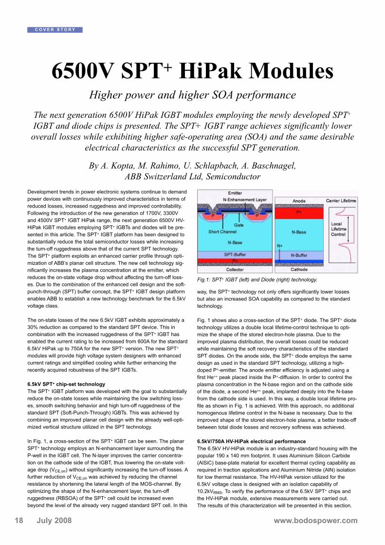
In Fig. 1, a cross-section of the SPT+ IGBT can be seen. The planar
SPT+ technology employs an N-enhancement layer surrounding the
P-well in the IGBT cell. The N-layer improves the carrier concentra-
tion on the cathode side of the IGBT, thus lowering the on-state volt-
age drop (VCE,on) without significantly increasing the turn-off losses. A
further reduction of VCE,on was achieved by reducing the channel
resistance by shortening the lateral length of the MOS-channel. By
optimizing the shape of the N-enhancement layer, the turn-off
ruggedness (RBSOA) of the SPT+ cell could be increased even
beyond the level of the already very rugged standard SPT cell. In this
way, the SPT+ technology not only offers significantly lower losses
but also an increased SOA capability as compared to the standard
technology.
Fig. 1 shows also a cross-section of the SPT+ diode. The SPT+ diode
technology utilizes a double local lifetime-control technique to opti-
mize the shape of the stored electron-hole plasma. Due to the
improved plasma distribution, the overall losses could be reduced
while maintaining the soft recovery characteristics of the standard
SPT diodes. On the anode side, the SPT+ diode employs the same
design as used in the standard SPT technology, utilizing a high-
doped P+-emitter. The anode emitter efficiency is adjusted using a
first He++ peak placed inside the P+-diffusion. In order to control the
plasma concentration in the N-base region and on the cathode side
of the diode, a second He++ peak, implanted deeply into the N-base
from the cathode side is used. In this way, a double local lifetime pro-
file as shown in Fig. 1 is achieved. With this approach, no additional
homogenous lifetime control in the N-base is necessary. Due to the
improved shape of the stored electron-hole plasma, a better trade-off
between total diode losses and recovery softness was achieved.
6.5kV/750A HV-HiPak electrical performance
The 6.5kV HV-HiPak module is an industry-standard housing with the
popular 190 x 140 mm footprint. It uses Aluminium Silicon Carbide
(AlSiC) base-plate material for excellent thermal cycling capability as
required in traction applications and Aluminium Nitride (AlN) isolation
for low thermal resistance. The HV-HiPak version utilized for the
6.5kV voltage class is designed with an isolation capability of
10.2kVRMS. To verify the performance of the 6.5kV SPT+ chips and
the HV-HiPak module, extensive measurements were carried out.
The results of this characterization will be presented in this section.
C O V E R S T O R Y
6500V SPT+ HiPak ModulesHigher power and higher SOA performance
The next generation 6500V HiPak IGBT modules employing the newly developed SPT+
IGBT and diode chips is presented. The SPT+ IGBT range achieves significantly loweroverall losses while exhibiting higher safe-operating area (SOA) and the same desirable
electrical characteristics as the successful SPT generation.
By A. Kopta, M. Rahimo, U. Schlapbach, A. Baschnagel, ABB Switzerland Ltd, Semiconductor
Fig.1: SPT+ IGBT (left) and Diode (right) technology.

19www.bodospower.com July 2008
The nominal rated current of the 6.5kV HV-HiPak module is 750A,
which corresponds to a current density of 34.3A/cm2 for the IGBT
and 77.5A/cm2 for the diode. For dynamic measurements, the nomi-
nal DC-link voltage was 3600V, while SOA and softness measure-
ments were carried out at 4500V.
In Fig. 2-a, the on-state curves of the 6.5kV SPT+ IGBT can be seen.
The typical on-state voltage drop (VCE,on) at nominal current and
Tj=125 °C is 4.0V. The SPT+ IGBT shows a positive temperature
coefficient of VCE,on, starting already at low currents, which enables a
good current sharing capability between the individual chips in the
module. In Fig. 2-b, the on-state characteristics of the 6.5kV SPT+
diode are shown. Due to the advanced plasma shaping utilizing a
double He++ irradiation scheme, the diode has a strong positive tem-
perature coefficient of VF already well below the nominal current. At
rated current and 125 °C, the diode has a typical on-state voltage
drop of 3.5V.
Fig. 3-a shows the turn-off waveforms of the 6.5kV HiPak module
measured under nominal conditions i.e. at 750A and 3600V. Under
these conditions, the fully integrated turn-off losses of the module
amount to 5.2J. The module was switched-off using an external gate
resistor (Rg,off) of 15Ω, which results in a voltage rise of 2000V/μs.
The optimized N-base region combined with the Soft-Punch-Through
(SPT) buffer allows the collector current to decay smoothly, ensuring
Fig. 2-a: Forward characteristics of the 6.5kV SPT+ IGBT (modulelevel measurements).
Fig. 2-b: Forward characteristics of the 6.5kV SPT+ Diode (modulelevel measurements).
Bicron Electronics Companywww.bicronusa.us1 800 624 2766, 1 860 824 5125In Europe—TransElectro, DK +45 9858 1022
HF Transformer Types:
When power control failure is not an option . . . . .

a soft turn-off behavior without any disturbing voltage peaks or oscil-
lations even at high DC-link voltages and stray inductances.
Fig. 3-b shows the turn-on waveforms under nominal conditions. The
low input capacitance of the planar SPT+ cell allows a fast drop of the
IGBT voltage during the turn-on transient. This, combined with the
low-loss SPT+ diode, brings the turn-on switching losses down to a
typical value of 6.4J. By carefully designing the diode cathode-sided
He++ peak, a short, but still smoothly decaying current tail was
achieved. Under nominal conditions, the diode recovery losses are
2.8J. Thanks to the high ruggedness and soft recovery behavior, the
diode can be switched with a high diF/dt, which significantly reduces
the IGBT turn-on losses.
In Fig. 4 the trade-off curve between the IGBT on-state voltage drop
and the turn-off losses for the SPT+ as well as the standard SPT
IGBT measured at chip level can be seen. The different points on the
technology curves correspond to IGBTs with different anode emitter
efficiencies. The devices were measured at a collector current of
25A, which is the nominal current of the SPT IGBTs. The new SPT+
IGBT exhibits an approximately 30% lower on-state voltage drop
(VCE,on) for the same turn-off losses as compared to the standard
SPT chip. The final point on the technology curve for the SPT+ IGBTs
was carefully selected based on the trade-off between reverse leak-
age current and turn-off softness while maintaining a good balance
between switching and conduction losses.
In order to evaluate the performance of the 6.5kV SPT+ module
under real application conditions a thermal simulation of the output
current as function of the switching frequency was made. The results
can be seen in Fig. 5. The 6.5kV SPT+ IGBTs have been optimized to
operate in an application environment with high stray inductances uti-
lizing low switching frequencies.
One of the main advantages of the new 6.5kV SPT+ IGBT is its
extremely high turn-off ruggedness, setting a new benchmark for this
voltage class. Fig. 6-a shows a turn-off waveform at module level,
where a current of 2400A, which corresponds to more than three
times the nominal current, was switched-off against a DC-link voltage
of 4500V at a junction temperature of 125°C. The test was conducted
with an external gate resistance of 1.0Ω, without using any clamps or
snubbers. The stray inductance in this test was 750nH, which is more
than double of that expected in the targeted application environment
even under worst case conditions. Thanks to the ruggedness of the
SPT+ cell, the IGBTs are capable of sustaining a long period of strong
dynamic avalanche during the turn-off transient showing an excellent
SOA capability. In this test the turn-off peak power reached a value of
11.7MW. In the standard production-level testing all modules are sub-
jected to a turn-off SOA test with three times nominal current (2250A)
C O V E R S T O R Y
20 www.bodospower.comJuly 2008
Fig. 4: 6.5kV SPT+ IGBT technology curve measured at chip level.
Fig. 5: 6.5kV SPT+ HiPak module output current as function of theswitching frequency.
Fig. 3-a: 6.5kV SPT+ IGBT turn-off under nominal conditions meas-ured at module level. Eoff=5.2J.
Fig. 3-b: 6.5kV SPT+ IGBT turn-on under nominal conditions meas-
ured at module level. Eon=6.4J.

where the modules are driven into dynamic avalanche. This very
harsh test has been implemented in order to ensure high quality and
reliability of all shipped 6.5kV HV-HiPak modules.
Fig. 6-b shows a diode reverse recovery SOA test at module level
measured with a forward current of 750A (nominal current) and a DC-
link voltage of 4500V. Due to the IGBT turn-on characteristics the
diode peak power reaches its maximum value close to the nominal
current and starts decreasing again for higher forward currents. The
diode was switched using an external gate resistor (Rg,on) of 1.2Ωreaching a switching speed of 7000A/us and a peak power of 9.0MW.
The short circuit waveforms of the 6.5kV SPT+ module can be seen
in Fig. 7. The IGBT was carefully designed to withstand a short circuit
at VGE=15.0V for all DC-link voltages up to 4500V and junction tem-
peratures between –40 °C and 125 °C. The desired short-circuit
ruggedness was achieved by optimizations of the SPT-buffer and the
anode emitter efficiency.
Finally, to verify the surge current capability of the 6.5kV SPT+ diode,
the HiPak module was subjected to 100 surge pulse with a magni-
tude of 9.9kA and pulse duration of 10ms (I2t = 523kA2s) as shown in
Fig. 8. After the 100th pulse, the module was electrically retested to
ensure that no degradation had taken place. In the subsequent
destruction test the single pulse surge current capability was deter-
mined. The diodes reached a peak current of 12.3kA, corresponding
to an I2t value of 705kA2s before failing. This excellent surge current
capability was achieved thanks to a combination of the strongly
doped P+-emitter and a low on-state voltage drop facilitated by the
optimum plasma distribution shaped by the double He++ irradiation
scheme.
www.abb.com/semiconductors
C O V E R S T O R Y
21www.bodospower.com July 2008
Fig. 6-a: 6.5kV SPT+ IGBT turn-off under SOA conditions measuredat module level. Ppoff =11.7MW
Fig. 8: 6.5kV SPT+ diode surge current waveforms at module level.
Fig. 6-b: 6.5kV SPT+ diode reverse recovery under SOA conditionsmeasured at module level.
Fig. 7: 6.5kV SPT+ IGBT short-circuit characteristics measured atmodule level.

July 2008
Compared to previous generation IGBTs operated at 20 kHz, trench
IGBTs have lower conduction and lower switching losses at the same
operating conditions. These devices are also rated for 175°C maxi-
mum junction temperature to increase design margin further. Positive
Vce(on) temperature coefficient allows easier paralleling of the
devices for higher inverter power applications. In addition, 100 per-
cent of the parts are clamped inductive tested (ILM) at 4x the rated
current to guarantee robustness.
Trench IGBT
One of the major improvements in IGBT designs is the introduction of
trench gate IGBT. In a trench IGBT, the gate is trenched down into
the p+ body region. This results in reduction of saturation voltage,
Vce(on), when the IGBT is conducting. Another major improvement in
trench IGBT is the deploying of a depletion stop layer which allows
thinner IGBT with reduced tail current at turn off.
Figure 1 shows parametric comparisons between planar punch
through (planar) IGBT and trench depletion stop (trench) IGBT of the
same dimensions. This table shows important parameters of the
IGBTs in 20 kHz application. Trench IGBT parameters are superior to
those of planar IGBTs. Comparing parameter differences on Figure 1,
trench IGBT’s advantages can be summarized as follows: lower con-
duction voltage, Vce(on), lower switching losses and lower steady
state thermal resistance (Rth) compared to planar IGBTs.
Power Dissipation at 20 kHz
Power dissipation difference at 20 kHz is analyzed in Figure 2. 20
kHz is typically used for DC-AC inverter in applications such as solar
or UPS inverters. Calculation shows that there will be up to 30 per-
cent reduction in power dissipation at 20 kHz. This reduction means
end-products can be designed smaller or more output power can be
obtained from existing power board assembly.
Short Circuit Requirements
In a typical DC-AC inverter, output inductors and capacitors filter out
20 kHz switching harmonics. This results in an output voltage that is
very close to a true sine wave. When the output of the inverter is
shorted, the output inductors will limit the rate of change (di/dt) of the
current into the IGBT. Current will ramp linearly and the protection cir-
cuit should detect an over-current condition which terminates signals
to the gates of the IGBTs. This condition is different from the one in a
motor drive application where a short circuit usually means direct
short of IGBT terminals without inductor to limit di/dt of the current.
The waveform differences are shown in Figure 3. The first oscillo-
scope waveform shows current ramps linearly when an output induc-
tor is present on the output of the inverter. The controller sets over
current limit at 12 Amperes and stops the gate signal to the IGBT
when this limit is exceeded. When current ramps linearly, the IGBT is
not saturated and voltage drop, Vce(on), across it is small (1.7V).
Therefore, the instantaneous power dissipation is also relatively small
at 20.4 Watts (12A x 1.7V).
Assuming that the controller takes 500 nano seconds to react to this
over-current condition, the increase in the junction temperature of the
IGBT is calculated to be 0.204°C above the steady state junction
temperature. This is assuming an instantaneous thermal resistance
of 0.01 °C/W and following the formula: dT = Zth x Pdissipation, where
dT is the increase in junction temperature, Zth is the instantaneous
I G B T
22 www.bodospower.com
600V Trench IGBTs Optimized for 20 kHz Operation
The new generation of 600 Volt IGBTs is targeted for DC-to-AC inverter applications.These new devices use Depletion Stop Trench technology to reduce both conduction and
switching losses in high frequency switching applications such as UPS and solar invertersenabling higher efficiency power conversion. These devices have been optimized for
switching at 20 kHz with low short circuit requirements.
By Carl Blake and Wibawa Chou, International Rectifier
Figure 1:. Comparisons of planar punch through with trench depletionstop IGBTs
Figure 2: Trench IGBT offers 30% power dissipation reduction com-pared to planar IGBT in a 20 kHz DC to AC inverter application.

23www.bodospower.com
I G B T
thermal resistance and Pdissipation is power dissipation on the IGBT
die. This increase in the junction temperature is insignificant in most
applications and the IGBT should be able to survive this condition
without any problem.
On the second waveform, there is no output inductor that limits di/dt
of the current. IGBT reaches its current saturation level almost at the
instant the short circuit occurs. The entire bus voltage is dropped
across the IGBT and power dissipation is very large. In this example,
the current saturates at 33 Amperes and the entire bus voltage of
400V is dropped across the IGBT. The instantaneous power dissipa-
tion is approximately 13.2 kilowatts (33A x 400V). Using the previous
formula, the increase in junction temperature will be 132 °C above
the steady state junction temperature. This increase is very signifi-
cant such that the gate signal to the IGBT must be extinguished
immediately to prevent catastrophic device failure.
600V trench IGBTs for 20 kHz inverter application offer a trade-off
between short circuit time and Vce(on). Typically, the higher the short
circuit time, the higher Vce(on) will be. However, since output inductors
are always present on the application, current ramps linearly when
the output is shorted. Therefore, short circuit time handling capability
of the IGBTs does not have to be as long as that for motor drive
applications. These trench IGBTs have 5 usec short circuit time at
room temperature and 3 usec at 150°C. This specification is sufficient
for modern protection circuit and controllers to detect abnormality on
the inverter and to terminate gate signals to the IGBTs to prevent cat-
astrophic failure. Increasing short circuit time is not necessary as it
will increase the Vce(on) significantly which reduces efficiency of the
inverter.
Paralleling and 175°C Operations
Since 600V trench IGBTs are based on depletion stop thin wafer
design, the temperature coefficient of the Vce(on) is positive, similar to
that of a power MOSFET. This means increasing junction tempera-
ture will increase Vce(on) of the IGBT. This has an advantage when
multiple IGBTs are put in parallel to increase power handling capabili-
ty of the inverter. With positive temperature coefficient, when one
device takes more current than the others, it will heat up more and its
Vce(on) will increase. When Vce(on) increases, current through the
IGBT will automatically reduce and current balance is automatically
restored. On punch through planar IGBTs without thin wafer design,
the temperature coefficient is negative. Increasing temperature of the
IGBT will result in reduction in Vce(on). It is, therefore, more difficult to
achieve current balance in parallel operation since the device that
takes more current will have its Vce(on) reduced and continues taking
more and more current leading to device destruction.
Another improvement made
on the 600V trench IGBT is its
capability to operate up to
175°C junction temperature.
This improvement allows
design engineers to have
more design margin for relia-
bility. It also means that the
device can provide more
power density out of the same
package. This allows design
engineers to provide more
output current capability out of
the same power board assem-
bly. On planar IGBTs, the
maximum junction tempera-
ture is limited to 150°C.
4x Clamped Inductive Load
On an inverter with inductor at the output, the IGBT will see high cur-
rent and high voltage simultaneously at the instant the device switch-
es off. This is due to the transition time of the IGBT from conducting
to blocking (usually specified as tdoff and tf on the datasheet) and par-
asitic inductances of the circuit. These inductances are shown in Fig-
ure 4 for clarity.
During transition time, current on the output inductor can not change
instantaneously. This means that current will continue flowing on the
co-pack diode of the complementary IGBT. However, it takes time for
the co-pack diode to conduct, during which time, the voltage across
the IGBT will spike above the bus voltage. This high voltage spike
will coincide with the high current to be turned off causing a lot of
power dissipation across the IGBT. In order to guarantee robustness,
600V trench IGBTs are designed to be able to turn off four times its
rated current. This is guaranteed by 100 percent testing each device
in production for clamped inductive load test. Typical waveform
across the IGBT at turn off transition is shown in Figure 5.
Conclusions
600V trench IGBTs offer several benefits compared to planar punch
through IGBTs. These advantages are increased power density,
increased reliability and ease of paralleling. This generation of IGBTs
is targeted for DC-AC inverter application at 20 kHz with low short
circuit rating requirements.
www.irf.com
Figure 3: Output inductor limits the rate of change of current into theIGBT when the output is shorted.
Figure 4: Output inductor and par-asitic inductors on a typical halfbridge inverter.
Figure 5:. Typical voltage and current across the IGBT at turn offtransition.

24 www.bodospower.comJuly 2008
In higher voltage applications, such as auto-
motive anti-lock braking systems, their com-
mutation speed allows them to be switched
on and off at very high frequencies, which is
a valuable asset in applications that use
pulse width modulation (PWM). However, the
growing spectrum of applications for high-
voltage MOSFETs – including high-efficiency
SMPSs (switched-mode power supplies),
industrial power converters and renewable
energy systems – creates a need for more-
efficient MOSFET technology. Superjunction
MOSFETs with higher breakdown voltages,
such as the Infineon CoolMOS™ 900V, meet
this need.
CoolMOS 900V power MOSFETs overcome
the “silicon limit” in power transistor manu-
facturing, and provide an alternative for high-
voltage designs using standard TO (Transis-
tor Outline) packages. The devices represent
the first time superjunction technology has
been extended to 900 V. They offer signifi-
cant performance capabilities that did not
previously exist, giving designers new ways
to think about implementing their high-volt-
age solutions.
Superjunction Technology
Conventional power MOSFETs today have
suffered from a “silicon limit,” which means
that doubling the voltage blocking capability
typically leads to an increase in the RDS(on)
(on-state resistance) by a factor of five.
With superjunction technology, the basic
idea is to allow the current to flow from top
to bottom of a MOSFET in very-high-doped
vertically arranged regions, so much more
charge is available for current conduction
compared to a standard MOSFET device
(Figure 1). In the blocking state of a super-
junction MOSFET, the charge is counterbal-
anced by exactly the same amount of
charge of the opposite type. The two
charges are separated locally in the device
by a very refined technology, and the result-
ing structure shows a laterally stacked fine-
pitched pattern of alternating arranged p-
and n-areas. The finer the pitch can be
made, the lower the RDS(on) of the device will
be. Infineon achieves the industry’s finest
pitch in its CoolMOS devices, yielding
benchmark-setting RDS(on) figures. Target
applications for the CoolMOS 900V MOS-
FETs are ATX (Advanced Technology
Extended) PC “silver box” power supplies,
quasi-resonant flyback designs for LCD TVs,
active 3-phase applications, solar converters
and other designs in which high blocking
voltage and low conduction and switching
losses combined with low gate charge are
necessary.
Device characteristics
Along with the world’s lowest RDS(on) per
package type for 900V MOSFETs (e.g., 120
mΩ in TO-247 and 340 mΩ in TO-220 pack-
ages), the Infineon CoolMOS 900V devices
have continuous drain currents of up to 36 A
and pulse currents of up to 96 A. They also
achieve a total gate charge (Qg) that is up to
25 percent lower than similar RDS(on) types.
This results in the lowest figure of merit, or
FOM (RDS(on) x Qg), in the voltage class,
which translates into low conduction losses,
easy driving and low switching losses.
In addition, the Infineon CoolMOS imple-
mentation of superjunction technology sets
new benchmarks for device capacitances.
The energy being stored in the output
capacitance is an effect that must be consid-
ered in the context of switching losses. This
energy, Eoss, is converted into heat during
hard-switched turn-on. Due to the strongly
nonlinear voltage dependence of the output
capacitance, the CoolMOS 900V devices
offer extremely good performance if switched
to more than 150 V. Energy stored in the
output capacitance of the MOSFETs is
reduced by a factor of two or more at the
working voltage.
The characteristics of the CoolMOS 900V
MOSFETs allow them to offer more design
flexibility, and let designers of power units
benefit from their high blocking voltage, low
RDS(on) and low Qg in a wide range of appli-
cations. Depending on the application, effi-
ciency can be increased and/or designs can
be simplified without additional costs or other
disadvantages.
M O S F E T
Renewable Energy Application Efficency
A new horizon for SMPS
Developed alongside such other power MOS devices as the IGBT, power MOSFETs havefilled niches for many applications. In lower voltage applications, they offer high efficien-cy for power supplies and DC-to-DC converters, and provide high stability in servo and
motor control designs.
By Dean Henderson, Segment Marketing Manager/Computing, Infineon Technologies North America
And Christian Wald,Senior Specialist, Regional Marketing Management, Infineon Technologies AG
Figure 1. Schematic cross-sections of stan-dard and superjunction power MOSFETs

25www.bodospower.com July 2008
M O S F E T
Single-Transistor-Forward (STF) Convert-
ers
The output power benchmark for STF con-
verters in PC “silver box” supplies can be
increased by using CoolMOS 900V MOS-
FETs. Up to 500 W is achievable with a sin-
gle MOSFET, with increased performance
and lower costs compared to standard two-
transistor-forward (TTF) converters using
200 mΩ 500 V/600 V MOSFETs (Figure 2).
The STF circuit uses only one transistor,
compared to the two transistors and pulse
transformer of a TTF, a topology change that
simplifies the design and adds layout bene-
fits without the disadvantages of TTF, such
as the need for high-side-switching.
Despite the higher RDS(on) of 900 V MOS-
FET, it is possible to design a STF with a
higher efficiency than a TTF that uses 200
mΩ 600V devices. This is due to the higher
dynamic losses in a TTF, in which in every
cycle two transistors have to be switched,
compared to only one transistor in an STF.
Also, the transformer in an STF converter
needs an additional demagnetizing winding,
which causes a small amount of losses that
do not exist in a TTF topology. Designs
using the 340 mΩ CoolMOS 900V have
been shown to reduce losses by up to 0.7
percent compared to TTF designs with 200
mÙ MOSFETs.
Quasi-Resonant Flyback
Converters for LCD TVs
Modern LCD TVs require out-
put power up to 200 W, with
high power supply efficiency
and low costs. The best
topology for these require-
ments is the quasi-resonant
flyback converter (Figure 3),
for which the CoolMOS 900V
is ideally suited.
Quasi-resonant flyback designs for LCD TV
power supplies can benefit from a higher fly-
back voltage, which provides a longer pri-
mary duty cycle with reduced peak current,
true zero-voltage switching and significantly
lower voltage stress on the secondary side.
Because of its very low RDS(on), a single
CoolMOS 900V MOSFET in a TO-220-FP
package can be used in such a design,
rather than the two or more TO-220-FP
packages that must be used with conven-
tional 900V MOSFETS. Efficiency improve-
ments of 0.2 percent compared to available
800 V parts, and of 0.7 percent compared to
standard 600 V/650 V parts, have been
demonstrated using CoolMOS 900V devices.
Renewable energy applications/solar con-
verters
In solar power generating systems, more
photovoltaic converter panels can be placed
in series instead of in parallel if the MOSFET
voltage is increased to 900 V, or solar panel
voltage window can be increased. This
series connection reduces cabling power
losses and costs, with cabling costs alone
cut by a factor of two when changing from
600 V to 900 V devices. In addition, Cool-
MOS 900V devices allow converters to be
designed with an enlarged input voltage
range, coming closer to the upper limit of
1000 V as defined by the IEC 60364 for
solar modules.
Another factor in photovoltaic systems is the
size and cost of magnetic components.
Offering a device with improved RDS(on) x Qg
and RDS(on) x Eoss performance allows an
increase of switching frequency without
increased losses. Therefore, a reduction of
system size is possible without losing energy
efficiency.
Lighting applications
Ballast designs for lamps that are fed from a
three-phase mains supply, such as special
discharge lamps used in comfort lighting and
electronic lamp ballasts for street lights and
greenhouse heating lamps, will also benefit
from topologies based on the CoolMOS 900
V family. The ballasts for such lamps require
a higher voltage capability than is offered
with 600 V or 800 V MOSFETs, as well as a
lower RDS(on) than is offered with convention-
al 900V MOSFETs. The CoolMOS 900V
devices allow improved design of PFC
(Power Factor Correction)
supplies and lighting ballasts
because they permit design-
ers to accept a higher DC
link or input voltage. For
example, high-power applica-
tions that use three-phase
PFC and PWM stages with
DC link voltages of up to 750
V will see such benefits as
higher power density from
having the industry’s lowest
RDS(on) in a small package,
such as the TO-247.
Conclusion
The key consideration with power MOSFETs
is how low can RDS(on) become at a particu-
lar breakdown voltage and in a given pack-
age. The introduction of superjunction MOS-
FETs at 900 V, with the lowest RDS(on) avail-
able at that voltage in a variety of small-
form-factor packages, gives designers of
high-voltage systems a new set of tools for
increasing switching speeds and perform-
ance while improving overall efficiency.
www.infineon.com
Figure 2a. Comparison of TTF and STF con-verter topologies (STF)
Figure 4. Typical DC/AC solar converter (with overvoltageprotection)
Figure 2b. Comparison of TTF and STF con-verter topologies (TTF)
Figure 3. Quasi-resonant flyback converter for LCD TV

26 www.bodospower.comJuly 2008
D I G I T A L P O W E R
Power engineers associated digital power
with fears of z-transforms, software coding
or blowing up power supplies due to “blue
screen of death”, as sometimes seen in a
particular computer operating system. Fur-
thermore, prior to the introduction of semi-
conductors that included all the functionality
necessary to digitally communicate and con-
trol a complex power system, the fundamen-
tal concepts were proven using high cost
DSPs or performance limited FPGAs. Even
though digital power techniques had demon-
strated the ability to raise power system per-
formance, the industry could not accept
mimicking digitally what was already being
done in analog at more than 10 times the
silicon cost. Much progress has been made
during the past several years and market
analysts as well as financial investors
appear very optimistic regarding the future
growth of digital power.
Today’s digital power market is made up of
numerous semiconductor suppliers and orig-
inal equipment manufacturers (OEMs) each
contributing unique solutions. It’s important
to first distinguish what is meant by digital
power. Power system supervision, monitor-
ing, fault detection and data logging is one
aspect of “digital power management” (DPM)
that can be implemented using an inexpen-
sive microcontroller, FPGA or PLD, where
the time base requirements are relatively
slow. However, the more challenging exam-
ple of digital power refers to “digital control
of power” (DCP) where one or more power
supply control loops are closed around a
high speed analog to digital converter (ADC)
and a micro-controller, state machine or
DSP-based control algorithm.
Semiconductor market research firm, iSuppli
estimates that the total world wide digital
power market will grow from its current 2008
revenue of just over $200M to about $900M
in 2011. The digital power rate of revenue
growth is summarized graphically in figure 1
indicating a progressive growth pattern with
DPM far outpacing DCP for the next several
years.
The majority of dedicated digital controllers
available to date are targeted for high vol-
ume, non-isolated, DC-DC power conver-
sion, including voltage regulator modules
(VRM) and point of load (POL) converters.
These types of DC-DC converters typically
deliver power to low voltage, high current
digital loads such as microprocessors, DSPs
and other high speed digital circuits that are
very dynamic in nature. It is becoming
increasingly difficult to maintain accurate
voltage regulation around 1V, while meeting
load transient requirements approaching
200A/ns using pure analog control tech-
niques. Some digital controllers can offer
certain features, such as non-linear control
which may be more difficult or impossible to
realize in an equivalent analog IC. In fact,
just about all digital POL controllers include
some distinguishing control technique aimed
at improving transient response. Since most
of these proprietary control algorithms were
developed by start-up venture companies,
the OEM’s demand for preferred suppliers
and dual sourcing became a barrier to gain-
ing market acceptance. This in turn has led
to licensing agreements between a number
of digital power start-ups and the more
established analog semiconductor suppliers.
Non-isolated, DC-DC POL applications are
viewed as a digital power entry point into the
power conversion market. However, it is
eventually expected that isolated DC-DC
and AC-DC power factor correction (PFC),
which currently implement digital control
using non-dedicated DSPs, will gain even
higher acceptance in coming years.
The functional requirements for a digital PFC
controller are much different compared to a
Digital Power on the MoveA Panoramic View of Applications and Challenges
When digital power first emerged as a topic of debate in the early 2000s, most power supply designers cast their doubts at the thought of replacing analog
PWM controllers with a DSP based digital power supply controller.
By Steve Mappus, Systems Engineer,Fairchild Semiconductor, High Power Solutions, Bedford, NH
Figure 1. Global Digital Power Semiconductor Revenue Forecast (Millions of U.S. Dollars)(Source: iSuppli Corp, December 2007)
$0
$100
$200
$300
$400
$500
$600
$700
$800
$900
$1,000
2006 2007 2008 2009 2010 2011
Rev
enue
in M
illio
ns o
fDol
lars
DPMDCP
Source: iSuppli Corp, December 2007

Mes
ago
Mes
sem
anag
emen
t G
mb
H, P
ost
fach
10
32 6
1, 7
0028
Stu
ttg
art,
Ger
man
y, s
ps@
mes
ago
.mes
sefr
ankf
urt
.co
m, p
ho
ne
+49
711
6194
6-82
8
Experience electric automationat its best!Come and see it all!Control TechnologyIPCsDrive Systems and ComponentsHuman-Machine-Interface DevicesIndustrial CommunicationIndustrial SoftwareInterface TechnologyElectromechanical Components and Peripheral EquipmentSensor Technology
Nuremberg
ElectricAutomationSystems and Components
Exhibition & Conference25 – 27 Nov. 2008
SPS/IPC/DRIVES/
www.mesago.com/sps

28 www.bodospower.comJuly 2008
POL controller. PFC regulators require less
load regulation accuracy and operate at a
lower switching frequency and lower overall
control loop bandwidth making quantization
errors, limit cycling and ADC resolution less
of a design challenge. Still, there are unique
design issues with PFC controllers demand-
ing significant system knowledge and experi-
ence. Although load transient requirements
and dead-time optimization are not concerns
for PFC, non-linear control could be useful
for handling line transient conditions which
are characteristic of virtually all off-line con-
verters.
AC-DC power supplies generally require an
electro-magnetic interference (EMI) filter
capable of attenuating noise generated by
harmonic distortion and switching regulators.
Since EMI filters are designed using net-
works of inductors and capacitors that
appear in series with the AC mains, they
have a negative effect on overall efficiency
but are necessary for meeting certain equip-
ment specifications. Some digital PFC regu-
lators can incorporate features aimed at
reducing EMI filter requirements, resulting in
smaller more efficient EMI filters. Analog
PFC controllers are distinguishable by vari-
ous control algorithms and operating modes
such as discontinuous conduction mode
(DCM), continuous conduction mode (CCM)
or boundary conduction mode (BCM). Each
PFC operating mode has advantages and
disadvantages that become more evident at
various power levels. Similar to the multi-
mode operation of a digital POL, a digital
PFC controller could be assigned to operate
in either PFC control mode. Whether for
PFC or POL applications, a controller that is
configurable across many OEM product plat-
forms provides value through faster develop-
ment time and less component inventory to
maintain.
Higher power AC-DC applications are better
candidates for digital power because they
require one or more PFC regulators as well
as multiple, isolated and non-isolated power
rails and complex cooling profiles. Server
power systems are one example where digi-
tal control and power management can offer
performance and efficiency benefits in a dis-
tributed power architecture (DPA). As more
digital power content makes its way into the
server and computing power segments,
other high power DPA systems such as
those used in telecom and datacom are
beginning to embrace digital power solu-
tions. The depth of present and forecasted
market penetration for all digital power semi-
conductors is clearly being led by these
types of high power applications, as shown
graphically in figure 2. Interestingly, recent
government and regulatory requirements for
PFC above certain power levels combined
with the falling costs of silicon for digital con-
trollers may enable the feasibility for digital
power development in some consumer ac-dc
power supplies such as game systems, set-
top boxes, digital televisions, AC adaptors
and battery chargers.
Regardless of analog or digital, power sup-
plies developed for consumer market appli-
cations are especially cost sensitive. The
cost pressure compared to existing analog
solutions has made digital power a tough
sell for consumer applications but some
industry analysts predict that within 2008 the
silicon cost of existing digital controllers may
approach price parity compared to similar
analog solutions. The value proposition of
digital power will never be compelling
enough if compared to a simple analog
power supply solution. One power supply
OEM in particular has designed a platform of
digital power solutions that has been shown
to beat their existing analog solutions in
terms of performance and overall cost.
Issues such as system complexity and pro-
prietary intellectual property demanded that
the proof come from within their own compa-
ny. The cost comparison between digital and
analog power solutions has to be looked at
from the entire system point of view includ-
ing: the cost of design, process develop-
ment, test, qualification, manufacturing,
inventory control and component savings.
Although wide market adoption of digital
power is still early in its infancy, there are
several key factors for acceptance that can
not be ignored. Tougher global efficiency
requirements beg the question: what can
digital power contribute towards increasing
efficiency? When implemented correctly, dig-
ital control can potentially offer some effi-
ciency improvements through duty cycle
optimization, adaptive shoot-thru control,
meeting transient requirements while
enabling lower switching frequency, real time
adaptation of critical timing such as synchro-
nous rectification or resonant dead time,
phase shedding and varying operating
modes based upon load current. Digital con-
trol can yield better overall efficiency results
because the system power is managed more
efficiently according to the demands of the
load. Any efficiency improvement is always
welcome but in order to set realistic expecta-
tions, it is important to emphasize that effi-
ciency is primarily determined by the power
stage design.
A reliable, easy to use graphical user inter-
face (GUI) is an essential requirement for
the success of any digital power controller.
Many power designers are quick to nod in
agreement at the thought of wanting all the
flexibility a digital controller can offer.
Enabling flexibility through hundreds of pro-
grammable commands requires careful con-
sideration in terms of software layers, parti-
tioning, protection features and command
grouping. The GUI needs to have an intu-
itive, natural feel but most importantly it
needs to work one hundred percent of the
time. Power supply design is difficult enough
without adding doubt as to whether the con-
troller is behaving the way it was pro-
grammed.
D I G I T A L P O W E R
Figure 2. Digital Power Semiconductor Market Penetration Rates (Source: iSuppli Corp,December 2007)
0%
5%
10%
15%
20%
25%
2006 2007 2008 2009 2010 2011
Pene
trat
ion
Perc
enta
ge R
ate Server dc-dc
Graphic CardTelecom dc-dcDatacom dc-dcComputing dc-dcac-dcLightingDigital TVTotal
Source: iSuppli Corp, December 2007

29www.bodospower.com July 2008
Digital controllers also need to be self-con-
figurable, meaning that no calibration should
be required by the end user. Some power
supplies are manufactured in an environ-
ment where the controller module and power
stage might be arriving from different suppli-
ers and are not integrated until final assem-
bly. In this case, there is no opportunity to
calibrate the controller since the power stage
is unavailable at the time of deliv-
ery.
Every digitally controlled power
converter inevitably requires a cer-
tain amount of analog circuitry.
Whether external or integrated into
the same package, gate drivers
are just one example of an inter-
face between the analog and digi-
tal domains. ADCs, voltage refer-
ences, regulators and comparators
are also required analog functions
that must perform seamlessly in or
around a digital controller.
Because there are numerous ways
to partition digital and analog func-
tions, obtaining the optimal bal-
ance between silicon performance,
efficiency, intelligence, cost,
process capability and die area
continually poses a difficult chal-
lenge for system engineers. In ret-
rospect, the concept of digital
power is really nothing new or rev-
olutionary. DSPs and microcon-
trollers have been widely used in
industrial motor control applica-
tions for many years. The power
supply industry has been inching
toward digital power adoption but
the necessary standards and dedi-
cated semiconductors were not
available until recently.
Digital content such as combina-
tional logic, clocks, counters and
timers have always existed inside
analog controllers. As mixed signal
design processes continue to
improve, expect the relationship
between digital and analog compo-
nents to be optimized to a much
higher degree. Depending on the
complexity of a targeted applica-
tion, some functions would benefit
best from a digital process while
others should remain in the analog
domain. At least in the near term,
the most cost-effective, optimal
solutions appear to be mixed sig-
nal approaches no matter how “digital” a dig-
ital power system becomes. The fundamen-
tal groundwork necessary for shaping the
landscape of digital power is in place but
there are still questions remaining as to how
digital power will complement or compete
with traditional analog solutions. Most
accomplished power supply designers who
recognize the value of digital power will
update their design skills accordingly but
regardless of different viewpoints on adop-
tion rates, one thing is certain: digital power
is inevitable.
www.fairchildsemi.com
D I G I T A L P O W E R
deadline for submission, July 18, 2008, go to web for details:
www.apec-conf.orgwww.apec-conf.org
CALL FOR PAPERS!CALL FOR PAPERS!
SPONSORED BY
2009February 13–21, 2009
Washington, DC
THE PREMIER
GLOBAL EVENT
IN POWER
ELECTRONICSTM
THE PREMIER
GLOBAL EVENT
IN POWER
ELECTRONICSTM

30 www.bodospower.comJuly 2008
Where it makes sense.
Before the term „Digital Power“ was ever coined, it has been used
since decades whenever it made sense, i.e. in large power supplies,
especially in those destined for complex installations. However, the
term DP as it is used and advocated now applies to the replacement
of analog control by digital control using DSP’s resp. mixed chips in
all SMPS. This means to exchange something perfectly and reliably
functioning at low cost by something much more expensive, less reli-
able and without any tangible advantage. This is exemplified by the
quality and tenor of the „pushers‘“ arguments.
Quality of arguments for Digital Power (DP).
The abuse of the term „digital“ as a synonym for superiority like „digi-
tal is better than analog“ is marketing hype; scrutiny of the claims of
the DP pushers yields a list of major disadvantages for the vast
majority of SMPS. The pushers overlooked that all SMPS in the past
60 years functioned perfectly without DP which says enough about
the need for it
„Naturally, the digital loop concept is driven by the start-ups in the
power industry.“ In other words by people with zero or rudimentary
knowhow and experience in power design.
After conceding: „System makers push the market“, an analyst states
bluntly: „Analog technology cannot avoid becoming obsolete“, „Many
in the analog community do not appreciate the impact of Moore’s
Law and do not understand that the fate of analog power technology
is already determined.“ He concludes that DP ic’s will fast become
less costly than analogue ones and this would force total conversion.
Obviously, he assumes that SMPS consist of circuit boards full of ic’s.
Another analyst : „The analog designers’ identities seem to be tied up
with their black-art experience in analog; it’s just too scary or painful
to imagine that such knowledge might not be valuable in the near
future. However, the analog suppliers find themselves very much in
the same position as mom-and-pop grocery stores in the US...“
A DP pusher: „Before the advent of DP, hardware engineers were for-
ever tweaking and experimenting with different design approaches to
solve anomalies...“
Arguments of such quality are none but insults, and it remains the
secret of these authors why they consider insults the most effective
method of convincing prospective customers. Calling analog design a
„black art“ denounces professional engineering, not understanding
that analog design is immensely more difficult than digital design, the
latter being nothing else but a primitive reduced form of analog
design!
Claim 1: DP reduces costs, also SMPS can now be designed
within minutes.
Starting from the indisputable fact that present SMPS function per-
fectly well, the only salient argument for introducing DP would be
lower cost. Costs rule, and as long as a DP ic replacing a TL 431
costs more than this, i.e. a few cents, this claim remains false, even if
DP ICs would be given away, this would not materially affect the
BOM of a SMPS; it is the inductive and capacitive components, the
power semiconductors, the e.c. board, housing, connectors which
head the bill, the cost of the control chips is absolutely zilch. The
claim that with DP „a SMPS can now be designed within minutes“ is
utterly absurd: most of the design effort is and will remain devoted to
the design of the major components like transformers, the placement
of components, the conductor layout and testing; the design work to
fulfill the emi norms may take up a sizeable portion of the whole
design costs and time. The design of the control loops is not even
worthwhile mentioning.
Costs rule, this fact will prevent widespread use of DP, the cost
squeeze being extreme. It is astonishing why DP proponents still
wonder why the „breakthrough“ they predicted just doesn’t happen,
they just forgot about cost, underestimated the intelligence of SMPS
designers, also they never mentioned the disadvantages and dan-
gers!
Claim 2: DP is more reliable.
In all articles this author encountered, the serious dangers of using
today’s digital ic‘s inside a SMPS were omitted. In fact, there is no
environment more hostile to digital circuitry! There are extremely
strong magnetic and electric hf fields beyond 100 MHz emanating
especially from inductive components but also from others and the
conductors. And it is just the continuing shrinking of digital ic’s with
ever lower voltages down to below 1 V and higher speed which
makes them increasingly vulnerable to interference and hence unfit
for use inside a SMPS. Most SMPS are extremely densely packed.
„Obsolete“ fairly „slow“ 12 V CMOS ic’s with their 6 V threshold are
quite safe even close to 800 V signals with rise times of under 10 ns
and are being used since decades; there is nothing new about digital
circuitry in SMPS whereever it was appropriate, e.g. for generating
multiphase signals.
This problem is aggravated by the fact that microcomputers/ DSP’s
are basically highly vulnerable to interference: while analog or other
digital logic will either ignore an interference pulse or react at most
with a short hiccup, a single pulse disturbing any of e.g. 32 address
lines will cause the program to fetch from a wrong memory location,
so e.g. an add instruction will be replaced by e.g. a branch instruction
with catastrophic consequences. If an interference disturbs a data
bus or control signal, equally fatal results will ensue. But even without
the influence of interference, plain software errors will lead to disas-
trous failures, especially in high power supplies. Due to the nature of
these problems it will be close to impossible to ever reconstruct the
cause of the failure! A bit further down into the nitty-gritty: the inputs
and outputs of CMOS ICs must be protected against exceeding Vcc
or ground levels by more than 0.3 V; if this is not strictly observed,
arbitrary malfunctions or total failures may result. Interference pulses
are not only present during „normal“ operation, but especially during
start-up, overload or short-circuit conditions not to speak of extremely
high interference from the mains and the environment. Many SMPS
are not shielded, due to the high frequencies of cell phones any con-
ductor of a few centimeters may pick up high levels of hf which would
not affect properly designed analog circuits but well microcomputers
or DSP’s running at speeds of several hundred MHz, generating by
the way also additional highly undesirable emi.
G U E S T E D I T O R I A L
Digital PowerHope or Hype?
By Dr.– Ing. Artur Seibt, Vienna

Inside a SMPS temperatures run anywhere from 60 to over 100
degrees; transformers are designed for 100 degree operation. Such
ambient temperatures are detrimental to microcomputers/ DSP’s; the
usual answer that such chips are also used in cars disregards the
fact that the actual operating life of a car is just a few thousand hours
while a standard SMPS is expected to operate for 5 to 30 years! (Not
all electronics are pc’s designed for 2 years.) Here, another basic
severe problem of all present digital ic’s comes in: after a few years
they will no longer be available, hence a repair of a defective SMPS
will become impossible.
In case of malfunction of a DP ic, the state of its ports may become
any; if e.g. the drive signal of a power FET lasts a few microseconds
too long, it can destroy the FET. How do the proponents of DP guar-
antee that any conceivable malfunction will be automatically detected
and corrected within at most a few microseconds? The benefits of
DP in a cell phone may be real, but 3.6 V DC and 230 V AC with the
full power of the mains behind are two different stories. No type of
fuse or electronic circuit can prevent some components of a SMPS
from burning, e.g. capacitors and inductors. Analog circuitry is by
nature extremely reliable, anybody planning to replace it by some-
thing inferior should first learn about product safety and manufactur-
er’s liability and think twice about it! In EU, the liability is squarely on
the manufacturers!
In Germany e.g., the highest court (Bundesgerichtshof) ruled in 2004
that a person who suffered damage by a product could not only sue
the company but additionally all managers of that company who
decided upon product safety! The author has seen many managers‘
faces fall after they were presented with this court verdict!
As long as the „pushers“ of DP could not prove that their products
resp. circuitry are of equal reliability, they better abate their marketing
hype or give in writing that they will defend their customers in all
cases of product safety litigation.
Claim 3: DP offers better performance and higher efficiency.
Speaking about „better performance“ resp. „higher efficiency“ the first
question is which SMPS was taken as the reference for this claim, an
old-fashioned and poorly designed one?
The performance and the efficiency of a SMPS are determined
entirely by the circuit concept and the proper design resp. selection
of the vital components which is indeed an art but not a black one but
a professional one. Efficiencies of off-line PFC’s run from 96 to 98 %,
of combined PFC plus main converter SMPS from 87 to to > 90 %,
without DP, of course. Any further increase will require better compo-
nents. Low efficiency has nothing to do with the control loop but with
poor design and cheap components; no DSP in the control loop can
compensate for a poor transformer. Also, a properly designed SMPS
will function over its full line and load ranges down to no load with
standard analog control circuitry, a „change of parameters“ claimed
as necessary by the DP pushers is superfluous, it may be advanta-
geous in KW SMPS which constitute only a small fraction of the
SMPS population.
Summary.
Unless DP pushers can prove that their products save costs or offer
better performance so badly needed that customers are willing to pay
for it, it will fail; no customer will pay a cent more for „digital control“.
http://members.EUnet.at/seibt
31www.bodospower.com July 2008
www.kolektormagma.com [email protected]
ferrite cores
inductive components
absorber sheets
nanomaterials
www.h2expo.com
International Conference and Trade Fair on Hydrogen and Fuel Cell Technologies
22–23 Oct. 200822–23 Oct. 2008CCH – Congress Center Hamburg · Germany
Register online!

32 www.bodospower.comJuly 2008
White light can come from a single white
LED or be generated by three separate R-G-
B LEDs with a color spectrum that closely
matches the color filters of the LCD pixels.
This results in a great improvement in light
efficiency and a wide color range for a more
vivid display. Currently LCD with CCFL back-
light can generate only 70-80% of NTSC col-
ors while newer displays based on LED
backlight will generate all the colors in the
NTSC specification plus additional colors. By
using the ultra-fast switching time of LEDs,
the backlight intensity can be modulated to
enhance picture contrast and reduce the
smearing effect due to fast-moving images.
To replace CCFL in small size (19” typical)
LCD monitors, tri-color LED devices can be
deployed alongside the housing to replace
the CCFL tubes. Typically, only the light
source (from CCFL to LED strings) is
changed; the housing, light guide and optical
films remain unchanged. For larger size LCD
(20” or above), where higher light throughput
is required, an LED matrix can be deployed
directly behind the LCD panel. The matrix
size, typically in hundreds, varies in accor-
dance with panel size. To ensure homoge-
neous illumination, a special diffractive dif-
fuser is used over standard optical film. As
LED technology improves, the number of
LEDs in the string or matrix can be reduced
as luminous output (lumens/W) increases,
further reducing overall material and system
cost.
Of course, there are challenges to deal with,
such as maintaining spectral consistency
due to temperature change and the rate of
LED aging. However, the future is promising.
Key players in the portable electronic indus-
try plan to roll out more models with LED
backlight. Large screen TV manufacturers
have committed resources to make LED
backlight more popular in the consumer mar-
kets.
There has been a recent breakthrough in
backlight panel technology – the utilization of
the newly available high-brightness white
LEDs in a backlighting panel for LCDs.
These new LEDs require a 4 Vdc power
supply at 200 W in a very small package
size. This design is based on the patented
technology of a company that develops and
markets innovative High Dynamic Range
(HDR) image technology. This technology
makes it possible to build much brighter dis-
plays, as much as ten times brighter than a
conventional LCD, by using intensive video
processing algorithms to adjust the bright-
ness of the LEDs. Every single LED in the
backlight is individually addressable so the
light levels can be changed dynamically
frame by frame and specifically microregion
by microregion. This technology for
P O W E R S U P P LY
Flexible, Accurate & EfficientPower Solutions for LED Backlighting Applications
V•I Chips enable high-current, low-voltage distribution inside displays
Traditionally, large size LCDs (liquid crystal displays) used CCFLs (cold cathode fluores-cent lamps) as the source of backlight to achieve a uniform white light. Using LEDs
(light-emitting diodes) as backlight is gaining share at key manufacturers as LED outper-forms CCFL in size, energy efficiency, spectral purity, mechanical ruggedness, reliability
and the elimination of hazardous substances such as mercury.
By Steve Oliver, VP, V•I Chip Inc. (a Vicor company)

enhanced dynamic range displays enables
them to display pictures much more vividly
with much darker darks and much brighter
brights than previously possible. An existing
application involves large-format displays (37
inch and 46 inch high-definition displays) for
high-end imaging applications.
New architecture
These new LEDs require a 4 Vdc @ 200 W
power supply in very small package size.
Earlier designs were powered from a 5.5 V
power supply at 500 A, an unwieldy amount
of current to distribute around inside the dis-
play due to I2R distribution losses with asso-
ciated large and expensive cabling and con-
nectors.
A V•I Chip™ BCM™ bus converter is now
designed into this high-power LED applica-
tion to address the current distribution issue.
The BCM utilizes a patented Sine Amplitude
Converter (SAC) topology with state-of-the-
art power density, efficiency and low noise.
With a footprint of just 1.1 in2 and weighing
15g, the BCM converter provides an isolat-
ed, stepped-down voltage to power niPOLs
(non-isolated point of load converters), in
this case LED driver ICs. Due to its fast
response and low output noise, the need for
limited life bulk capacitors at the load is
reduced or eliminated, resulting in saving of
board space, materials and total system
cost.
Now the system distributes 48 V everywhere
at a much lower current. At the point of load,
it is locally stepped down to high-current at
4 V. On each of the large format boards
there are four boards in one system. In total,
there are 16 BCM modules running in each
system. The result is 4 V at 200 A on each
board. In contrast, the previous design using
the large centralized power supply would
need to provide 800 A for each board incur-
ring significantly more distribution losses. Of
course, such a supply is dangerous as well
due to the high currents involved. That is
why 20 A of 48 V are distributed to each
board, which is much more manageable and
quite fusible.
Well-suited solution
Several factors make the BCM converter the
right solution. First, due to the small size and
high efficiency (>94%), no special heatsink-
ing is required. Second, it runs at 48 V – an
easily routed, safe (SELV) voltage. There is
a family of BCM devices providing different
standard output voltages which are optimal
for different applications. Typically, in the
LED backlight application, the downstream
LED driver ICs require an input voltage
trimmed to 4.1 to 4.2 V. As the BCM module
is an unregulated converter and not a regu-
lator, designers are able to increase the
input voltage to get to the designated output
voltage.
Other LED Backlight Options
Providing a Constant Current for PoweringLEDs
Other backlights may require a constant cur-
rent driving an array of high-power LEDs
connected in series. Generally, constant cur-
rent is required to ensure predictable lumi-
nosity and chromaticity levels. PRM™ regu-
lators and VTM™ voltage transformers,
though originally designed to provide a regu-
lated voltage from an unregulated input, are
able to provide an extremely efficient and
accurate constant current with a simple feed-
back circuit.
In a traditional DC-DC converter – the func-
tions of regulation and voltage transforma-
tion are combined limiting the ability to opti-
mize the system. The PRM regulator and
VTM transformer are individual components
and can be separated or ‘factorized’ to
enable higher power densities, higher effi-
ciencies and more efficient, flexible system
designs.
Using the PRM regulator and VTM trans-
former for constant current provides several
advantages over conventional approaches.
The implementation of a VTM module pro-
vides point-of-load current multiplication as
the output current is proportional to its input
current by the following equation:
Where K is the K-factor (transformer ratio) of
the VTM module.
Thus in a controlled current application, the
input current to the VTM transformer can be
sensed and regulated to control the output
current. Sensing a lower current (at a higher
voltage) requires a smaller sensor which dis-
sipates lower power and improves overall
efficiency. Also, as the V•I Chips themselves
provide high efficiency and high power den-
sity, this makes the overall LED system
small, cool and maximizes the output in
lumens per watt of dissipation – more than
>1,000 Lumens emitted per 1 Watt dissipat-
ed by the V•I Chips. The overall system
architecture is illustrated in Figure 2.
Most LEDs can be driven with a single PRM
+ VTM pair. The PRM regulator is pre-con-
figured with an internal voltage loop to regu-
late its output voltage to a set value. The
external constant current circuit is designed
to work in conjunction with the internal volt-
age control loop, changing the PRM voltage
reference in order to regulate the VTM out-
put current.
IOUT IIN
K
33www.bodospower.com July 2008
P O W E R S U P P LY
Figure1. Using a 48 Vin BCM to drive a white light LED
Figure 2. Regulated Current Source Basic Architecture
=

34 www.bodospower.comJuly 2008
A simplified block diagram of the PRM internal voltage control loop is
shown in Figure 3.
Here, an internal reference is generated and connected to the SC
(secondary control) port through a 10 k resistor and a 0.22 μF capac-
itor, which provides a soft-start. The SC voltage can be adjusted by
adding an external resistor or by applying an external voltage.
The SC voltage is buffered and fed to the error amplifier through a
resistive divider represented by the gain block of 0.961. R68 forms
the top half of the voltage-sensing resistive divider. The bottom half
of the divider is formed by adding a resistor from the OS pin to SG
(ROS). Equation 2 defines the regulator output as a function of VSC
and ROS. From Equation 2, it is seen that for a given ROS resistor,
adjusting the SC voltage will determine the output voltage. This is the
method by which the external current control circuit will control the
output.
Where:
VSC is the voltage at the SC pin.
ROS is the resistance from OS to SG
of the PRM regulator.
R68 is the internal resistor.
Current Control Circuit
The recommended current control circuit is shown in Figure 4. As the
VTM transformer is a current multiplier, the output current can be reg-
ulated by its input current. The advantage of this approach is that the
current can be sensed prior to the current multiplication stage (at the
higher voltage), reducing the I2R power dissipation in the external
shunt. In addition, the control circuitry remains on the primary side
(linked to the PRM regulator’s output), eliminating the need for isolat-
ing the feedback signal.
The circuit consists of a voltage reference, shunt resistor, differential
amplifier, and error amplifier. Low-side sensing is implemented at the
output of the PRM using an op amp configured as a differential
amplifier. The voltage across the shunt resistor (R1) is sensed and
amplified with a gain determined by resistors R2 through R5. The ref-
erence voltage is generated using a precision adjustable shunt refer-
ence, and is tied to the non-inverting terminal of the error amplifier.
This is the voltage to which the error amplifier will compare the differ-
ential amplifier output (VSENSE). The output of the error amplifier
(VEAO) is tied to SC through resistors R7 and R8, allowing for the
adjustment of the regulator’s output set point. The error amplifier will
adjust the PRM output voltage until VSENSE is equal to the reference
voltage VREF. This forces the VTM transformer’s input current, and
hence, its output current to be constant as determined by the VREF.
The resulting current may be 99.7% accurate directly from the PRM
regulator and up to 98.7% when measured at the VTM transformer
output, as shown in figure 5.
A single PRM regulator with a simple external current sense circuit
can be used as constant-current source (at 26 - 55 V). The VTM unit
transforms this ‘factorized’ bus voltage to the voltage that matches
different color LEDs from 0.8 to 55 V (for instance, 6 V for a blue
LED, 14 V for amber and 24 V for green – though this varies by LED
manufacturer).
The flexibility of Factorized Power Architecture (FPA) allows the
same regulator to drive different transformers (of different K factors)
for different color LEDs. Also, if the LED color voltage requirement is
constant, the same VTM transformer may be used while the PRM
regulator may be changed for a different input source voltage. Fur-
thermore, by ‘factorizing’ the conversion, only the VTM transformer is
required at the LED load, minimizing the voltage droop and power
dissipation. The PRM regulator may be placed elsewhere, perhaps
on a separate PCB and linked via a cable or a connector.
Conclusion
V•I Chips represent an accurate, highly efficient, low profile power
train for LED backlighting and illumination applications. Depending on
the LED configuration (individual or in higher power ‘strings’), the
OS
OS68SCOUT
R
)R (R x V x 0.961PRM_V
+=
Figure 3. Functional Diagram of PRM Internal Error Amplifier
Figure 5. Current Source Accuracy (PRM regulator alone providing
48 V)
Figure 4. Constant Current Circuit
P O W E R S U P P LY

BCM converter or the combination of PRM regulator and VTM trans-
former provides the optimal solution, as shown in Figure 6 as an
example.
PRM, VTM, BCM, Factorized Power Architecture (FPA), Sine Ampli-
tude Converter (SAC) and V•I Chip are trademarks of Vicor Corpora-
tion.
The Application Note: 018, Providing a Constant Current for Power-
ing LEDs using the PRM and VTM is available
at:www.vicorpower.com/ccdemo
www.vicorpower.com
Figure 6. LED Options Powered by V•I Chips from 48 V
E M C C O M P O N E N T S I N D U C T O R ST R A N S F O R M E R SR F C O M P O N E N T SP R E S S - F I T T E C H N O L O G Y C O N N E C T O R S V A R I S T O R SA S S E M B LY T E C H N I Q U E www.we-online.com
24h sample servicefor customized transformer
8-days-service free of charge
10 customized samples
Rapid prototyping
Designed to your specification
Including datasheet & test report
www.we-online.com/speedy
For Power & Telecom Transformers
Tape Wound CoresBobbin Cores
Cut Cores
Kool Mu® CoresMolypermalloy Cores
High Flux CoresXFLUX™ Cores
Power MaterialsHigh Permeability Materials
Special Materials
Strip Wound Cores
Powder CoresFerrite Cores
110 Delta DrivePittsburgh, Pa 15238
Toll-Free: 1 800 245 3984Phone: 412 696 1333Fax: 412 696 0333
Web: www.mag-inc.comEmail: [email protected] Magnetics Hong Kong
Asia Sales and Service
Phone: +852 3102 9337Fax: +852 3585 1482
Email: [email protected]
36 www.bodospower.comJuly 2008
For makers of advanced camera phones,
delivering the high peak current consumed
by high-intensity camera flash is of utmost
importance. As resolution of camera phones
grows to three megapixels and beyond, the
amount of light required to achieve a high
quality image has sharply increased. In order
to match the photo quality of digital still cam-
eras, cell phones must either drive flash
LEDs at currents as high as 2A or Xenon
flash tubes charged to over 330V. Other
applications in the phone such as the RF
power amplifier, GPS mapping, internet
access, music and video can also exceed
source current availability.
Design Challenges
Camera phones require a high intensity flash
in medium to low light conditions to produce
good pictures. Designers can choose either
LED or xenon flash units, but there are chal-
lenges with each:
High-current Flash LEDs need up to 400%
more power than a battery can provide to
achieve the light intensity needed for high-
resolution images. To overcome this power
limitation some camera phones have used
long flash exposure times to compensate for
the lack of light, resulting in blurry photos.
Xenon flash tubes deliver good light power,
but have a short flash exposure and can’t be
used for a video capture/movie-mode func-
tions. The required electrolytic storage
capacitors are very bulky for slim-line
designs, operate at high voltages, take a
long time to recharge between flashes and
cannot be used for other peak-power needs
in the phone.
One way to solve the problem with Flash
LEDs driven at 1 to 2A each is to use a
capacitor to store the current and deliver it
quickly without draining the main battery.
However, the use of conventional capacitors
would require either a very large case size
or multiple devices connected in parallel. A
more practical solution for space-constrained
portable systems is to use very high value
“super” capacitors. These devices offer high
levels of capacitance in a relatively small, flat
case size. By using a super capacitor,
designers can deliver the high current levels
needed for these short duration events and
then recharge from the battery between
events. To support the battery, designers can
add a thin super capacitor to handle the
phone’s peak-power needs – flash photos,
audio and video, wireless transmissions and
GPS readings – without compromising slim
handset design. It also allows the designer
to reduce the system footprint by optimally
sizing the battery and power circuitry to
cover just the average power consumption
instead of peak levels.
Defining a super capacitor
What is a super capacitor (SC)? Like any
capacitor, a super capacitor is basically two
parallel conducting plates separated by an
insulating material known as a dielectric. The
value of the capacitor is directly proportional
to the area of the plates and inversely pro-
portional to the thickness of the dielectric.
Manufacturers building “super” capacitors
achieve higher levels of capacitance while
minimizing size by using a porous carbon
material for the plates to maximize the sur-
face area and deploying a molecularly thin
electrolyte as the dielectric to minimize the
distance between the plates. Using this
approach they can manufacture capacitors
with values from 16mF up to 2.3F. The con-
struction of these devices results in a very
low internal resistance or ESR (Equivalent
Series Resistance) allowing them to deliver
high peak current pulses with minimal droop
in the output voltage. These super capacitors
reduce system footprint requirements by
delivering a very high capacitance in a rela-
tively small case size. They can be manufac-
tured in any size and shape and recharge in
seconds. By averaging high power
demands, they extend battery life by up to a
factor of five and allow designers to specify
much smaller, lighter and less expensive
batteries.
Inherent challenges
That low ESR presents designers with an
inherent problem during the charge cycle,
however. In any system the capacitor is ini-
tially discharged. When the supply voltage is
then applied, the super capacitor looks like a
low value resistor. This can result in a huge
in-rush current if the current is not controlled
or limited. Therefore, designers must imple-
ment some sort of in-rush current limit to
ensure the battery does not shut down. Any
circuit of this type also typically requires
short-circuit, overvoltage and current flow
protection.
The challenge for designers is how to effi-
ciently interconnect the battery, DC/DC con-
verter and super capacitor in a way that will
limit the super capacitor inrush charge cur-
rent and continually recharge the cap
between load events. LED flash drivers that
Super CapacitorReference Design
LED flash power issues for high resolution camera phones solved
Cell phones are becoming the ultimate converged consumer portable appliance. Capabilities include capturing high-quality photography, Wi-Fi web access, crisp audioand extended talk time along with longer battery life. A major design challenge is nowemerging. A phone battery still struggles to provide enough peak power to drive some
highly-complex mobile applications, driving the demand for circuits that can store highcurrents for short periods without overloading the battery to provide the power required
for high performance operation.
By Thomas Delurio, Applications Manager, Advanced Analogic Technologies, Inc
C A P A C I T O R S


38 www.bodospower.comJuly 2008
C A P A C I T O R S
can manage super capacitor charging requirements have appeared
on the market to make the designers’ jobs easier, integrating the cir-
cuitry to save space, cost and time to market. Flash LEDs for digital
still cameras require 1 to 2A for up to 120mS.
A super capacitor can be used to store the required current and deliv-
er it quickly without draining the main battery. Working together with
the battery, the super capacitor discharges its power during peak
loads and recharges between peaks, providing the power needed to
operate systems from battery operated hosts up to 200% longer
while extending the life of the battery. Clearly, any time designers use
a super capacitor, they must limit in-rush current. Moreover, the super
capacitor needs to be recharged when the voltage drop or droops
below the operational limit of the LEDs. When the SC is fully
charged, it has to be disconnected from the source. Short circuit pro-
tection, source over voltage protection and current flow protection are
also required.
Benefits
Conventional capacitor technology would require either a very large
case size or multiple devices connected in parallel to achieve high
capacitance values. Super capacitors recharge in seconds with
>500k Cycles and store energy in an electrostatic field as opposed to
a chemical state like a battery. Since voltage does not droop exces-
sively until heavy load currents when fully charged, the use of a
super capacitor also reduces ESR and impedance.
Super capacitors can be manufactured in any size and shape, flat
and small size. They can be used to extend battery life by five times
by ‘averaging out' high power demands so they allow smaller, lighter
and cheaper batteries. Super capacitors also have a long life (10 to
12 years). Unlike a battery, they have an open-circuit (high ESR) fail-
ure mode that is not destructive. Similarly, if over-voltage is applied to
the device, the only consequence will be a slight swelling and a rise
in ESR, eventually progressing to an open circuit. There will be no
fire, smoke or explosion.
Design Solution
Super capacitor-powered LED flash units can drive high-current
LEDs to provide light intensity that is many times greater than stan-
dard battery-powered LED flash units or longer than xenon strobes.
In the block diagram shown in Figure 1, the AAT1282 contains a
step-up converter used to boost the 3.2V-to-4.2V battery input volt-
age up to a constant 5.5V. If the battery voltage is 3.5V and the boost
converter is 90% efficient, the battery would need to supply over 3A
for the duration of a 2A flash pulse. This will either cause the battery
protection circuit to shut the battery down or cause a low voltage
shutdown while plenty of energy still remains in the battery. This solu-
tion also offers flash management capabilities, such as movie-mode,
and super-capacitor charging capabilities. The solution controls and
regulates the current from a cell phone’s battery source, steps up the
battery voltage, and manages the charging of a super cap, for the
control and supply of high-current to flash LEDs In the end applica-
tion.
To better achieve this, the step-up converter features built-in circuitry
to prevent excessive inrush current during start-up as well as a fixed
input current limiter of 800mA and true load disconnect after the
super capacitor is charged. The AAT1282 boost converter’s output
voltage is limited by internal overvoltage protection circuitry, which
prevents damage to the AAT1282 converter and the super capacitor
from an open LED (open circuit conditions). During an open circuit,
the output voltage rises and reaches 5.5V (typical), and the OVP cir-
cuit disables the switching, preventing the output voltage from rising
higher. Once the open circuit condition is removed, switching will
resume. The controller will return to normal operation and maintain
an average output voltage. An industry-standard I2C serial digital
input enables, disables LEDs and sets the movie-mode current with
up to 16 movie-mode settings for lower light output.
In figure 2, a detailed schematic illustrates that few components are
required, An 0.55F, 85mOhm super capacitor delivers 9W LED
power-bursts using the AAT1282 LED Flash driver which has the SC
charger integrated with the Boost DC/DC LED Driver. To achieve high
light levels, the flash LEDs are driven at currents of between 1A and
2A. The forward voltage (VF) across the LED at these high currents
can range up to 4.8V. If we include 200mV of overhead for the cur-
rent control circuitry, it’s easy to see how the total load voltage during
a flash event can range up to 5V, demonstrating the need for the
5.5V step-up voltage.
Figure 1 - Using a super capacitor, it is possible to drive very highLED currents for an ultra bright LED flash. The actual size of thesuper capacitor is small and flat, ideal for cell phone applications.
Figure 2 – Detailed Circuit Schematic. Driven at 2A each, the LEDsdeliver more light than a K800i xenon strobe. The SC flash solution isless than 2mm thick.
Figure 3 – Performance results, two LEDS at 1A each or one LED at2A.


40 www.bodospower.comJuly 2008
P C I M N E W P R O D U C T S
CONCEPT presented the next generation of
IGBT drivers for high-power applications
based on the new SCALE-2 chipset. This
product type has become a virtual standard
ever since CONCEPT presented a plug-and-
play driver solution for a high-voltage IGBT
for the first time ten years ago. Plug-and-
play drivers are complete ready-to-use IGBT
drivers that have been perfectly matched by
CONCEPT to a large selection of IGBTs.
CONCEPT now offers over 200 versions of
these drivers, which cover all voltage class-
es between 1200V and 6500V as well as a
current range from 50A to 3600A. This
makes CONCEPT the unchallenged technol-
ogy and market leader in its self-created
segment. The current family of plug-and-
play drivers supports all known IGBT manu-
facturers.
Thanks to SCALE-2 technology, the new
2SD421A and 2SD412B families comprise
extremely compact, 2-channel plug-and-play
drivers that can be used for the entire
PrimePACKTM portfolio from Infineon with
reverse voltages of 1200V and 1700V.
www.IGBT-Driver.com
Plug-and-Play Drivers for High-Power IGBTs.
Avago Technologies
announced a new gate drive
optocoupler targeting auto-
motive hybrid electric vehicle
applications. The company
is a leading supplier of ana-
log interface components for
communications, industrial
and consumer applications.
Designed to met stringent automotive AEC-Q100 guidelines, Avago's
new ACPL-312T provides 2.5A maximum peak output current to drive
high powered IGBTs/MOSFETs and operates up to a high tempera-
ture rating of 125°C. Additionally, a propagation delay of 0.5 ìs allows
the circuit designer to reduce switching dead time and improve inverter
efficiency.
www.avagotech.com/optocouplers
Automotive Grade 2.5A Gate Drive Optocoupler
Figure 3 shows test results using two flash LEDs at 1A each and one
LED at 2A. As can be seen, the super capacitor can easily supply the
necessary current for 120ms while holding up the supply voltage suf-
ficiently above the VF of the LEDs. Between flash events, the super
capacitor is recharged at a slower rate to be ready for the next pic-
ture. The time to charge the super capacitor between flashes is set
externally and can be optimized for different battery
sizes/chemistries. Figure 4 illustrates the digital control of the Flash
function and movie-mode option.
Conclusions:
Super capacitors have rarely been used in portable systems. Their
use has been typically limited to back-up or standby functions that
use relatively low currents and offer fairly long charge times. By com-
bining newly available boost converters with super capacitors,
designers can now create compact solutions that supply high levels
of current for short durations and, in the process, extend battery life
or allow the use of smaller, lighter and less expensive power sources.
By using a super capacitor and a Flash LED controller in a complete
reference design, it is possible to drive very high LED currents for an
ultra bright LED flash. For example, 2x Lumiled’s PWF4 Flash LEDs
can be driven at 1A each to deliver more light than a K800i xenon
strobe. The super capacitor is less than 2mm thick and can provide
other benefits such as extending talk time and improving audio
quality.
References:
Comparison of xenon flash and high current LEDs for photo flash in
camera phones
Use of Supercapacitors to Improve Performance of GPRS Mobile
Stations
Pierre Mars
CAP-XX Ltd.
9/12 Mars Road
Lane Cove NSW 2066 Australia
http://www.cap-xx.com
www.analogictech.com
C A P A C I T O R S
Figure 4 – Flash and movie-mode control. The movie-mode is con-trolled by the I2C interface while the Flash is controlled by a flashenable pin.

41www.bodospower.com July 2008
The commercial power supply market is
acutely aware of the need to Fairchild Semi-
conductor’s system-power experts from the
Global Power Resource Center in Fuersten-
feldbruck, Germany have developed the
industry’s first power supply reference
design for 400W ecodesigns. This power
supply reference design shows how the
combination of two state-of-the-art products,
the award-winning Green FPS™ power
switch (FSFR2100) and Power-SPM™
(FFP06R001) in modular SIP-9 packages,
creates an elegant and efficient design. With
efficiency at more than 92 percent, this
design exceeds the 87 percent efficiency tar-
get proposed by the Energy Using Products
directive (EuP).
www.fairchildsemi.com
Reference Design for 400W Ecodesigns
P C I M N E W P R O D U C T S
Rogers N.V. Power Distribution Systems
Division has shown its new RO-LINX® Ther-
mal (upgraded temperature rating) laminated
busbar.
The RO-LINX Thermal allows for a sizeable
increase in working temperature from the
previous limit of 105°C to 125°C.
RO-LINX Thermal offers a complete solution
to all aspects of busbar design. Most signifi-
cantly, it presents a distinct advantage for
customers: it allows for current system
designs to be upgraded to a higher power
level in a shorter time frame without the
need to start a complete new power module
design – avoiding expensive and time con-
suming new development.
Designed for use in propulsion systems, RO-
LINX Thermal busbars address specific elec-
trical requirements for voltage, current and
partial discharge.
www.rogerscorporation.com
Thermal Busbar
EPCOS has extended its range of EMC
power chokes by types designed for high
currents. Its double power line chokes now
attain current capabilities of up to 54 A. The
new B82725S* and B82726S* series cover
inductance values from 0.2 to 100 mH. The
triple chokes of the B8274* series are now
available with current capabilities of up to 62 A.
Depending on the type, their resistance is
between 1.5 and 2800 mÙ. The rated volt-
age of the double power chokes is 250 V
AC, that of the triple variants up to 690 V
AC. The chokes are designed for nominal
temperatures of between 40 °C and 85 °C
depending on their type.
www.epcos.com/power_chokes
EMC Power Line Chokes
Semikron has unveiled a new IGBT driver
generation. The new driver SKYPER® 52 is
based on fully digital signal processing,
allowing for the transmission of isolated sen-
sor signals and individual protection level
settings. This means that development engi-
neers can do away with costly discrete iso-
lated circuits. The result is fewer system
components and improved overall system
reliability.
Differential digital signal processing not only
provides numerous technical advantages but
also ensures a high level of signal integrity
and hence high noise rejection. With the dig-
ital driver SKYPER® 52, switching charac-
teristics, shut down levels, as well as error
processing can be set to meet the given
application requirements.
www.semikron.com
Drivers go Digital
The commercial power supply market is
acutely aware of the need to minimize failure
rates as more of their products are being
designed into high-end systems. This has
led to an increased demand for different lev-
els of enhanced-reliability, low ESR capaci-
tors. In response, AVX has introduced a new
range of product within its TRJ professional
series tantalum chip which delivers signifi-
cantly lower ESR while achieving reliability
levels twice that of standard tantalum
devices.
www.avx.com
Low ESR Enhanced Reliability Tantalum Capacitors

42 www.bodospower.comJuly 2008
P C I M N E W P R O D U C T S
The participation of Ferraz Shawmut Ther-
mal Management in European thermal
research groups and design work on several
demanding thermal applications all over
Europe shows its expertise, today the group
develops its approach to China. At the PCIM
Exhibition to in Nuremberg, FERRAZ Shaw-
mut has presented its solutions for Thermal
Management.
In cases of extreme low environmental tem-
peratures, it may actually be necessary to
heat the electronic components to achieve
satisfactory operation.
Ferraz Shawmut Thermal Management
designs and manufactures a complete range
of cooling systems with high thermal per-
formances: heat sinks, cold plates, heat
pipes and cooling loops and units.
Each product range is made according to
standardized manufacturing technologies.
www.ferrazshawmut.com
High-Performance Thermal Management
V.I Chip, Inc., a subsidiary of Vicor Corporation, has announced a
constant current (CC) PRM™ regulator demonstration board for light
emitting diode (LED) applications such as street & stadium lighting,
high-end projectors, active outdoor advertising and architectural
installations.
The board provides a precisely regulated current as required for
direct-drive multi-LED applications where the intensity and brightness
are controlled by regulating the current through the LEDs. The board
can be used to provide adjustable current up to 240 W (5 A at 48 V)
when employed as an standalone non-isolated source or can be
combined with the range of VTMTM transformers to provide an
adjustable isolated current up to 100 A.
http://www.vicorpower.com/ccdemo
LED Constant Current Demonstration Board
LEM has introduced the HAB xx-S family of
current transducers for automotive battery-
monitoring applications. These transducers
have been designed to measure DC, AC, or
pulsed currents up to ±100A. A new Applica-
tion Specific Integrated Circuit (ASIC) incor-
porated into the units offers resolution 2.5
times better than previous models and a
two-fold improvement in offset error, coupled
with a significant reduction in price.
The transducers use open-loop, Hall-effect
technology that simplifies both installation
and servicing by removing the need to cut
the [primary] cable carrying the measured
current. They provide a pulse-width modulat-
ed (PWM) output signal proportional to the
primary current being measured and operate
from a unipolar 5V supply.
www.lem.com
Automotive Battery Monitoring Transducers
Microsemi Corporation has announced a
new family of high speed Power MOS8 insu-
lated gate bipolar transistors (IGBTs) featur-
ing punch through technology in 600 and
900 Volt devices.
The new Power MOS8 IGBTs target applica-
tions that include solar inverters, high per-
formance SMPS, and industrial equipment
such as welders, battery chargers, and
induction heaters.
The new Power MOS8 IGBT series exhibits
low conduction losses VCE(ON), typ = 2.0V
(600V) and 2.5V (900V), to increase overall
circuit efficiency. Low switching losses
enable operation at frequencies over
100kHz--approaching the performance of
power MOSFETs but at lower cost.
Power MOS 8 IGBTs are available as single
devices or packaged with DQ series fast,
soft recovery diodes. Samples are available
now.
www.microsemi.com
Punch Through Series IGBTs

43www.bodospower.com July 2008
P C I M N E W P R O D U C T S
Modules for transformer, transformer-less and neutral point solar
inverter topologies
Vincotech, the former Electronic Modules division of Tyco Electronics,
is releasing four module families specially designed for solar inverter
applications. The modules are optimised for a powers ranging
between 2kW and 6kW to satisfy the requirements of transformer-
based (up to 400Vdc) and transformer-less (400Vdc and 800Vdc)
architectures.
The chip technologies used are optimised for the individual require-
ments of each system. The two modules for transformer-based archi-
tectures enable the use of small transformers. Transformer-less sys-
tems are covered by a boost plus inverter circuit in one individual
module.
www.vincotech.com
Power Modules for Solar Inverters
Toshiba Electronics Europe has launched an evaluation platform that will simplify and speed the
development of brushless DC (BLDC) motor drives used in applications ranging from home appli-
ances and pumps to industrial automation and automotive motion control.
The TB6582FG_EVB3 brings together Toshiba’s latest motor controller IC ASSP and the company’s
single-chip inverter drive technology to provide a complete sensorless sine wave motor control and
driver solution on a single board.
www.toshiba-components.com
Motion Platform Speeds Development of BLDC motor
Infineon Technologies introduced its new
MIPAQ™ family of IGBT (Insulated Gate
Bipolar Transistor) modules that offers a
very high level of integration. The MIPAQ
(Modules Integrating Power, Application and
Quality) products enable highly efficient
power inverter designs to be used in Unin-
terruptible Power Supply (UPS); industrial
drives, such as compressors, pumps and
fans; solar power plants; and air conditioning
systems. The modules are characterized by
enhanced testing and are delivered as
known-good systems.
The MIPAQ family is based on an innovative
packaging concept and utilizes the advan-
tages of the Infineon IGBT4 chips. These
chips feature excellent electrical ruggedness,
provide approximately 20 percent lower
switching losses than IGBT3 and offer higher
power cycling capability. All MIPAQ products
feature an IGBT six-pack configuration.
www.infineon.com
MIPAQ Family of Power Modules
Building on its portfolio of advanced
pulse-width modulator (PWM) power man-
agement controllers, Texas Instruments
introduced a power supply controller for
unregulated output voltages that achieves
up to 97 percent system efficiency in an
intermediate bus architecture. The con-
troller allows intermediate bus architecture
power systems to combine the highest
amount of energy savings, high power-
density and low system costs in telecom
and data communication systems with
multiple downstream point-of-load con-
versions.
The integrated UCC28230 PWM con-
troller supports both the half-bridge and
full-bridge topologies and reduces overall
size and the need for external compo-
nents. Designers can set the operation to
work in a fixed volt-second or fixed fre-
quency mode, which reduces the size of
the transformer.
www.ti.com
PWM Controller Increases Efficiency Over Entire Load Range

N E W P R O D U C T S
44 www.bodospower.comJuly 2008
TREK, INC., a designer and manufacturer of high-voltage power
amplifiers and high-performance electrostatic instrumentation, recent-
ly introduced a High Voltage Power Amplifier (Trek Model 40/15)
which, by providing up to 80 kV peak-to-peak (±40 kV), delivers the
highest level of output voltages for any amplifier in its class, taking
the term ‘high voltage’ to new heights – to voltage levels not previ-
ously feasible or available from high voltage linear amplifiers.
The Model 40/15 HV amplifier is the first of
its kind to achieve such high voltage
ranges along with high performance capa-
bilities typically available only with lower
voltage units.
www.trekinc.com
80 Kilovolt High Voltage Power Amplifier
Analog Devices introduced a high-bandwidth
MEMS vibration sensor to enable better
monitoring of equipment performance and
reduce costly downtime due to unforeseen
system failures on the factory floor. Based
on Analog Devices’ iMEMS Motion Signal
Processing™ technology, the new ADXL001
industrial vibration and shock sensor for the
first time allows designers of industrial
process control instruments to cost-effective-
ly incorporate high-performance, depend-
able high-bandwidth vibration monitoring into
their applications via an easy-to-use sensor
solution.
Vibration analysis is emerging as an impor-
tant preventative maintenance tool in today’s
factory environment. For many industrial
operations, however, vibration analysis
remains cost-prohibitive or is conducted only
periodically. Now, the new ADXL001 allows
vibration monitoring to be performed continu-
ously without interrupting normal operation
of the equipment.
www.analog.com/ADXL001
High-Bandwidth MEMS Vibration Sensor
Power Integrations announced the introduc-
tion of its LinkSwitch-II family of highly inte-
grated AC-DC switched-mode power conver-
sion ICs with very accurate primary-side
control. LinkSwitch-II dramatically simplifies
constant-voltage, constant-current (CV/CC)
converters, and enables consumer products
to meet all worldwide energy-efficiency and
no-load regulations, such as ENERGY STAR
2.0 for external power supplies. The new ICs
are ideal for applications such as chargers
for cell phones and cordless phones, high
brightness LED drivers and other accurate
CV or CC applications.
LinkSwitch-II, a new generation in Power
Integrations’ extremely successful
LinkSwitch series of ICs, simplifies the
design of accurate output CV/CC converters
by eliminating the need for optocouplers and
all secondary-side CV/CC control circuitry as
well as all control-loop compensation circuit-
ry. By integrating all control and protection
circuitry plus a 700 V MOSFET in an 8-pin
package, LinkSwitch-II significantly reduces
component count, space and system cost
while increasing reliability.
www.powerint.com
LinkSwitch®-II Exceeds Global Energy-Efficiency Standards
International Rectifier has expanded its port-
folio of 60 V, 75 V and 100 V MOSFETs for
switch mode power supplies (SMPS), unin-
terruptible power supplies (UPS) and indus-
trial applications such as power tools, fork-
lifts and other high power DC drives.
These new devices, an extension to IR’s
family of N-channel MOSFETs, feature low
on-state resistance (RDS(on)) and high
switching capability while the rugged TO-247
package provides a larger area for heat sink-
ing to improve thermal dissipation compared
to a TO-220 package. Incorporating IR’s
benchmark HEXFET® trench MOSFET tech-
nology in a robust TO-247 package these
devices offer designers more flexibility where
power and thermal performance are a priority.
The new devices are offered lead free and
are RoHS compliant.
www.irf.com
MOSFETs in Robust TO-247 Packag
P C I M N E W P R O D U C T S

13th European Conferenceon Power Electronics
and Applications
Receipt of synopses:Monday 3 November 2008
Receipt of full papers:Monday 11 May 2009
EPE 2009 Barcelona, Spain
www.epe2009.com

46 www.bodospower.comJuly 2008
N E W P R O D U C T S
National Semiconductor introduced the industry’s first emulated current-
mode-controlled buck-boost DC-DC regulator controller with a best-in-class
operating voltage range of 3V to 75V for automotive, telecommunications and
battery-powered systems. The LM5118 features programmable switching fre-
quency up to 500 kHz, ultra-low shutdown current and smooth transition
between buck and buck-boost modes. The LM5118 switching regulator fea-
tures peak efficiency of 95 percent, positioning it among National’s Power-
Wise® family of energy-efficient products.
The simple two-switch configuration enables design engineers to easily
assemble a complete power converter with ultra-wide input voltage range.
Operation below 3V to 75V makes the LM5118 well-suited for automotive
applications such as powering the dashboard display, electronic controls
such as anti-lock braking or fuel injection control, and the multitude of micro-
controllers used in today’s cars.
www.national.com
Emulated Current-Mode-Controlled Buck-Boost
SMP Sintermetalle Prometheus GmbH & Co
KG introduces inductive components for
industrial power electronics, drives, power
generation and instrumentation and control
applications.
To meet the ever more demanding require-
ments in power electronics, SMP has devel-
oped high-performance chokes and filters.
These inductive components offer a high
energy storage capacity at low volume,
reduced losses, good EMC characteristics
and a cost-conscious design. Depending on
their application, they are constructed either
as single-conductor chokes for high-current
applications, individual chokes, choke mod-
ules or LC filters.
For use in power electronics, power genera-
tion, and instrumentation and control, SMP
supplies chokes and filters for frequencies
up to 200 kHz and current ratings up to 1000
amperes, with component sizes ranging from
36 to 300 mm diameter and weights from 50
g to 130 kg.
www.smp.de
Low-Loss Chokes and Filters
ROHM Electronics introduces the industry's
first AC/DC-isolated LED driver modules uti-
lizing constant-current circuits optimized for
driving LEDs. The new BP58xx series inte-
grates all required LED-driving control cir-
cuits, switching elements, isolation trans-
formers and constant-current circuits into a
single SIP package. The result is an all-in-
one solution that increases power-conver-
sion efficiency in a broad range of illumina-
tion/lighting applications, including theater,
landscape, residential, commercial and
emergency lighting. The two new AC/DC iso-
lated driver modules' constant-current output
and adjustable brightness control offer
designers a highly accurate, high-perform-
ance device for simplifying designs while
saving valuable board space.
The BP58xx series was developed using
energy-saving technologies culled from
AC/DC converter designs.
www.rohmelectronics.com
AC/DC-Isolated LED Driver Modules
Texas Instruments introduced a monolithic,
filter-free Class-D audio amplifier with an
integrated boost converter for portable appli-
cations including wireless handsets, person-
al navigation devices, portable gaming and
wireless speakers. Addressing the need for
louder volume and higher output power from
the speakers, the TPA2014D1 provides up to
1.5 W across an 8-Ohm load, ensuring that
volume is maintained even when the battery
discharges to its minimum voltage.
Conventional Class-D amplifiers for portable
devices are designed to provide high output
power, which is dependent on battery volt-
age. As the battery discharges, the maxi-
mum output power decreases, causing
reduced volume and increased distortion.
The TPA2014D1 provides a higher constant
output power across the entire Li-Ion battery
range, thus maintaining loud volume, even
as the battery discharges.
www.ti.com
Class-D Audio Amplifier with Integrated Boost Converter

N E W P R O D U C T S
47www.bodospower.com July 2008
The lighting and electronics specialist Hella
KGaA Hueck & Co is ready to launch serial
production of the first fully LED based head-
light this summer. It has been developed for
the Cadillac Escalade Platinum, which is the
first Sports Utility Vehicle in the world to be
fitted with this trend-setting lighting technolo-
gy. The high-performance multi-chip LEDs
are mounted on a specially developed Cer-
amCool ceramic frame. It is produced by the
high-performance ceramics manufacturer
CeramTec AG, Electronics Division, in Mark-
tredwitz, Germany. The partially transparent
frame is produced using the dry pressing
process and is then metallized. The high
level of customer requirements meant that a
special process had to be developed. Espe-
cially crucial to the process are the obser-
vance of the lowest tolerances and an
absolutely faultless metallization. Each head-
light is equipped with 7 LEDs and subse-
quently fitted with the ceramic CeramCool.
The LED solution is particularly robust and
works reliably in temperatures ranging from -
40°C to + 125°C.
www.ceramtec.com
CeramCool in the Cadillac
UltraVolt, Inc. announced an enhanced
series of floating-hot-deck power supplies.
“EFL” Series modules are isolated power
supplies featuring isolation up to 15kV, along
with analog & digital I/O. Therefore, “EFL”
Series modules create a completely integrat-
ed floating-hot-deck subsystem.
Floating hot decks operate multiple bias sup-
plies, pulse generators, and control systems
in E-beam, I-beam, and mass-spectrometer
systems.
While UltraVolt’s original floating-hot-deck
power supply, the “FL” Series, provides one
analog up channel, the new “EFL” Series
provides a second analog up channel and
improved input / output faraday shielding
along with upgraded low-voltage (LV) output
power and analog channels.
The improved input / output faraday shield-
ing reduces power-stage coupling noise. The
upgraded LV output power provides tightly
regulated ±15VDC @ 50mA and +5.1VDC at
500mA. The main output is now available at
12V 1amp or 24V 1amp / 1.5 amp.
The upgraded analog channels auto-zero
and auto-correct for linearity errors and full-
scale gain. This provides a control & monitor
capability of 0 to 10VDC with a temperature
coefficient of <10ppm per °C. These analog
channels have an initial offset error of <1mV
and a full-scale gain error of <0.1% while
keeping the linearity error to <0.1%.
www.ultravolt.com
Line of Floating Hot Deck Power Supply Subsystems
Endicott Research Group (ERG), specialist
in power solutions for LCD backlights since
1979, has released two new high-efficiency,
low-profile Smart Force™ LED driver boards
as standard products for a wide range of
industrial and medical LCDs.
The SFDE (Economical) and SFDM (Mini)
Series provide full function power supplies
with optimum power for high brightness as
well as lower power consumption and lower
cost in an exceptionally compact size. Both
driver boards are less than 5 mm in height,
and both provide brightness stability over a
wide input voltage and can power up to 6
LED strings.
The SFDE Series provides a plug-and-play
solution with an outstanding cost/perform-
ance ratio. It measures only 1.11” (28.2 mm)
x 3.10” (78.7 mm), and is less than 5 mm
high. It provides an input voltage range of
10-20 V, with external PWM dimming to
500:1. www.ergpower.com
Plug-and-Play Solutions for LED-Backlit LCDs
Fischer Elektronik have extended their prod-
uct range in the field of connectors by a
high-precision male header in horizontal sur-
face-mounted design, which is available with
immediate effect.
This high-precision male header with 2.54
mm grid spacing is offered with 2 – 20 con-
tacts. Other numbers of contacts are avail-
able on request. The insulator of the high-
precision male header is made from reflow-
solderable high temperature resistant plas-
tics (combustibility class UL94 V-0). The
contacts are either available with a gold-plat-
ed surface or made from tin (pure tin).
The high-precision male headers are in con-
formity with EU directive 2002/95/EC
(RoHS). The reference number for the 20-
contact design with gold-plated surface is
MK 27 SMD 20 G.
www.fischerelektronik.de
SMD High-Precision Male Header

C O N T E N T S
48 www.bodospower.comJuly 2008
ABB semiconductor C3
APEC 2009 29
Bicron Electronis 19
CT Concept Technologie 7
Danfoss Silicon Power 11
Darnell 37
EPE 2009 45
EXPO H2O 31
Fuji Electric 49
Husum Wind Energy 50
Infineon 13 + C2
International Rectifier C4
Intersil 5
Kolektor 31
LEM 1
Magnetics 35
Mesago 27
Microsemi 19
Power Electronics 39
Texas Instruments Bound Insert
Tyco Raychem 3
Vincotech 17
Würth Electronics 35
There are numerous integrated DC/DC con-
verters on the market, but systems design-
ers still find it tricky to create a working cir-
cuit when good regulation, input-output isola-
tion and reasonable efficiency are required
over a wide input voltage range that extends
remarkably below 5 volts. ANCRONA now
has developed a solution that maintains suf-
ficient efficiency even in low power designs.
The ANCRONA AM05 05S05RAW (World-
wide distribution: Willi Bacher GmbH;
Velden, Austria) operates over an input volt-
age range of 3.4 V to 8.4 V (1:2.5) and gen-
erates an output voltage of 5 V ±3% with a
load regulation ±0.8% from 25 mA to 100
mA load current and a line regulation of
±0.5% over the rated input voltage range.
The ANCRONA AM05 05S05RAW offers an
input-output isolation of 1000 VDC and con-
tinuous short circuit protection. Ripple and
noise are specified with 100 mVpp maximum
and can be further reduced with an external
capacitor. The SIL package measures 9.2 x
21.8 x 11.1 mm.
www.wbacher.com
Low Power DC/DC Converter
NEC Electronics Europe announced five new
high-performance optocouplers for industrial
and motor control applications. The PS9301
insulated-gate bipolar transistor (IGBT) gate
drive coupler with output of 0.6 amperes and
the high-speed PS8302, PS9303, PS9313 and
PS9317 couplers are packaged in a 6-pin
shrink dual inline package (SDIP) that reduces
the on-board footprint to half of a conventional
8-pin DIP.
The high-speed PS8302 and PS9313 couplers
mark an industry first by offering a communication speed of 1
megabit per second (Mbps) and guaranteed
operation at temperatures up to 110 degrees
Celsius (°C). The PS9317 is even faster,
offering a bit rate of 10 Mbps. All five opto-
couplers comply with common international
safety standards, making them ideally suited
for applications ranging from factory automa-
tion equipment to environmentally friendly
home appliances.
www.eu.necel.com/opto
High-Speed Optocouplers
vago Technologies introduced a new family of
compact high-brightness tricolor surface
mount (SMT) LEDs for indoor and outdoor full
color signs and video displays. Avago's
ASMT-YTB0 LEDs, which are available in a
PLCC-6 package, provides full color display
and video application designers with better
color control and contrast, and a 115-degree
viewing angle. With dimensions of 4.4 mm by
4.4 mm by 3.5 mm, this new family of LEDs
from Avago also incorporates silicone material
to extend light output performance over time.
Avago's compact ASMT-YTB0 package is specially designed to meet
indoor and outdoor LED screen requirements for better screen reso-
lution (greater than 12mm pixel size), and high-brightness perform-
ance. It also has six-leads to enable individual color control of each
color chip to display a multitude of colors including white and
enhanced thermal management. The ASMT-
YTB0 incorporates a separate heat path for
each LED dice to enable it to be driven at
higher currents. As a result, these SMT LEDs
can operate in a wide range of environmental
conditions to provide customers with high
reliability. These new tricolor LEDs are ideal
for use in indoor and outdoor video screens,
advertising displays and stadium score-
boards.
The family of ASMT-YTB0 LEDs are compati-
ble with reflow soldering processes and have
a moisture sensitivity level of 2a (MSL 2a) to make them ideal for use
in SMT production environments.
www.avagotech.com/led
High-Brightness Surface Mount Tricolor LEDs
ADVERTISING INDEX

Fuji Electric Device Technology Europe GmbHGoethering 58 · 63067 Offenbach am Main · GermanyFon +49 (0)69 - 66 90 29 0 · Fax +49 (0)69 - 66 90 29 [email protected] · www.fujielectric.de
� V-series: New Trench-FS Structure� Reduced turn-on dV/dt� Lower spike voltage & oscillation� Excellent turn-on dIc/dt control by RG
� Extended temperature range: Tj, max = 175°C� Extended package capacity
The new IGBT Generationwith improved switching characteristics & thermal management
6-Pack IGBT1200V
50A75A
100A
100A150A180A
PIM IGBT1200V
25A35A50A
75A100A150A1
2-Pack IGBT1200V
225A300A450A600A

Meet the wind experts!
Where better to discover the potential of wind power than on the bracing North Sea coast? It’s small wonderthat Husum has hosted the world’s largest specialist trade fair for the wind energy industry for almost 20 yearsnow. Over 700 renowned exhibitors and 18,000 visitors will be attending.
So don’t miss out – join us at HUSUM WindEnergy 2008.
9 –13 September 2008
www.husumwindenergy.com
A co-operation between Partners
© T
hom
as/P
ixel
io

Natural Selection
ABB Switzerland Ltd SemiconductorsTel: +41 58 586 1419www.abb.com/semiconductors
Power and productivityfor a better world™
HiPak with SPT+
Revolutionary Evolution!

Part NumberVDS
(V)ID
(A)
RDS(on) MaxVGS=10V
(m )
Qg(nC)
Package
IRF2804PBF 40 270 2.3 160 TO-220
IRF2804SPBF 40 270 2.0 160 D2-PAK
IRF2804S-7PPBF 40 320 1.6 170 D2-PAK -7
IRFB3306PBF 60 160 4.2 85 TO-220
IRFP3306PBF 60 160 4.2 85 TO-247
IRFB3206PBF 60 210 3.0 120 TO-220
IRFS3206PBF 60 210 3.0 120 D2-PAK
IRFP3206PBF 60 200 3.0 120 TO-247
IRFS3207ZPBF 75 170 4.1 120 D2-PAK
IRF2907ZS-7PPBF 75 180 3.8 170 D2-PAK -7
IRFB3077PBF 75 210 3.3 160 TO-220
IRFP3077PBF 75 200 3.3 160 TO-247
IRFS4310ZPBF 100 127 6.0 120 D2-PAK
IRFP4310ZPBF 100 134 6.0 120 TO-247
IRFB4110PBF 100 180 4.5 150 TO-220
IRFP4110PBF 100 180 4.5 150 TO-247
• Tailored for Synchronous Rectification
• Optimized for fast switching
• Up to 20% lower RDS(on)
*
• Up to 20% increase in power density*
• RoHS Compliant
• Lead Free
*Compared to previous generations
For more information call +33 (0) 1 64 86 49 53 or +49 (0) 6102 884 311
Your FIRST CHOICEfor Performance
or visit us at http://www.irf.com
Lower RDS(on) Higher Performance
THE POWER MANAGEMENT LEADER