Embed Size (px)
Citation preview

Eliminating the limiting-current phenomenon by geometric field focusinginto nanopores and nanoslots
Gilad Yossifon,* Peter Mushenheim, Yu-Chen Chang, and Hsueh-Chia Chang†
Department of Chemical and Biomolecular Engineering, Center for Microfluidics and Medical Diagnostics,University of Notre Dame, Notre Dame, Indiana 46556, USA
�Received 3 October 2009; published 5 April 2010�
A peculiar and undesirable current-voltage characteristic of nanoporous membranes is that it exhibits avoltage window with a near-constant limiting-current density when bulk ions near one surface of the membraneare depleted. We show both theoretically and experimentally that this interval disappears for an isolatedcircular nanopore �or narrow nanoslot� because radial field focusing at the pore entrance enhances the depletioneffect and drives an ejecting hydrodynamic vortex pair that amplifies ion flux into the nanopore. This vortexpair is distinct from the vortex arrays that appear in front of a wide nanoslot or a nanoporous membrane withsmall inter-nanopore separation. It hence suggests that an optimal pore radius/separation ratio exists for maxi-mum current density across a membrane.
DOI: 10.1103/PhysRevE.81.046301 PACS number�s�: 47.61.Fg, 47.57.jd, 82.39.Wj, 47.20.Ma
I. INTRODUCTION
A curious and important I-V characteristic of conductingion-selective �nanoporous� membranes, such as those in fuelcells, solar cells, mammalian cells with ion channels anddesalination devices, is that, at sufficiently high voltages, thecurrent I deviates from the usual linear Ohmic dependenceon the voltage V. More specifically �see Fig. 1�a��, at somevoltage threshold, the differential resistance increases to alarge but finite value. Beyond yet another critical “gating”voltage, the differential resistance decreases again to a levelthat is comparable with that in the Ohmic region. The formerpart of the I-V curve is referred to as the “limiting-resistance” region, while the latter is referred to as the “over-limiting” current region �e.g., �1��. �The middle high-resistance region is often referred to as the limiting-currentregion �2� but it is more aptly described as a limiting-resistance region with high but finite limiting differential re-sistance, as the current does not necessary approach a limit-ing value.� The high resistance in this region limits thecurrent density of fuel/solar cells and is an important factorin the overall efficiency of these devices.
A straight nanochannel or more accurately nanoslot �sincethe standard photolithography techniques cannot produce awidth that approaches the submicron length scale of itsheight� is a simple model �Fig. 2� for an ion-selective nano-porous membrane, as the electric Debye layers �EDLs� ofboth top and bottom substrates overlap as in a nanopore.Like an ion-selective membrane, the overlapping double lay-ers select the counterions to carry most of the current acrossthe slot. In recent years, fabrication of nanochannels has be-come possible and the ion transport �e.g., �3��, ion-enrichment, and ion-depletion �e.g., �4,5��, rectification ofionic current �e.g., �6��, limiting and overlimiting-current �7�
phenomena have been examined with these pseudo-ion se-lective membranes.
While these nonlinear I-V features were previously stud-ied for pseudohomogenous nanoporous membranes withhigh pore connectivity �8� and recently for wide nanoslots�9�, the case of a single nanopore �or equivalently, a narrownanoslot� with three-dimensional field-focusing effects is yet
*Present address: Faculty of Mechanical Engineering, Micro- andNanofluidics Laboratory, Technion—Israel Institute of Technology,Technion City 32000, Israel.
†Corresponding author: [email protected]
FIG. 1. �a� I-V characteristics of the widest nanoslot �2.5 mm�for varying ionic strengths �c0�; �b� Conductance of aqueous-filled,Polysilicon/Pyrex glass, nanoslot as a function of c0. �symbols—experiment; continuous line—model �18�; dashed line—bulk con-
ductivity �model �18� with �=0��.
PHYSICAL REVIEW E 81, 046301 �2010�
1539-3755/2010/81�4�/046301�13� ©2010 The American Physical Society046301-1

to be scrutinized. Transport issues important at the singlenanopore level are mostly neglected �or averaged out� whendescribing bulk membranes consisting of many nanopores�8�. However, they are expected to become important whenthe pore separation is sufficiently large such that the interac-tion among pores does not smooth out the point-sink natureof each pore with respect to field and current flux. As theelectromigration ion flux in the electroneutral bulk is con-trolled by the gradient of the electric potential, which satis-fies the Laplace equation in this space charge-free region, theflux density is expected to reflect the equation’s classicalfundamental solutions with constant, 1 /r and 1 /r2 fieldstrengths �r being the radial coordinate� for planar, line, andpoint sinks. Since these fundamental solutions exhibit ex-tremely different field strengths and length scales �see Sec.IV�, it is quite possible that the different geometries can pro-duce fundamentally different I-V characteristics. Phenomenainvolving space charge generation and electrohydrodynamicswill be shown to appear with enhanced field focusing toincrease the ion flux. Hence, nanoporous membranes withlarge pore separation and surface heterogeneities may pro-duce a larger overall current even if their void fraction issmaller.
There is another development in nanotechnology that re-quires the understanding of current flux through isolatednanopores/slots. In recent years, artificially engineered mem-brane �10� or artificially fabricated �11� nanopores have beenshown to be able to capture single-molecule passage events.The fabricated nanopores are often isolated to prevent cross-talk. Also, higher current density translates into higherelectro-osmotic convection or higher electromigration flux ofthe molecular targets. Thus, understanding the electrokineticsof isolated nanochannels can help design future sensitivesingle-pore biosensors that can detect a specific molecule�e.g., by using surface molecular probes�.
In this study, a nanoslot with varying widths is fabricatedon a chip �Fig. 2� as a simple model to capture the geometric
field-focusing transition from a line �wide nanoslot� to apoint �narrow nanoslot� sink. The advantages of using thetwo-dimensional nanoslot chip, fabricated using standardphotolithography techniques, to image the concentration-polarization phenomenon were already demonstrated in�9,12�—the concentration fields and dynamics are muchmore amenable to confocal characterization than three-dimensional nanopore structures. Also, the photolithographytechnique allows precise control of the nanoslot geometry toproduce gradual enhancement of the field-focusing effect �bydecreasing the nanoslot width� and to eliminate the need formore sophisticated nanofabrication tools, e.g., focused-ion-beam �FIB� and electron-beam �E-Beam�.
The threshold current at which the limiting-resistance re-gion occurs is often approximated by the classical diffusion-limited current transport theory �2�, according to which thecurrent density saturates at a constant limiting-current den-sity with an infinite differential resistance. An electroneutraldiffusion layer �DL� with an ion concentration gradient ap-pears near one of the two membrane interfaces to enhancethe flux via diffusion. �This interface is on the side where thecounterions enter the membrane, the side that controls theion flux into the membrane.� This diffusive-flux enhancedcurrent density saturates when the ion concentrations vanishat that interface to produce the limiting current—the electro-lyte is effectively deionized at that location �2�.
Latter theories by Rubinstein and Shtilman �8� suggestthat, at higher voltages, an extended polarized layer withspace charge �EPL, or equivalently, space charge layer—SCL� much thicker than the EDL can appear between theEDL and the electroneutral diffusion layer to sustain anoverlimiting-current density, which is much higher than thelimiting-current density �Fig. 1�a��. The collection of thesethree different layers is termed the concentration-polarizationlayer �CPL�. Starting with Rubinstein and Shtilman �8�, latterstudies have offered one-dimensional �1D� models of eitheran ideal �13� or nonideal �14� permselective nanoporousmembrane. Such one-dimensional models treat the nano-porous membrane as a continuum and neglects field-focusingeffects through the nanopores. The small cross-section areaof the pore, compared to the cross-section area of the sameflux tube outside the pore, enhances intrapore resistance toion current. As a result, models and theories which omit thisfield effect often mistakenly attribute the dominant resistancebelow the limiting current to be in the DL outside the mem-brane instead of intrapore resistance due to field focusing.
Recently, we have explained and quantitatively captured�9� the nonlinear features of the entire I-V curve of ananoslot based on a pseudo-one-dimensional model that in-cludes field-focusing effect and the CPL, whose length wasmeasured directly from experiments. The nanoslot entrancewas assumed to be wide enough such that lateral variationscan be neglected, thus resulting in a pseudo-two-dimensionalgeometry in cross-section. Furthermore, by realizing that theratio between the microchamber height and that of thenanoslot is very high ��104�, the two-dimensional geometrywas effectively collapsed onto a pseudo-one-dimensional ge-ometry with a radial coordinate in the microchambers and alongitudinal Cartesian coordinate in the nanoslot.
A key parameter in the one-dimensional model is thethickness of the CPL near the membrane. Rubinstein et al.
FIG. 2. �Color online� Schematic of the two Pyrex slides �topview� consisting the chip: �a� Two square microchambers of 50 �mdepth that were wet-etched into a 1 mm Pyrex glass slide. Inlet/outlet access holes were mechanically drilled into the center of eachmicrochamber; �b� Rectangle of varying width w �=2.5, 1, 0.5 mm,and 50 �m� and depth H=190 nm, that is etched into the depos-ited polysilicon layer on top of a second 1 mm Pyrex glass slide; �c�Sealing of these two glass slides form the nanoslot that connects thetwo microchambers as seen in the side-view that corresponds to thecross-section A-A of the chip; �d� Optical microscope image�top view� of the chip with the widest �2.5 mm� nanoslot �empha-sized with red background�.
YOSSIFON et al. PHYSICAL REVIEW E 81, 046301 �2010�
046301-2
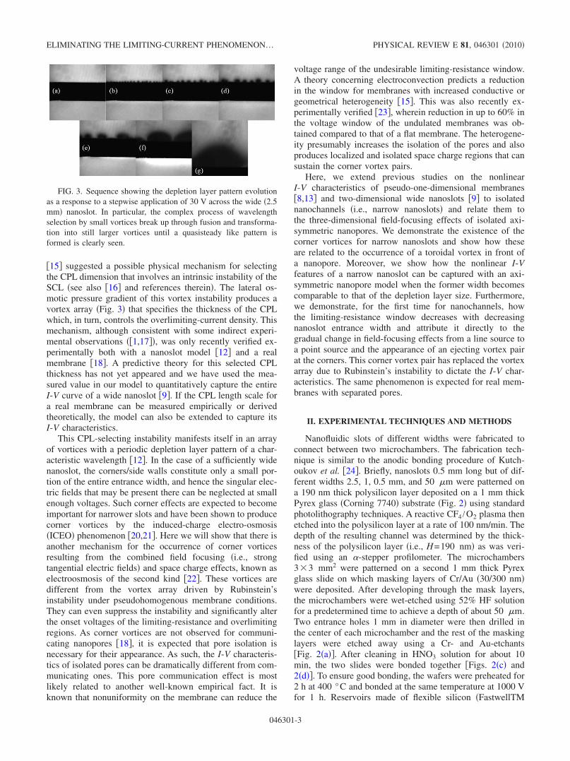
�15� suggested a possible physical mechanism for selectingthe CPL dimension that involves an intrinsic instability of theSCL �see also �16� and references therein�. The lateral os-motic pressure gradient of this vortex instability produces avortex array �Fig. 3� that specifies the thickness of the CPLwhich, in turn, controls the overlimiting-current density. Thismechanism, although consistent with some indirect experi-mental observations ��1,17��, was only recently verified ex-perimentally both with a nanoslot model �12� and a realmembrane �18�. A predictive theory for this selected CPLthickness has not yet appeared and we have used the mea-sured value in our model to quantitatively capture the entireI-V curve of a wide nanoslot �9�. If the CPL length scale fora real membrane can be measured empirically or derivedtheoretically, the model can also be extended to capture itsI-V characteristics.
This CPL-selecting instability manifests itself in an arrayof vortices with a periodic depletion layer pattern of a char-acteristic wavelength �12�. In the case of a sufficiently widenanoslot, the corners/side walls constitute only a small por-tion of the entire entrance width, and hence the singular elec-tric fields that may be present there can be neglected at smallenough voltages. Such corner effects are expected to becomeimportant for narrower slots and have been shown to producecorner vortices by the induced-charge electro-osmosis�ICEO� phenomenon �20,21�. Here we will show that there isanother mechanism for the occurrence of corner vorticesresulting from the combined field focusing �i.e., strongtangential electric fields� and space charge effects, known aselectroosmosis of the second kind �22�. These vortices aredifferent from the vortex array driven by Rubinstein’sinstability under pseudohomogenous membrane conditions.They can even suppress the instability and significantly alterthe onset voltages of the limiting-resistance and overlimitingregions. As corner vortices are not observed for communi-cating nanopores �18�, it is expected that pore isolation isnecessary for their appearance. As such, the I-V characteris-tics of isolated pores can be dramatically different from com-municating ones. This pore communication effect is mostlikely related to another well-known empirical fact. It isknown that nonuniformity on the membrane can reduce the
voltage range of the undesirable limiting-resistance window.A theory concerning electroconvection predicts a reductionin the window for membranes with increased conductive orgeometrical heterogeneity �15�. This was also recently ex-perimentally verified �23�, wherein reduction in up to 60% inthe voltage window of the undulated membranes was ob-tained compared to that of a flat membrane. The heterogene-ity presumably increases the isolation of the pores and alsoproduces localized and isolated space charge regions that cansustain the corner vortex pairs.
Here, we extend previous studies on the nonlinearI-V characteristics of pseudo-one-dimensional membranes�8,13� and two-dimensional wide nanoslots �9� to isolatednanochannels �i.e., narrow nanoslots� and relate them tothe three-dimensional field-focusing effects of isolated axi-symmetric nanopores. We demonstrate the existence of thecorner vortices for narrow nanoslots and show how theseare related to the occurrence of a toroidal vortex in front ofa nanopore. Moreover, we show how the nonlinear I-Vfeatures of a narrow nanoslot can be captured with an axi-symmetric nanopore model when the former width becomescomparable to that of the depletion layer size. Furthermore,we demonstrate, for the first time for nanochannels, howthe limiting-resistance window decreases with decreasingnanoslot entrance width and attribute it directly to thegradual change in field-focusing effects from a line source toa point source and the appearance of an ejecting vortex pairat the corners. This corner vortex pair has replaced the vortexarray due to Rubinstein’s instability to dictate the I-V char-acteristics. The same phenomenon is expected for real mem-branes with separated pores.
II. EXPERIMENTAL TECHNIQUES AND METHODS
Nanofluidic slots of different widths were fabricated toconnect between two microchambers. The fabrication tech-nique is similar to the anodic bonding procedure of Kutch-oukov et al. �24�. Briefly, nanoslots 0.5 mm long but of dif-ferent widths 2.5, 1, 0.5 mm, and 50 �m were patterned ona 190 nm thick polysilicon layer deposited on a 1 mm thickPyrex glass �Corning 7740� substrate �Fig. 2� using standardphotolithography techniques. A reactive CF4 /O2 plasma thenetched into the polysilicon layer at a rate of 100 nm/min. Thedepth of the resulting channel was determined by the thick-ness of the polysilicon layer �i.e., H=190 nm� as was veri-fied using an �-stepper profilometer. The microchambers3�3 mm2 were patterned on a second 1 mm thick Pyrexglass slide on which masking layers of Cr/Au �30/300 nm�were deposited. After developing through the mask layers,the microchambers were wet-etched using 52% HF solutionfor a predetermined time to achieve a depth of about 50 �m.Two entrance holes 1 mm in diameter were then drilled inthe center of each microchamber and the rest of the maskinglayers were etched away using a Cr- and Au-etchants�Fig. 2�a��. After cleaning in HNO3 solution for about 10min, the two slides were bonded together �Figs. 2�c� and2�d��. To ensure good bonding, the wafers were preheated for2 h at 400 °C and bonded at the same temperature at 1000 Vfor 1 h. Reservoirs made of flexible silicon �FastwellTM
FIG. 3. Sequence showing the depletion layer pattern evolutionas a response to a stepwise application of 30 V across the wide �2.5mm� nanoslot. In particular, the complex process of wavelengthselection by small vortices break up through fusion and transforma-tion into still larger vortices until a quasisteady like pattern isformed is clearly seen.
ELIMINATING THE LIMITING-CURRENT PHENOMENON… PHYSICAL REVIEW E 81, 046301 �2010�
046301-3

from Grace bio-Laboratories� were used on top of the open-ings wherein platinum electrodes were introduced. Thenanoslot was filled by introducing distilled, deionized�18 M� cm� water into the large fluidic reservoirs and al-lowing capillary forces to draw the water across the nanoslot.The electrical voltage source and I-V converter �AgilentTechnologies, 4155 B Semiconductor Parameter Analyzer�were connected to the fluidic channel with negligible resis-tive loss via Platinum wires inserted into the reservoirs. Thechannels were cleaned of ionic contaminants using electro-phoretic pumping. The ionic current was observed to decaywhile 10 V were applied across the channels to drive outionic impurities. The reservoirs were periodically flushedwith fresh solution until the current equilibrated to a mini-mum, which typically took �20 min. This procedure wasalso followed by displacing different dilutions of a 1 M po-tassium chloride �KCl� solution to change the ionic strengthand control the degree of EDL overlap.
To obtain the measured I-V curves in Figs. 1 and 4, theapplied voltage was stepped in 0.25 V increments every 3 s,during which time current transients were observed to decaycompletely. In the low concentration limit, the three distinctI-V regimes for the wide nanoslot are indeed observed: alinear Ohmic region, followed by a limiting-resistance regionwith a small slope �large limiting differential resistance� andfinally an overlimiting region �Fig. 1�a��. These data are inqualitative agreement with previous experimentally obtainedI-V curves for true nanoporous membranes ��1�, �17�� andalso for nanochannels �7,9�. It is quite clear that a limiting-resistance region is not discernable for the narrow slots �Fig.4� and there seems to be a direct transition from the Ohmicto the overlimiting region. In the following, we suggest thatthis disappearance of the limiting-resistance region is due tothe severe ionic concentration gradients �resulting, effec-tively, in a much shorter depletion region or CPL� and theejecting vortex pair sustained by enhanced field focusing atthe pointlike narrow nanoslot.
At high enough concentrations ��10−3 M�, only theOhmic region is observed �Fig. 1�a��, irrespective of thenanoslot width. The thinner Debye length stipulates thatEDLs do not overlap within the slot and the nanochannel’sperm-selectivity, space charge, and superior conductivity arelost—it is no longer a model for an ion-selective nanoporousmembrane. Note that the conductance at the low-voltage
Ohmic region does not scale linearly with the ionic strengthat its low values �Fig. 1�b��, suggesting that intraslot resis-tance is important. Ohmic resistance is hence not just due toexternal resistance, as is assumed in earlier theories involv-ing an infinitely conducting membrane �2�. The conductivitywithin the slot is finite and must be considered to quantita-tively capture the true I-V characteristics �9�.
In order to visualize the polarized regions, we usedpositive-charged Rhodamine dye molecules �counterions ofthe nanoslot� at 10 �M concentration. When a large enoughelectric field, beyond the critical voltage for the limiting-
FIG. 5. Confocal image snap-shots of the quasisteady depletion-enrichment layers occurring atthe nanoslot opposite entrancesfor 10−5 M KCl concentrationbuffer at different voltage levelsand nanoslot width: 2.5 mm�a�–�f�, 0.5 mm �g�–�l�, 50 �m�m�–�r�.
FIG. 4. �a� I-V characteristics of nanoslots with varying widthsat 10−5 M KCl concentration; �b� the same data but normalized bythe corresponding conductivity value �Ohmic region�, so as to em-phasize the differences in the limiting-resistance region.
YOSSIFON et al. PHYSICAL REVIEW E 81, 046301 �2010�
046301-4

resistance region, is applied across the nanoslot, an enrich-ment region at the cathodic entrance of the nanoslot is ob-served with high dye concentration while a depletion regionis observed at the anodic side where the dye enters thenanoslot, as seen in Fig. 5 for the nanoslots of differentwidth. Instead of a periodic array of depletion regions ob-served on the anodic side of the wide nanoslot �Fig. 3�, asingle and significantly smaller depletion region is obtainedfor the narrow nanoslot �Figs. 5�n�–5�r��. This is also con-firmed by plotting the selected depletion layer length �de-fined as L in Fig. 5�, which approximates the selected CPLlength scale �12�, for nanoslots of different widths at differ-ent applied voltages �Fig. 6�. At voltages below �5 V fornarrow and �10 V for wide nanoslots �Fig. 6�, it was hardto discern any depletion and the CPL length scales �see alsoFig. 5�. It was hence assumed that the CPL extends all theway to the electrodes ��2.5 mm�, as indicated by the filledsymbols in Fig. 6. The critical voltage in Fig. 6, when theobserved CPL length undergoes a discontinuous drop, is inagreement with the onset voltage of the overlimiting regionin Fig. 4. Beyond this critical voltage, the depletion is clearlydiscernable at the anodic side of the nanoslot interface andbecame more pronounced with voltage. The CPL length in-creased with voltage until it reached again the slot-electrodeseparation. However, compared to conditions below theoverlimiting region, the concentration gradient in the CPL ismuch higher and increases with decreasing slot width. Thatthe ionic concentration gradients in the depletion layer of thenarrower nanoslot are more severe is clearly seen in Fig.7�c�, which compares the concentration profiles of differentslots at 10 V. Figures 7�a� and 7�b� depict the voltage depen-dence of the concentration profile on the applied voltage forthe wide �2.5 mm� and narrow �50 �m� nanoslots, respec-tively. It clearly shows the increase of the total CPL lengthscale in Fig. 6 and also the emergence of the polarized layer�SCL�, with a flattened concentration profile inside the high-gradient depletion region, at higher voltages. These concen-tration plots were extracted from the fluorescent intensityprofile across the depletion region at the anodic side of thenanoslot.
In order to visualize, in a qualitative manner, the innerflow structure of these depletion regions, we used fluorescent
polymer microbeads �Duke Technologies� of 1.2 �m in sizeand 0.02% volumetric concentration, reminiscent of the mi-croparticle imaging velocimetry ��-PIV� technique used forquantitative determination of the velocity field �e.g., �20��. Inthe case of a wide nanoslot �Figs. 8�a�–8�d��, an array ofdepletion regions appear, with each region encompassing asingle vortex pair �12� �see the schematic vortex streamlinesin Fig. 8�c�, and the supplementary video �19��. Individualvortex pairs in the array appear at different locations alongthe nanoslot entrance. The bright spots in Figs. 8�b�–8�d� arethe stagnation points of the different vortex pairs where col-
FIG. 7. Normalized concentration profile of the depletion layerat the anodic side of the �a� wide �2.5 mm� and �b� narrow �50 �m�nanoslots for different applied voltages. The normalized �by thenanoslot length� profile coordinate origin is at the nanoslot entranceat the anodic side and points into the microchamber. Part �c� of thefigure compares the different concentrations profile at 10 V appliedvoltage for the different nanoslot widths, clearly showing increasein concentration gradient with decreasing nanoslot widths.
FIG. 6. The instability selected CPL length scale �L—as mea-sured from Fig. 5� versus the applied voltage for varying nanoslotswidth. Filled symbols stand for cases when there is no observablevortex array �depletion array�. It is then assumed that the depletionlayer extends all the way to the electrodes.
ELIMINATING THE LIMITING-CURRENT PHENOMENON… PHYSICAL REVIEW E 81, 046301 �2010�
046301-5

loids tend to accumulate. They eventually synchronize andcoalesce in a complex manner to create a single �thicker�depletion layer and a single �larger� vortex pair at largeenough voltages �see the transition from Figs. 8�c� and 8�d�and the supplementary video �19��. In contrast, the depletionside of the narrow nanoslot always produces a single vortexpair �Figs. 8�e�–8�k�� at the nano-microchannel junction cor-ners �see the schematic vortex streamlines and the supple-mentary video �19��. Since the colloids mirror the back-ground flow, they follow the closed-streamline patterns ofthe vortex pair and tend to accumulate there. Hence, the ac-cumulation of colloids, as seen also in the stills pictures ofFig. 8, is an indication of the existence of a vortex there.Interestingly, an elevated voltage does not only increase thesize of the depletion region, and its associated vortex pair,but also tilts the vortex pair toward the horizontal plane con-sisting of the nanoslot entrance �compare the schematic vor-tex streamlines of Figs. 8�h� and 8�k��. Furthermore, the vor-tex pair appears at the narrower slots before the emergenceof the depletion layer �see Figs. 8�e� and 8�f� and the supple-mentary video �19��. This suggests that the single vortex pairof the narrow slots originates from a mechanism differentfrom the initial vortex array in the wider slots. The latter ismost likely due to the SCL instability ��15,12,18�� but thedominant corner effects of the former suggests that cornerpolarization �e.g., ICEO �20,21�� at low voltages and spacecharge emergence concurrent with large tangential electricfield component �22� �due to the field-focusing geometry� athigher voltages ��10 V� are responsible for the vortex pairgeneration of narrow slots. This vortex pair enhances theionic current through the nanoslot �as seen in Fig. 4�b��, asits mixing action reduces the selected CPL length scale �12�.
For a sufficiently large depletion layer length relative tothe nanoslot width, the three-dimensional field-focusing re-sults in an almost spherically shaped depletion layer. Moreprecisely, for the fabricated narrow nanoslot �Fig. 9�a��, it is
a quarter of a sphere as the bottom surface of the chip be-haves as a symmetry plane. This observation allows us toproduce a simple model that connects the narrow nanoslot tothe nanopore. Both share the same field-focusing behavior,but with different radial geometries, and the quarter-spheredepleted region of the nanoslot is exactly one half of thehalf-sphere region in front of the nanopore �Fig. 9�b��.
We find the thickness of the depletion layer at one en-trance to be comparable to that in the enrichment region inthe other. However, due to the low ionic strength in thedepletion layer, it is quite obvious that it is the depletionlayer that controls the current and the thickness of both lay-ers. The vortices and the resulting constrained depletionlayer only appear beyond a critical voltage of about 10 V�Figs. 8�c� and 6� and 5 V �Figs. 8�e� and 6� for the wide andnarrow nanoslots, respectively. Below this voltage, the CPLextends to the electrode and beyond it the vortex pair selectsa smaller CPL dimension that increases monotonically withvoltage, as shown in Figs. 6 and 8.
III. THEORETICAL MODEL
A nonideal permselective membrane necessitates a modelfor membranes of finite conductance and a theory thatcouples all three domains of the problem �i.e., both the CPLsat the anodic and cathodic sides of the membrane, and thenanopore�. We employ Manazanares et al.’s simplified model�14� for a nonideally permselective nanoporous membrane,in which the surface charge is included in the averaging ofthe ion transport and Poisson equations across both solid andliquid phases to produce an effective homogeneous model.The membrane is assumed to contain fixed charged groups ata uniform volumetric concentration density �. This approachwas previously used for the case of a wide nanoslot �9�, buthere it is extended to the axisymmetric nanopore geometry�Fig. 9�b�� with matching conditions at the entrance to cap-
FIG. 8. �Color online� Similarly to Fig.5—confocal image snapshots were taken of thequasisteady depletion layer occurring at the an-odic entrance of the widest �a�–�d� and narrowest�50 �m� �e�–�k� nanoslots at varying appliedvoltages. However, in addition to the Rhodaminedye molecules, fluorescently tagged 1.2 �m�0.02% volumetric concentration� were added tothe electrolyte solution �10−5 M KCl� in order tovisualize the flow dynamics, and in particular, theresulting vortex pairs �sketched schematicallybased on the supplementary videos �19��. In con-trast to the narrow nanoslot case, wherein only asingle pair of vortex can be observed, multiplevortex pairs are observed in the wide nanoslotcase before they merge into a single large vortexpair �d� for large enough voltages.
YOSSIFON et al. PHYSICAL REVIEW E 81, 046301 �2010�
046301-6

ture the field-focusing effect in the bounding reservoirs �mi-crochambers� that arises from the three-dimensionality of thenanopore. The same field-focusing effect also occurs for truemembranes consisting of widely separated nanopores but hasyet to be scrutinized.
Figure 9�b� depicts schematically the two-sided axisym-metric micro-nanopore junction problem geometry viewed inprofile. We use a spherical coordinate system �R� in the mi-croreservoirs and a Cartesian coordinate system �x� insidethe intra-nanopore. The three-dimensional problem can befurther simplified into an effective one-dimensional problem,by assuming radial symmetry in the microchamber regionsand treating only axial changes within the nanopore region.This assumption is valid because the nanopore radius, h, ismuch smaller than the dimensions of the microreservoir.
In the Ohmic region wherein the nanopore/nanoslot resis-tance dominates over that of the microreservoirs, it is onlythe former parameters �i.e., cross-section area, A, length, d,and volumetric fixed charge density �� that control the con-ductance of the entire system. The parameter � depends onthe nanopore radius h �or nanoslot height, H� and the surfacecharge density. The latter, unless chemically modified, isusually predetermined by the surface chemistry of the fabri-
cation process. Hence, for the same �, the nanopore �Fig.9�b�� and nanoslot �Fig. 9�a�� conductance are related to eachother by the ratio of the nanopore ��h2� to nanoslot �wH�cross-section area. As for microfabricated nanoslot w�H ,h,this ratio is �h /w1.
In the non-Ohmic regions �i.e., limiting-resistance andoverlimiting regions� the differential resistance is determinedmainly by processes occurring outside the nanochannel/nanopore. A narrow nanoslot of width that is much smallerthan the depletion layer length �i.e., wL� can be effectivelydescribed as a point source/sink in terms of the field-focusingeffect as in the case of a nanopore. Hence, for large enoughdepletion length, the nanoslot and nanopore non-Ohmic dif-ferential resistances are again related by the ratio of theircross-section area. It is obvious that a narrow nanoslot�i.e., wL� cannot be modeled anymore by the two-dimensional approach which is only applicable for widenanoslots �i.e., w�L� �9�. Instead, the three-dimensionalfield-focusing effect can be captured by the more simplifiedaxisymmetric nanopore geometry as described in thefollowing.
Both the enrichment region and the depletion region inthe two entrances are assigned the CPL length L. By appro-priate coordinate transformation �i.e., x=−R at −L�x�−h,and x=d+R at d+h�x�d+L, where L is the CPL lengthand d is the nanopore length� we can describe all three do-mains in terms of one axial coordinate x. We chose the fol-lowing normalization for the axial coordinate x=Lx, ionicconcentration c=c0c, electric potential �= �RT /zF��, ionic
flux j= �Dc0 /L�j and electric current density i= �FzDc0 /L�i.Here, the tilda stands for dimensional parameters, c0 is thebuffer solution concentration, F denotes the Faraday number,z the ion valency, R the universal gas constant, T the absolutetemperature, and D the ionic diffusion coefficient. We alsodefine the nondimensional parameter =� /L as the ratio be-tween the EDL length scale, � �=���0� fRT /2z2F2c and theCPL length L. Herein, �0 is the electric permittivity ofvacuum and � f denotes the dielectric constant of the electro-lyte solution.
As is true for most micro- and nanochannel dimensionsand applied voltages, convection effects can be discarded�i.e., negligible Peclet number�. A symmetric electrolyte�z+=−z−=z� of equal diffusivities �D+=D−=D� is assumedto simplify the analysis. Thus, � and c� satisfy the follow-ing �Nernst-Planck� equations for the ionic species in thethree domains, with radial symmetry invoked in the mi-croreservoirs,
�c�
�t=��
�
�x+
2
x� �c�
�x� c���
�x at − 1 � x � −
h
L
�
�x� �c�
�x� c���
�x at −
h
L� x �
d + h
L
� �
�x+
2
x − d/L� �c�
�x� c���
�x at
d + h
L� x �
d + L
L
, �1�
FIG. 9. �Color online� Schematic description of the three-dimensional �a� narrow nanoslot geometry and �b� axisymmetrictwo-sided micro-nanopore junction. When the depletion region ex-tent L is much larger than that of the nanoslot width w, the field-focusing effect at the nanoslot resembles that of the nanopore. How-ever, instead of the depletion region being half a sphere, it is aquarter of a sphere in the former case.
ELIMINATING THE LIMITING-CURRENT PHENOMENON… PHYSICAL REVIEW E 81, 046301 �2010�
046301-7

and the corresponding Poisson’s equation for the three domains are
�1
x2
�
�x�x2��
�x = −
c+ − c−
2 2 at − 1 � x � −h
L
�2�
�x2 = −c+ − c− − �
2 2 at −h
L� x �
d + h
L
1
�x − d/L�2
�
�x��x −
d
L2��
�x� = −
c+ − c−
2 2 atd + h
L� x �
d + L
L
, �2�
where � is the effective fixed volumetric charge �normalizedby c0� from surface charge that allows a one-dimensionalformulation within the nanopore �14�. At the interfacebetween the diffusion layer and the Ohmic bulk
solution �i.e., R=L� � and c� satisfy the electrostaticconditions
��/�x = − I/4� at x = − 1��I� , �3a�
� = 0 at x = 1 + d/L��II� , �3b�
and the equality of the ionic concentrations to that of thebuffer solution concentration c0
c� = 1 at x = − 1��I�, x = 1 + d/L��II� . �4�
In Eq. �3� I is the imposed electric current through �I whichis positive in the positive x direction. Furthermore, for futurereference, the electric potential drop across the system �i.e.,between �I and �II� is designated as V.
At the interface between the nano- and microchannels
�i.e., R=h� we impose the matching conditions of electricfield E and ionic flux j� continuity to capture the field andflux focusing effects,
�E�R = �E�x/2�j��R = �j��x/2
� at x = − h/L�SI�, x = d/L + h/L�SII� .
�5�
IV. FIELD-FOCUSING EFFECT
An analog of Levich’s limiting-current density can betheoretically estimated for this geometry by including in-traslot resistance and geometric field-focusing effects, as afirst-order approximation of the limiting-resistance region inFigs. 1�a� and 4�a�. This limiting current occurs when theionic concentration at the anodic nanopore-electrolyte inter-face �x=−h /L� vanishes when the electroneutrality condition�c+=c−=c� is employed to describe the ionic transport withinthe diffusion layer. Hence, the resulting ionic fluxes at theanodic side of the nanopore are
j� = − � �c
�x� c
��
�x , �6�
wherein j� is positive in the positive x direction, from whichone obtains for the spherical geometry outside the nanopore
�c
�x= −
j+ + j−
2= −
J+ + J−
4�x2 , �7�
wherein J�=2�x2j� is the steady ionic flux �positive in thepositive x direction� through the surface of half a sphere ofR=−x and the x term in the denominator on the right cap-tures the field and flux focusing effects of the spherical ge-ometry.
Combining Eqs. �7� and �4� yields the following nonlinearconcentration profile in the DL �see Fig. 10�a��:
c = 1 +J+ + J−
4��1 +
1
x at − 1 � x � − h/L , �8�
and that of the electric potential
FIG. 10. Analytical results for the limiting-current conditionsdepicting the: �a� concentration and �b� potential profiles at the an-odic side of a pseudo-one-dimensional membrane, two-dimensionalnanoslot, and three-dimensional nanopore, exhibiting an increasingfield-focusing effect.
YOSSIFON et al. PHYSICAL REVIEW E 81, 046301 �2010�
046301-8

� = ln�1 +J+ + J−
4��1 +
1
x��� + 1
� − 1 at − 1 � x � − h/L .
�9�
Imposing the limiting-current condition c=0 at x=−h /L �SI�on Eq. �8� yields J++J−=4��h /L� / �1−h /L�. The sphericalgeometry that focuses the field into the nanopore is respon-sible for a large reduction in the current corresponding to theratio of the nanopore radius to the diffusion layer thickness,h /L, which is typically on the order of 10−4. This electriccurrent I=J+−J− results in the following expression for thelimiting current �normalized by FzDc0L�
IL = 4�� h/L1 − h/L�� + 1
� − 1 , �10�
wherein �=−J+ /J− is the ratio between the counter- and co-ions fluxes �assuming that the nanopore surface is negativelycharged� and is related to the permselectivity of the nano-pore. For an ideal permselective nanopore �i.e., �→�� weobtain IL ��→�=4��h /L / �1−h /L��. Following Manazanareset al. �14� �Eq. �16�� � is related to � through the ratio of thecounter- to co-ions concentration within the membrane�=c+��� /c−��� at −h /L�x�d /L+h /L, wherein explicitexpressions for c���� are given in Eq. �17�. It is obviousfrom Eq. �2� that within the membrane nanopore this ratioincreases with �. Also, from Eq. �10� it is clear that thenormalized limiting-current IL monotonically increases as thepermselectivity degree � decreases.
In contrast, for the pseudo-two-dimensional wide nanoslotcase studied in �9�, the nonlinear concentration and potentialprofiles in the DL are
c = 1 +J+ + J−
�ln�− x� at − 1 � x � − H/L , �11�
� = ln�1 +J+ + J−
�ln�− x���� + 1
� − 1 at − 1 � x � − H/L ,
�12�
while the limiting current �normalized by FzDc0� is
IL = −�
ln�H/L��� + 1
� − 1 . �13�
For the pseudo-one-dimensional membrane ��9,14�� the fa-miliar linear concentration profile and potential profile in theDL is
c = 1 −J+ + J−
2�x + 1� at − 1 � x � 0, �14�
� = ln��1 −J+ + J−
2�x + 1��� + 1
� − 1� at − 1 � x � 0,
�15�
while the limiting-current density �normalized by FzDc0 /L�is
IL = 2�� + 1
� − 1 , �16�
with the familiar asymptotic limit of IL=2 for an ideal perm-selective membrane ��→�� �e.g., �13��. The extra algebraicterm in the nanopore case in Eq. �10� and the logarithmgeometric term in the nanoslot case in Eq. �13� are due to thefield-focusing effects of the two different geometries. It isclear that both serve to lower the limiting-current density butthe difference is more pronounced for the nanopore.
However, the limiting-current density in Eq. �10� onlyestimates the current density at the limiting-resistanceregion and not its differential resistance. The dominance ofintraslot resistance occurs because of field focusing into thenanopore—all the current must go through the nanopore andthe converging field produces a high current density from thebulk in Eq. �10� that increases with the large ratio of the CPLthickness to the nanochannel height. To sustain this highOhmic current from the bulk, a polarized layer develops asthe bulk concentration at the interface approaches zero tointroduce a larger field for flux into the pore �8�. With theappearance of the polarized layer, the electroneutral assump-tion of the limiting-current theory breaks down and a finitedifferential resistance develops at the anodic CPL.
The development of the polarized region can be capturednumerically using the above pseudo-one-dimensional formu-lation �1�, �2�, �3a�, �3b�, �4�, and �5�. The distinct DC iondistributions and I-V characteristics in the Ohmic andoverlimiting-current regimes are demonstrated for the axi-symmetric geometry of a nanopore in Fig. 11. All computa-tions are done with one specific CPL thickness L. Note thatthe depletion side on the left, where the bulk concentration capproaches zero, controls the I-V characteristics and containssignificant space charge in its EPL. The enrichment side onthe right with an ionic concentration higher than the bulk isalways electroneutral �outside the thin equilibrium EDL�without a polarized layer. It is this polarized layer, amplifiedby the field-focusing effect, on the depletion side that invali-dates the classical limiting-current theory involving onlyelectroneutral bulk transport.
The varying field-focusing intensities in terms of the ionicconcentration and potential profiles on the anodic side ofthe membrane/nanoslot/nanopore are depicted in Figs. 10�a�and 10�b�, respectively. It is quite clear that when shiftingfrom a pseudo-one-dimensional to a three-dimensional field-focusing geometry, the gradients near the nanochannel inter-face becomes more severe, resulting in most of the ionicconcentration and potential drop to occur there. Hence, forthe pseudohomogenous membrane case, it is the vortex in-stability that is responsible for selecting a much smaller CPLlength scale �which otherwise goes all the way to the elec-trode�. However, in the nanopore case, it is the geometricalthree-dimensional field-focusing effect that effectively dic-tates a significantly smaller CPL, which is weakly dependenton the nanoslot-electrode distance. For nanopores, the role ofthe corner vortices in sustaining this small CPL length scaleis probably not as significant as that of the vortex instabilityarray in the former case.
ELIMINATING THE LIMITING-CURRENT PHENOMENON… PHYSICAL REVIEW E 81, 046301 �2010�
046301-9

V. OHMIC REGION OF THE I-V CURVE
From the insets of Figs. 11�a� and 11�b�, it is clear that theresistance is negligible in the cathodic enrichment side andthe intraslot and CPL layer resistance on the anodic depletionside control the ion current flux. The anodic CPL resistanceis further broken down into two parts: SCL and DL. As isevident in Fig. 11�a� and inset of Fig. 11�c�, the SCL layerdoes not exist in the Ohmic region of the I-V curve. Withfield focusing, nanoslot/nanopore resistance dominates overDL resistance in the Ohmic region as seen in the inset of Fig.11�a�. As the conductance of the nanoslot in the low concen-tration limit is specified by the total surface charge, the re-sistance in this region has a very different dependence on theionic strength for a slot whose height is much larger than theDebye layer �Fig. 1�b��.
We analyze the Ohmic region of the nanoslot data in Fig.1�a� to obtain the surface charge density in the form of � inthe model of Eq. �2�. The DC conductance was determinedby fitting the slope of the ionic current as a function ofthe applied voltage �Fig. 1�a��. At high c0, where �H�1
��=�−1�, the conductance I / V=2zF�c0wH /d is linear withc0, as is consistent with bulk electrolyte conductance. At lowc0, where �H1 and the surface charge density is2����zFc0H, the conductance is independent of H and c0,
behaving as I / V�2����w /d �wherein �=zF�=zFD / �RT� isthe ion mobility, w is the nanoslot width, d is the nanochan-nel length and the factor 2 stands for both the top and bottomwalls of the nanoslot while the side walls are neglected�. Theconstant conductance reflects the fact that the nanoslot ionsare mostly counterions and, due to electroneutrality, theirnumber is equal to the total surface charge independent ofbulk ionic strength or slot height. As is consistent with ourmodel, conductance enhancement due to electro-osmosis hasbeen neglected. For the nanoslot parameters �Fig. 9�a��H�200 nm, d=500 �m, w=2 mm, and KCl solution pa-rameters z=1, �=7.6�10−8 m2 /V s �25�, a fitted value of���=7 mC /m2 for the surface charge density �inside themeasured surface charge density range of 2–100 mC /m2
reported in �26� for similar substrates� was obtained from thelow c0 data of Fig. 1.
Following Manazanares et al. �14�, we substitute the sur-face charge density, �, by a fixed volume charge density
zF�=−2� /H for the nanoslot case of about 74 KC /m3.Based on the well-known Donnan equilibrium relations �14�,the ionic concentrations within the nanoslot can be expressedas
c� = � �/2 + ���/2�2 + c02 at 0 x d . �17�
This produces a universal ionic conductance �27� for the in-traslot dominating Ohmic region,
I/V = �F2�zi2�ici�wH/d = 2F����/2�2 + c0
2wH/d , �18�
which reduces to I / V=2zF�c0wH /d in the limit of high con-
centrations, c0��, and to I / V�zF�c+wH /d=−2��w /d in
the limit of low concentrations, c0�. As seen in Fig. 1�b�,a good agreement is obtained between the model �18� �thinblack continuous line� and the experimentally measuredOhmic data. Also depicted in Fig. 1�b� is the expected bulkconductance �thin black dashed line� as obtained from model�18� while neglecting the effect of the nanochannel surface
charge, i.e., �=0. A clear deviation from this bulk con-ductance is clearly seen to occur at concentrations of about1 mM, indicating that ion permselective effects becomedominant at ionic strengths below this value.
Applying the model �1�, �2�, �3a�, �3b�, �4�, and �5� of anaxisymmetric nanopore to the narrow nanoslot requires tosomewhat relate between the two different geometries, thatmainly differ by the large ratio of cross-section areas, as thelength, d, may be of the same order. Taking the nanopore
model to have the same parameters d, �, and � as those ofthe narrow nanoslot chip, dictates the nanopore radius h to be
according to the relation zF�=−2� /h. Hence, according toEq. �18�, the nanoslot and nanopore Ohmic conductance arerelated by a factor of cross-section area ratio �wH /�h2�.
FIG. 11. Numerical computation results forthe concentration-polarization profiles across anaxisymmetric nanopore �0x1� for currentsbelow �a� and beyond �b� the limiting-current IL.The insets of parts �a� and �b� of the figure de-scribe the potential drop across the system. Part�c� of the figure depicts the ion concentration pro-files on the anodic side of the nanopore for theoverlimiting conditions of �b�, exhibiting an SCL,in contrast to the profile of �a� in the inset. Alsodepicted are the electroneutral DL and the EDL.The I-V curve for the membrane, exhibiting aninflection point at IL, is shown in �d� with theconditions for �a� and �b� indicated. The normal-ized values of �=2, d=1, h /L=10−2, and =10−3 have been used.
YOSSIFON et al. PHYSICAL REVIEW E 81, 046301 �2010�
046301-10

VI. NON-OHMIC REGIONS OF THE I-V CURVE
In contrast to the Ohmic region, wherein the field-focusing effect is of no importance at all since it is only thenanochannel part that controls the current, the non-Ohmicregion current strongly depends on the degree of field focus-ing at the channel entrance. This understanding combinedwith the mechanism of selecting the diffusion layer �CPL�length scale was recently used by us �9� to provide the firstcomprehensive quantitative explanation of the nonlinear I-Vcurve consisting of the three distinct regions �Ohmic, limit-ing resistance and overlimiting� for the wide nanoslot case.The same approach, but this time using the three-dimensional field-focusing model �1�, �2�, �3a�, �3b�, �4�, and�5� in Sec. III, can be applied for the narrow nanoslot dataof Fig. 4.
In contrast to the wide nanoslot case with a very widevoltage window for the limiting-resistance region �Fig. 4�bounded between the linear Ohmic and overlimiting regions,the narrow nanoslot does not exhibit a discernable limiting-resistance region. It is quite obvious that with decrease of thenanoslot width, the system nonuniformity increases, asboundary effects associated with the nanoslot sidewalls be-comes more pronounce. One obvious consequence of thisnonuniformity is the emergence of corner vortices �Figs.8�e�–8�k�� that are quite distinct from Rubinstein’s vortexarray instability away from the corners �15�. This suggeststhat the vanishing of the limiting-resistance region is inti-mately connected to increase of the system nonuniformity.
For channels without permselectivity or an extended po-larized layer, corner vortices are attributed to induced-chargepolarization of the corners �20,21� when charge build-up atthe corners produces a large converging flow. In the currentcase of the nanopores, a localized space charge region existsat the pore entrance and the focusing field toward the pore�i.e., non-negligible tangential field component� can impart aconverging �toward the nanopore entrance� Maxwell bodyforce on the liquid at the space charge region �22�. Sincethe similitude between the electric and velocity fields �28�breaks, once the extended polarized layer kicks in, and
hence, also the fluid irrotational behavior, flux continuity ar-guments dictates that the excess flux at the microchamberside �over that through the nanopore� produce a vortex simi-lar to the one seen in �20,21�.
The finite element based numerical simulation resultsshown in Fig. 12 indeed predict such a vortex �actually, atorus with an axis corresponding to the axial coordinate� toappear at the depletion layer side of the axisymmetric nano-pore wherein an extended polarized layer can be sustained.In the case of a planar nanochannel, it is a vortex pair thatemerges from the corners. The full set of nonlinear coupledequations: Poisson’s, continuity of ions �Nernst-Planck� andStokes equations,
�2� = −zF�c+ − c−�
�0� f, �19a�
� · �− D � c� �DzF
RTc� � � = 0, �19b�
���2u − �p − zF�c+ − c−� � � = 0, � · u = 0,
�19c�
assuming a small Peclet number �hence, decoupling betweenthe electrostatic and hydrodynamic problems�, was solvednumerically for the axisymmetric geometry depicted in Fig.12�a� consisting of a nanopore connecting two opposite mi-croreservoirs. Herein, u is the velocity vector, �� is the dy-namic fluid viscosity and p is the hydrodynamic pressure.Far field conditions included an applied potential difference,bulk ionic concentration and zero pressure difference. At thewalls, an equilibrium surface charge density was taken, to-gether with the ion impermeability and the no-slip boundaryconditions.
The resulting toroidal vortex has a direction of rotationthat is in agreement to that observed experimentally �com-pare Fig. 12 with Fig. 8�k��. We note that the focusing tan-gential field in the direction of the flow can be screened byneighboring pores and hence the onset of these ejecting vor-
FIG. 12. �Color online� �a� Finite-elementnumerical simulation of the electrokinetic flowfor an axisymmetric nanopore system boundedby two microreservoirs �continuous lines—streamlines; surface plot—normalized co-ionsconcentration�. Note the enrichment-depletion ofthe co-ions at the cathodic/anodic entrances, re-spectively. �b� Close up of the anodic side show-ing that the direction of the vortex rotation is op-posite from that predicted for Rubinstein’sinstability vortex pair �15�. �continuous lines—streamlines; vectors—velocity field; surfaceplot—normalized net ionic charge density�.
ELIMINATING THE LIMITING-CURRENT PHENOMENON… PHYSICAL REVIEW E 81, 046301 �2010�
046301-11

tices should be a function of the pore separation. In contrast,the wide slot has an extended space charge region in thelateral direction and the same mechanism would have pro-duced a single vortex cylinder with a vorticity direction or-thogonal to the observed ones. The vortex array for the wideslot due to Rubinstein’s instability, on the other hand, has avorticity vector that is antiparallel to the observed one and isnot due to boundary effect. This suggests that the ejectingvortex torus is unique to the narrow pore and, unlike aninstability, it exists for all voltages beyond the threshold volt-age of the Ohmic to limiting-resistance transition associatedwith the occurrence of SCL. This is consistent with the early�Fig. 8�f�� detectable occurrence of the vortex pair for narrowslots and its absence of a limiting-resistance region, whichproduces a direct transition from Ohmic to overlimiting re-gions.
This observation of vanishing limiting-resistance region isincorporated in the theoretical model of the nanopore �nar-row nanoslot� wherein the critical voltage for the overlimit-ing region is shifted to coincide that of the threshold voltagedue to the development of the SCL, as the controlling resis-tance switches from the intraslot region �Ohmic� to the po-
larized layer region �limiting resistance�. This threshold volt-age is estimated from the dimensional versions of thelimiting-current Eq. �10� and the nanopore conductance �18�as
V0 = 2zDc0L� h/L1 − h/L�� + 1
� − 1�����/2�2 + c0
2h2/d�−1.
�20�
As most of the voltage drop shifts from the intraslot to theexternal polarized layer, when an Ohmic to overlimiting-current transition occurs, this suggests that the nanoslot en-trance geometrical properties become much more importantthan its length d. Hence, the appropriate translation betweenthe narrow nanoslot and the nanopore overlimiting conduc-tance is the ratio of the cross-section areas, in contrast to theOhmic case in which it is the ratio of the cross-section areadivided by the channel length �A /d, see Eq. �18��.
VII. CONCLUDING REMARKS
Thus, using different geometrical models we have shownexperimentally and theoretically �Fig. 10� that, due to the
FIG. 13. �a� Normalized �by IL of Eq. �16��current versus the normalized �by V0 of Eq. �20��applied voltage for identical number of nanoporesin either isolated �with field focusing� or commu-nicating �i.e., nanoporous membrane, w/o fieldfocusing� mode. The overlimiting resistance isapproximated as equal to that of the Ohmic re-gion. An arbitrary voltage window of 2V0 is takenfor the limiting-resistance region of a nanoporousmembrane. This conceptual figure should becompared to the experimental data of Fig. 4�b�;�b� Normalized current versus the normalized �bythe selected CPL length L� pore-pore separationdistance s for the case of isolated and communi-cating nanopores, as obtained from part �a� of thefigure, for the particular case of V /V0=3. A clearlocal maximum of the current is seen around thetransition value of s /L=1.
YOSSIFON et al. PHYSICAL REVIEW E 81, 046301 �2010�
046301-12

enhanced field-focusing effect of a pointlike nanopore, theconcentration-polarization �and potential� gradients becomemore severe with decreasing nanoslot entrance width. One ofthe consequences of the isolation is a single localized deple-tion region in the narrow nanoslot case, instead of an array ofthem in the wide nanoslot case due to an instability. Thisisolated space charge region at the pore entrance produces anejecting vortex pair for isolated narrow nanochannels �Fig. 8�or a vortex toroid for isolated nanopores �Fig. 12�. Animportant consequence is the vanishing of the limiting-resistance window in the narrow nanoslot �Fig. 4� in contrastto a very clear region in the wide nanoslot case, thus produc-ing very high current density for all voltages that are notlimited by Levich’s diffusion-limited current �2�. By usingvarying nanoslot widths, we were actually able to capture thegradual vanishing of the limiting-resistance window with de-creasing width �Fig. 4�.
An intriguing question is when the nanopores of a nano-porous membrane are effectively isolated and exhibit point-like field-focusing effect studied here. From our analysis, thedepletion layer at the limiting-current of an isolated nano-pore extends to �0.1L �contains 99% of the concentrationdrop. See Figs. 10, 3D� and hence a good estimate would bethat this is the minimum pore separation to eliminate pore-pore interaction �29,30�. Since the current scales linearly
with the total pores area, for a fixed pore radius, the currentis inverse proportional to the quadrate of the pore-pore sepa-ration length. Thus, taking the 1D membrane limiting currentas a measure of the current for pore separations smaller thanthe depletion layer length, and the Ohmic-like behavior ofisolated nanopore as a measure of the overlimiting current�approximating the overlimiting differential resistance as thatin the true Ohmic region �18�—see Fig. 4� for pore separa-tions larger than the depletion layer �see Fig. 13�a��, we ob-tain Fig. 13�b�. As seen, a maximum of the current occurs atan optimal pore separation �s� when it is roughly the deple-tion layer length �L�. Although this is a sharp maximum, it isa local one as the current is higher for s /L less than 0.6.However, while small pore separations would obviously pro-duce a larger current due to area considerations, they maycorrespond to mechanically unstable membranes that are dif-ficult to fabricate.
ACKNOWLEDGMENTS
G.Y. was supported by the Taub Foundations. H.C.C.acknowledges support from NSF-IDBR under Grant No.0852741. We are grateful to Prof. Y. Zhu and Prof. A. Sea-baugh of Notre Dame for the use of their equipment and fortheir advice.
�1� F. Maletzki, H.-W. Rosler, and E. Staude, J. Membr. Sci. 71,105 �1992�.
�2� V. G. Levich, Physicochemical Hydrodynamics �Prentice-Hall,New York, 1962�.
�3� D. Stein, M. Kruithof, and C. Dekker, Phys. Rev. Lett. 93,035901 �2004�.
�4� Q. Pu, J. Yun, H. Temkin, and S. Liu, Nano Lett. 4, 1099�2004�.
�5� A. Plecis, R. B. Schoch, and P. Renaud, Nano Lett. 5, 1147�2005�.
�6� R. Karnik, C. Duan, K. Castelino, H. Daiguji, and A. Majum-dar, Nano Lett. 7, 547 �2007�.
�7� S. J. Kim, Y. C. Wang, J. H. Lee, H. Jang, and J. Han, Phys.Rev. Lett. 99, 044501 �2007�.
�8� I. Rubinstein and L. Shtilman, J. Chem. Soc., Faraday Trans. 275, 231 �1979�.
�9� G. Yossifon, P. Mushenheim, Y. C. Chang, and H.-C. Chang,Phys. Rev. E 79, 046305 �2009�.
�10� H. Bayley and P. S. Cremer, Nature �London� 413, 226 �2001�.�11� J. Li, D. Stein, C. McMullan, D. Branton, M. J. Aziz, and J. A.
Golovchenko, Nature �London� 412, 166 �2001�.�12� G. Yossifon and H.-C. Chang, Phys. Rev. Lett. 101, 254501
�2008�.�13� Y. Ben and H.-C. Chang, J. Fluid Mech. 461, 229 �2002�.�14� J. A. Manzanares, W. D. Murphy, S. Mafe, and H. Reiss, J.
Phys. Chem. 97, 8524 �1993�.�15� I. Rubinstein and B. Zaltzman, Phys. Rev. E 62, 2238 �2000�.�16� B. Zaltzman and I. Rubinstein, J. Fluid Mech. 579, 173
�2007�.�17� I. Rubinshtein, B. Zaltzman, J. Pretz, and C. Linder, Russ. J.
Electrochem. 38, 853 �2002�.�18� S. M. Rubinstein, G. Manukyan, A. Staicu, I. Rubinstein, B.
Zaltzman, R. G. H. Lammertink, F. Mugele, and M. Wessling,Phys. Rev. Lett. 101, 236101 �2008�.
�19� See supplementary material at http://link.aps.org/supplemental/10.1103/PhysRevE.81.046301 for supplementary videos.
�20� Y. Eckstein, G. Yossifon, A. Seifert, and T. Miloh, J. ColloidInterface Sci. 338, 243 �2009�.
�21� S. K. Thamida and H.-C. Chang, Phys. Fluids 14, 4315�2002�; G. Yossifon, I. Frankel, and T. Miloh, ibid. 18, 117108�2006�.
�22� S. S. Dukhin, Adv. Colloid Interface Sci. 35, 173 �1991�.�23� J. Balster, M. H. Yildirim, D. F. Stamatialis, R. Ibanez, R. G.
H. Lammertink, V. Jordan, and M. Wessling, J. Phys. Chem. B111, 2152 �2007�.
�24� V. G. Kutchoukov, F. Laugere, W. van der Vlist, L. Pakula, Y.Garini, and A. Bossche, Sens. Actuators, A 114, 521 �2004�.
�25� CRC Handbook of Chemistry and Physics, 63rd ed., edited byR. C. Weast �CRC Press, Boca Raton, 1982�.
�26� R. Karnik, R. Fan, M. Yue, D. Li, P. Yang, and A. Majumdar,Nano Lett. 5, 943 �2005�.
�27� R. F. Probstein, Physicochemical Hydrodynamics—An Intro-duction �Butterworths, Boston, 1989�.
�28� E. Cummings, S. Griffiths, R. Nilson, and P. Paul, Anal. Chem.72, 2526 �2000�.
�29� G. Yossifon, Y. C. Chang, and H.-C. Chang, Phys. Rev. Lett.103, 154502 �2009�.
�30� H.-C. Chang and G. Yossifon, Biomicrofluidics 3, 012001�2009�.
ELIMINATING THE LIMITING-CURRENT PHENOMENON… PHYSICAL REVIEW E 81, 046301 �2010�
046301-13