Embed Size (px)
Citation preview
1
EM Simulation using Sonnet Lite
Part 1: Design of Patch Antennas using the free Sonnet Lite-Version 12.53 (http://www.sonnetsoftware.com)
Version 1.1 Copyright by Gunthard Kraus, Elektronikschule Tettnang, Germany Guest Lecturer at the Duale Hochschule Baden Württemberg (DHBW), Friedrichshafen, Germany Email: [email protected] Homepage: www.gunthard-kraus.de
April 1st, 2011
2
Contents Page 1. Introduction 3 2. Installation and Licensing 3 3. First Project: 8 GHz – Patch Antenna with Microstrip Matching 4
3.1. Applications 4 3.2. Preparations 4 3.3. Design Procedure 6 3.4. First Simulation using Sonnet Lite 7
3.4.1. Preliminary Work 7 3.4.2. Simulation and Simulation Results 15 3.4.3. Calculation of the Antenna Radiation Resistance 17
3.5. Matching to 50Ω 18 3.5.1. Matching by a λ/4 – Transmission Line 18
3.5.2. Reasons for the Resonating Frequency Deviation 21 3.5.3. Optimizing 23 3.5.4. Determination of 3dB- Power-Bandwidth 25
3.6. View the Current Density on the Patch 26
4. New Version: Feeding from the Backside 28

3
1. Introduction SONNET is an EM simulator (using the method of moments) for every kind of planar structures like microstrip , stripline or coplanar circuits (= couplers, matching lines, filters, gaps, stubs, patch antennas…). But if you are only familiar with SPICE or S – Parameter simulation, you’ll get problems: EM simulation is something completely different!. At first the structure must be divided in a huge collection of little “cells”. The properties of each cell are then analyzed and computed by the software and at last the sum of all cell properties is found by integration. Therefore Sonnet uses a rectangular „box“ consisting of four walls (material = lossless = with infinite conductivity), but bottom and top material can be defined by the user. So a lot of settings is necessary.
Using lossless material for the wall means that they now act as „mirrors“ for the fields in the box. But this fact is not necessary for bottom and top: e. g. when simulating an antenna structure the radiated energy must have a chance to escape out of the box! So you have different material options like „lossless“ or „wave guide load“ or „free space“ or a material due to your choice from a list in the library (e. g. copper or gold). The field distribution in such a box is well known and thus the simulation and calculation gives a high precision (when using very, very small cells). But simulating with small cells results also in long computing times and big result data files…and this is the only serious problem for the Snnet Lite user with its memory, restricted to 16 MB! So as a Sonnet Lite user you can expect a simulation accuracy between 1% and 5%. But caution: In this case when simulating radiating structures like a patch antenna the calculated resonating frequency is always a bit higher than the frequency value measured at the manufactured prototype. For beginners it is important to know -- to avoid any disappointments: With Sonnet you can draw and simulate your structures and animate your fantasy -- but the program can only test YOUR ideas! Using an EM simulator is completely different from simulating with SPICE or S parameters -- it needs more effort and peparation! If you accept this than the success will follow because this tutorial uses practical projects to demonstrate the complete way “from the idea to the manufactured prototype”, showing all tricks and secrets. But what are the “dark sides” of Sonnet Lite? Only one sad fact: the far field simulation for radiating structures is switched off, still today ignoring all crying and praying and calling of the Sonnet Lite users all over the globe.
2. Installation and Licensing Download the software from the Sonnet homepage (www.sonnetsoftware.com) and install it. The program will run at once but now you have only 1 Megabyte of working space in your RAM -- not enough for serious work. So use the chance for licensing and the available memory space will be expanded to 16 MB. (Open the “Admin“ Menu and activate „Register Sonnet Lite“. Send the email to Sonnet and you get the necessary license file which you need for the licensing procedure. It is all free). 16 MB will do the job for most of your application. Perhaps with less accuracy because sometimes you have to increase the cell size to press the structure into the limitation. But the Sonnet Research and Development Department is permanently trying to safe memory space by improving the software. So the situation is getting better and better for the Lite user. But the far field simulation, the missing far field simulation…
4
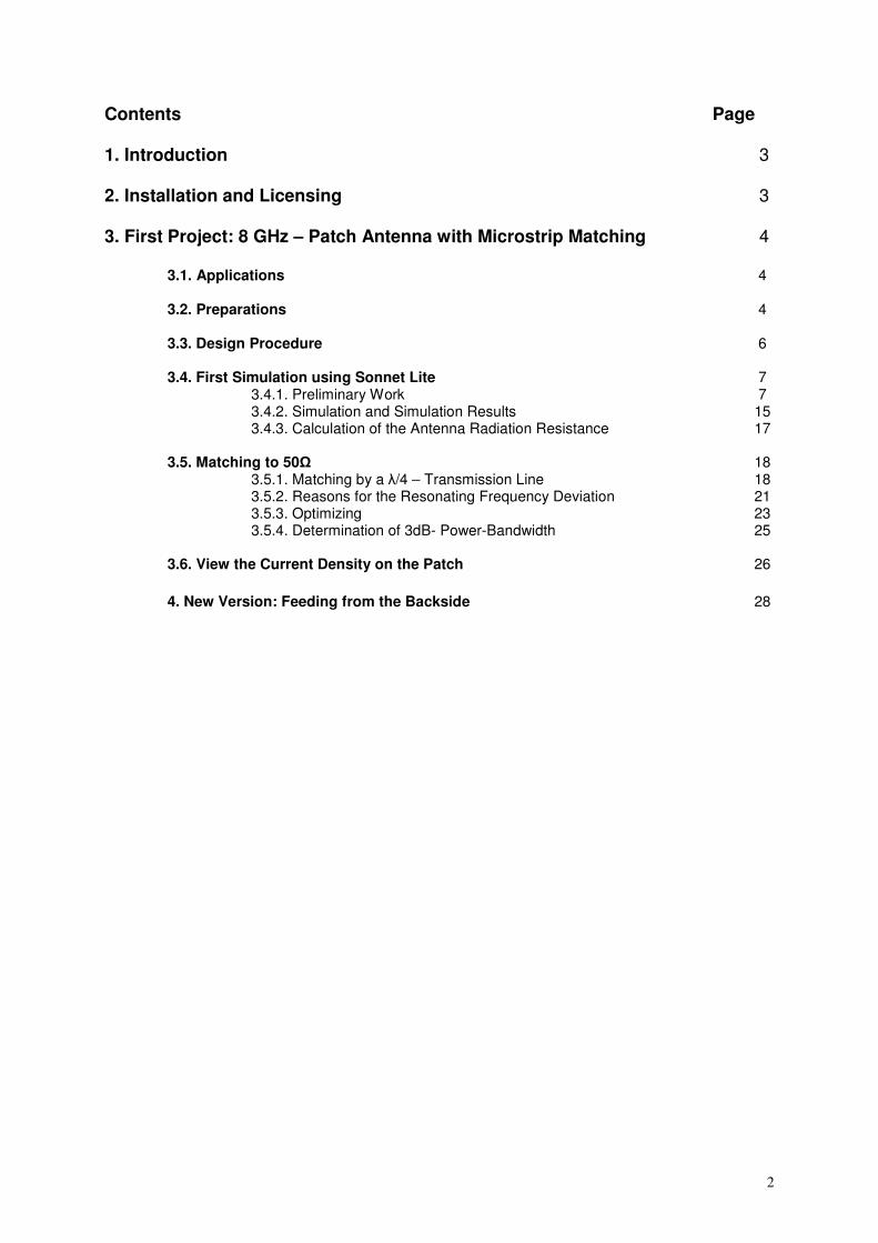
3. First Project: 5.8 GHz – Patch Antenna with Microstrip Matching 3.1. Applications When some years ago at Tettnang / Germany the new „Museum for Electronic History“ was opened there came very soon the demand for video monitoring to protect the exposed objects. But the museum at the second floor and the monitor at the entry of the historic building (including the restraint to drill holes through the walls for a cable connection) led to a wireless solution. So on the windowsill of the museum a 5.8GHz ISM module was installed which feeds a patch antenna with the camera signal. The radiated signal of the patch antenna is reflected by the wall of the neighbour’s house to the museum’s entry and to the ISM receiver including the monitor. A solution which works fine!
3.2. Preparations From the Internet we can get the following information concerning this ISM band: It consists of 16 channel with a spacing of 9 MHz. Channel 1 has a centre frequency of 5732 MHz, channel 16 uses 5867 MHz.
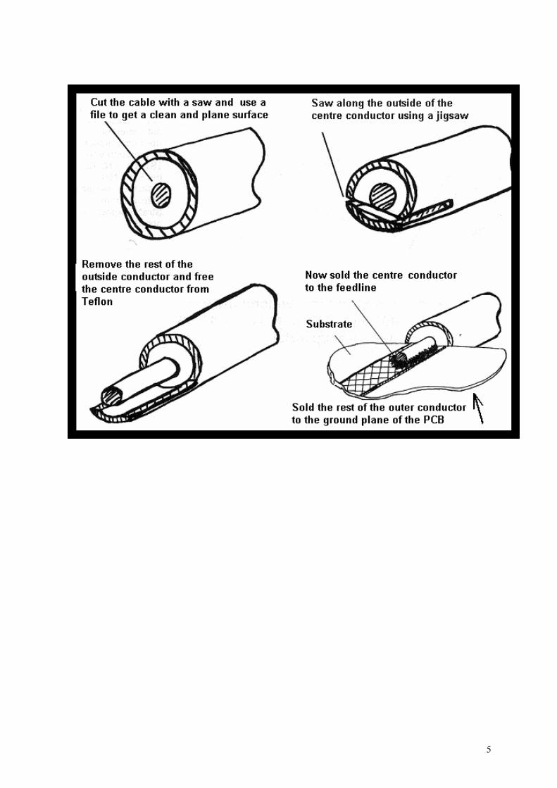
So the centre (=resonant) frequency of the antenna must be 5800 MHz and we need a bandwidth of 9 MHz x 16 = 144 MHz. Input Resistance at 5800 MHz must be 50 Ω. Properties of the used Rogers RO4003 PCB material: er = 3,38 Thickness = 32 MIL = 0,813mm Loss Tangent = 0.001 Copper cladding = 35 µm The outlines of the board are 50mm x 50mm. So we find at any point of the antenna a minimum distance between the antenna structure and the board’s edges of more than half a wavelength. Matching of the radiation resistance to 50Ω is realized by a microstrip λ/4 – line. To connect the end of the matching line and the centre conductor of the semi rigid cable (length = 10 cm) at the board’s edge we use a 50Ω microstrip line (= “feed line”). Very important is a correct connection between the semi rigid cable and the feed line to avoid reflections. The realization can be studied on the next side:
5
6
3.3. Design Procedure
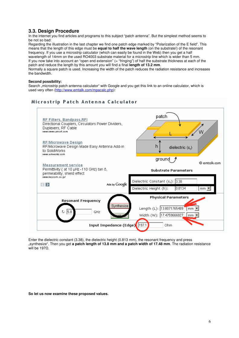
In the internet you find articles and programs to this subject “patch antenna”. But the simplest method seems to be not so bad: Regarding the illustration in the last chapter we find one patch edge marked by “Polarization of the E field”. This means that the length of this edge must be equal to half the wave length (on the substrate!) of the resonant frequency. If you use a microstrip calculator (which can easily be found in the Web) then you get a half wavelength of 14mm on the used RO4003 substrate material for a microstrip line which is wider than 5 mm. If you now take into account an “open end extension” (= “fringing”) of half the substrate thickness at each of the patch and reduce the length by this amount you will find a final length of 13.2 mm. Normally a square patch is used. Increasing the width of the patch reduces the radiation resistance and increases the bandwidth. Second possibility: Search „microstrip patch antenna calculator“ with Google and you get this link to an online calculator, which is used very often (http://www.emtalk.com/mpacalc.php):
Enter the dielectric constant (3.38), the dielectric height (0.813 mm), the resonant frequency and press „synthesize“. Then you get a patch length of 13.8 mm and a patch width of 17.48 mm. The radiation resistance will be 197Ω. So let us now examine these proposed values.
7
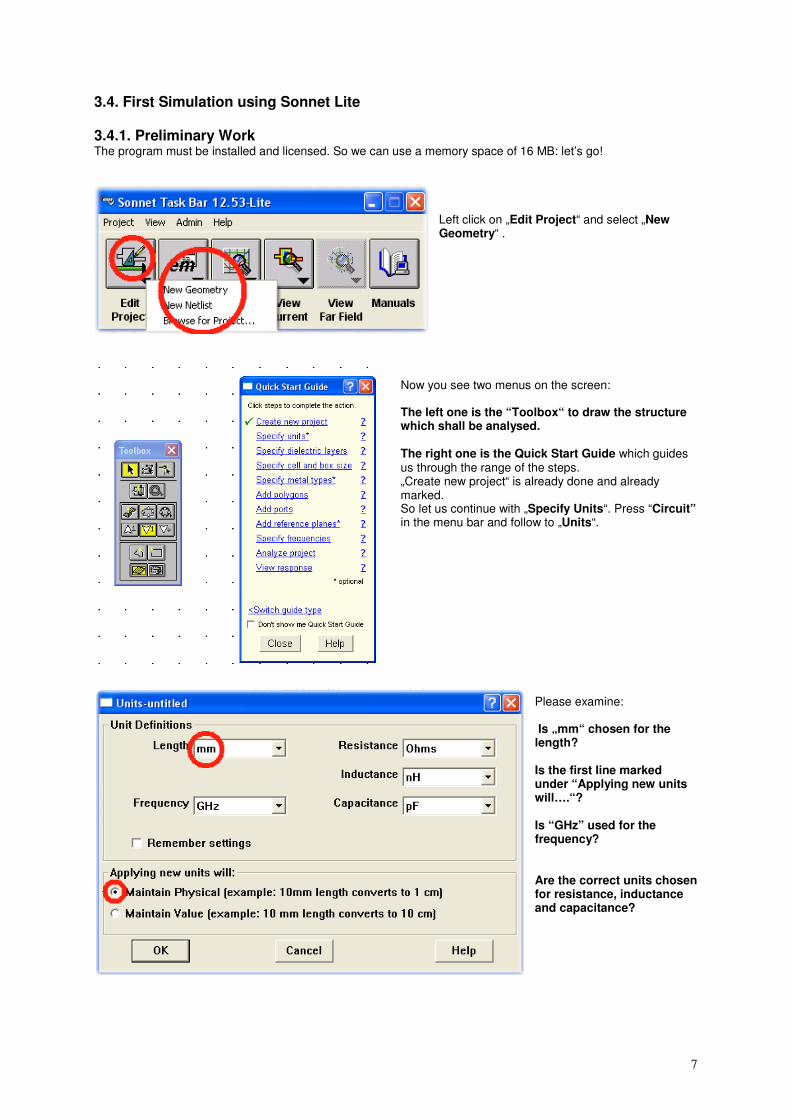
3.4. First Simulation using Sonnet Lite 3.4.1. Preliminary Work The program must be installed and licensed. So we can use a memory space of 16 MB: let’s go!
Left click on „Edit Project“ and select „New Geometry“ .
Now you see two menus on the screen: The left one is the “Toolbox“ to draw the structure which shall be analysed. The right one is the Quick Start Guide which guides us through the range of the steps. „Create new project“ is already done and already marked. So let us continue with „Specify Units“. Press “Circuit” in the menu bar and follow to „Units“.
Please examine: Is „mm“ chosen for the length? Is the first line marked under “Applying new units will….“? Is “GHz” used for the frequency? Are the correct units chosen for resistance, inductance and capacitance?
8
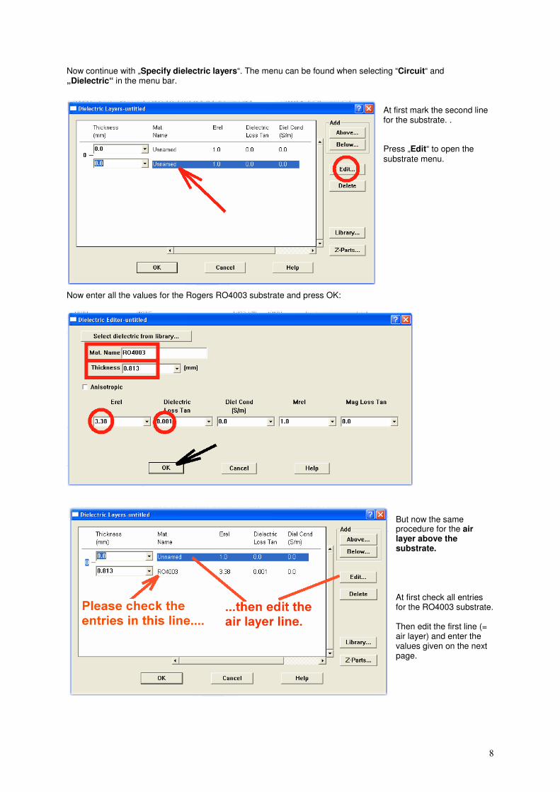
Now continue with „Specify dielectric layers“. The menu can be found when selecting “Circuit“ and „Dielectric“ in the menu bar.
At first mark the second line for the substrate. . Press „Edit“ to open the substrate menu.
Now enter all the values for the Rogers RO4003 substrate and press OK:
But now the same procedure for the air layer above the substrate. At first check all entries for the RO4003 substrate. Then edit the first line (= air layer) and enter the values given on the next page.
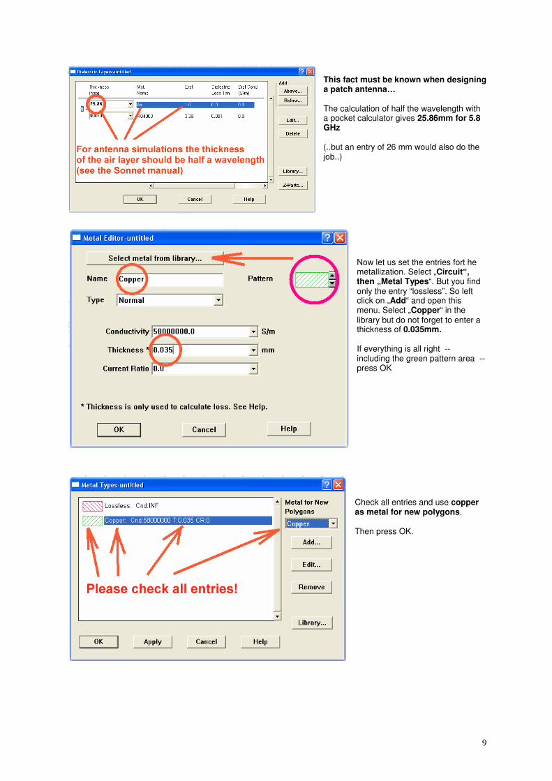
9
This fact must be known when designing a patch antenna… The calculation of half the wavelength with a pocket calculator gives 25.86mm for 5.8 GHz (..but an entry of 26 mm would also do the job..)
Now let us set the entries fort he metallization. Select „Circuit“, then „Metal Types“. But you find only the entry “lossless”. So left click on „Add“ and open this menu. Select „Copper“ in the library but do not forget to enter a thickness of 0.035mm. If everything is all right -- including the green pattern area -- press OK
Check all entries and use copper as metal for new polygons. Then press OK.
10
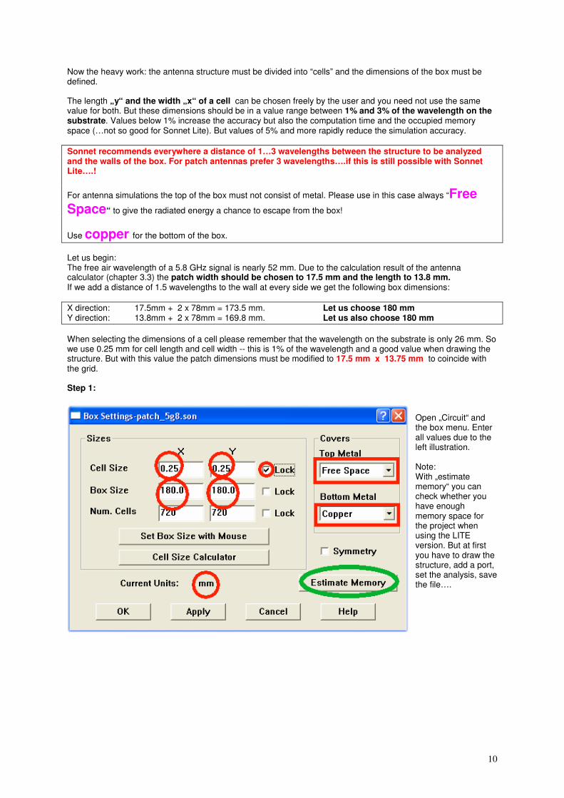
Now the heavy work: the antenna structure must be divided into “cells” and the dimensions of the box must be defined. The length „y“ and the width „x“ of a cell can be chosen freely by the user and you need not use the same value for both. But these dimensions should be in a value range between 1% and 3% of the wavelength on the substrate. Values below 1% increase the accuracy but also the computation time and the occupied memory space (…not so good for Sonnet Lite). But values of 5% and more rapidly reduce the simulation accuracy.
Sonnet recommends everywhere a distance of 1…3 wavelengths between the structure to be analyzed and the walls of the box. For patch antennas prefer 3 wavelengths….if this is still possible with Sonnet Lite….!
For antenna simulations the top of the box must not consist of metal. Please use in this case always “Free Space“ to give the radiated energy a chance to escape from the box!
Use copper for the bottom of the box.
Let us begin: The free air wavelength of a 5.8 GHz signal is nearly 52 mm. Due to the calculation result of the antenna calculator (chapter 3.3) the patch width should be chosen to 17.5 mm and the length to 13.8 mm. If we add a distance of 1.5 wavelengths to the wall at every side we get the following box dimensions:
X direction: 17.5mm + 2 x 78mm = 173.5 mm. Let us choose 180 mm Y direction: 13.8mm + 2 x 78mm = 169.8 mm. Let us also choose 180 mm
When selecting the dimensions of a cell please remember that the wavelength on the substrate is only 26 mm. So we use 0.25 mm for cell length and cell width -- this is 1% of the wavelength and a good value when drawing the structure. But with this value the patch dimensions must be modified to 17.5 mm x 13.75 mm to coincide with the grid. Step 1:
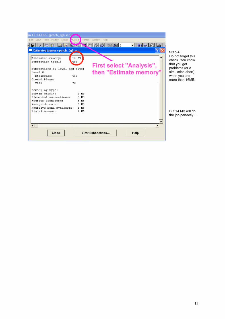
Open „Circuit“ and the box menu. Enter all values due to the left illustration. Note: With „estimate memory“ you can check whether you have enough memory space for the project when using the LITE version. But at first you have to draw the structure, add a port, set the analysis, save the file….
11
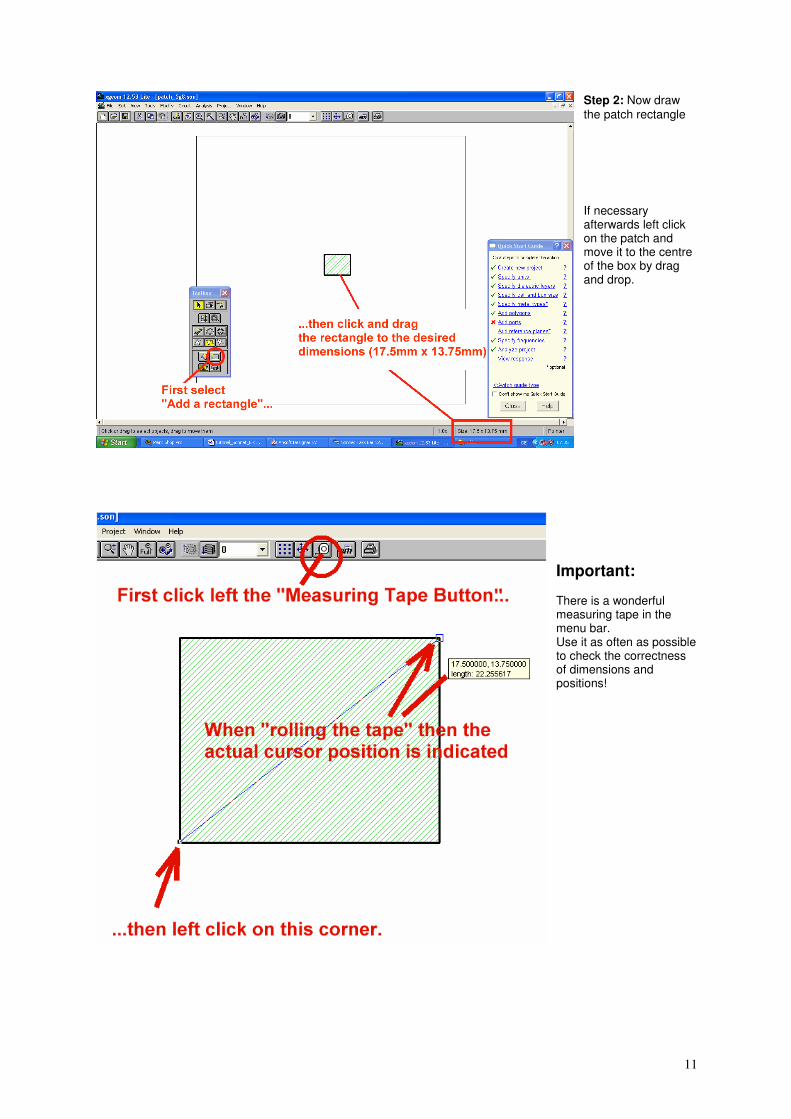
Step 2: Now draw the patch rectangle If necessary afterwards left click on the patch and move it to the centre of the box by drag and drop.
Important: There is a wonderful measuring tape in the menu bar. Use it as often as possible to check the correctness of dimensions and positions!
12
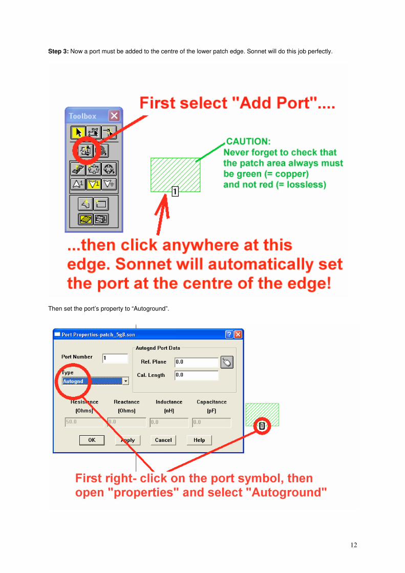
Step 3: Now a port must be added to the centre of the lower patch edge. Sonnet will do this job perfectly.
Then set the port’s property to “Autoground”.
13
Step 4: Do not forget this check. You know that you get problems (or a simulation abort) when you use more than 16MB. But 14 MB will do the job perfectly…
14
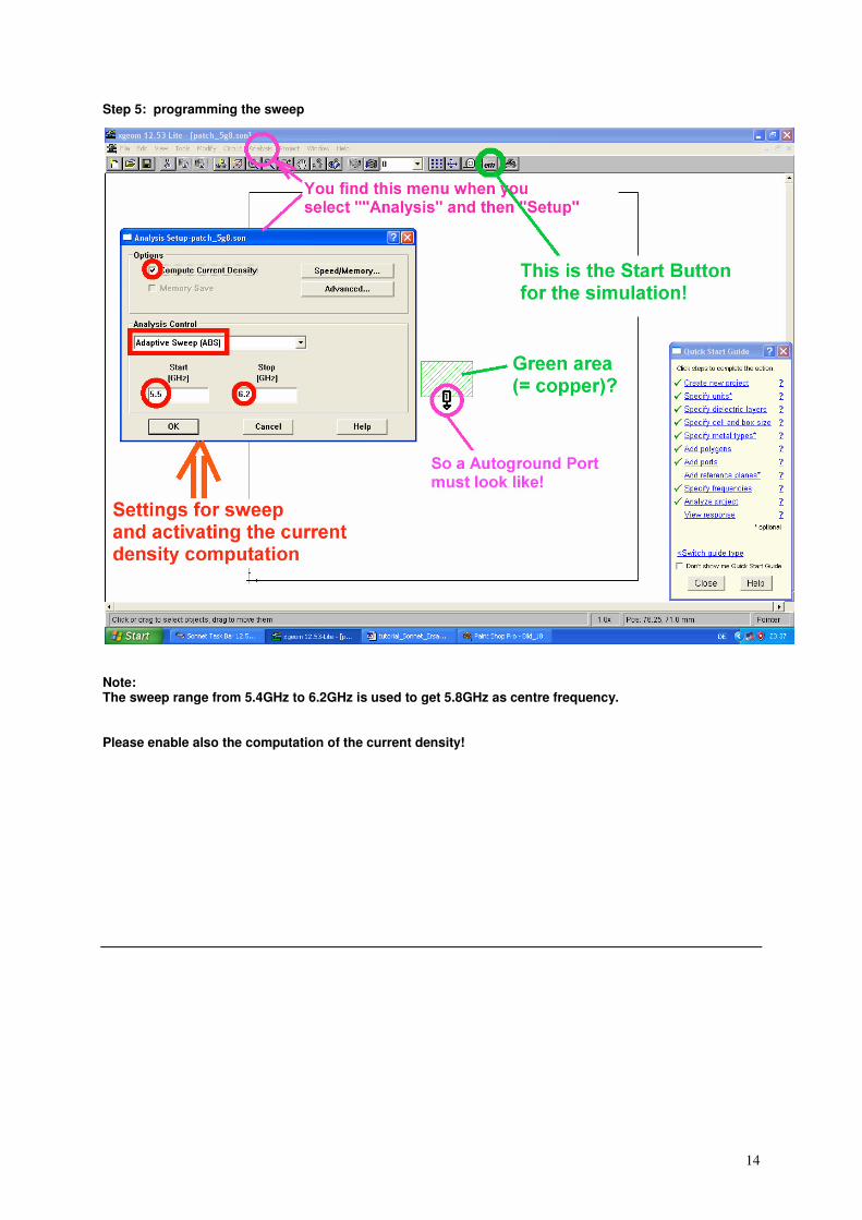
Step 5: programming the sweep
Note: The sweep range from 5.4GHz to 6.2GHz is used to get 5.8GHz as centre frequency. Please enable also the computation of the current density!
15
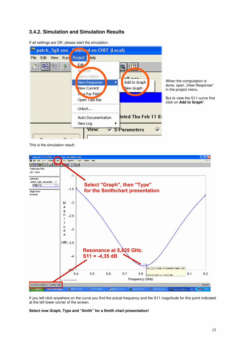
3.4.2. Simulation and Simulation Results If all settings are OK: please start the simulation.
When the computation is done, open „View Response“ in the project menu. But to view the S11-curve first click on Add to Graph“.
This is the simulation result:
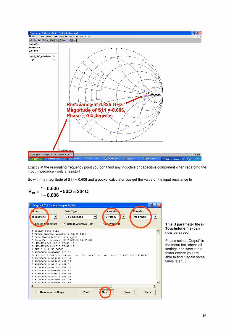
If you left click anywhere on the curve you find the actual frequency and the S11 magnitude for this point indicated at the left lower corner of the screen. Select now Graph, Type and “Smith” for a Smith chart presentation!
16
Exactly at the resonating frequency point you don’t find any inductive or capacitive component when regarding the input impedance - only a resistor! So with the magnitude of S11 = 0.606 and a pocket calculator you get the value of the input resistance to
204Ω50Ω0.6061
0.6061R IN =•
−
+=
This S parameter file (= Touchstone file) can now be saved. Please select „Output“ in the menu bar, check all settings and save it in a folder (where you are able to find it again some times later…).
17
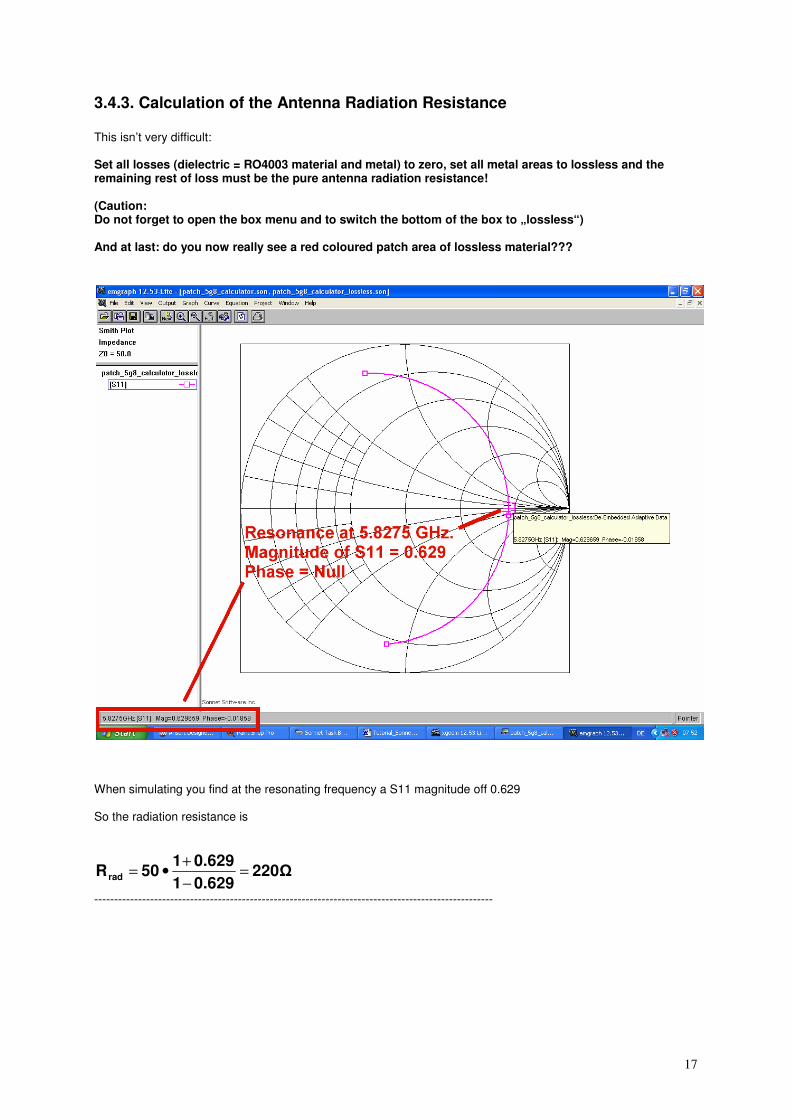
3.4.3. Calculation of the Antenna Radiation Resistance This isn’t very difficult: Set all losses (dielectric = RO4003 material and metal) to zero, set all metal areas to lossless and the remaining rest of loss must be the pure antenna radiation resistance! (Caution: Do not forget to open the box menu and to switch the bottom of the box to „lossless“) And at last: do you now really see a red coloured patch area of lossless material???
When simulating you find at the resonating frequency a S11 magnitude off 0.629 So the radiation resistance is
220Ω0.6291
0.629150R rad =
−
+•=
----------------------------------------------------------------------------------------------------
18
3.5. Matching to 50Ω
3.5.1. Matching by using a λ/4 transmission line
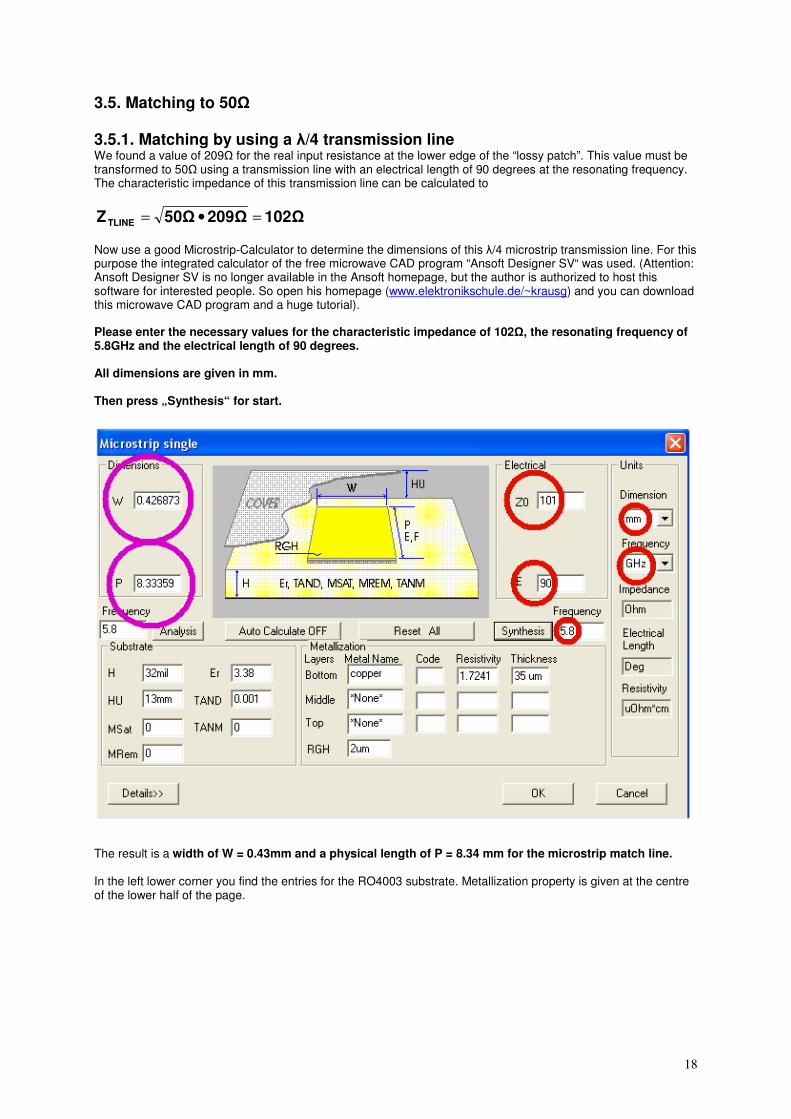
We found a value of 209Ω for the real input resistance at the lower edge of the “lossy patch”. This value must be transformed to 50Ω using a transmission line with an electrical length of 90 degrees at the resonating frequency. The characteristic impedance of this transmission line can be calculated to
102Ω209Ω50ΩZTLINE =•=
Now use a good Microstrip-Calculator to determine the dimensions of this λ/4 microstrip transmission line. For this purpose the integrated calculator of the free microwave CAD program “Ansoft Designer SV“ was used. (Attention: Ansoft Designer SV is no longer available in the Ansoft homepage, but the author is authorized to host this software for interested people. So open his homepage (www.elektronikschule.de/~krausg) and you can download this microwave CAD program and a huge tutorial). Please enter the necessary values for the characteristic impedance of 102Ω, the resonating frequency of 5.8GHz and the electrical length of 90 degrees. All dimensions are given in mm. Then press „Synthesis“ for start.
The result is a width of W = 0.43mm and a physical length of P = 8.34 mm for the microstrip match line. In the left lower corner you find the entries for the RO4003 substrate. Metallization property is given at the centre of the lower half of the page.
19
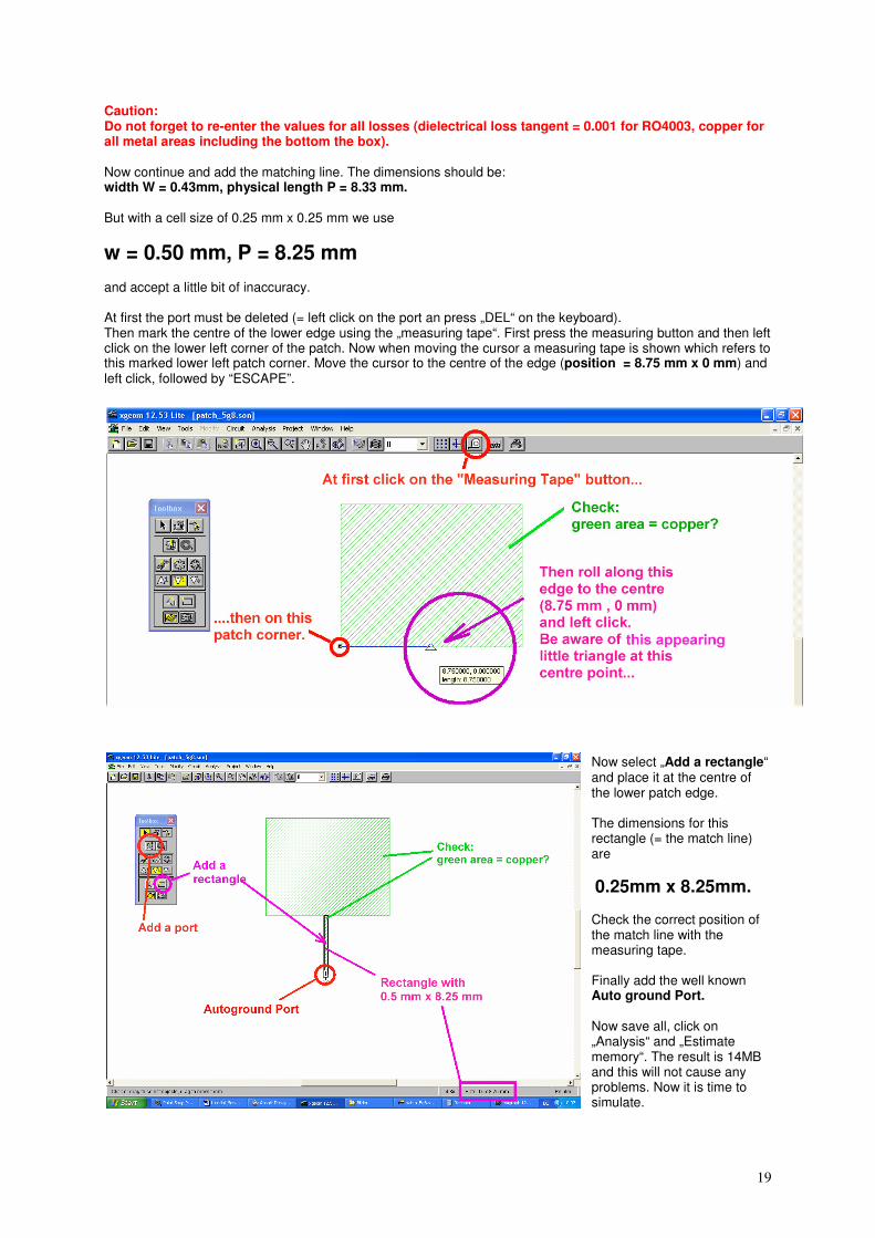
Caution: Do not forget to re-enter the values for all losses (dielectrical loss tangent = 0.001 for RO4003, copper for all metal areas including the bottom the box). Now continue and add the matching line. The dimensions should be: width W = 0.43mm, physical length P = 8.33 mm. But with a cell size of 0.25 mm x 0.25 mm we use
w = 0.50 mm, P = 8.25 mm
and accept a little bit of inaccuracy. At first the port must be deleted (= left click on the port an press „DEL“ on the keyboard). Then mark the centre of the lower edge using the „measuring tape“. First press the measuring button and then left click on the lower left corner of the patch. Now when moving the cursor a measuring tape is shown which refers to this marked lower left patch corner. Move the cursor to the centre of the edge (position = 8.75 mm x 0 mm) and left click, followed by “ESCAPE”.
Now select „Add a rectangle“ and place it at the centre of the lower patch edge. The dimensions for this rectangle (= the match line) are
0.25mm x 8.25mm. Check the correct position of the match line with the measuring tape. Finally add the well known Auto ground Port. Now save all, click on „Analysis“ and „Estimate memory“. The result is 14MB and this will not cause any problems. Now it is time to simulate.
20
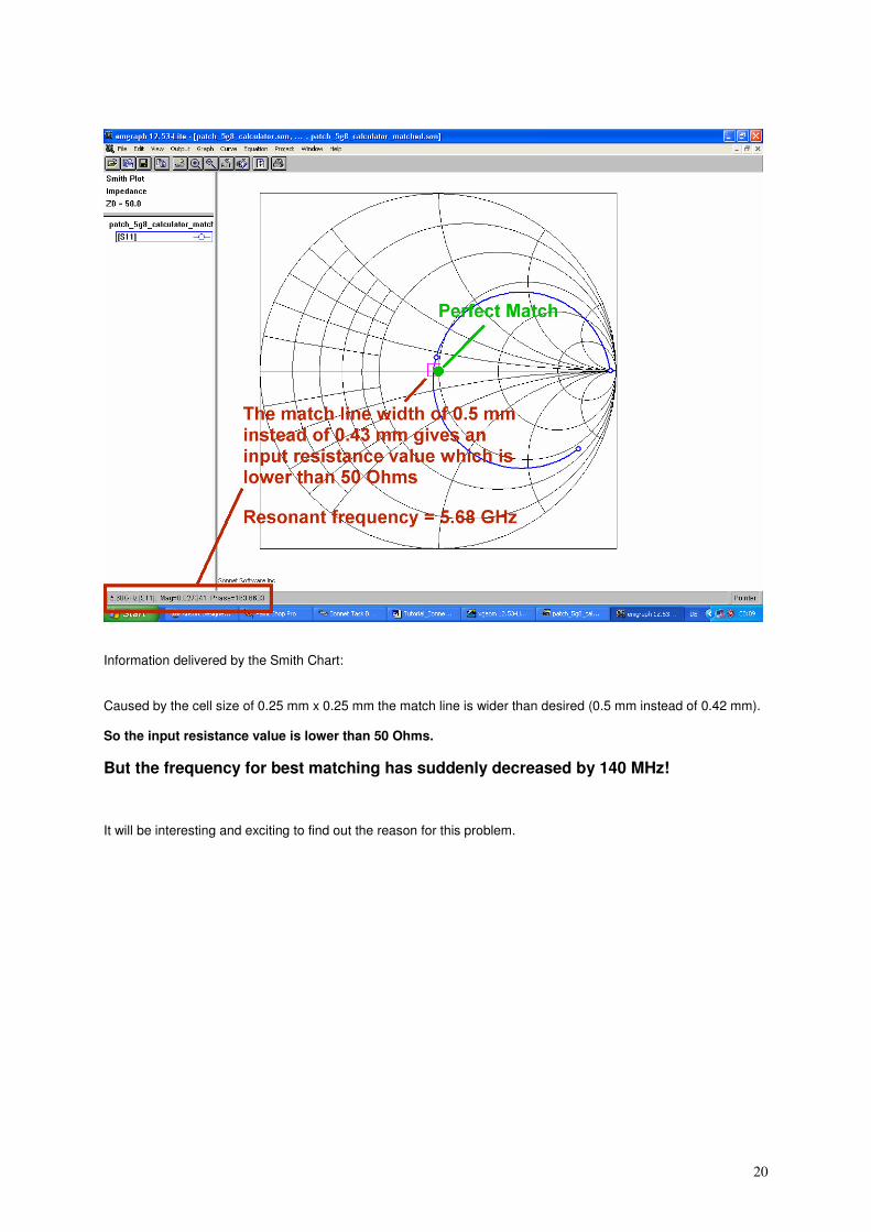
Information delivered by the Smith Chart: Caused by the cell size of 0.25 mm x 0.25 mm the match line is wider than desired (0.5 mm instead of 0.42 mm). So the input resistance value is lower than 50 Ohms.
But the frequency for best matching has suddenly decreased by 140 MHz! It will be interesting and exciting to find out the reason for this problem.
21
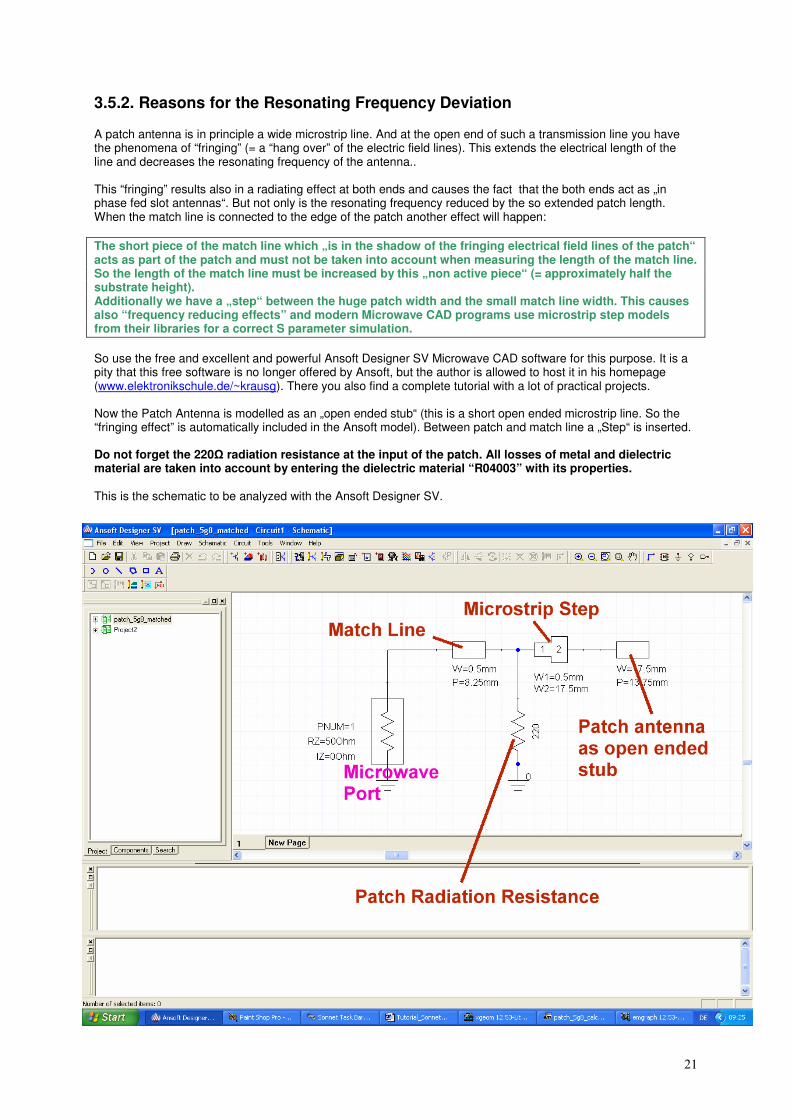
3.5.2. Reasons for the Resonating Frequency Deviation A patch antenna is in principle a wide microstrip line. And at the open end of such a transmission line you have the phenomena of “fringing” (= a “hang over” of the electric field lines). This extends the electrical length of the line and decreases the resonating frequency of the antenna.. This “fringing” results also in a radiating effect at both ends and causes the fact that the both ends act as „in phase fed slot antennas“. But not only is the resonating frequency reduced by the so extended patch length. When the match line is connected to the edge of the patch another effect will happen:
The short piece of the match line which „is in the shadow of the fringing electrical field lines of the patch“ acts as part of the patch and must not be taken into account when measuring the length of the match line. So the length of the match line must be increased by this „non active piece“ (= approximately half the substrate height). Additionally we have a „step“ between the huge patch width and the small match line width. This causes also “frequency reducing effects” and modern Microwave CAD programs use microstrip step models from their libraries for a correct S parameter simulation.
So use the free and excellent and powerful Ansoft Designer SV Microwave CAD software for this purpose. It is a pity that this free software is no longer offered by Ansoft, but the author is allowed to host it in his homepage (www.elektronikschule.de/~krausg). There you also find a complete tutorial with a lot of practical projects. Now the Patch Antenna is modelled as an „open ended stub“ (this is a short open ended microstrip line. So the “fringing effect” is automatically included in the Ansoft model). Between patch and match line a „Step“ is inserted. Do not forget the 220Ω radiation resistance at the input of the patch. All losses of metal and dielectric material are taken into account by entering the dielectric material “R04003” with its properties. This is the schematic to be analyzed with the Ansoft Designer SV.
22
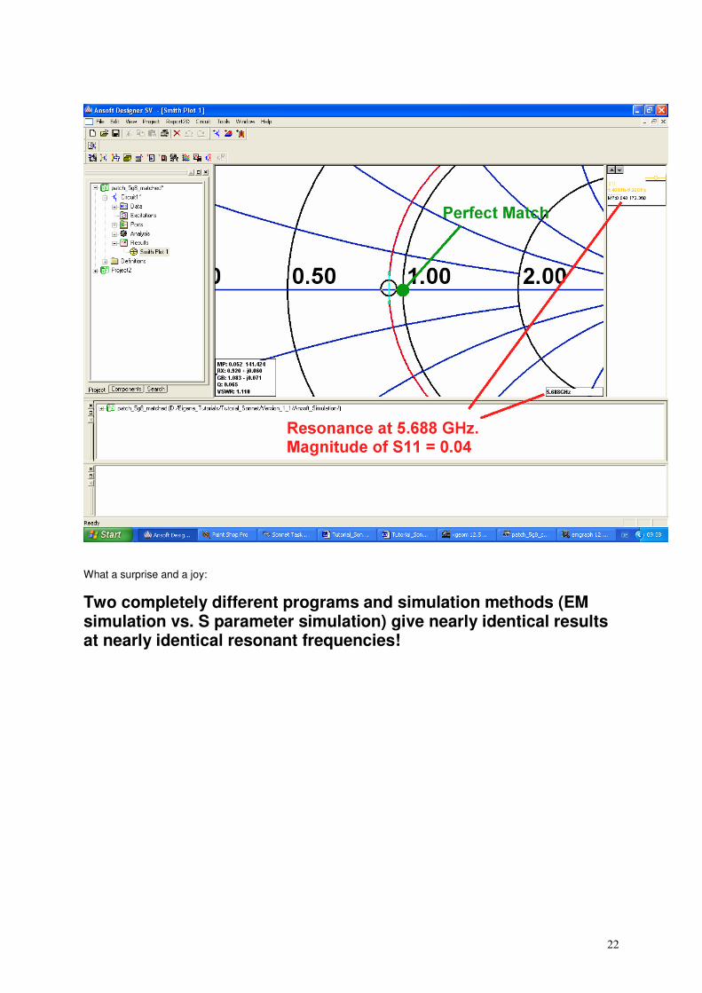
What a surprise and a joy:
Two completely different programs and simulation methods (EM simulation vs. S parameter simulation) give nearly identical results at nearly identical resonant frequencies!
23
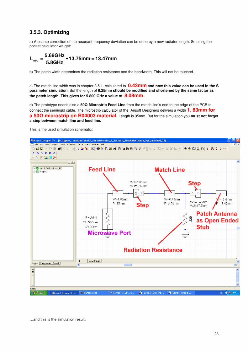
3.5.3. Optimizing a) A coarse correction of the resonant frequency deviation can be done by a new radiator length. So using the pocket calculator we get:
13.47mm13.75mm5.8GHz
5.68GHzLneu =•=
b) The patch width determines the radiation resistance and the bandwidth. This will not be touched.
c) The match line width was in chapter 3.5.1. calculated to 0.43mm and now this value can be used in the S
parameter simulation. But the length of 8.25mm should be modified and shortened by the same factor as
the patch length. This gives for 5.800 GHz a value of 8.08mm.
d) The prototype needs also a 50Ω Microstrip Feed Line from the match line’s end to the edge of the PCB to
connect the semirigid cable. The microstrip calculator of the Ansoft Designers delivers a width 1. 83mm for a 50Ω microstrip on R04003 material. Length is 35mm. But for the simulation you must not forget
a step between match line and feed line. This is the used simulation schematic:
…and this is the simulation result:
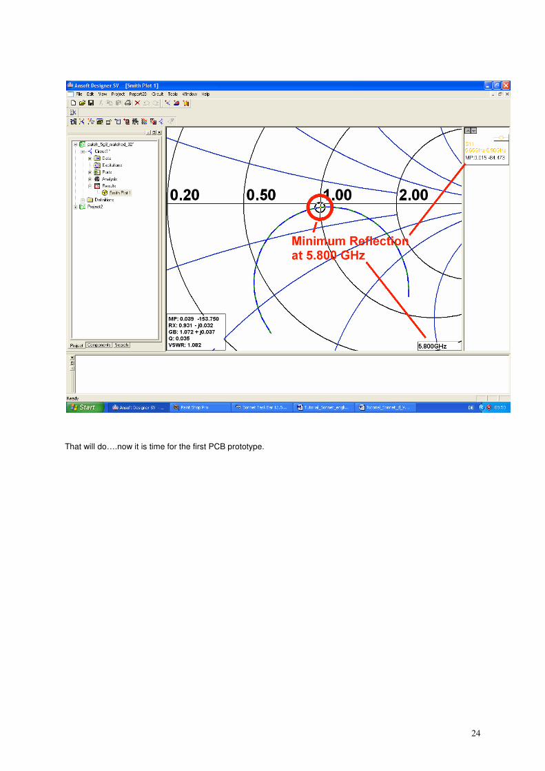
24
That will do….now it is time for the first PCB prototype.
25
3.5.4. Determination of the Power Bandwidth This is more difficult because now we must think in „powers“. The unit for the incident and the reflected wave is „Volt“ but you should remember: In reality powers are travelling on a transmission line -- the incident wave from the generator to the load at the end of a cable and the reflected wave back from the load to the generator. So the unit “Volt” comes from applying a square root to the powers when regarding these waves -- to avoid “Watts” and to measure “Volts” in practice and in a circuit. If you now are looking for the frequency values at which the radiated power is reduced by 30% due to reflection you need to calculate as follows. In this case 30% of the incident power are reflected and travel back to the generator:
2
2
incident
reflected
incident
reflected r0.3U
U
P
P==
=
Now you get „r“ (which is the magnitude of S11) to
0.550.3r ==
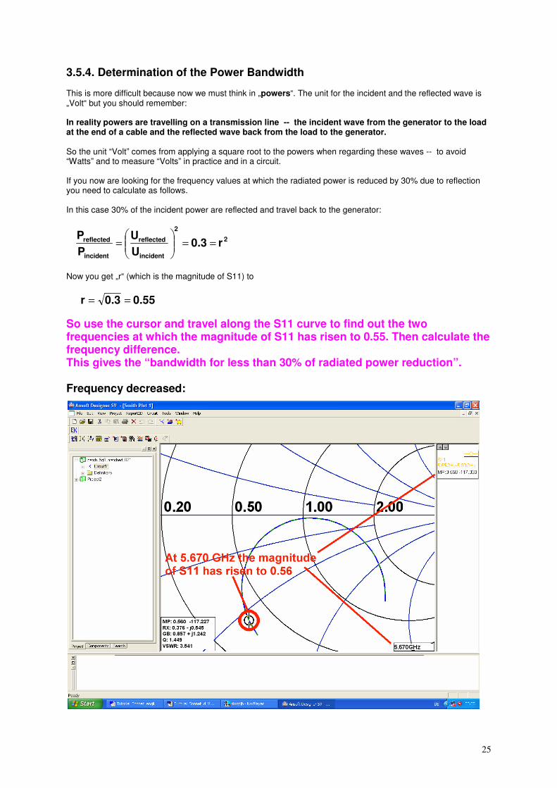
So use the cursor and travel along the S11 curve to find out the two frequencies at which the magnitude of S11 has risen to 0.55. Then calculate the frequency difference. This gives the “bandwidth for less than 30% of radiated power reduction”. Frequency decreased:
26
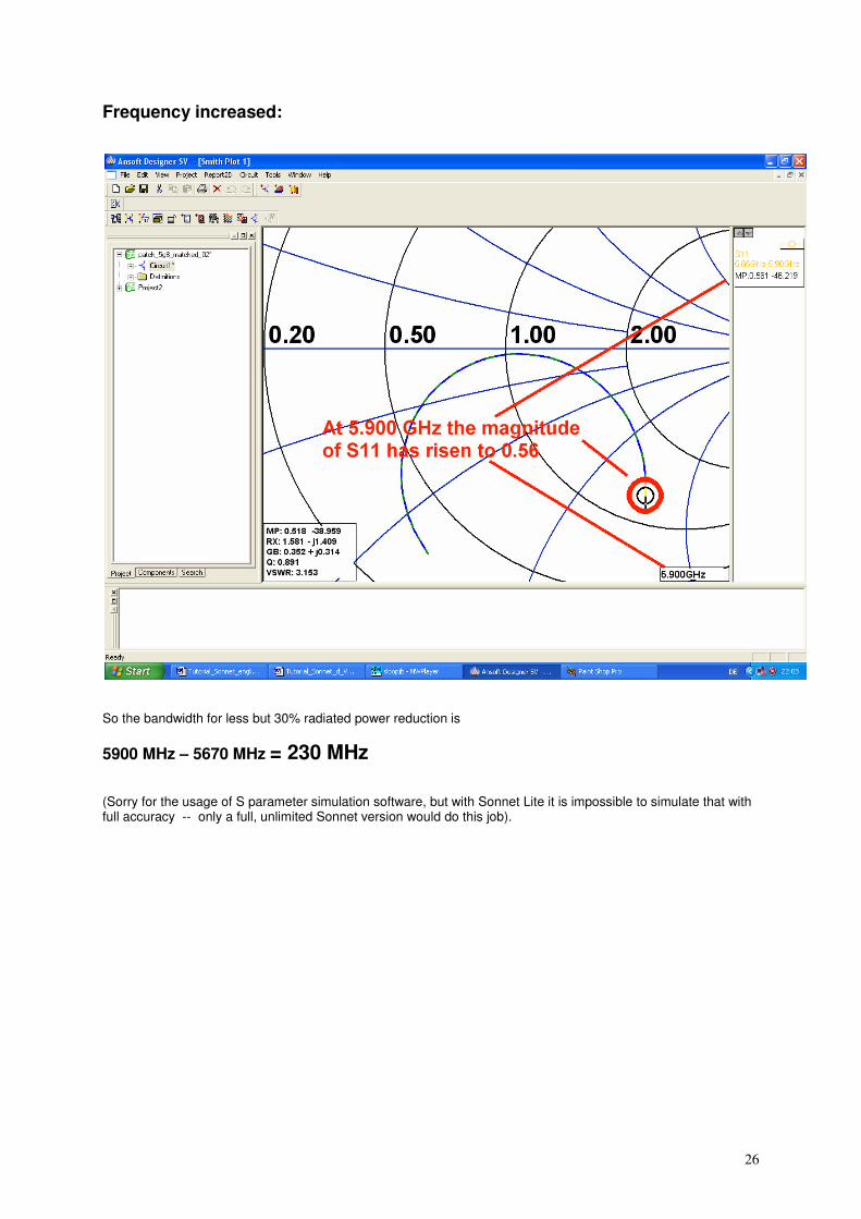
Frequency increased:
So the bandwidth for less but 30% radiated power reduction is
5900 MHz – 5670 MHz = 230 MHz (Sorry for the usage of S parameter simulation software, but with Sonnet Lite it is impossible to simulate that with full accuracy -- only a full, unlimited Sonnet version would do this job).
27
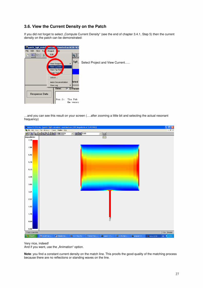
3.6. View the Current Density on the Patch If you did not forget to select „Compute Current Density“ (see the end of chapter 3.4.1, Step 5) then the current density on the patch can be demonstrated:
Select Project and View Current…..
…and you can see this result on your screen (….after zooming a little bit and selecting the actual resonant frequency)
Very nice, indeed! And if you want, use the „Animation“ option. Note: you find a constant current density on the match line. This proofs the good quality of the matching process because there are no reflections or standing waves on the line.
28
4. Another possibility: Feeding from the Backside: Using a match line and a feed line increases the dimensions of the PCB for the antenna. So another way was tested out. On the patch we find a voltage distribution with a sine wave form. At every radiating edge we find a voltage maximum but at the centre the voltage crosses Zero.
At the radiating edge a radiation resistance of 220Ω can be measured but when moving in direction to the centre the resistance decreases to Zero (due to a voltage amplitude of Zero at this point). So on this way we pass an input resistance of 50Ω and we can now at this point feed the antenna by a SMA connector which is soldered on the backside and it’s centre conductor passes through the R04003 material. To find out this point we regard the first patch design of chapter 3.4.1. The patch dimensions were
17.5mm x 13.75 mm and at the patch edge an input resistance of ca. 200Ω (exactly: 204Ω) can be
measured. The voltage at the edge equates to the maximum value of a sine function at an angle of 90 degrees:
max0
maxEdge U)sin(90UU =•=
We need an input resistance of 50Ω which equates to a quarter of 200Ω. But power changes with the square of the voltage and so we get at the 50Ω point half the voltage amplitude for the same input power. Due to the sine variation of the voltage along the patch this means that we find an angle of 30 degrees for a sine value of 0.5 -- and 30 degrees are 90 degrees divided by 3. So it is now easy to find the feed point, because 90 degrees equate half the patch length of 13.75mm:
2.3mm2
13.75mm
3
1x =
•
=
This is measured from the centre in direction to the patch edge. Otherwise when starting at the radiating patch edge we find the point for the necessary “Via” (to solder the centre conductor of the SMA socket to the patch) at
4.575mm2.3mm2
13.75mmY =−=
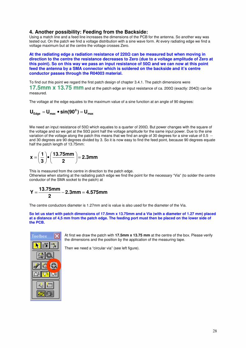
The centre conductors diameter is 1.27mm and is value is also used for the diameter of the Via. So let us start with patch dimensions of 17.5mm x 13.75mm and a Via (with a diameter of 1.27 mm) placed at a distance of 4,5 mm from the patch edge. The feeding port must then be placed on the lower side of the PCB.
At first we draw the patch with 17.5mm x 13.75 mm at the centre of the box. Please verify the dimensions and the position by the application of the measuring tape. Then we need a “circular via” (see left figure).
29
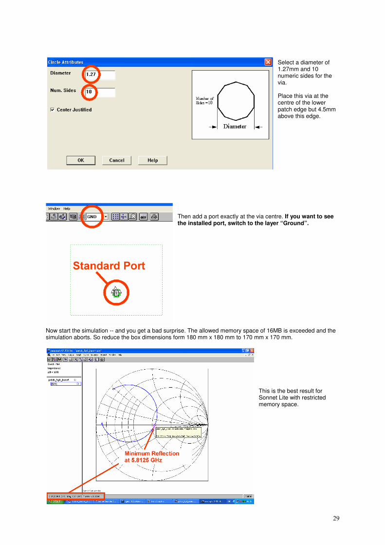
Select a diameter of 1.27mm and 10 numeric sides for the via. Place this via at the centre of the lower patch edge but 4.5mm above this edge.
Then add a port exactly at the via centre. If you want to see the installed port, switch to the layer “Ground”.
Now start the simulation -- and you get a bad surprise. The allowed memory space of 16MB is exceeded and the simulation aborts. So reduce the box dimensions form 180 mm x 180 mm to 170 mm x 170 mm.
This is the best result for Sonnet Lite with restricted memory space.
30
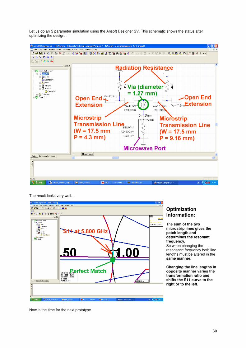
Let us do an S parameter simulation using the Ansoft Designer SV. This schematic shows the status after optimizing the design.
The result looks very well…
Optimization information: The sum of the two microstrip lines gives the patch length and determines the resonant frequency. So when changing the resonance frequency both line lengths must be altered in the same manner. Changing the line lengths in opposite manner varies the transformation ratio and shifts the S11 curve to the right or to the left.
Now is the time for the next prototype.