Embed Size (px)
Citation preview

EM9209
Copyright 2017, EM Microelectronic-Marin SA 9209-DS, Version 4.3 , 21-Dec-17
1 www.emmicroelectronic.com
EM9209: High Sensitivity, 1.5-72kbps, 2.4GHz FSK Transceiver
Description
The EM9209 is a 1.5kbps to 72kbps low-power, low-voltage, single chip 2.4GHz ISM band RF transceiver ideal for battery operated wireless applications such as wireless sensors and control, gaming, human interface devices, and security networks.
The EM9209's built-in custom low power micro-controller supports the proprietary wireless protocol links in the license-free 2.4000GHz to 2.4835GHz ISM band. It includes a low-IF receiver architecture and uses FSK modulation. A SPI interface provides a simple control of the baseband using an external host controller.
The EM9209 provides two communication modes with normal or high sensitivity and programmable bit rate from 1.5kbps to 72kbps.
The EM9209 provides a divided clock output programmable at either 32.5kHz, 325kHz or 3.25MHz to drive external micro-controllers time reference.
Simplified Application Schematic
EM9209
VB
AT
AN
TN
AN
TP
DIV
_C
K
Host Controller
VS
S_IS
OX
OU
TX
IN
EN
_R
EG
TX
_O
N
RX
_O
N
SC
K
SS MO
SI
MIS
O
VS
S_D
IG
IRQ
VS
S_
RX
TX
VD
D_
RX
TX
VS
S_
RX
TX
VS
S_D
IGV
DD
_
SY
NT
H
VS
S_
SY
NT
HV
PR
OG
Features
Low Voltage:
1.9V to 3.6V battery operation
Low Power:
7mA in RX normal sensitivity mode (NS)
8mA in RX high sensitivity mode (HS)
TX Mode: 11mA @-1dBm, 36mA @+10dBm
<150A in Stand-by Mode
<10nA in Power Down Mode
High Performance:
-115dBm sensitivity at 1.5kbps
+10dBm maximum received input signal
Programmable output power from -20dBm to +10dBm
Ultra compact radio design with low BOM cost:
COB with 4mm x 4mm footprint
Operating Temperature: -40°C to +85°C
Direct antenna interface (200 Ω differential)
Low-cost 26MHz crystal oscillator, frequency tolerance over temperature and aging of ±20ppm, with adjusted initial value
Flexible interface:
SPI interface for microcontrollers
Fully programmable link layer
External PA and LNA control signal available on 2 pads
Available as die or in MLF24 4x4mm package
Typical Applications
Remote sensing and control
Wireless mice, keyboards, toys etc…
Wireless watch sensors, sports equipment
Alarm and security systems MLF24 Pinout
EM MICROELECTRONIC - MARIN SA

EM9209
Copyright 2017, EM Microelectronic-Marin SA 9209-DS, Version 4.3 , 21-Dec-17
2 www.emmicroelectronic.com
Table of Contents 1. Introduction ....................................................................................................................................................................... 6
1.1 Overview .......................................................................................................................................................................... 6 1.2 Applications schematic and block diagram ....................................................................................................................... 6 1.3 RF transceiver .................................................................................................................................................................. 7
1.3.1 Frequency synthesizer / Phase-Locked Loop (PLL) ............................................................................................... 7 1.3.2 Receiver .................................................................................................................................................................. 7 1.3.3 Transmitter .............................................................................................................................................................. 7
1.4 Digital interface ................................................................................................................................................................. 7 1.4.1 Baseband micro-controller ...................................................................................................................................... 8
1.4.1.1 In Communication mode: ............................................................................................................................... 8 1.4.1.2 In Auto-calibration mode: ............................................................................................................................... 8 1.4.1.3 In Standby mode: .......................................................................................................................................... 8 1.4.1.4 In RAM2 initialization mode ............................................................................................................................ 8
1.5 Power management ......................................................................................................................................................... 8 1.5.1 RF transceiver supply ............................................................................................................................................. 8 1.5.2 Digital supply ........................................................................................................................................................... 9 1.5.3 Bias generator ......................................................................................................................................................... 9
2. Pin information................................................................................................................................................................ 10 3. Electrical specifications .................................................................................................................................................. 11
3.1 Handling procedures and absolute maximum ratings ..................................................................................................... 11 3.2 General operating conditions .......................................................................................................................................... 11 3.3 Electrical characteristics ................................................................................................................................................. 11 3.4 Timing characteristics ..................................................................................................................................................... 13
4. Functional modes ........................................................................................................................................................... 14 4.1 Operational modes ......................................................................................................................................................... 14
4.1.1 Power down .......................................................................................................................................................... 14 4.1.2 Standby mode ....................................................................................................................................................... 14 4.1.3 RAM2 Init mode ...................................................................................................................................................... 14 4.1.4 Auto-calibration modes ......................................................................................................................................... 14 4.1.5 Transmit (TX) mode .............................................................................................................................................. 15 4.1.6 Receive (RX) mode ............................................................................................................................................... 15
5. User interface ................................................................................................................................................................. 16 5.1 Digital interface ............................................................................................................................................................... 16
5.1.1 SPI operations ...................................................................................................................................................... 16 5.1.1.1 Status bits: Status[2:0] .......................................................................................................................... 17 5.1.1.2 SPI command: Read_RXFIFO .................................................................................................................... 17 5.1.1.3 SPI command: Write_TXFIFO .................................................................................................................. 18 5.1.1.4 SPI command: Read_RXFIFO_Size .......................................................................................................... 18 5.1.1.5 SPI command: Read_TXFIFO_Size .......................................................................................................... 18 5.1.1.6 SPI command: Read_RAM1 ......................................................................................................................... 19 5.1.1.7 SPI command: Write_RAM1 ...................................................................................................................... 19 5.1.1.8 SPI command: Read_RAM2 ......................................................................................................................... 19 5.1.1.9 SPI command: Write_RAM2 .................................................................................................................... 19 5.1.1.10 SPI command: Reset_Micro .................................................................................................................... 19 5.1.1.11 SPI command: Stop_Micro ...................................................................................................................... 19 5.1.1.12 SPI command: Start_Micro .................................................................................................................... 19 5.1.1.13 SPI command: Clear_IRQ ......................................................................................................................... 19 5.1.1.14 SPI command: Send_TXFIFO .................................................................................................................... 20 5.1.1.15 SPI command: Aux_com ............................................................................................................................. 20 5.1.1.16 SPI command: ROM_Boot ........................................................................................................................... 20 5.1.1.17 SPI command: ROM_Boot0_and_Start ................................................................................................... 20
5.2 Programming interface ................................................................................................................................................... 21 5.2.1 RAM2, RAM1 reset ............................................................................................................................................... 21 5.2.2 RAM2 Initialization ................................................................................................................................................ 21 5.2.3 Internal PTAT current auto-calibration .................................................................................................................. 21 5.2.4 VCO code auto-calibration .................................................................................................................................... 22 5.2.5 External Clock frequency (on DIV_CK terminal) ................................................................................................... 22 5.2.6 Channel Data rate ................................................................................................................................................. 23 5.2.7 RF Frequency of operation ................................................................................................................................... 24 5.2.8 Address Byte ......................................................................................................................................................... 24 5.2.9 Bit stuffing ............................................................................................................................................................. 25 5.2.10 TX power level ...................................................................................................................................................... 25 5.2.11 External PA and LNA control ................................................................................................................................ 25 5.2.12 Packet (TX and RX) payload................................................................................................................................. 25
5.2.12.18 Mode payload size in the header: ........................................................................................................... 25 5.2.12.19 Mode payload size in RAM2: ................................................................................................................... 26

EM9209
Copyright 2017, EM Microelectronic-Marin SA 9209-DS, Version 4.3 , 21-Dec-17
3 www.emmicroelectronic.com
5.2.13 Registers: TXFIFO and RXFIFO ........................................................................................................................... 26 5.2.14 Transmission flow, “high sensitivity”, mode payload defined in RAM2, quick control (automatic ROMboot). ......... 26 5.2.15 Reception flow, “high sensitivity”, mode payload defined in RAM2, quick control (automatic ROMboot). .............. 26 5.2.16 Transmission flow, “high sensitivity”, mode entire TXFIFO, manual control (step by step). .................................. 27 5.2.17 Reception flow, “high sensitivity”, mode payload size in header, manual control (step by step). .......................... 28 5.2.18 Transmission flow, “high sensitivity”, mode payload size defined in RAM2 ............................................................ 29 5.2.19 Reception flow, “high sensitivity”, mode payload size defined in RAM2 ................................................................. 29 5.2.20 Transmission flow, “normal sensitivity”, mode entire TXFIFO ............................................................................... 29 5.2.21 Reception flow, “normal sensitivity”, mode payload size in header ....................................................................... 29 5.2.22 Transmission flow, “normal sensitivity”, mode payload size defined in RAM2 ........................................................ 29 5.2.23 Reception flow, “normal sensitivity”, mode payload size defined in RAM2 ............................................................. 30 5.2.24 Received Signal Strength Indicator (RSSI) ........................................................................................................... 30 5.2.25 Transparent mode ................................................................................................................................................. 30 5.2.26 Frequency Error Register: DFT_Mes[7:0] .......................................................................................................... 30 5.2.27 Microcontroller ROMboot Instruction Disable: RB_Inst_Dis .............................................................................. 30
5.3 Description of RAM2 and registers mapping .................................................................................................................... 31 5.3.1 Memory RAM2[11:0] @ address 0 ..................................................................................................................... 31 5.3.2 Memory RAM2[11:0] @ address 1 ..................................................................................................................... 31 5.3.3 Memory RAM2[11:0] @ address 2 ..................................................................................................................... 32 5.3.4 Memory RAM2[11:0] @ address 3 ..................................................................................................................... 32 5.3.5 Memory RAM2[11:0] @ address 4 ..................................................................................................................... 33 5.3.6 Memory RAM2[11:0] @ address 5 ..................................................................................................................... 33 5.3.7 Memory RAM2[11:0] @ address 6 ..................................................................................................................... 34 5.3.8 Memory RAM2[11:0] @ address 7 ..................................................................................................................... 34 5.3.9 Memory RAM2[11:0] @ address 8 ..................................................................................................................... 35 5.3.10 Memory RAM2[11:0] @ address 9 ..................................................................................................................... 35 5.3.11 Memory RAM2[11:0] @ address 10 ................................................................................................................... 36 5.3.12 Memory RAM2[11:0] @ address 11 ................................................................................................................... 36 5.3.13 Memory RAM2[11:0] @ address 12 ................................................................................................................... 37 5.3.14 Memory RAM2[11:0] @ address 13 ................................................................................................................... 37 5.3.15 Memory RAM2[11:0] @ address 14 ................................................................................................................... 38 5.3.16 Memory RAM2[11:0] @ address 15 ................................................................................................................... 38
6. Packet information .......................................................................................................................................................... 39 6.1 Packet format ................................................................................................................................................................. 39
7. Versions and ordering information .................................................................................................................................. 40 8. Die Pinout ....................................................................................................................................................................... 40 9. Package information ....................................................................................................................................................... 41
9.1 Package marking ............................................................................................................................................................ 41 10. Typical Applications ........................................................................................................................................................ 42
10.1 Application schematics .............................................................................................................................................. 42

EM9209
Copyright 2017, EM Microelectronic-Marin SA 9209-DS, Version 4.3 , 21-Dec-17
4 www.emmicroelectronic.com
Table of Figures Figure 1: Simplified block diagram, die pin-out ............................................................................................................................... 6 Figure 2: Digital Interface topology ................................................................................................................................................. 8 Figure 3: Example of state diagram of EM9209 modes ................................................................................................................ 14 Figure 4: SPI timing diagram ........................................................................................................................................................ 16 Figure 5 : timing of the SPI Read_RXFIFO / Write_TXFIFO command .................................................................................... 18 Figure 5 : On-air data rate selection ............................................................................................................................................. 23 Figure 6: U9209 Die Pinout........................................................................................................................................................... 40 Figure 7: Example application schematic of the EM9209 ............................................................................................................. 42
Table of Tables Table 1: EM9209 pinout (die version only) ................................................................................................................................... 10 Table 2: Absolute maximum ratings .............................................................................................................................................. 11 Table 3: General operating conditions .......................................................................................................................................... 11 Table 4: Supply currents on VBAT ................................................................................................................................................ 11 Table 5: DC characteristics ........................................................................................................................................................... 12 Table 6: RF characteristics ........................................................................................................................................................... 12 Table 9: SPI timing values. ........................................................................................................................................................... 17 Table 10: Ck_Pad Frequencies .................................................................................................................................................... 22 Table 11: Channel Data Rate ....................................................................................................................................................... 23 Table 12: Channel Frequency Selection ....................................................................................................................................... 24 Table 13: “On air” versus Minimum Bit stuffed Data Rates ........................................................................................................... 25 Table 15: Packet format, normal sensitivity mode ........................................................................................................................ 39 Table 16: Packet format, high sensitivity mode............................................................................................................................. 39 Table 17: Version information ....................................................................................................................................................... 40 Table 18: Ordering information ..................................................................................................................................................... 40 Table 19: EM9209 application schematic external component details .......................................................................................... 43

EM9209
Copyright 2017, EM Microelectronic-Marin SA 9209-DS, Version 4.3 , 21-Dec-17
5 www.emmicroelectronic.com
Writing Conventions
This product specification follows a set of typographic conventions that make the document consistent and easy to read. The following writing conventions are used:
Commands, bit state conditions, and register names are written in Courier New bold.
Pin names and pin signal conditions are written in Courier New.
Cross references are underlined and highlighted in blue.
All numerical values are given in decimal base, unless specified.
“NS” means Normal Sensitivity
“HS” corresponds to High Sensitivity

EM9209
Copyright 2017, EM Microelectronic-Marin SA 9209-DS, Version 4.3 , 21-Dec-17
6 www.emmicroelectronic.com
1. Introduction
1.1 Overview
The EM9209 is a low-power, low-voltage, single chip 2.4GHz RF transceiver ideal for battery operated wireless applications such as wireless sensors or control, gaming, human interface devices and security networks.
The EM9209 employs a FSK modulation scheme which is directly applied to the 2.4GHz transmitter. RF output power is digitally tuned over a wide range (-20dBm to +10dBm) to optimize current consumption and transmitted power for the application. The on-air transmission rate is digitally programmable from 1.5kbps to 72kbps.
The EM9209 features a fully integrated low-noise, high-sensitivity 2.4GHz front end with -115dBm at 1.5kbps in high sensitivity mode. Due to its robust low-IF receiver architecture, the EM9209 does not require expensive external filters to block undesired RF signals. Additionally, the integration of an agile frequency synthesizer makes the EM9209 well suited for frequency hopping applications.
The EM9209 provides a divided clock output programmable between 32.5kHz and 3.25MHz allowing external RC clocked micro-controllers to get a precise time reference.
The EM9209 is an attractive choice for a broad range of wireless high sensitivity and low data rate applications. In addition, the low bill-of-materials (BOM) required implementing a complete solution with the EM9209 results in minimal overall system cost.
1.2 Applications schematic and block diagram
A simplified applications schematic and block diagram of the EM9209 (Die Version) is shown in Figure 1. Required external components include only a crystal for the frequency synthesizer and 3 capacitors for supply decoupling. The major blocks that build the EM9209 are the RF transceiver, the digital interface including custom micro-controller and the power management circuitry. An overview of each of these blocks is provided in this section.
RF Transceiver
EM9209
IF Filter
& demod
Frequency
Synthesizer
VCO / PLL
& modulator
Bandgap, current bias and voltage regulators
Xtal
Osc
Digital
Interface:
SPI,
Baseband
Processor
& FIFO
VBAT
EN_REG
IRQ
SS
MOSI
MISO
SCK
ANTP
ANTN
XIN
XOUT
VDD_RXTX
VSS_RXTX
VDD_SYNTH
VSS_SYNTHVSS_DIG
DIV_CK
RX_ON
TX_ON
balun
9
10
15
16
7
8
13
VSS_ISO
4 12 14 2 17
5
3
11
24
20
21
22
19
18
23
6VPROG
1
Figure 1: Simplified block diagram, die pin-out

EM9209
Copyright 2017, EM Microelectronic-Marin SA 9209-DS, Version 4.3 , 21-Dec-17
7 www.emmicroelectronic.com
1.3 RF transceiver
The highly integrated multi-channel RF transceiver is ideal for wireless applications in the world-wide, license-free, ISM frequency band at 2.4000GHz to 2.4835GHz. Its robust low-IF architecture and direct FSK modulation scheme are designed for proprietary communication protocols. The EM9209 supports data transmission rates of 1.5kbps to 72kbps for up to 20 channels.
The RF transceiver can be programmed to one of two primary modes:
Transmit mode: the entire transmit-chain is active and the digital baseband data can be up-converted to a 2.4GHz FSK modulated signal.
Receive mode: the frequency synthesizer and the entire receive-chain are active and ready to receive a packet. The RF transceiver consists of three major subsystems: the frequency synthesizer/phase-locked loop (PLL), the receiver and the transmitter. Each of these is described below.
1.3.1 Frequency synthesizer / Phase-Locked Loop (PLL)
The frequency synthesizer provides an accurate, low jitter (-100 dBc @ 1MHz offset) 2.4GHz RF signal used for both up-conversion (in Transmit mode) and down-conversion (in Receive mode). Up to 20 different RF channel frequencies can be synthesized in high sensitivity mode. Additionally, the PLL supports direct FSK modulation for use in the Transmit mode.
An auto-calibration mechanism is included in the PLL (see Section 5.2.4) to center the VCO control voltage.
1.3.2 Receiver
The receiver achieves high sensitivity (-115dBm at 1.5kbps in high sensitivity mode) and supports a wide input signal range (up to +10dBm at 2.4GHz). It is comprised of a low noise amplifier (LNA), followed by a down-conversion mixer and an IF-filter. The output of the IF-filter is fed to a limiting-amplifier which feeds the digital FSK demodulators (normal and high sensitivity). The received data or IF are available in a special “Transparent mode” (see Section 5.2.25).
The receiver includes a Received Signal Strength Indicator (RSSI), which can measure the down-converted RF power after the IF filter. The average power on the channel or burst power of a packet can be read via the SPI after the single-shot RSSI measurement has been completed (see Section 5.2.24).
1.3.3 Transmitter
The transmitter consists of an FSK modulator with a programmable bit-rate (1.5kbps to 72kbps) which is included in the frequency synthesizer (see Section 1.3.1) and a programmable Power Amplifier (PA) output stage. Eight power level from -20dBm to +10dBm, optimized for efficiency, are proposed among the2^10 (10 bit) possible power levels.
1.4 Digital interface
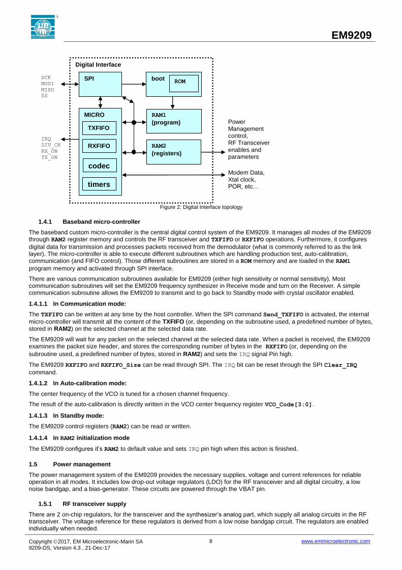
The Digital Interface is shown in Figure 2. It includes:
A four pin Serial Peripheral Interface (SPI).
A Custom Micro-Controller with built in CODEC, FIFO’s and timers.
Two RAMs (Program and Registers).
One ROM and its Boot machine.
The SPI can operate at up to 10MHz (at a typical 25pF load) for reading and writing to the configuration (RAM2) and program
(RAM1) memories.
The Custom Micro-Controller drives an interrupt pin (IRQ) which can be programmed to indicate the status of the EM9209 (e.g.,
that a packet has been sent or received or that auto-calibration has finished). This functionality allows the host controller to
complete other operations or even enter its own low power mode. Additionally, a DIV_CK output pad allows the user to output a
divided version of the internal crystal clock (26MHz). This divided frequency can be disabled or chosen @ 3.25MHz, 325kHz or
32.5kHz. Two other pins, RX_ON and TX_ON, allow the user to command an external PA or/and LNA.
The RAM memories are reset through internal POR on internal VDD_DIG digital supply.
EM9209
Copyright 2017, EM Microelectronic-Marin SA 9209-DS, Version 4.3 , 21-Dec-17
8 www.emmicroelectronic.com
Figure 2: Digital Interface topology
1.4.1 Baseband micro-controller
The baseband custom micro-controller is the central digital control system of the EM9209. It manages all modes of the EM9209 through RAM2 register memory and controls the RF transceiver and TXFIFO or RXFIFO operations. Furthermore, it configures
digital data for transmission and processes packets received from the demodulator (what is commonly referred to as the link layer). The micro-controller is able to execute different subroutines which are handling production test, auto-calibration, communication (and FIFO control). Those different subroutines are stored in a ROM memory and are loaded in the RAM1
program memory and activated through SPI interface.
There are various communication subroutines available for EM9209 (either high sensitivity or normal sensitivity). Most communication subroutines will set the EM9209 frequency synthesizer in Receive mode and turn on the Receiver. A simple communication subroutine allows the EM9209 to transmit and to go back to Standby mode with crystal oscillator enabled.
1.4.1.1 In Communication mode:
The TXFIFO can be written at any time by the host controller. When the SPI command Send_TXFIFO is activated, the internal
micro-controller will transmit all the content of the TXFIFO (or, depending on the subroutine used, a predefined number of bytes, stored in RAM2) on the selected channel at the selected data rate.
The EM9209 will wait for any packet on the selected channel at the selected data rate. When a packet is received, the EM9209 examines the packet size header, and stores the corresponding number of bytes in the RXFIFO (or, depending on the
subroutine used, a predefined number of bytes, stored in RAM2) and sets the IRQ signal Pin high.
The EM9209 RXFIFO and RXFIFO_Size can be read through SPI. The IRQ bit can be reset through the SPI Clear_IRQ
command.
1.4.1.2 In Auto-calibration mode:
The center frequency of the VCO is tuned for a chosen channel frequency.
The result of the auto-calibration is directly written in the VCO center frequency register VCO_Code[3:0].
1.4.1.3 In Standby mode:
The EM9209 control registers (RAM2) can be read or written.
1.4.1.4 In RAM2 initialization mode
The EM9209 configures it’s RAM2 to default value and sets IRQ pin high when this action is finished.
1.5 Power management
The power management system of the EM9209 provides the necessary supplies, voltage and current references for reliable operation in all modes. It includes low drop-out voltage regulators (LDO) for the RF transceiver and all digital circuitry, a low noise bandgap, and a bias-generator. These circuits are powered through the VBAT pin.
1.5.1 RF transceiver supply
There are 2 on-chip regulators, for the transceiver and the synthesizer’s analog part, which supply all analog circuits in the RF transceiver. The voltage reference for these regulators is derived from a low noise bandgap circuit. The regulators are enabled individually when needed.
SPI
RAM1
(program)
RAM2
(registers)
boot
MICRO
SCK
MOSI
MISO
SS
Power Management control, RF Transceiver enables and parameters
IRQ
DIV_CK
RX_ON
TX_ON
codec
timers
TXFIFO
ROM
Digital Interface
RXFIFO
Modem Data, Xtal clock, POR, etc…

EM9209
Copyright 2017, EM Microelectronic-Marin SA 9209-DS, Version 4.3 , 21-Dec-17
9 www.emmicroelectronic.com
1.5.2 Digital supply
A low power regulator generates the supply (VDD_dig) for all digital parts in the system (base-band, frequency synthesizer logic and demodulator). VDD_dig supply is fully internal and this regulator requires no external decoupling capacitor.
1.5.3 Bias generator
The EM9209 features a bias generator that utilizes a temperature compensated on-chip bandgap reference and a calibrated, temperature dependent, PTAT reference current.

EM9209
Copyright 2017, EM Microelectronic-Marin SA 9209-DS, Version 4.3 , 21-Dec-17
10 www.emmicroelectronic.com
2. Pin information
Table 1: EM9209 pinout (die version only)
Bond pad
Name Notes I/O Pin Function Description
1 VSS_DIG 1 Ground Digital Ground
2 VSS_ISO 1 Ground Isolation Ground
3 EN_REG I Digital Input Master chip enable signal
4 VSS_SYNTH 1 Ground Synthesizer Ground
5 VDD_SYNTH Power Output Regulated output voltage of synthesizer supply provided for external decoupling; not to be loaded by any external circuitry
6 VPROG I Prog voltage Programing voltage. This terminal must be left floating
7 RX_ON O Open Drain Digital Output for external LNA
8 TX_ON O Open Drain Digital Output for external PA
9 ANTP 2 I/O RF Positive antenna terminal
10 ANTN 2 I/O RF Negative antenna terminal
11 VBAT Power Input Positive EM9209 supply: connect to 3V battery
12 VSS_RXTX 1 Ground RF Ground
13 VDD_RXTX I Power Output Regulated output voltage of transceiver supply provided for external decoupling; not to be loaded by any external circuitry
14 VSS_RXTX 1 Ground RF Ground
15 XIN I Analog Input Crystal oscillator input
16 XOUT O Analog Output Crystal oscillator output
17 VSS_ISO 1 Ground Insulation Ground
18 DIV_CK O Digital output Programmable Clock output
19 SCK I Digital Input SPI clock input
20 SS I Digital Input SPI Slave Select, active high
21 MOSI I Digital Input SPI data input
22 MISO O Digital output SPI data output
23 VSS_DIG 1 Ground Digital Ground
24 IRQ O Digital Output Interrupt output for external host controller
Note 1: For a proper operation of the chip, this terminal shall be connected to a common ground plane.
Note 2: ANTP and ANTN are internally biased to VDD_RXTX with a typical impedance of 170k Ohm.

EM9209
Copyright 2017, EM Microelectronic-Marin SA 9209-DS, Version 4.3 , 21-Dec-17
11 www.emmicroelectronic.com
3. Electrical specifications
3.1 Handling procedures and absolute maximum ratings
This device has built-in protection against high static voltages or electric fields; however, anti-static precautions must be taken as with any CMOS component. Unless otherwise specified, proper operation can only occur when all terminal voltages are kept within the specified voltage range. Unused inputs must always be tied to a defined logic voltage level.
Table 2: Absolute maximum ratings
Parameter Symbol Min Max Unit
Supply Voltage VBAT - VSS VBAT -0.3 3.8 V
Input Voltage VIN VSS - 0.2 VBAT + 0.2 V
Electrostatic discharge to
Mil-Std-883 method 3015.7
with ref. to VSS_DIG
VESD -1500 +1500 V
Maximum soldering conditions
As per Jedec J-STD-020
Stresses above these listed maximum ratings may cause permanent damage to the device. Exposure beyond specified operating conditions may affect device reliability or cause malfunction
3.2 General operating conditions
Table 3: General operating conditions
Parameter Symbol Min Typ Max Unit
Supply voltage VBAT VBAT 1.9 2.5 3.6 V
Temperature range TA -40 +85 °C
3.3 Electrical characteristics
The electrical characteristics of the EM9209 are summarized in this section. The electrical characteristics are summarized in the following tables.
Unless otherwise specified: VBAT = 1.9V to 3.6V, TA=-40 to +85°C. Typical values are generally stated at room temperature
(T=25oC) with a supply voltage of VBAT = 2.5V.
Table 4: Supply currents on VBAT
Operating mode Notes Symbol Conditions Min Typ Max Unit
Power Down IVBAT_PWDOWN EN_REG = 0 1 A
Standby IVBAT_STDBY 26MHz crystal oscillator disabled 140 A
Auto-calibration IAUTOCAL Auto-calibration mode 4.2 mA
Transmit 1 IVBAT_TX3 POUT = -1.1dBm, 2440 MHz 11 mA
IVBAT_TX7 POUT = 10dBm, 2440 MHz 36 mA
Receive normal sensitivity IVBAT_RXNS 2440 MHz 7 mA
high sensitivity IVBAT_RXHS 2440 MHz 8 mA
Conditions: VBAT = 2.5V.
Note 1: See Table 13 for more detailed PA power settings.

EM9209
Copyright 2017, EM Microelectronic-Marin SA 9209-DS, Version 4.3 , 21-Dec-17
12 www.emmicroelectronic.com
Table 5: DC characteristics
Parameter Symbol Condition Min Typ Max Unit
HIGH level input voltage VIH 0.8 * VBAT VBAT+0.2 V
LOW level input voltage VIL -0.2 0.2 * VBAT V
HIGH level output voltage VOH IOH=100A VBAT-0.3 VBAT V
LOW level output voltage VOL IOL=100A 0 0.3 V
Table 6: RF characteristics
Parameter Conditions Notes Symbol Min Typ Max Unit
General RF conditions
Operating frequency ƒOP 2400 2484 MHz
Differential antenna impedance 200 Ohm
Data rate HS 1.5 2 DR1 1.2 1.5 2 kbps
HS 3 2 DR2 2 3 4 kbps
HS 6 2 DR3 4 6 8 kbps
HS 12 2 DR4 8 12 16 kbps
NS 24 2 DR5 24 kbps
NS 48 2 DR6 48 kbps
NS 72 2 DR7 72 kbps
Channel spacing FCHW 4 MHz
Crystal frequency ƒXTAL 26 MHz
Crystal frequency accuracy 1 ±20 ppm
Transmitter Operation
Output Power Power Level = 7 3,6 PRF7 +10 dBm
Power Level = 6 3,6 PRF6 +9 dBm
Power Level = 5 3,6 PRF5 +6.6 dBm
Power Level = 4 3,6 PRF4 +2.7 dBm
Power Level = 3 3 PRF3 -1.1 dBm
Power Level = 2 3 PRF2 -3.1 dBm
Power Level = 1 3 PRF1 -10.4 dBm
RF power accuracy PRFAC -4 +4 dB
Receiver Operation
Sensitivity for 0.1% BER at room temperature
HS 1.5 4,6 SHS1p5 -115 dBm
HS 3 4,6 SHS3 -113 dBm
HS 6 4,6 SHS6 -111 dBm
HS 12 4,6 SHS12 -107 dBm
NS 24 4,6 SNS24 -100 dBm
NS 48 4,6 SNS48 -98 dBm

EM9209
Copyright 2017, EM Microelectronic-Marin SA 9209-DS, Version 4.3 , 21-Dec-17
13 www.emmicroelectronic.com
Parameter Conditions Notes Symbol Min Typ Max Unit
NS 72 4,6 SNS72 -97 dBm
Maximum input power for 0.1% BER HS 4,5 -10 dBm
NS 4 -10 dBm
Measurement conditions: Load impedance = 100 differential (BALUN type: 2450FB15A0100E 2.45GHZ 1:2BALUN T&R
JOHANSON). Output Power is measured at the output of the BALUN. Reference design available on request.
Note 1: Frequency accuracy includes stability over temperature range and aging of the quartz. Initial correction including the
effect of printed circuit and crystal capacitors, must be stored in the Host in a Non Volatile Memory as a fixed correction to be added on the channel frequency code (see Section 5.2.7).
Note 2: Data rate “on air”. In case of more than 4 consecutive identical symbols, bit stuffing can reduce this data rate from 100%
down to 80% of this value.
Note 3: See Table 13 for more detailed PA power settings.
Note 4: BER (Bit Error Rate) is measured in Transparent mode (see Section 5.2.25) with demodulated data on MISO and fixed
data clock coupled from Data PN15 generator. Because of long preamble (internally fixed at 3 * Address[7:0] byte) used in
EM9209 communication protocol, the PER corresponds to about BER + 3 dB sensitivity.
Note 5: Under certain crystal clock offset conditions and on specific channels, this parameter can be reduced to -35 dBm.
Please ask for the corresponding application note.
Note 6: Data packet loss is inherent to any radio communication system, in particular in the presence of interferers. For specific
applications, it is possible to reduce this packet loss, by selecting a certain data packet configuration and by using a data transfer protocol that tolerates packet errors. For any questions related to packet configuration, please send a message to [email protected] .
Note 7: Depending on the setting of the output power an additional filter of harmonics may be needed to comply with local
regulations. The EM9209 was designed for compliance with the following standards:
1. ETSI EN 300 440-1 V1.6.1
2. ETSI EN 300 328 V1.8.1,
3. FCC Regulations Part 15, §15.247
Customers are however recommended to test compliance of their final systems incorporating or embedding the EM9209 with these or others standards as they may apply and to obtain all necessary licenses and authorizations.
3.4 Timing characteristics
The timings below are requirements for the control software to ensure proper operation.
Table 7: Timing Characteristics
Parameter Notes Symbol Conditions Min Typ Max Unit
Standby mode TX/RX mode 1 tSTDBY_RF 0.8 1 10 ms
Power-down Standby mode tPD_STDBY 1000 s
Auto-calibration tAUTOCAL 340 s
Conditions: VBAT = 2.5V.
Note 1: Dominated by the crystal oscillator start-up time, which strongly depends on the quartz Q-factor. Typical values are for
TSS-3225J, CL=10pF. Maximum is for TSS-3225J with significant margin for Q-factor spreading.

EM9209
Copyright 2017, EM Microelectronic-Marin SA 9209-DS, Version 4.3 , 21-Dec-17
14 www.emmicroelectronic.com
4. Functional modes
4.1 Operational modes
This section describes the operational modes of the EM9209. An example state diagram is given in Figure 3, and each mode is described below. Custom modes are available on special request. The SPI interface is used to set or change the mode by loading and running the corresponding subroutine. Most transitions are immediate, shorter than the SPI transactions, except for
those marked in the figure and listed in Table 7: Timing Characteristics.
Figure 3: Example of state diagram of EM9209 modes
4.1.1 Power down
This mode is enabled when EN_REG terminal is tied to VSS or left floating (internal 3uA pull down). All regulators and the
voltage reference are disabled and supply current on VBAT is in the nA range.
4.1.2 Standby mode
Upon connecting a battery to the VBAT pin and setting the pin EN_REG = VBAT, the regulated digital supply ramps up quickly
(see Table 7). The SPI Register Memory is then set to 0 and the SPI waits the HOST programming. In Standby mode, all internal circuits are disabled and can be accessed, including the crystal oscillator. The host can program the EM9209 for any operational mode at any time.
4.1.3 RAM2 Init mode
The EM9209 is configured through a 16x12 bit RAM memory RAM2. This RAM is reset to 0 when EN_REG signal is set from
VSS to VBAT. In order to avoid 16 SPI Write_RAM2 operations (see Section 5.1.1.9), a dedicated microcontroller subroutine
located at ROM_BOOT_Address = 0 will initialize most RAM2 addresses to their default value.
4.1.4 Auto-calibration modes
VCO center frequency The EM9209 frequency synthesizer has an Auto-calibration mode that must be run periodically by the host. This keeps the channel frequency and FSK modulator operating within specification. Analog components in this block are sensitive to temperature variation, therefore performance may degrade or the link may fail if not run periodically. Typically, Auto-calibration should be run when changing channels or if the operating temperature changes by more than 10 to 20 oC. See Section 5.2.4 for programming details.

EM9209
Copyright 2017, EM Microelectronic-Marin SA 9209-DS, Version 4.3 , 21-Dec-17
15 www.emmicroelectronic.com
PTAT reference current The internally generated PTAT current can be self-calibrated using an internal PTAT generator.
4.1.5 Transmit (TX) mode
In TX mode, the EM9209 outputs a FSK-modulated packet to the antenna pins, returns to Receive mode or to Standby mode
with crystal oscillator enabled and sets the interrupt pin IRQ high. Depending on the chosen subroutine, the EM9209 can either
transmit the whole TXFIFO (till TXFIFO size = 0) or a predefined number of bytes (packet size including the header)
programmed in RAM2.
TX mode is activated from Receive mode or from Standby mode with crystal oscillator enabled using the SPI command Send_TXFIFO.
4.1.6 Receive (RX) mode
In RX mode, the EM9209 is ready to receive a FSK-modulated packet from the antenna. After receiving a packet, the EM9209
sets interrupt pin IRQ high. Depending on the chosen subroutine, the EM9209 can either read the size of the packet to be
received in the packet header or in RAM2 (see Section 5.2.12).

EM9209
Copyright 2017, EM Microelectronic-Marin SA 9209-DS, Version 4.3 , 21-Dec-17
16 www.emmicroelectronic.com
5. User interface
This section describes information the user needs for programming and interfacing the EM9209. The major subsections include the digital interface, the programming interface and register descriptions.
5.1 Digital interface
The EM9209 can be controlled with a 4-wire serial peripheral interface (SPI). The four wires are:
SS: Slave select
SCK: Serial clock
MOSI: Serial data in to EM9209
MISO: Serial data out of EM9209
Details of the SPI interface are provided in Section 5.1.1.
The EM9209 has a programmable interrupt pin (IRQ). The IRQ pin is activated or disabled by the micro-controller.
The EM9209 has 2 programmable open drain type outputs RX_ON and TX_ON in order to connect external PA or LNA. Those
outputs polarity can be set independently.
A more detailed description of setting the IRQ, RX_ON & TX_ON pins is available upon special request.
The EM9209 also has a dedicated DIV_CK output pin to output a divided version of the internal crystal clock (26MHz). This
divided frequency can be disabled or chosen @ 3.25MHz, 325kHz or 32.5kHz (see Section 5.2.5).
All internal enables signals and parameters of the EM9209 are mapped in a small 16x12 bits memory called RAM2. RAM2 can
directly be accessed through SPI and no crystal clock is required. See Section 5.3 for RAM2 mapping description.
5.1.1 SPI operations
The SPI interface is used to read from and to write into all the registers of the EM9209.
SPI operations allow various accesses:
Memories Write and Read actions
Micro-controller commands
Loading of subroutines in RAM1
Test instructions (used in production)
A SPI transaction is defined as all of the activity on SCK, MOSI and MISO that occurs between one rising edge of SS and its next
falling edge (see Figure 4 below). All the data shall be sent starting with the most-significant bit (MSB) first. Not all the commands are encoded on a number of bits multiple of 8. Additional clocks can be sent after the command with no impact on the command decoding. Thus, the chip can be accessed without problems using an 8-bit wide SPI interface.
Each change to MOSI is latched on the rising edge of SCK, and each change to MISO is available on the falling edge of SCK. A
timing diagram is shown in Figure 4. Complete timing specifications are given in Table 8.
Figure 4: SPI timing diagram

EM9209
Copyright 2017, EM Microelectronic-Marin SA 9209-DS, Version 4.3 , 21-Dec-17
17 www.emmicroelectronic.com
Table 8: SPI timing values.
Condition: 25oC, 2.5V, 25pF.
Symbol Parameters Min Max Units
tDS MOSI to SCK Setup 20 ns
tDH SCK to MOSI Hold 20 ns
tSD SS to MISO Valid 30 ns
tCD SCK to MISO Valid 30 ns
tSCKL SCK Low Time 40 ns
tSCKH SCK High Time 40 ns
fSCK SCK Frequency 0 10 MHz
tCS SS to SCK Setup 20 ns
tCH SCK to SS Hold 20 ns
tCSWH SS Inactive Time 20 ns
tCZ SS to MISO High Z 30 ns
5.1.1.1 Status bits: Status[2:0]
For each SPI command, MISO will always give 3 status bits on the first 3 SCK cycles.
As soon as SS goes high, the first status bit (Status[2]) is available on the MISO terminal. This bit is called
“Previous_FIFO_Order_Pending“ and is high when the microcontroller has not yet processed the previous FIFO order.
This process takes a maximum of 8 sck cycles and starts on the falling edge of the SS signal.
Status[1] reflects the inactivity of the crystal oscillator (Status[1] = ‘0’ means the crystal oscillator is running)
Status[0] shows the unlock state of the 2.4GHz LO frequency synthesizer (Status[0] = 0 means the main LO PLL
is locked). For correct transmission operation, status[2:0] must be equal to ‘000’.
The possible SPI actions are described in the following chapters:
5.1.1.2 SPI command: Read_RXFIFO
MOSI 1 1 0 0 x x x x x x x x x x x x
MISO Status[2..0] RXFIFO_Size[4..0] RXFIFO_Data[7..0]
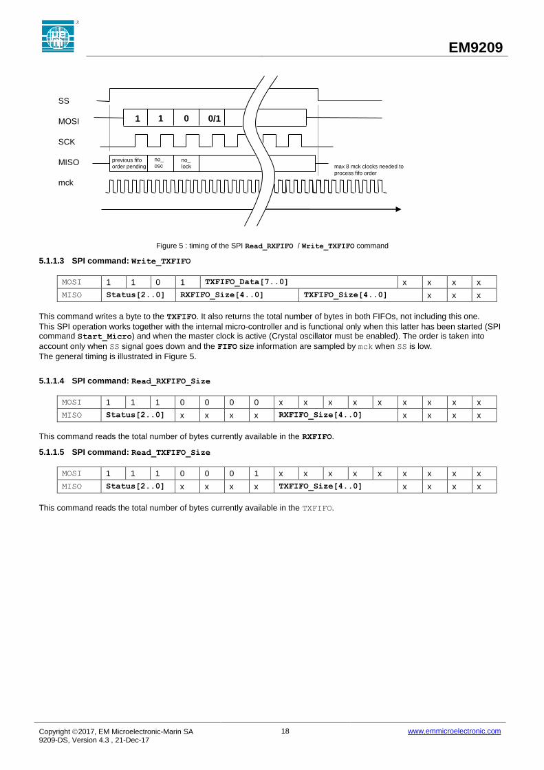
This command returns the next byte out of the RXFIFO. It also returns the total number of bytes currently available in the
RXFIFO (including this one / the one being read).
This SPI operation works together with the internal micro-controller and is functional only when this latter has been started (SPI command Start_Micro) and when the master clock is active (Crystal oscillator must be enabled). The order is taken into
account only when SS signal goes down and the RXFIFO size information are sampled by mck when SS is low.
The general timing is illustrated in Figure 5.
EM9209
Copyright 2017, EM Microelectronic-Marin SA 9209-DS, Version 4.3 , 21-Dec-17
18 www.emmicroelectronic.com
Figure 5 : timing of the SPI Read_RXFIFO / Write_TXFIFO command
5.1.1.3 SPI command: Write_TXFIFO
MOSI 1 1 0 1 TXFIFO_Data[7..0] x x x x
MISO Status[2..0] RXFIFO_Size[4..0] TXFIFO_Size[4..0] x x x
This command writes a byte to the TXFIFO. It also returns the total number of bytes in both FIFOs, not including this one.
This SPI operation works together with the internal micro-controller and is functional only when this latter has been started (SPI command Start_Micro) and when the master clock is active (Crystal oscillator must be enabled). The order is taken into
account only when SS signal goes down and the FIFO size information are sampled by mck when SS is low.
The general timing is illustrated in Figure 5.
5.1.1.4 SPI command: Read_RXFIFO_Size
MOSI 1 1 1 0 0 0 0 x x x x x x x x x
MISO Status[2..0] x x x x RXFIFO_Size[4..0] x x x x
This command reads the total number of bytes currently available in the RXFIFO.
5.1.1.5 SPI command: Read_TXFIFO_Size
MOSI 1 1 1 0 0 0 1 x x x x x x x x x
MISO Status[2..0] x x x x TXFIFO_Size[4..0] x x x x
This command reads the total number of bytes currently available in the TXFIFO.
SS
MOSI
SCK
MISO
mck
previous fifo order pending
no_osc
no_ lock
1 1 0 0/1
max 8 mck clocks needed to
process fifo order

EM9209
Copyright 2017, EM Microelectronic-Marin SA 9209-DS, Version 4.3 , 21-Dec-17
19 www.emmicroelectronic.com
5.1.1.6 SPI command: Read_RAM1
MOSI 0 0 1 address[5..0] x x x x x x x x x x x x x x x
MISO Status[2..0] x x x x x x data_read[11..0] x x x
This command reads the 12-bits word from the specified address (6 bits) of RAM1. This command will put the microcontroller on
hold and reset state, until last bit has been processed.
5.1.1.7 SPI command: Write_RAM1
MOSI 0 0 0 address[5..0] data_write[11..0] x x x
MISO Status[2..0] x x x x x x x x x x x x x x x x x x x x x
This command writes a 12-bits word to the specified address (4 bits) of RAM1. This command will put the microcontroller on hold
and reset state until last bit has been processed.
5.1.1.8 SPI command: Read_RAM2
MOSI 0 1 1 address[3..0] x x x x x x x x x x x x x x x x x
MISO Status[2..0] x x x x data_read[11..0] x x x x x
This command reads the 12-bits word from the specified address (4 bits) of RAM2. This command will put the microcontroller on
hold until last bit has been processed.
5.1.1.9 SPI command: Write_RAM2
MOSI 0 1 0 address[3..0] data_write[11..0] x x x x x
MISO Status[2..0] x x x x x x x x x x x x x x x x x x x x x
This command writes a 12-bits word to the specified address (4 bits) of RAM2. This command will put the microcontroller on hold
until last bit has been processed.
5.1.1.10 SPI command: Reset_Micro
MOSI 1 1 1 0 0 1 0 x
MISO Status[2..0] x x x x x
This instruction allows an asynchronous reset of the microcontroller. Never use this command when the Micro is running (RAM2 and FIFO’s content could be corrupted). Always first stop the Micro using SPI command Stop_Micro prior to use
Reset_Micro.
5.1.1.11 SPI command: Stop_Micro
MOSI 1 1 1 0 0 1 1 x
MISO Status[2..0] x x x x x
This command stops the micro-controller.
5.1.1.12 SPI command: Start_Micro
MOSI 1 1 1 0 1 0 0 x
MISO Status[2..0] x x x x x
This command starts the micro-controller and executes the program currently stored in RAM1.
5.1.1.13 SPI command: Clear_IRQ
MOSI 1 1 1 0 1 0 1 x
MISO Status[2..0] x x x x x
Use this command to reset the IRQ signal. It works only when micro-controller is running.

EM9209
Copyright 2017, EM Microelectronic-Marin SA 9209-DS, Version 4.3 , 21-Dec-17
20 www.emmicroelectronic.com
5.1.1.14 SPI command: Send_TXFIFO
MOSI 1 1 1 0 1 1 0 x
MISO Status[2..0] x x x x x
This command will send the current contents of the TXFIFO. Depending on the selected subroutine, the program either sends
the full content of the FIFO, or the number of bytes specified in RAM2.
5.1.1.15 SPI command: Aux_com
MOSI 1 1 1 0 1 1 1 x
MISO Status[2..0] x x x x x
This command allows the Channel RSSI to be read and stored to Limit_RSSI[3:0].
5.1.1.16 SPI command: ROM_Boot
MOSI 1 1 1 1 0 0 0 ROM_Boot_Address[8..0]
MISO Status[2..0] x x x x x x x x x x x x x
This command copies the 64 12-bits instructions from the specified ROM address to RAM1. This allows for fast initialization of the
micro-controller subroutines. The crystal oscillator must be enabled to perform this operation. Additionally, ROM_Boot command stops and resets the micro-
controller.
5.1.1.17 SPI command: ROM_Boot0_and_Start
MOSI 1 1 1 1 1 1 1 x
MISO Status[2..0] x x x x x
This command copies the 64 12-bits instructions from the ROM address 0 to RAM1. This allows for fast initialization of the micro-
controller subroutines. The crystal oscillator must be enabled to perform this operation. Additionally, ROM_Boot0_and_Start command resets and
starts the micro-controller.

EM9209
Copyright 2017, EM Microelectronic-Marin SA 9209-DS, Version 4.3 , 21-Dec-17
21 www.emmicroelectronic.com
5.2 Programming interface
The Programming interface section describes how to program the EM9209 by writing to the EM9209 RAM2 or by booting and
running in ROM stored subroutines. The complete RAM2 description can be found in Section 5.3.
5.2.1 RAM2, RAM1 reset
The EM9209 automatically performs a power on reset to RAM1, RAM2 when internal VDD_DIG voltage is established (after
EN_REG terminal is set to VBAT from VSS) see Section 3.4 for minimal timing.
After reset, all RF communication setup parameters (RF channel, etc.) must be reconfigured (see Section 5.2.2), and the PLL auto-calibration cycle must be initiated again.
5.2.2 RAM2 Initialization
The EM9209 has a dedicated subroutine located at the ROM_Boot_Address = 0 which will initialize the RAM2 memory to its
default state (see Section 5.3). To request the RAM2 initialization, EN_REG terminal must be enabled. VDD_SYNTH, VDD_RXTX regulators and crystal
oscillator must be started by writing “111000000100” in the RAM2 at the address 0 (see Section 5.1.1.9). Quartz activity can be
monitored through Status[1] (see Section 5.1.1.1) by using a simple Stop_Micro SPI command, for example. When
Status[1] has gone low, the RAM2 initialization subroutine can be executed. This is achieved by the SPI command ROM_Boot
described in Section 5.1.1.16 with argument ROM_Boot_Address = 0.
There are then 2 possibilities to start the subroutine: Manual Boot (only RAM2 initialization subroutine is executed):
In this case, the ROMboot instruction of the microcontroller must be disabled. Use SPI command Write_RAM1 with address
= 13 and data_write = 1184 (this will initialize RAM2 with RB_Inst_Dis = 1, see Section 5.2.27).
Use then the SPI command Start_Micro described in Section 5.1.1.12.The end of initialization will be signaled with IRQ
going high. SPI command Clear_IRQ (see Section 5.1.1.13) allows clearing the interrupt.
Automatic Boot (Following in ROM chained subroutines will be successively booted and executed):
Use then the SPI command Start_Micro described in Section 5.1.1.12. In this case, RAM2 initialization subroutine is
executed and following subroutines will be automatically booted and executed. The default chain stored in ROM is:
RAM2 Initialization(located @ ROM_Boot_Address = 0)
Internal PTAT current value auto-calibration(located @ ROM_Boot_Address = 33)
VCO code auto-calibration on center band frequency (2440 MHz) (located @ ROM_Boot_Address = 64)
High Sensitivity Communication Subroutine with payload defined in RAM2 (located @ ROM_Boot_Address = 128).
Note 1: Using SPI short command ROM_Boot0_and_Start will also result in Automatic Boot.
5.2.3 Internal PTAT current auto-calibration
This auto-calibration is used to calibrate the current delivered by the internal PTAT generator (Proportional To Absolute Temperature). To load the auto-calibration in RAM1 memory, EN_REG terminal must be enabled. VDD_SYNTH, VDD_RXTX regulators must be
enabled and crystal oscillator must be running (see Section 5.2.2). Use then the SPI command ROM_Boot (Section 5.1.1.16 )
with argument ROM_Boot_Address = 33 (location of the auto-calibration subroutine in the ROM).
There are then 2 possibilities to start the subroutine: Manual Boot (only internal PTAT current value auto-calibration subroutine is executed):
Set the ROOMBOOT instruction disable bit RB_Inst_Dis = 1 using SPI command Write_RAM2 (see Section 5.2.27). If
RB_Inst_Dis has been previously set = 1, this step can be omitted. Use then the SPI command Start_Micro described in
Section 5.1.1.12.The end of auto-calibration will be signaled with IRQ going high. SPI command Clear_IRQ (see Section
5.1.1.13) allows clearing the interrupt. Automatic Boot (Following in ROM chained subroutines will be successively booted and executed):
Set the ROOMBOOT instruction disable bit RB_Inst_Dis = 0 using SPI command Write_RAM2 (see Section 5.2.27). If
RB_Inst_Dis has been previously set = 0, this step can be omitted. Use then the SPI command Start_Micro described in
Section 5.1.1.12. In this case, internal PTAT current value auto-calibration subroutine is executed and following chained subroutines will be automatically booted and executed. The default chain stored in ROM is:
Internal PTAT current value auto-calibration(located @ ROM_Boot_Address = 33)
VCO code auto-calibration on center band frequency (2440 MHz) (located @ ROM_Boot_Address = 64)
High Sensitivity Communication Subroutine with payload defined in RAM2 (located @ ROM_Boot_Address = 128).
The calibration of the PTAT is independent of the temperature and only needs to be executed once when the chip is powered. Because this value should be constant during product life, it is possible to do calibration only once and to store RAM2@5<3:0>
value somewhere in a non-volatile memory. Write_RAM2 SPI command with this pre-stored value could then be used to set the
correct internal PTAT current.

EM9209
Copyright 2017, EM Microelectronic-Marin SA 9209-DS, Version 4.3 , 21-Dec-17
22 www.emmicroelectronic.com
5.2.4 VCO code auto-calibration
This auto-calibration is used to calibrate the analog circuits of the PLL. For correct transmission and reception, the PLL should be calibrated at each channel frequency to be used before the link is established or if the operating temperature changes by more than 10 to 20 oC. To load the auto-calibration in RAM1 memory, EN_REG terminal must be enabled. VDD_SYNTH, VDD_RXTX regulators must be
enabled and crystal oscillator must be running (see Section 5.2.2). Use then the SPI command ROM_Boot (Section 5.1.1.16 )
with argument ROM_Boot_Address = 64 (location of the auto-calibration subroutine in the ROM).
Auto-calibration frequency is set trough register VcoCalibFreq[11:0] which is located in RAM1 at the address 53 (default
value of VcoCalibFreq[7:0] = 128 when VCO frequency auto-calibration subroutine is loaded). It must be programmed
through the SPI Write_RAM1 command to fit the required frequency operation. VcoCalibFreq[11:0] is:
VcoCalibFreq[7:0] = (round(4’259’840 / Fo) – 1’618); where Fo is the RF operating frequency in MHz.
VcoCalibFreq[11:8] = ”1011”.
Examples: Fo = 2480, hex VcoCalibFreq[11:0] = ‘B64’.
Fo = 2440, hex VcoCalibFreq[11:0] = ‘B80’.
Fo = 2400, hex VcoCalibFreq[11:0] = ‘B9D’.
See table 12 below. There are then 2 possibilities to start the subroutine:
Manual Boot (only VCO code auto-calibration subroutine is executed):
Set the ROOMBOOT instruction disable bit RB_Inst_Dis = 1 using SPI command Write_RAM2 (see Section 5.2.27). If
RB_Inst_Dis has been previously set = 1, this step can be omitted. Use then the SPI command Start_Micro described in
Section 5.1.1.12.The end of initialization will be signaled with IRQ going high. SPI command Clear_IRQ (see Section
5.1.1.13) allows clearing the interrupt. Automatic Boot (Following in ROM chained subroutines will be successively booted and executed):
Set the ROOMBOOT instruction disable bit RB_Inst_Dis = 0 using SPI command Write_RAM2 (see Section 5.2.27). If
RB_Inst_Dis has been previously set = 0, this step can be omitted. Use then the SPI command Start_Micro described in
Section 5.1.1.12. In this case, VCO code auto-calibration subroutine is executed and following chained subroutines will be automatically booted and executed. The default chain stored in ROM is:
VCO code auto-calibration on chosen frequency (located @ ROM_Boot_Address = 64)
High Sensitivity Communication Subroutine with payload defined in RAM2 (located @ ROM_Boot_Address = 128).
In both manual and automatic Boot, the end of the VCO code auto-calibration routine will be signaled with IRQ going high. SPI
command Clear_IRQ (see Section 5.1.1.13) allows clearing the interrupt.
The calibration of the PLL may vary if the external conditions change (e.g., temperature), therefore calibration should be repeated periodically.
5.2.5 External Clock frequency (on DIV_CK terminal)
The Frequency of the optional clock output can be set through the register Ck_Pad[1:0]( RAM2@0[4:3] ) as shown in Table
9.
Table 9: Ck_Pad Frequencies
Control Bits Ck_Pad[1:0]
Clock Frequency on
Div_Ck Output
‘00’ no clock
‘01’ 3.25 MHz
‘10’ 325 kHz
‘11’ 32.5 kHz

EM9209
Copyright 2017, EM Microelectronic-Marin SA 9209-DS, Version 4.3 , 21-Dec-17
23 www.emmicroelectronic.com
5.2.6 Channel Data rate
The EM9209 has a programmable channel data rate of 1.5kbps to 72kbps for transmission and reception in normal sensitivity mode. The channel data rate is set by R_Bit_Clk[8:0] (RAM2@12[8:0]) and Ch_Rate[2:0] (RAM2@12[11:9]) as shown
in Table 10. The complete typical values RAM2@12[11:0] is also reported. In high sensitivity mode, only the 4 slower data
rates are available (Ch_Rate[2:0] = ‘000’ to ‘011’).
Table 10: Channel Data Rate
On air bit rate [kbps]
Ch_Rate[2:0] R_Bit_Clk[8:0] RAM2@12[11:0]
[hex]
1.5 ‘000‘ ‘110000000’ 0x180
2.99 ‘001’ ‘011000000’ 0x2C0
6.02 ‘010’ ‘001011111’ 0x45F
12.037 ‘011’ ‘000101111’ 0x62F
24.074 ‘100’ ‘000010111’ 0x817
48.15 ‘101’ ‘000001011’ 0xA0B
72.22 ‘110’ ‘000000111’ 0xC07
The exact recovered and transmitted bit rate is given by:
On-air bit rate = fref / 45 / (unsigned(R_Bit_Clk[8:0] )+1) [bit/sec], with fref = 26MHz.
Conversely, the R_Bit_Clk[8:0]register value is defined as:
R_Bit_Clk[8:0] = (fref / (45 * On air bit rate)) – 1, with fref = 26MHz.
To establish a communication, both linked devices must be set to the same data rate.
In high-sensitivity mode, the on-air bit rate can be increased or decreased around the center data rate defined by Ch_Rate[2:0], by selecting R_Bit_Clk[8:0] values, as shown in figure below.
1.5kbps
000
3kbps
001
6kbps
010
12kbps
011
2kbps 4kbps 8kbps 16kbps
Ch-Rate[2..0]
1.2kbps
Sensitivity
[dBm]
-115
Air datarate
R_Bit_Clk[8:0]
-111
-113
-107
-98
-102
-96
High Sensitivity modes
24kbps
100
48kbps
101
72kbps
110
Normal Sensitivity modes
Figure 6 : On-air data rate selection
EM9209
Copyright 2017, EM Microelectronic-Marin SA 9209-DS, Version 4.3 , 21-Dec-17
24 www.emmicroelectronic.com
5.2.7 RF Frequency of operation
The channel register sets the center frequency of the transmission channel used by the EM9209. The channel is set by the Frequ[16:0]register. The RF center frequency is defined as:
Frequency should be between 2400MHz and 2484MHz
Frequency = fref * (92 + unsigned( Frequ[16..0] ) / 2^15), with fref = 26MHz.
Conversely, the Frequ[16:0]register value is defined as:
Frequ[16..0] = (Frequency * 2^15 / fref) – 92, with fref = 26MHz.
The channel step is given by 26MHz / 32768 and is approximately equal to 793Hz.
The RF frequency must be corrected to compensate the initial crystal oscillator deviation. After printed circuit board assembly and frequency measurement, a value must be stored in the Host in a Non Volatile Memory as a fixed correction to be added on the channel frequency code.
To establish a communication, both linked devices must be set to the same channel. The host can program a channel change,
which is validated when SPI signal SS goes down.
Channel spacing of 4 MHz is recommended to limit interference with other EM9209 devices operating on adjacent channels. The table below describes a possible definition of the channels.
Table 11: Channel Frequency Selection
Channel Frequency [MHz]
Frequ[16:5]
[hex]
Frequ[4:0]
[hex]
VcoCalibFreq
[11:0] [hex]
0 2401.5 0x176 0x04 0xB9C
1 2405.5 0x213 0x16 0xB99
2 2409.5 0x2B1 0x07 0xB96
3 2413.5 0x34E 0x18 0xB93
4 2417.5 0x3EC 0x09 0xB90
5 2421.5 0x489 0x1B 0xB8D
6 2425.5 0x527 0x0C 0xB8A
7 2429.5 0x5C4 0x1D 0xB87
8 2433.5 0x662 0x0E 0xB84
9 2437.5 0x700 0x00 0xB82
10 2441.5 0x79D 0x11 0xB7F
11 2445.5 0x83B 0x02 0xB7C
12 2449.5 0x8D8 0x13 0xB79
13 2453.5 0x976 0x04 0xB76
14 2457.5 0xA13 0x16 0xB73
15 2461.5 0xAB1 0x07 0xB71
16 2465.5 0xB4E 0x18 0xB6E
17 2469.5 0xBEC 0x09 0xB6B
18 2473.5 0xC89 0x1B 0xB68
19 2477.5 0xD27 0x0C 0xB65
5.2.8 Address Byte
For proper communication between two devices, the receiving device must set the Address[7:0] register to match the
transmitting device’s Address[7:0] register.
The Address byte is used in the packet preamble in order to set the byte start in the bit to byte built-in reconstruction algorithm. Decimal value of Address[7:0] must be different from 0, 48, 51, 99, 102, 146, 153, 204. To prevent wrong packet
synchronization when address rx and tx differ by a right or left shift, even address values must be avoided and the most-significant bit (MSB) of the first payload byte should be the invert of the address most-significant bit (MSB).
As the preamble to start packet detection consists of three successive address bytes, the reception can be triggered by a payload containing such data, even if the transmit and receive addresses are not equal. For applications where the integrity of the address or the payload is critical, it is recommended to include CRC or error correction bits inside the payload.

EM9209
Copyright 2017, EM Microelectronic-Marin SA 9209-DS, Version 4.3 , 21-Dec-17
25 www.emmicroelectronic.com
5.2.9 Bit stuffing
To improve the receiver’s clock recovery, the data transmitted is automatically bit stuffed with a hardwired algorithm. The internal bit stuffing procedure is allowing a maximum of 4 consecutive same symbols to be transmitted. It corresponds to a minimum efficiency of 80%, or a minimum bit rate described by Table 12.
Table 12: “On air” versus Minimum Bit stuffed Data Rates
On air bit rate [kbps]
Minimum bit stuffed data rate [kbps]
1.5 1.2
3 2.4
6 4.8
12 9.6
24 19.2
48 38.4
72 57.6
5.2.10 TX power level
The PA output power can be adjusted to many different levels from -20dBm to +10 dBm with different efficiencies.
Table 13 shows 8 typical levels with optimum efficiency. These levels are set by I_Pre_PA[4:0] and I_PA[4:0] register
bits. Typical current consumption and PA efficiency for each of these power levels are also shown.
Table 13: RF power settings for the EM9209
Power Level I_Pre_PA[4:0]
[unsigned decimal]
I_PA[4:0]
[unsigned decimal]
Output
Power
[dBm]
PA Power efficiency
[%]
DC total Current
Consumption
[mA]
7 29 18 +10 27.3 36.3
6 21 5 +9.3 29.7 29.5
5 10 2 +6.6 24.2 20,7
4 7 1 +2.7 15.8 14.4
3 4 1 -1.1 9.4 11.2
2 3 1 -3.1 7 10.2
1 1 1 -10.4 1.9 8.1
Measurement conditions: 72kbps, f0=2440MHz, VBAT = 2.45V, VSS=0V, T=25 °C, load impedance = 100 differential (BALUN type: 2450FB15A0100E 2.45GHZ 1:2BALUN T&R JOHANSON), other RAM2 parameters set to default values. Output
Power is measured at the output of the BALUN.
5.2.11 External PA and LNA control
A control signal for an external Power Amplifier or low noise Amplifier is available if a higher transmit output power is required
than the EM9209 can output or when a higher sensitivity is needed. The TX_ON & RX_ON pins provide open drains controlled
through the internal software. It is possible to control the polarity by programming the RAM1 memory accordingly. Inverted
polarity can be obtained on special request. When using an external Power Amplifier, the user is requested to comply with all ISM band regulations.
5.2.12 Packet (TX and RX) payload
5.2.12.18 Mode payload size in the header:
In this mode (defined by the SPI Command ROM_Boot @256 or 320), the transmit payload can be up to 31 bytes. A header
byte which defines the packet size is added (See Section 6). The payload (and header) are read and written through the SPI command Read_RXFIFO and Write_TXFIFO (See Section 5.1.1).

EM9209
Copyright 2017, EM Microelectronic-Marin SA 9209-DS, Version 4.3 , 21-Dec-17
26 www.emmicroelectronic.com
5.2.12.19 Mode payload size in RAM2:
In this mode (defined by the ROM_Boot @128 or 192), the transmit payload can be up to 32 bytes, but the first byte following
the Address byte has to be different from Address[7:0]. Payload size is defined in the register N_Pay[4:0]
(RAM2@14[4:0]). The payload is read and written through the SPI command Read_RXFIFO and Write_TXFIFO (See Section
5.1.1).
5.2.13 Registers: TXFIFO and RXFIFO
The EM9209 has two 32 Bytes FIFO’s (TXFIFO and RXFIFO). The transmit TXFIFO can be accessed through the SPI
command Write_TXFIFO. The receive RXFIFO can be accessed through the SPI command Read_RXFIFO.
The transmit FIFO must be loaded prior to transmission. The size of the transmit TXFIFO is monitored at each write FIFO
command or can be viewed at any time through the command Read_TXFIFO_Size (see Section 5.1.1.5).
The receive RXFIFO can be read after an incoming packet has been received. The size of the receive RXFIFO is monitored at
each Read_FIFO command or can be viewed at any time through the command Read_RXFIFO_Size (see Section 5.1.1.4).
Note: Both TXFIFO and RXFIFO are managed by the microcontroller, which means that this latter must be enabled
(Start_Micro) and running (crystal oscillator enabled, Status[1] = ‘0’). Also, the SPI command Reset_Micro will reset all
internal TXFIFO and RXFIFO pointers to 0.
5.2.14 Transmission flow, “high sensitivity”, mode payload defined in RAM2, quick control (automatic ROMboot).
This section describes the entire flow for transmitting data on the EM9209 in high sensitivity mode (whole TXFIFO is
transmitted):
1. Start the EM9209 by setting EN_REG terminal equal to VBAT.
2. Perform a first RAM2 initialization:
a. Start both VDD_SYNTH and VDD_RXTX regulators + crystal oscillator by writing (SPI command Write_RAM2)
“111000000100” in RAM2@0 (see Section 5.1.1.9).
b. Wait 1 to 10ms for the crystal to start. Oscillator activity can be poled trough Status[1] (see Section 5.2.2).
c. Use the SPI command ROM_Boot0_and_Start (see Section 5.1.1.17). EM 9209 will set default initialization
parameters, auto calibrate internal PTAT and VCO on 2440 MHz band, set IRQ pin high and boot the
Communication subroutine located at ROM_BOOT_address = 128.
d. Use the SPI command Clear_IRQ (see Section 5.1.1.13) to clear the interrupt.
3. Write the TXFIFO through SPI Write_TXFIFO (see Section 5.1.1.3).
4. Use SPI Send_TXFIFO command to transmit the packet.
5. The EM9209 will:
a. Send the Packet with payload size defined in RAM2.
b. Set the IRQ pin high when transfer is complete.
6. User can reset the IRQ signal by using the SPI command Clear_IRQ.
7. Next Packet transmission only implies steps 3 to 6 to be repeated.
Note 1: The Data Bit Rate, transmit power and carrier frequency are the default values defined in Section 5.3. Use SPI
command Write_RAM2 to redefine those parameters if needed.
Note 2: Transmission mode is started from reception mode. So, it is not possible to exclude that an incoming packet has
triggered the IRQ before Sent Packet IRQ is activated (IRQ is the same for all operational modes). The SPI command
Read_TXFIFO_Size and Read_RXFIFO_Size allows the user to look at both TXFIFO and RXFIFO to determine the origin of
the interruption.
Note 3: Transmission mode is operated by the internal microcontroller, which operates by taking control of RAM2 and TXFIFO.
Read and Write SPI accesses to RAM2 will put the microcontroller on hold. If the SPI transaction time is too long (if SCK
frequency is close to channel data rate), correct transmission operation can be corrupted.SPI commands to retrieve RAM2
values such as Limit_RSSI[3:0] or DFT_Mes[7:0] should be sent immediately after IRQ signal has gone high rather
than after a Send_TXFIFO request.
5.2.15 Reception flow, “high sensitivity”, mode payload defined in RAM2, quick control (automatic ROMboot).
This section describes the entire flow for receiving data on the EM9209 in high sensitivity mode with payload size defined in header:
1. Start the EM9209 by setting EN_REG terminal equal to VBAT.
2. Perform a first RAM2 initialization:

EM9209
Copyright 2017, EM Microelectronic-Marin SA 9209-DS, Version 4.3 , 21-Dec-17
27 www.emmicroelectronic.com
a. Start both VDD_SYNTH and VDD_RXTX regulators + crystal oscillator by writing (SPI command Write_RAM2)
“111000000100” in RAM2@0 (see Section 5.1.1.9).
b. Wait 1 to 10ms for the crystal to start. Oscillator activity can be poled trough Status[1] (see Section 5.1.1.1).
c. Use the SPI command ROM_Boot0_and_Start (see Section 5.1.1.17). EM9209 will set default initialization
parameters, auto calibrate internal PTAT and VCO on 2440 MHz band, set IRQ pin high and boot the
Communication subroutine located at ROM_BOOT_address = 128.
d. Use the SPI command Clear_IRQ (see Section 5.1.1.13) to clear the interrupt.
3. The EM9209 will:
a. Wait an incoming Packet with payload size defined in RAM2 and store it in the RXFIFO (including the header).
b. Set the IRQ pin high when packet has been stored in the RXFIFO.
4. User can reset the IRQ signal by using the SPI command Clear_IRQ.
5. User can read the RXFIFO using the SPI command Read_RXFIFO (see Section 5.1.1.2).
Note 1: The Data Bit Rate, transmit power and carrier frequency are the default values defined in Section 5.3. Use SPI
command Write_RAM2 to redefine those parameters if needed.
Note 2: Reception mode is operated by the internal microcontroller, which operates by taking control of RAM2 and TXFIFO.
Read and Write SPI accesses to RAM2 will put the microcontroller on hold. If the SPI transaction time is too long (if SCK
frequency is close to channel data rate), correct transmission operation can be corrupted.SPI commands to retrieve RAM2
values such as Limit_RSSI[3:0] or DFT_Mes[7:0] should be sent immediately after IRQ signal has gone high.
5.2.16 Transmission flow, “high sensitivity”, mode entire TXFIFO, manual control (step by step).
This section describes the entire flow for transmitting data on the EM9209 in high sensitivity mode (whole TXFIFO is
transmitted):
1. Start the EM9209 by setting EN_REG terminal equal to VBAT.
2. Perform a first RAM2 initialization:
a. Start both VDD_SYNTH and VDD_RXTX regulators + crystal oscillator by writing (SPI command Write_RAM2)
“111000000100” in RAM2@0 (see Section 5.1.1.9).
b. Wait 1 to 10ms for the crystal oscillator to start. Oscillator activity can be poled trough Status[1] (see Section
5.1.1.1).
c. Use the SPI command ROM_Boot with ROM_Boot_Address = 0 (see Section 5.1.1.16).
d. Use SPI command Write_RAM1 with address = 13 and data_write = 1184 (to set RB_Inst_Dis = 1, see Section
5.2.27).
e. Use the SPI command Start_Micro (see Section 5.1.1.12).
f. Wait the interrupt IRQ signal to go high (this will mean that crystal oscillator has started and that RAM2 initialization
subroutine has been executed).
g. Clear IRQ using the SPI command Clear_IRQ (see Section 5.1.1.13).
3. Perform a PTAT auto-calibration sequence:
a. Use the SPI command ROM_Boot with ROM_Boot_Address = 33.
b. Use the SPI Start_Micro command.
c. Wait the interrupt IRQ signal to go high (this will mean that PTAT auto-calibration subroutine has been executed).
d. Clear IRQ using the SPI command Clear_IRQ.
4. Use SPI write RAM2 command to configure:
a. The data rate (R_Bit_Clk[8:0] (and Ch_Rate[2:0] for normal sensitivity), see Section 5.2.6 ).
b. The output power (I_Pre_PA[4:0] and I_PA[4:0], see Section 5.2.10).
c. The Address byte Address[7:0] (see Section 5.2.8).
d. The channel frequency Frequ[16:0] (see Section 5.2.7).
5. Perform a VCO auto-calibration sequence:
a. Use the SPI command ROM_Boot with ROM_Boot_Address = 64.
b. Program the center frequency for the auto-calibration via SPI command Write_RAM1 (see Section 5.2.4)
c. Use the SPI Start_Micro command.

EM9209
Copyright 2017, EM Microelectronic-Marin SA 9209-DS, Version 4.3 , 21-Dec-17
28 www.emmicroelectronic.com
d. Wait the interrupt IRQ signal to go high (this will mean that VCO auto-calibration subroutine has been executed).
e. Clear IRQ using the SPI command Clear_IRQ.
6. Boot high sensitivity communication software
a. Use SPI command ROM_Boot with ROM_Boot_Address = 256.
b. Start the microcontroller with the SPI command Start_Micro
7. Write the TXFIFO through SPI Write_TXFIFO (see Section 5.1.1.3). The first byte written is the header and contents
the payload size in its 5 LSBs.
8. Use SPI Send_TXFIFO command to transmit the packet.
9. The EM9209 will:
a. Send the Packet until TXFIFO is empty.
b. Set the IRQ pin high when transfer is complete.
10. User can reset the IRQ signal by using the SPI command Clear_IRQ.
11. Next Packet transmission only implies steps 7 to 9 to be repeated.
Note 1: Transmission mode is started from reception mode. So, it is not possible to exclude that an incoming packet has
triggered the IRQ before Sent Packet IRQ is activated (IRQ is the same for all operational modes). The SPI command
Read_TXFIFO_Size and Read_RXFIFO_Size allows the user to look at both TXFIFO and RXFIFO to determine the origin of
the interruption.
Note 2: Transmission mode is operated by the internal microcontroller, which operates by taking control of RAM2 and TXFIFO.
Read and Write SPI accesses to RAM2 will put the microcontroller on hold. If the SPI transaction time is too long (if SCK
frequency is close to channel data rate), correct transmission operation can be corrupted.SPI commands to retrieve RAM2
values such as Limit_RSSI[3:0] or DFT_Mes[7:0] should be sent immediately after IRQ signal has gone high rather
than after a Send_TXFIFO request.
5.2.17 Reception flow, “high sensitivity”, mode payload size in header, manual control (step by step).
This section describes the entire flow for receiving data on the EM9209 in high sensitivity mode with payload size defined in header:
1. Start the EM9209 by setting EN_REG terminal equal to VBAT.
2. Perform a first RAM2 initialization:
a. Start both VDD_SYNTH and VDD_RXTX regulators + crystal oscillator by writing (SPI command Write_RAM2)
“111000000100” in RAM2@0 (see Section 5.1.1.9).
b. Wait 1 to 10ms for the crystal oscillator to start. Oscillator activity can be poled trough Status[1] (see Section
5.1.1.1).
c. Use the SPI command ROM_Boot with ROM_Boot_Address = 0 (see Section 5.1.1.16).
d. Use SPI command Write_RAM1 with address = 13 and data_write = 1184 (to set RB_Inst_Dis = 1, see Section
5.2.27).
e. Use the SPI command Start_Micro (see Section 5.1.1.12).
f. Wait the interrupt IRQ signal to go high (this will mean that crystal oscillator has started and that RAM2 initialization
subroutine has been executed).
g. Clear IRQ using the SPI command Clear_IRQ (see Section 5.1.1.13).
3. Perform a PTAT auto-calibration sequence:
a. Use the SPI command ROM_Boot with ROM_Boot_Address = 33.
b. Use the SPI Start_Micro command.
c. Wait the interrupt IRQ signal to go high (this will mean that PTAT auto-calibration subroutine has been executed).
d. Clear IRQ using the SPI command Clear_IRQ.
4. Use SPI write RAM2 command to configure:
a. The data rate (R_Bit_Clk[8:0] (and Ch_Rate[2:0] for normal sensitivity), see Section 5.2.6 ).
b. The output power (I_Pre_PA[4:0] and I_PA[4:0], see Section 5.2.10).
c. The Address byte Address[7:0] (see Section 5.2.8).
d. The channel frequency Frequ[16:0] (see Section 5.2.7).
5. Perform a VCO auto-calibration sequence:

EM9209
Copyright 2017, EM Microelectronic-Marin SA 9209-DS, Version 4.3 , 21-Dec-17
29 www.emmicroelectronic.com
a. Use the SPI command ROM_Boot with ROM_Boot_Address = 64.
b. Program the center frequency for the auto-calibration via SPI command Write_RAM1 (see Section 5.2.4).
c. Use the SPI Start_Micro command.
d. Wait the interrupt IRQ signal to go high (this will mean that VCO auto-calibration subroutine has been executed).
e. Clear IRQ using the SPI command Clear_IRQ.
6. Boot high sensitivity communication software
a. Use SPI command ROM_Boot with ROM_Boot_Address = 256.
b. Start the microcontroller with the SPI command Start_Micro
7. The EM9209 will:
a. Wait an incoming Packet and store the number of byte stored in the header in the RXFIFO (including the header).
b. Set the IRQ PIN high when packet has been stored in the RXFIFO.
8. User can reset the IRQ signal by using the SPI command Clear_IRQ.
9. User can read the RXFIFO using the SPI command Read_RXFIFO (see Section 5.1.1.2).
Note 1: Reception mode is operated by the internal microcontroller, which operates by taking control of RAM2 and TXFIFO.
Read and Write SPI accesses to RAM2 will put the microcontroller on hold. If the SPI transaction time is too long (if SCK
frequency is close to channel data rate), correct transmission operation can be corrupted.SPI commands to retrieve RAM2
values such as Limit_RSSI[3:0] or DFT_Mes[7:0] should be sent immediately after IRQ signal has gone high.
5.2.18 Transmission flow, “high sensitivity”, mode payload size defined in RAM2
This section describes the entire flow for transmitting data on the EM9209 in high sensitivity mode with payload size defined in RAM2.
The steps are the same as described in Section 5.2.16, excepted:
The Payload size N_Pay[4:0] must be defined after step 4.
The header byte no longer defines the number of byte of the payload.
The ROM_Boot_Address must be set to 128 in step 6.
5.2.19 Reception flow, “high sensitivity”, mode payload size defined in RAM2
This section describes the entire flow for receiving a packet with the EM9209 in high sensitivity mode, with payload size defined in RAM2.
The steps are the same as described in Section 5.2.17, excepted:
The Payload size N_Pay[4:0] must be defined after step 4.
The header byte no longer defines the number of byte of the payload.
The ROM_Boot_Address must be set to 128 in step 6.
5.2.20 Transmission flow, “normal sensitivity”, mode entire TXFIFO
This section describes the entire flow for transmitting data on the EM9209 in normal sensitivity mode (whole TXFIFO is
transmitted):
The steps are the same as described in Section 5.2.16, excepted:
The ROM_Boot_Address must be set to 320 in step 6.
5.2.21 Reception flow, “normal sensitivity”, mode payload size in header
This section describes the entire flow for receiving a packet with the EM9209 in normal sensitivity mode, with payload size defined in header.
The steps are the same as described in Section 5.2.17, excepted:
The ROM_Boot_Address must be set to 320 in step 6.
5.2.22 Transmission flow, “normal sensitivity”, mode payload size defined in RAM2
This section describes the entire flow for transmitting data on the EM9209 in normal sensitivity mode with payload size defined in RAM2.
The steps are the same as described in Section 5.2.16, excepted:
The Payload size N_Pay[4:0] must be defined after step 4.

EM9209
Copyright 2017, EM Microelectronic-Marin SA 9209-DS, Version 4.3 , 21-Dec-17
30 www.emmicroelectronic.com
The header byte no longer defines the number of byte of the payload.
The ROM_Boot_Address must be set to 192 in step 6.
5.2.23 Reception flow, “normal sensitivity”, mode payload size defined in RAM2
This section describes the entire flow for receiving data on the EM9209 in normal sensitivity mode with payload size defined in RAM2.
The steps are the same as described in Section 5.2.17, excepted:
The Payload size N_Pay[4:0] must be defined after step 4.
The header byte no longer defines the number of byte of the payload.
The ROM_Boot_Address must be set to 192 in step 6.
5.2.24 Received Signal Strength Indicator (RSSI)
A received signal strength indicator (RSSI) is available through the register Limit_RSSI[3:0] located in RAM2@8[3:0]. A
RSSI measurement can be activated in two different ways:
Packet RSSI
The communication subroutines defined by SPI command ROM_Boot with ROM_Boot_Address = 128, 192, 256 and 320
will write the RSSI measured during the packet reception to RAM2 register Limit_RSSI[3:0]. Header + Payload size (see
Section 6.1) must be greater than 1 byte to get a correct Limit_RSSI[3:0] value.
Channel RSSI
The special subroutine defined by ROM_Boot with ROM_Boot_Address = 248 will write the measured RSSI value to RAM2
register Limit_RSSI[3:0] when SPI command2 is activated. This allows the user to determine the amount of RF activity on
a given channel. This is useful for determining if there is other RF activity on the channel (e.g., WiFi).
The relationship between the applied RF power, PIN at the antenna Limit_RSSI[3:0] pins and the value given by the RSSI
can be expressed as:
PIN [dBm] = -120dBm + unsigned ( Limit_RSSI[3:0] ) * 8dB, for -89 dBm < PIN < -48 dBm.
The low limit of RSSI[3:0] is determined by channel thermic noise at typically 2, corresponding to -89 dBm, while the maximum saturates at 9, at about -48 dBm.
The accuracy of the RSSI is not guaranteed, and is provided for test purposes only. This accuracy could be improved by calibration means.
5.2.25 Transparent mode
The EM9209 can be configured in Transparent mode. This mode allows the users to directly control the data-stream by FSK Modulating the data present on MOSI in Transmit mode and to get the data directly at the output of the FSK demodulator in Receive mode. Some other configurations are used in testing phase. Information on transparent mode operation could be obtained on special request.
5.2.26 Frequency Error Register: DFT_Mes[7:0]
This Register located in RAM2@9[7:0] is updated by the subroutine in High Sensitivity communication mode each time that a
Packet is received. DFT_Mes[7:0] contains the signed frequency error between the Transmitter and the Receiver RF
frequencies. 1LSB corresponds to an offset frequency of 26MHz/32768 = 793Hz.
5.2.27 Microcontroller ROMboot Instruction Disable: RB_Inst_Dis
In order to present a very simple programming interface, the subroutines are able to call each other through an internal microcontroller instruction ROMboot. This instruction is disabled when bit RB_Inst_Dis = 1. This allows the user to manually
select the subroutine to be stored in RAM1 memory.
Note 1: When default values initialization subroutine located at ROM address 0 is started, RB_Inst_Dis is set = 0 and next
subroutine is automatically called, even if RB_Inst_Dis was set equal to 1 before starting the microcontroller. Use SPI
command Write_RAM1 @address 13 with value = 1184 (after SPI command ROM_Boot and prior to start the microcontroller)
to force RB_Inst_Dis = 1.

EM9209
Copyright 2017, EM Microelectronic-Marin SA 9209-DS, Version 4.3 , 21-Dec-17
31 www.emmicroelectronic.com
5.3 Description of RAM2 and registers mapping
In this section all basic functionality and reset values for relevant registers of the EM9209 are described. Any register not specifically mentioned here is reserved and its contents must be set according to defined Default value.
5.3.1 Memory RAM2[11:0] @ address 0
Mnemonic Bit Default Value
Reset Value
Description
VDD_Synth_En 11 1 0 VDD_Synth Voltage Regulator enable
VDD_RXTX_En 10 1 0 VDD_RXTX Voltage Regulator enable
Xtal_En 9 1 0 Crystal oscillator enable
Reserved 8 1 0 Reserved.
Reserved 7 1 0
Reserved 6 1 0
Reserved 5 0 0
Div_Ck_Freq[0] 4 0 0 Selects the frequency of the clock output on DIV_CK
Div_Ck_Freq[1] 3 0 0
Reserved 2 1 0 Reserved. Bit 2 should be set to ‘1’ each time this register is written.
Reserved 1 0 0
Reserved 0 0 0
5.3.2 Memory RAM2[11:0] @ address 1
Mnemonic Bit Default Value
Reset Value
Description
Reserved 11 0 0 Reserved.
Reserved 10 0 0
Reserved 9 0 0
Reserved 8 0 0
Reserved 7 0 0
Reserved 6 0 0
Reserved 5 0 0
Reserved 4 0 0
Reserved 3 0 0
TX_On_Pad 2 0 0 TX_On Pad control. Set by internal Micro-Controller.
RX_On_Pad 1 0 0 RX_On Pad control. Set by internal Micro-Controller.
Reserved 0 0 0 Reserved.
EM9209
Copyright 2017, EM Microelectronic-Marin SA 9209-DS, Version 4.3 , 21-Dec-17
32 www.emmicroelectronic.com
5.3.3 Memory RAM2[11:0] @ address 2
Mnemonic Bit Default Value
Reset Value
Description
Reserved 11 1 0 Reserved.
Reserved 10 0 0
Reserved 9 1 0
Reserved 8 0 0
Reserved 7 0 0
Reserved 6 0 0
Reserved 5 0 0
Reserved 4 1 0
Reserved 3 0 0
Reserved 2 1 0
Reserved 1 0 0
Reserved 0 1 0
5.3.4 Memory RAM2[11:0] @ address 3
Mnemonic Bit Default Value
Reset Value
Description
Reserved 11 0 0 Reserved.
Reserved 10 0 0
Reserved 9 1 0
Reserved 8 0 0
Reserved 7 1 0
Reserved 6 1 0
Reserved 5 0 0
Reserved 4 0 0
VCO_Code[3] 3 1 0 The VCO tuning code is determined automatically by auto-calibration procedure
VCO_Code[2] 2 0 0
VCO_Code[1] 1 0 0
VCO_Code[0] 0 0 0

EM9209
Copyright 2017, EM Microelectronic-Marin SA 9209-DS, Version 4.3 , 21-Dec-17
33 www.emmicroelectronic.com
5.3.5 Memory RAM2[11:0] @ address 4
Mnemonic Bit Default Value
Reset Value
Description
I_Pre_PA[4] 11 0 0 Current bias of the PA preamplifier. Defines RF Output Power in Transmit mode.
I_Pre_PA[3] 10 1 0
I_Pre_PA[2] 9 1 0
I_Pre_PA[1] 8 0 0
I_Pre_PA[0] 7 1 0
Reserved 6 0 0 Reserved.
Reserved 5 0 0
Reserved 4 0 0
Reserved 3 0 0
Reserved 2 0 0
Reserved 1 0 0
Reserved 0 0 0
5.3.6 Memory RAM2[11:0] @ address 5
Mnemonic Bit Default Value
Reset Value
Description
Reserved 11 0 0 Reserved.
Reserved 10 1 0
Reserved 9 0 0
Reserved 8 0 0
Reserved 7 0 0
Reserved 6 1 0
Reserved 5 0 0
Reserved 4 0 0
Main_PTAT[3] 3 1 0 Control of the main chip PTAT current bias.
Main_PTAT[2] 2 0 0
Main_PTAT[1] 1 0 0
Main_PTAT[0] 0 0 0

EM9209
Copyright 2017, EM Microelectronic-Marin SA 9209-DS, Version 4.3 , 21-Dec-17
34 www.emmicroelectronic.com
5.3.7 Memory RAM2[11:0] @ address 6
Mnemonic Bit Default Value
Reset Value
Description
I_PA[4] 11 0 0 Current bias of the PA. Defines RF Output Power in Transmit mode.
I_PA[3] 10 1 0
I_PA[2] 9 0 0
I_PA[1] 8 1 0
I_PA[0] 7 1 0
Reserved 6 0 0 Reserved.
Reserved 5 0 0
Reserved 4 0 0
Reserved 3 0 0
Reserved 2 0 0
Reserved 1 0 0
Reserved 0 0 0
5.3.8 Memory RAM2[11:0] @ address 7
Mnemonic Bit Default Value
Reset Value
Description
Reserved 11 1 0 Reserved.
Reserved 10 0 0
Reserved 9 0 0
Reserved 8 1 0
Reserved 7 0 0
Reserved 6 0 0
Reserved 5 0 0
Reserved 4 0 0
Reserved 3 0 0
Reserved 2 0 0
Reserved 1 0 0
Reserved 0 0 0

EM9209
Copyright 2017, EM Microelectronic-Marin SA 9209-DS, Version 4.3 , 21-Dec-17
35 www.emmicroelectronic.com
5.3.9 Memory RAM2[11:0] @ address 8
Mnemonic Bit Default Value
Reset Value
Description
Reserved 11 0 0 Reserved.
Reserved 10 1 0
Reserved 9 0 0
Reserved 8 0 0
Reserved 7 1 0
Reserved 6 0 0
RB_Inst_Dis 5 0 0 ROMboot Instruction Disable.
Reserved 4 0 0 Reserved.
Limit_RSSI[3] 3 0 0 RSSI value.
Limit_RSSI[2] 2 0 0
Limit_RSSI[1] 1 0 0
Limit_RSSI[0] 0 0 0
5.3.10 Memory RAM2[11:0] @ address 9
Mnemonic Bit Default Value
Reset Value
Description
Reserved 11 1 0 Reserved.
Reserved 10 0 0
Reserved 9 1 0
Reserved 8 0 0
DFT_Mes[7] 7 0 0 Error frequency measured by DFT in High Sensitivity mode.
DFT_Mes[6] 6 0 0
DFT_Mes[5] 5 0 0
DFT_Mes[4] 4 0 0
DFT_Mes[3] 3 0 0
DFT_Mes[2] 2 0 0
DFT_Mes[1] 1 0 0
DFT_Mes[0] 0 0 0
EM9209
Copyright 2017, EM Microelectronic-Marin SA 9209-DS, Version 4.3 , 21-Dec-17
36 www.emmicroelectronic.com
5.3.11 Memory RAM2[11:0] @ address 10
Mnemonic Bit Default Value
Reset Value
Description
Reserved 11 0 0 Reserved.
Reserved 10 0 0
Reserved 9 1 0
Reserved 8 0 0
Reserved 7 1 0
Reserved 6 0 0
Reserved 5 0 0
Reserved 4 0 0
Reserved 3 0 0
Reserved 2 1 0
Reserved 1 0 0
Reserved 0 0 0
5.3.12 Memory RAM2[11:0] @ address 11
Mnemonic Bit Default Value
Reset Value
Description
Reserved 11 0 0 Reserved.
Reserved 10 0 0
Reserved 9 0 0
Reserved 8 0 0
Reserved 7 1 0
Reserved 6 1 0
Reserved 5 0 0
Reserved 4 0 0
Reserved 3 0 0
Reserved 2 0 0
Reserved 1 0 0
Reserved 0 0 0
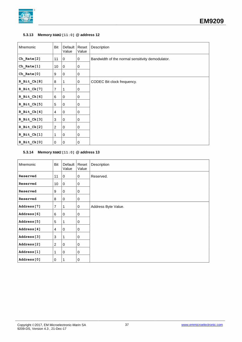
EM9209
Copyright 2017, EM Microelectronic-Marin SA 9209-DS, Version 4.3 , 21-Dec-17
37 www.emmicroelectronic.com
5.3.13 Memory RAM2[11:0] @ address 12
Mnemonic Bit Default Value
Reset Value
Description
Ch_Rate[2] 11 0 0 Bandwidth of the normal sensitivity demodulator.
Ch_Rate[1] 10 0 0
Ch_Rate[0] 9 0 0
R_Bit_Ck[8] 8 1 0 CODEC Bit clock frequency.
R_Bit_Ck[7] 7 1 0
R_Bit_Ck[6] 6 0 0
R_Bit_Ck[5] 5 0 0
R_Bit_Ck[4] 4 0 0
R_Bit_Ck[3] 3 0 0
R_Bit_Ck[2] 2 0 0
R_Bit_Ck[1] 1 0 0
R_Bit_Ck[0] 0 0 0
5.3.14 Memory RAM2[11:0] @ address 13
Mnemonic Bit Default Value
Reset Value
Description
Reserved 11 0 0 Reserved.
Reserved 10 0 0
Reserved 9 0 0
Reserved 8 0 0
Address[7] 7 1 0 Address Byte Value.
Address[6] 6 0 0
Address[5] 5 1 0
Address[4] 4 0 0
Address[3] 3 1 0
Address[2] 2 0 0
Address[1] 1 0 0
Address[0] 0 1 0

EM9209
Copyright 2017, EM Microelectronic-Marin SA 9209-DS, Version 4.3 , 21-Dec-17
38 www.emmicroelectronic.com
5.3.15 Memory RAM2[11:0] @ address 14
Mnemonic Bit Default Value
Reset Value
Description
Reserved 11 0 0 Reserved.
Reserved 10 0 0
Frequ[4] 9 0 0 Synthesizer’s RF Frequency LSB’s.
Frequ[3] 8 1 0
Frequ[2] 7 1 0
Frequ[1] 6 1 0
Frequ[0] 5 0 0
N_Pay[4] 4 0 0 Payload size of the Packet: N_Pay + 1
N_Pay[3] 3 0 0
N_Pay[2] 2 0 0
N_Pay[1] 1 1 0
N_Pay[0] 0 1 0
5.3.16 Memory RAM2[11:0] @ address 15
Mnemonic Bit Default Value
Reset Value
Description
Frequ[16] 11 0 0 Synthesizer’s RF Frequency MSB’s.
Frequ[15] 10 1 0
Frequ[14] 9 1 0
Frequ[13] 8 1 0
Frequ[12] 7 0 0
Frequ[11] 6 1 0
Frequ[10] 5 1 0
Frequ[9] 4 0 0
Frequ[8] 3 0 0
Frequ[7] 2 0 0
Frequ[6] 1 1 0
Frequ[5] 0 0 0

EM9209
Copyright 2017, EM Microelectronic-Marin SA 9209-DS, Version 4.3 , 21-Dec-17
39 www.emmicroelectronic.com
6. Packet information
The following details on the packet are provided for informational purposes only. Knowledge of the information contained here is not necessary for proper usage of the EM9209.
6.1 Packet format
In normal sensitivity mode, each packet contains the following information:
Preamble 3 * Address Byte Header Payload
Table 14: Packet format, normal sensitivity mode
Packet Information Length Description
Preamble =
5 * “11001100”
5 byte Clock recovery and data-slicer initialization.
3 * Address Byte 3 byte The preamble consists of 3 Address byte Address[7:0].
Header 0 or 1 byte
The 5 LSB’s of the header represent the payload size of the packet for communication subroutine available @ ROM_Boot_Address = 320.
For communication subroutine available @ ROM_Boot_Address = 192, header is
not existing.
Payload 0-32 bytes
Data
In high sensitivity mode, each packet contains the following information:
Marking Preamble 3 * Address Byte Header Payload
Table 15: Packet format, high sensitivity mode
Packet Information Length Description
Marking 14 ms Initial frequency step used to lock high sensitivity demodulator.
Preamble =
N * “11001100”
2 byte Clock recovery initialization.
3 * Address Byte 3 byte The preamble consists of 3 Address byte Address[7:0].
Header 0 or 1 byte
The 5 LSB’s of the header represent the payload size of the packet for communication subroutine available @ ROM_Boot_Address = 256.
For communication subroutine available @ ROM_Boot_Address = 128, header is
not existing.
Payload 0-32 bytes
Data
The size of the received packet including header and payload (stored in RXFIFO) can be read with the SPI command
Read_RXFIFO_Size(see Section 5.1.1.4). When RXFIFO has been completely read (until RXFIFO_Size[4..0] = 0) after
the previous reception, RXFIFO_Size[4..0] of the current packet is then the total packet size including the header.
The header byte is treated like a standard payload byte and must be stored in the TX_FIFO before the payload data prior to
transmit the packet in any mode.
For each byte, the most-significant bit (MSB) is sent first.

EM9209
Copyright 2017, EM Microelectronic-Marin SA 9209-DS, Version 4.3 , 21-Dec-17
40 www.emmicroelectronic.com
7. Versions and ordering information
The EM9209 is available in one Version as summarized in Table 16 below. The internal revision can be read in RAM1 (see
Section 5.1.1.6) at the address 63 after executing the SPI command ROM_Boot (see Section 5.1.1.16) with argument
ROM_Boot_Address = 0. Internal revision release format is xxyy, with xx = year (decimal) and yy = month (decimal).
Table 16: Version information
Version Description /Features Applications / Comments
1 Base 2.4GHz transceiver
- 26MHz crystal required
RF application when 1.9V to 3.6V Supply is available
Table 17: Ordering information
Ordering Code Description Packaging Container
EM9209V01WW7+ 1.5 to 72kbps Transceiver Wafer Wafer container
EM9209V01WS7+ 1.5 to 72kbps Transceiver Sawn wafer on tape
Wafer container
EM9209V01LF24B+ 1.5 to 72kbps Transceiver MLF24 Tape and Reel
8. Die Pinout
Figure 7: U9209 Die Pinout.
Die Size is 2000 x 1400 um.

EM9209
Copyright 2017, EM Microelectronic-Marin SA 9209-DS, Version 4.3 , 21-Dec-17
41 www.emmicroelectronic.com
9. Package information MLF24 4mm x 4mm
9.1 Package marking
1 2 3 4 5
A 9 2 0 9 0
B 0 1
C
A1-A4: Device type “9209” A5, B1-B2: Version “001” B3-B4: Week Number of Assembly (date of shipment from EM) B5: Blank C1-C4: Diffusion Lot Number (without year of diffusion & split) C5: Assembly House Code

EM9209
Copyright 2017, EM Microelectronic-Marin SA 9209-DS, Version 4.3 , 21-Dec-17
42 www.emmicroelectronic.com
10. Typical Applications
In this chapter, typical application scenarios for the EM9209 are described.
10.1 Application schematics
A typical application schematic for EM9209 is shown in Figure 8. The pins VBAT, VDD_SYNTH and VDD_RXTX are decoupled
with three 1uf capacitors (C1-C3). A 26MHz crystal (X1) is required for the RF and digital clock (crystal CL should be 10pF).
Finally a 200-Ohm PCB antenna (A1) can be used for the wireless link, or a 1:4 balun (50 : 200) can be used to interface to standard 50-Ohm antennas or test equipment.
.
VB
AT
200Ω loop antenna
C1
1μF
X1
C2
1μF
C3
1μF
3V
Battery
EM9209
VB
AT
AN
TN
AN
TP
DIV
_C
K
VS
S_
ISO
XO
UT
XIN
EN
_R
EG
SC
K
SS MO
SI
MIS
O
VS
S_
DIG
IRQ
VS
S_
RX
TX
VD
D_
RX
TX
VS
S_
RX
TX
VS
S_
DIG
Host Controller
VP
RO
G
TX
_O
N
RX
_O
N
VD
D_
SY
NT
H
VS
S_
SY
NT
H
Figure 8: Example application schematic of the EM9209
External component values, footprint, tolerance, and other requirements are shown in Table 18 for both of the example applications schematics.

EM9209
Copyright 2017, EM Microelectronic-Marin SA 9209-DS, Version 4.3 , 21-Dec-17
43 www.emmicroelectronic.com
Table 18: EM9209 application schematic external component details
Component Version Notes Value Footprint Description
A1 1 200 - Printed loop antenna
C1 1 1F 0402 VBAT decoupling capacitor, ±10%
C2 1 1F 0402 VDD_RXTX decoupling capacitor, ±10%
C3 1 1F 0402 VDD_SYNTH decoupling capacitor, ±10%
X1 1 1,2 26MHz - Crystal, ±20ppm, Example: TSS-3225J, CL=10pF
Note 1: Built in capacitors against ground are around 19 pF. 1 pf is left for bonding wire and PCB crystal pad.
Note 2: Crystal circuit tolerance calibrated after board soldering. Temperature dependence and aging shall not exceed ±20ppm.
EM Microelectronic-Marin SA (“EM”) makes no warranties for the use of EM products, other than those expressly contained in EM's applicable General Terms of Sale, located at http://www.emmicroelectronic.com. EM assumes no responsibility for any errors which may have crept into this document, reserves the right to change devices or specifications detailed herein at any time without notice, and does not make any commitment to update the information contained herein. No licenses to patents or other intellectual property rights of EM are granted in connection with the sale of EM products, neither expressly nor implicitly. In respect of the intended use of EM products by customer, customer is solely responsible for observing existing patents and other intellectual property rights of third parties and for obtaining, as the case may be, the necessary licenses. Important note: The use of EM products as components in medical devices and/or medical applications, including but not limited to, safety and life supporting systems, where malfunction of such EM products might result in damage to and/or injury or death of persons is expressly prohibited, as EM products are neither destined nor qualified for use as components in such medical devices and/or medical applications. The prohibited use of EM products in such medical devices and/or medical applications is exclusively at the risk of the customer