Embed Size (px)
Citation preview

EMBEDDED COMPONENTS ON THE WAY TO INDUSTRIALISATION
Hannes Stahr Mark Beesley
AT&S Leoben, Austria [email protected]
ABSTRACT Embedded component technology has been under visible development for the last twenty years, during which time significant progress has been made. Within the last three years, the Market demand for next generation miniaturization concepts has driven the industrialization of the embedded component concept, and today we see the first players manufacturing this technology in commercial production terms. This paper indicates the application areas for embedded component technology and the main field where the first applications are being launched to market. Module and chip packaging applications offer the most attractive benefits and the most interesting types of packages will be shown. An overview for the most interesting technologies that are used for chip embedding will roundup this section. Three years ago the European FP7 project HERMES (*) was started . Eleven partners from Industry and Research formed the consortium with the clear task to industrialize chip embedding technology. The requirements for the realization of chip embedding technology, the requirements for the equipment, the processes and the process environment is another topic of this paper. In the last chapter the technology roadmap will be shown driven by high end applications like smart phones and tablet PCs resulting in new packages for complex modules. But how are the business potentials? An outlook done by Yolé Development – doing market research in the field of packaging business – give a taste what is coming up in the future. (*) HERMES: High density integration by Embedding chips for Reduced size Modules and Electronic Systems. Key words: Embedding, chips, components INTRODUCTION The miniaturization trend in the semiconductor domain is predicted by Moore’s Law, with incredible development in the functionality of semiconductor devices. This constant growth of functionality combined with the
reduction of feature size (which is now in the range of 20nm) enables semiconductor devices with low power consumption at high operating speed. Dual core 1GHz processors for smart phones and other mobile applications are common today, typically having in the region of 900 I/O. These components are the technology drivers for smart phone PCBs – any-layer High Density Interconnect (HDI) constructions with stacked copper filled via are needed to fan out these complex components. The any-layer interconnection concept is the optimum that can be achieved in a PCB for high density interconnections. The options for the future are the further reduction of feature size and the layer increase of the multilayer. Component embedding opens the door to new opportunities in the miniaturization of devices. The foot print of a device and the thickness can be reduced in one step. APPLICATION FIELDS FOR EMBEDDING TECHNOLOGY PCB and module applicationThe cost and the performance of a product are major determining parameters relating to its success potential in the Market. The cost of components and yield of the product are once again major cost drivers. Taking these facts in mind one can start to determine the application fields where the embedded component concept can be successfully applie.
The first application for embedded components are multilayer PCB and / or HDI PCB with embedded passives – resistors, capacitors, ESD protection devices and simple ICs or semiconductors. The value of the components is in a similar range to the PCB and with a production yield above 95% this product becomes competitive and significant existing production capabilities can be used. One comment that must be made though is that build-ups with integrated semiconductors, ESD compliance is a must. For this requirement the PCB world is not prepared according to our experience, and much more specific protocols must be implemented.
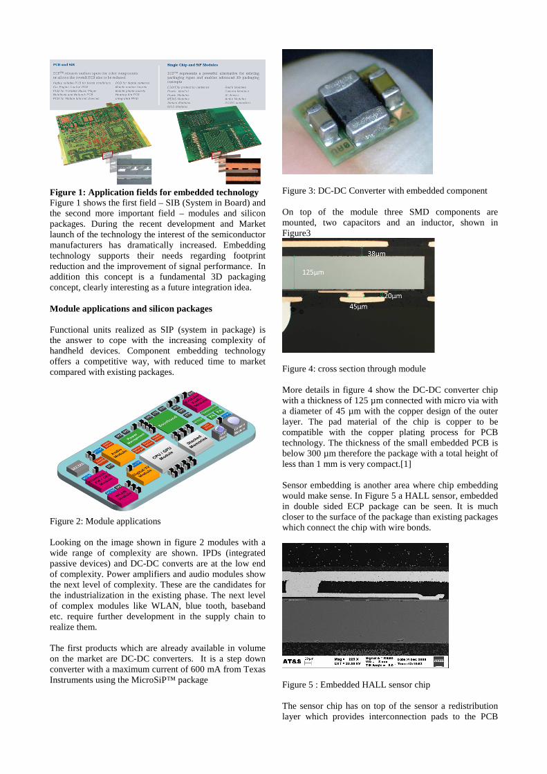
Figure 1: Application fields for embedded technology Figure 1 shows the first field – SIB (System in Board) and the second more important field – modules and silicon packages. During the recent development and Market launch of the technology the interest of the semiconductor manufacturers has dramatically increased. Embedding technology supports their needs regarding footprint reduction and the improvement of signal performance. In addition this concept is a fundamental 3D packaging concept, clearly interesting as a future integration idea. Module applications and silicon packages Functional units realized as SIP (system in package) is the answer to cope with the increasing complexity of handheld devices. Component embedding technology offers a competitive way, with reduced time to market compared with existing packages.
Figure 2: Module applications Looking on the image shown in figure 2 modules with a wide range of complexity are shown. IPDs (integrated passive devices) and DC-DC converts are at the low end of complexity. Power amplifiers and audio modules show the next level of complexity. These are the candidates for the industrialization in the existing phase. The next level of complex modules like WLAN, blue tooth, baseband etc. require further development in the supply chain to realize them. The first products which are already available in volume on the market are DC-DC converters. It is a step down converter with a maximum current of 600 mA from Texas Instruments using the MicroSiP™ package
Figure 3: DC-DC Converter with embedded component On top of the module three SMD components are mounted, two capacitors and an inductor, shown in Figure3
Figure 4: cross section through module More details in figure 4 show the DC-DC converter chip with a thickness of 125 µm connected with micro via with a diameter of 45 µm with the copper design of the outer layer. The pad material of the chip is copper to be compatible with the copper plating process for PCB technology. The thickness of the small embedded PCB is below 300 µm therefore the package with a total height of less than 1 mm is very compact.[1] Sensor embedding is another area where chip embedding would make sense. In Figure 5 a HALL sensor, embedded in double sided ECP package can be seen. It is much closer to the surface of the package than existing packages which connect the chip with wire bonds.
Figure 5 : Embedded HALL sensor chip The sensor chip has on top of the sensor a redistribution layer which provides interconnection pads to the PCB

micro via. With the reduction of the distance between the sensor and the magnetic actuator the sensitivity could be increased by factor 10. THE HERMES CONSORTIUM AND THE TASK OF THE PROJECT Developments of chip embedding technology in European consortia started in 2000. The main working fields at this time revolved around the selection of base materials and the development of interconnect technologies to the chip. On the back of rising interest in chip embedding concepts, the Hermes consortium was founded in 2008 to run an industrialization project for chip embedding. This project is approaching the successful end of a three year funded period, from the European Commission in the FP7 framework. The consortium is organized in a supply chain as shown in figure 6. The end users come from the
Figure 6: Structure of the consortium automotive, industrial and security areas. The requirements on reliability for the chip embedding technology vary. The applications range from a motor control module to a power module for an industrial application to a security communication device. The consortium covers all aspects of product realization, from wafer supply, backend processing of the wafers, embedded PCB design and test to prepare the chip for the embedding process. Around the embedding process material and process suppliers are on board to enable the development of the required process technology. To achieve the design requirements for ultrafine line technology a modified semi-additive process is used. Circuit Foil has developed an ultra-thin copper foil and Atotech supported the semi-additive plating process with newly developed plating equipment (Single Board Processor or SBP). For the embedding process of discrete components the assembly process is supported by an existing machine platform from originally Siemens, and now ASM. The scientific partners enable the development of the technology for the next generation of embedding applications for component pitches of 100 µm and below. The development of 15µm fan out technology is the target for the scientific partners. The industrialization target for the Hermes consortium is to achieve volume production with 25µm fan out technology with a component pitch of 175 µm (peripheral pitch) or 225 µm pitch with one line per channel. Beside the Hermes consortium a group of companies support the project. Wafer back end support is given by Flip Chip International. They have developed their
processes to be compliant with the embedding processes and they supplied redistribution layers on the dies for embedding. FCI supported Hermes in addition with chip thinning, chip dicing and tape on reel services One of the big topics was the generation of the board design for embedded applications. The existing EDA (Engineering Design Automation) design tools don’t support the requirements for discrete embedded components. Work-around have been used to make the first designs with the risk of not having design rule checks available. Confronted with this situation the consortium contacted the most important EDA tool suppliers and convinced them to support Hermes. This consists of the following EDA tool suppliers: Cadence, Mentor Graphics, Pulsonix and Zuken. The first activity was the evaluation of the capabilities of the tools and the generation of a gap list as shown in figure 7. Since the start of this collaborative work two of the supporters released their EDA tools and closed nearly all gaps which have been identified. One of these releases were used to design the most complex functional demonstrators – the security demonstrator - in the Hermes project.
ECP® component placement between copper layers
ECP® component pads available for via interconnect
ECP® component with pads on top and bottom side
Possibility to flip and/or rotate each ECP® component separately
Component span over several copper layers
Additional layers for ECP® - assembly, glue spots, cavities
Separate assembly output for ECP® components
ODB++ support for ECP®
Gerber/Excellon support for ECP®
Via-in-pad technology
Filled/stacked via support for sequential buildup
Figure 7: gap list for EDA tools THE ECP TECHNOLOGY Embedded Components Packaging, ECP, technology is a laminate-based chip embedding technology leveraging the core principles of PCB manufacturing. It is a combination of state of the art HDI micro via technology, ultra-fine line technology based on a modified semi- additive technology and a component assembly technology adapted for discrete passive components for embedding and modified active components. The technology for chip embedding is a chip first technology – the chip is embedded first in a PCB creating an embedded core. This embedded core can be built in to

a multilayer board or HDI build up layers are used to provide enhanced routing density. The embedded core itself is already a package for the silicon chip. This option is used today for the first embedded applications. For comparison when using chip last technology the board is built first and then the chip is placed in a cavity and connected with the board e.g. by soldering and afterwards the board is finished – Figure 8 shows the principle of the technology
Figure 8: Chip last technology When using chip last technology the prefabricated board can be tested and only good boards will be assembled with components. This advantage is useful when high cost components are embedded. The combination of chip first and chip last technology is a quite interesting one when complex modules should be realized. Especially the assembling components in cavities offer a reduction of the height of the module. With new technologies like 2,5DC® cavity formation becomes cost effective shown in figure 9. The 2.5DC® technology uses only standard materials and processes for HDI technology.
Figure 9 : cavities with 2.5DC technology The left picture in figure 9 shows a cavity where a chip will be assembled and wire bonded. The right picture shows an example of a Chip Scale Package (CSP) component assembled in a cavity. The chip last technology can be mainly found in Asia. The different versions of chip last technology are summarized in the Standard on Device Embedded Substrate - Terminology / Reliability /Design Guide JPCA-EB01[2] The principle process flow of the chip first technology is shown in figure 10. The process starts with a laser marking process to define registration marks for mechanical process steps. On the copper foil an adhesive material is printed and in the next step the discrete components are placed in the adhesive. This adhesive will
be cured to get a solid bonding to the copper foil so that no movement of the component can occur in the next process steps. In the lamination process the copper foil with the mounted components, FR-4 prepregs with openings in the component area, a prepreg without openings and a further copper foil are registered together. This package is laminated in a multilayer press to create the embedded core. Drilling of laser via to the copper pads of the components and drilling of through holes in the ECP® core are the next process steps that are very similar to HDI technology. Following via formation is hole cleaning and electro-less copper plating of the holes. After electro-less copper plating we enter the modified semi-additive process: A high resolution photoresist is laminated on the ultra-thin copper foil followed by the imaging process of the resist. The resist is developed and in the non-covered areas of the resist the copper pattern is built up by galvanic plating. The remaining photo resist is then stripped away and the ultra-thin copper foil that is exposed after the resist stripping is removed by flash etching.
Figure10: process flow for an ECP® core The processing of the ECP® core ends with an automatic optical inspection to detect failures and deviation of the copper pattern. More complex modules can be built by adding buildup layers to the ECP® core. This is done by multiple laminations of thin FR-4 prepregs laser drilling and copper filling of the micro via to enable via stacking. Via stacking is a must for realizing these complex packages to route 2 – 5 lines per component pitch. Galvanic via filling in combination with ultra-fine line technology is quite challenging and requires new plating concepts and plating equipment. Requirements for the ECP production line Production yield gets a new significance when you consider a product utilizing ECP technology. Even 1% yield loss has a big impact on the total cost of a product when you take in mind that the silicon chip that is embedded can cost up to ten times more than the laminate package. The processes that are selected have to fulfill requirements above HDI PCB processes from the view of stability and repeatability, and the human factor plays an important role beside the manufacturing processes. The

handling of embedded products is a potential source of failures and it has to be optimized from “the bottom up”. The handling in the machines and the handling from machine to machine needs a new setup. To get the right mind-set for this task it makes sense to look into the production where the high value product is made and learn their lessons. Let’s consider the set up for silicon dies production – a silicon fab. There you can learn a lot about handling, tracing of products and a bullet proof system to eliminate human errors. Of course this system costs a lot of money but it stands in a ratio with the high value of the wafer that is produced. For an embedded production line there exist similar rules and we have already implemented parts of them. In the embedding production line large panel formats with a typical PCB panel format of 18”x24” are processed. Large format processing enables cost efficient production and requires special equipment. Compared with the typical panel format for packaging substrates the production format for embedding is 18 times larger. The embedding process starts on a special copper foil which was developed in the frame of the Hermes project it is a 2µm copper foil on a copper carrier with very low treatment roughness as shown in figure 11 [3]
Figure 11: 2 µm copper foil on 70 µm carrier This copper foil combines good foil handling during the embedding process and a protection of the sensitive surface of the 2 µm copper foil. Low copper treatment of Rz = 1,8 µm and a thin resin layer on top guarantee high copper bonding force even to high Tg materials. On this copper foil an adhesive is printed which forms the isolation layer between the component and the copper foil. The control of the volume of the adhesive is important as it defines the dielectric thickness. Process control with large area scanners enables fast measurement of the adhesive thickness after printing. This machine is a must for process development and production control. The component assembly process is done with an accurate assembly machine for SMD assembly. The machine from ASM has two assembly heads a twin head for high
precision and a 20 nozzle head for high through put assembly. The twin head is mainly used for large die assembly as seen in Figure 12
Figure 12: high precision die assembly The requirements for the camera and registration system is different to standard assembly because the visible surface is either copper and silicon passivation, or ceramic and copper for passive components. Table 1 shows the specified and the measured accuracy of the X2 assembly machine.
Table 1: accuracy data of assembly machine
Figure 13 shows a daisy chain component of a Hermes test vehicle. It has a dimension of 7,5 x 7,5 mm with pad sizes of 150 µm. In this case registration to the contour of the chip is not good enough to achieve the requested accuracy. The vision system needs to register to the copper pads on the chip therefore high resolution cameras are needed.
Figure 13: daisy chain chip In Figure 14 a more complex module after assembly can be seen. It is a two chip module – each 5 x 5 mm chip has 150 interconnects and about 100 passive components mainly capacitors. [4]
20 Nozzle head Twin head Max. speed 20000 comp/h 3700 comp/h Accuracy specified +/- 55 µm, +/- 0,7° +/- 30 µm, +/- 0,07° Accuracy measured +/- 20 µm, +/- 0,035° +/- 11 µm, +/- 0,025°

Figure 14: module after assembly After the lamination process, the embedded core is finished. The core is then processed through laser drilling for via formation and these holes are cleaned and plated with electro-less copper. Then the sequence for the ultra-fine line semi-additive process starts. Digital imaging of the photo resist is critical process for 25µm technology and below. This is done with a LDI system that is capable to image down to 10 µm line and space. This machine addresses 25000 DPI or 1 µm data resolution with the capability to adjust the image to registration marks with a maximum failure of 18 µm. The capability to adjust the image on the fly is a very important feature to compensate dimensional instability of the PCB materials. Digital imaging offers more important features to make the product traceable. Individual tracing data can be imaged to every customer panel or card. For the handling of a product with 25µm technology and smaller no compromises are allowed. A touch-less transport for the panels is needed. At least the image area needs to fulfill this requirement. This transport concept is shown in figure 15 – the production panel is fixed in a frame which is transported through the machine.
Figure 15: touch less handling All critical process steps in the semi-additive process sequence have to use touch-less handling. The machines use new technology for the wet chemistry separation which is normally done by rollers. After development of the photo resist with an alkaline solution, the boards are plated in unique plating equipment – the single board processor. Every panel is
plated in a single panel plating bath. This enables full process control where all important plating bath parameters are controlled online and the process data are stored with the identification number of the panel. Best plating uniformity has highest priority therefore the single board processor has a cathode frame that contacts the panel on all edges. Segmented, individually adjustable anodes ensure world class plating uniformity. In addition a new flood delivery system enables low plating tolerances even with filled via and ultra-fine line technology. Figure 16 shows a top view in the plating cell. In the middle parts of the cathode frames are visible.
Figure 16 : Plating cell of an industrial single board processor The single board processor is designed to fulfill best in class plating requirements. It was tested with patterned design down to 9 µm line and space. The SBP with its excellent flow and filter system enters new application fields – wafer plating and TSV plating. Traceability of materials for the PCB production and embedded components needs to be fully available. The PCB world is not prepared for this depth of traceability. On one side the logistic capabilities need to be adapted and upgraded on the other side the process equipment needs the capability to identify the product and mark the product with individual data. The tracing depth for the embedded silicon is on wafer level. The future requirements end on chip level. That means every final module traces back to the chip position on a wafer in a wafer batch. Tracing of process data back to the individual production panel is another topic which is requested. Single panel production supports this request in a very good way – with individual panel identification and the mapping of the process data to the panel it can be realized. Beside clean room environment which is installed in all production areas ESD control is required. ESD control of the production environment is a must when handling electrostatic sensitive devices. For a PCB fabricator this requirement is nearly unknown. One of the challenges to build the ECP® production line was the specification of ESD compliant equipment which is manufactured form suppliers for PCB production machines. Even the

selection of ESD compliant materials and the adaption of processes was some hard work. The ECP® production line is approved also by customer audits according ESD compliance. THE ECP ROAD MAP AND THE BUSINESS Embedded component technology became visible with prototypes and small series in the last 10 years. Since one year the first volume products are ramping up. Some companies worldwide have started volume production with different technologies depending on the product requirements and complexity.
Figure 17: ECP® technology roadmap 3D packaging is the topic that is already requested and realized when looking at figure 18 – it shows a memory stack. The dies are connected via silicon via. [5]
Figure 18: memory stack connected with TSV For embedded application this extreme interconnection density cannot be achieved in the next future. The ECP package offers another possibility of component stacking. On top of the module dies, CSPs and passive components can be assembled. Today passive components will be assembled but in the near future the first modules with silicon components will follow – as shown in figure 17. This option will enable the realization of more complex modules. In Hermes one of these complex modules has been developed which is shown for 2013. It is a motor management module with a size of 13 x 13 mm with an embedded processor die with a size of 8,5 x 8,5 mm. on top of the ECP package the memory and other active and passive components are mounted. Figure 19 shows some details of this module.
Figure 19: Motor management module The ECP module is a 6 layer board construction with the ECP core and two buildup layers, stacked via interconnection and 25µm technology in all layers as shown in the top picture of figure 19 are needed. Up to 4 lines per channel are routed though via pads of the 350 µm pitch embedded component. The picture below shows more details of the cross section. The processor has on the top side a redistribution layer, and it is connected with copper filled via to the outer layer of the ECP core. Beside the technical requirements of the realization of this product the functional testing of complex modules is a challenge for the complete supply chain that has to be managed. Today only some basic functional tests can be done which are by far not enough to go to production. With this demonstrator developed in the Hermes project it becomes visible that the development of the supply chain and an appropriate business model has high priority. Yolé Development is one of the leading market research companies for semiconductor packaging market. They have analyzed the requirements for new packaging applications. In figure 20 they see two main streams for embedded packages: The fan out wafer level packages and the embedded die PCB substrates. Fan out wafer level packages are driven by die shrinkage and the increasing number of I/O. All necessary interconnection points have to be placed on a 400 µm grid today and on a 300 µm grid maybe in some years. One solution to deal with this situation is the fan out package. The eWLP technology was developed by Infineon using silicon backend equipment to manufacture the fan out layer on a molded package. ASE and STATS Chip PAC has taken license from Infineon and doing production of this package.

Figure 20: Outlook for embedded wafer level packages [6] Embedded die technology is the competing technology using PCB technology and processes. Yolé see both technologies to take a major role for packaging for the next generation like system in package and package on package. They see that both technologies have started recently in 2010 with products on the market. CONCLUSION: A long development phase for embedded component technology is coming to an end and the first volume products are available. New small packages with embedded chips are enabling further miniaturization for hand held high end devices. Smart phones seem to be the enablers for the next generation of more complex modules. Beside more demanding technologies supply chain management and the issue of cost optimized functional testing are the challenges which have to be handled. Hermes an FP7 project with a consortium of eleven partners was started three years ago with the clear target for the industrialization of the chip embedding technology. A funded project with an industrialization target is a novelty for the European Commission. Hermes acts as a spearhead for the implementation of the chip embedding technology. Exploitation of the project results have already been done resulting in volume production of chip embedded modules. High end chip embedded modules for the next generation of technology has been developed to support the future Business. The production capabilities needed for a chip embedding production line are definitely above a PCB HDI production line. A dedicated ECP production line for high volume production has been installed using new machine concepts for processing and handling high value products. Discrete component assemblies of passive components and silicon dies, digital imaging, a modified semi-additive process 25 µm line/space capable are the high lights of the ECP production line. High yield production and full traceability down to the wafer is realized to fulfill the requirements for chip embedding business.
References : [1]: Product analysis Fraunhofer IZM of DC-DC converter [2]: Standard on Device Embedded Substrate - Terminology / Reliability /Design Guide JPCA-EB01 [3]: Circuit foil data sheet of DTH-TZA-PA [4]: H.Stahr et al. : Development of a Design & Manufacturing Environment for Reliable and Cost-Effective PCB Embedding Technology, ", Proceedings of IPC APEX Conference, Las Vegas, USA, April 2011. [5]:http://www.amkor.com/index.cfm?objectid=7478706F-E1C7-1A4D-E62795E72380FA68 [6]: Market report: Yolé Development