Embed Size (px)
Citation preview

The Pennsylvania State University
The Graduate School
College of Engineering
EMBEDDING ELECTROMAGNETIC COMPONENTS INTO CUBESAT
STRUCTURES USING ADDITIVE MANUFACTURING
A Thesis in
Electrical Engineering
by
Rebecca A. Arenson
© 2017 Rebecca A. Arenson
Submitted in Partial Fulfillment of the Requirements
for the Degree of
Master of Science
December 2017

ii
The thesis of Rebecca A. Arenson was reviewed and approved* by the following: Sven G. Bilén Professor of Engineering Design, Electrical Engineering, and Aerospace Engineering Thesis Advisor Timothy J. Kane Professor of Electrical Engineering and Meteorology Nicholas A. Meisel Assistant Professor of Engineering Design Kultegin Aydin Professor of Electrical Engineering and Department Head * Signatures are on file in the Graduate School.

iii ABSTRACT
Grant funding and National Aeronautics and Space Administration launch initiatives for
CubeSats make research using satellites research available to universities and projects with
relatively low budgets. The small scale of CubeSats—only 10 cm × 10 cm × 10 cm per 1U (one
unit) cube—requires efficient use of spacecraft volume. Many CubeSats employ measuring-tape
dipole antennas that provide only low directionality, or patch antennas that take away surface
area needed for solar panels. Additive manufacturing has also become an important topic of
research as 3-dimensional printing techniques improve. This work explores techniques for using
additive manufacturing to save space on small satellites by embedding electromagnetic
components, such as antennas, into the structural elements of a CubeSat. Two primary methods
are analyzed, one using finite deposition modeling printing and one using stereolithography.
These two types of printers were selected because they are easily accessible and affordable. The
filaments for the finite deposition modeling method proved insufficient for this application at this
time. However, the stereolithography method successfully produced conductive components
embedded within structural elements, including an antenna embedded in a CubeSat cross-brace.

iv TABLE OF CONTENTS
LIST OF FIGURES ..................................................................................................... v
LIST OF TABLES ....................................................................................................... vi
ACKNOWLEDGMENTS ........................................................................................... vii
Chapter 1 Introduction ................................................................................................. 1
Motivation ........................................................................................................................ 1 Multifunctional Materials................................................................................................. 3 Cost Constraints ............................................................................................................... 4 Contributions of Thesis .................................................................................................... 4 Overview of Thesis .......................................................................................................... 5
Chapter 2 Background on 3D Printing of Antennas .................................................... 6
3D Printing for Optimal Geometry .................................................................................. 6 3D Printing Dielectrics to Increase Gain.......................................................................... 7 Embedding Antennas into Structures ............................................................................... 8
Chapter 3 Methods for Embedding Conductive Elements into Additively Manufactured Parts ...................................................................................................................... 10
Carbon Fibers ................................................................................................................... 11 Metal-Infused Filaments .................................................................................................. 11 Printing Metallic Ink on FDM Parts ................................................................................. 12 Injecting Conductive Material .......................................................................................... 13
Chapter 4 Experimental Results................................................................................... 14
Method ............................................................................................................................. 14 Design Considerations ..................................................................................................... 16 Vacuum Testing ............................................................................................................... 16 Conductivity ..................................................................................................................... 19 Relative Permittivity ........................................................................................................ 21 Dipole ............................................................................................................................... 23
Chapter 5 Conclusions and Future Work ..................................................................... 29
Summary .......................................................................................................................... 29 Potential Applications ...................................................................................................... 29 Future Work ..................................................................................................................... 30
BIBLIOGRAPHY ........................................................................................................ 31

v LIST OF FIGURES
Figure 1: Generic CubeSat dimensions .................................................................................... 2
Figure 2: Generic CubeSat configuration ................................................................................ 3
Figure 3: Conformal antenna during the printing process [4] .................................................. 7
Figure 4: Three Dielectric Reflectarray Prototypes [6] ............................................................ 8
Figure 5: Methods for embedding antennas. (a) Pressed between two substrates [8] and (b) replacing struts with antennas on printed circuit boards [9] ............................................ 9
Figure 6: Melted Virtual Foundry filament in oven ................................................................. 12
Figure 7: Embedding conductive pathways into an SLA part ................................................. 15
Figure 8: Test blocks in the vacuum chamber ......................................................................... 18
Figure 9: Resin leakage after vacuum testing .......................................................................... 19
Figure 10: Conductivity test setup ........................................................................................... 20
Figure 11: Conductivity test block. Hole diameter from top to bottom: 0.5 mm (closed off with resin), 1 mm, 2 mm, and 4 mm. ....................................................................................... 20
Figure 12: Test block filled with NuSil conductive adhesive .................................................. 21
Figure 13: Microstrip line (Front View) .................................................................................. 22
Figure 14: Microstrip line (Back View) ................................................................................... 22
Figure 15: S11 of the microstrip line ......................................................................................... 23
Figure 16: Dipole embedded in resin ....................................................................................... 24
Figure 17: S11 of dipole antenna............................................................................................... 24
Figure 18: Dipole attached to CubeSat frame as cross-brace .................................................. 25
Figure 19: S11 of dipole in CubeSat frame ............................................................................... 26
Figure 20: Dipole with ground plane in CubeSat frame .......................................................... 27
Figure 21: S11 of dipole with ground plane in CubeSat frame ................................................. 28

vi LIST OF TABLES
Table 1: Mass before and after vacuum ................................................................................... 17
Table 2: Resistance over 5 cm ................................................................................................. 20

vii ACKNOWLEDGMNTS
I would first like to thank FormLabs for printing all the SLA parts and Swapnil Sinha for
printing all the FDM parts used in this thesis. I would also like to thank my advisor Dr. Sven
Bilén for his assistance and patience and Dr. Kane and Dr. Meisel for serving on my committee.
I have also been helped and by my labmates in SSPL and would like to thank Sergio Gallucci
and Thomas White for their support, as well as the OSIRIS-3U CubeSat we built together and
that provided inspiration for this work.

1
Chapter 1
Introduction
Satellites and additive manufacturing are two exciting technologies that are emerging into
broader markets and becoming more affordable. Two of the elements that require a large amount
of resources (e.g., size and mass) on any satellite are its structure and antennas. This work
presents a method for combining these components using low-cost additive-manufacturing (AM)
techniques.
Motivation
CubeSat size is defined in increments of “U”. 1U is 10 cm × 10 cm × 10 cm (1000 cm3)
in volume and typically allotted approximately 1.33 kg in mass. A typical CubeSat for a
university research mission may be 1U, 2U, 3U, or 6U, for a maximum volume of 6000 cm3.
Figure 1 shows standard CubeSat dimensions and Figure 2 shows a generic 1U configuration.
Many of the components are becoming increasingly smaller and more powerful to address the
increased volume, power, and computational requirements of the satellite’s payload. However,
most CubeSats still rely on fairly rudimentary measuring-tape dipoles/monopoles [1] or patch
antennas. These solutions typically are either low-gain or require large amounts of satellite
surface area, which takes away from area that can be allotted to solar panels.

2
Figure 1: Generic CubeSat dimensions
Some universities have already experimented with 3D printing their structures using
metal printers. However, these experiments have accomplished little more than to replace
traditional manufacturing techniques. The European Space Agency (ESA) has begun
experimenting with 3D printing plastic CubeSat bodies using special filaments [2]. However,
the work described in this thesis uses AM to turn the CubeSat structural elements into
multifunctional components that include other elements such as antennas.
By incorporating antennas into the structural components of the satellite, it is possible to
implement antenna geometries and arrays of antennas that otherwise would be difficult to
accommodate within the small confines of a CubeSat. For example, antennas could utilize
multiple faces of the satellite. Coaxial cabling could run through the side rails instead of filling
interior space. Arrays of antennas could line the perimeter of the structure without reducing the
area allocated to solar panels. This technology may allow additional research that is currently
constrained by limited surface area or volume.
10 cm 10 cm
10 cm
10 cm 10 cm
20 cm 10 cm
100 cm 100 cm
1U 3U 6U

3
Figure 2: Generic CubeSat configuration
Multifunctional Materials
The term “multifunctional material” refers to the use of one component to serve two or
more purposes. These materials are particularly useful for space and mass-constrained
environments, by allowing more efficient use of the area, volume, and mass budgets. Siha [3]
discusses methods for embedding electrical components into materials while maintaining the
strength of the part, demonstrating one form of a multifunctional material. In this thesis, two
specific functions are addressed: structural support for a small satellite and electromagnetic
applications. In order to fulfill both requirements, the material must contain a dielectric and a
conductive component. The conductive component serves as, for example, a radiating element
and must have low enough resistivity so as to not cause produce noticeable loss across the scale
lengths of a CubeSat (10s of cm). The dielectric material is necessary to isolate individual
conductive elements, act as substrate, and provide structural integrity. These two aspects of the
multifunctional material must also be able to withstand the space and launch environment while
maintaining cohesion between the dissimilar materials.
Structure Power
Command & Data Handling
Guidance Navigation & Control
Communications
Solar Panels Antenna

4 Cost Constraints
While CubeSats, on occasion, can have large budgets, typically they do not. Many are
funded by grants and donations, and designed and built by student (i.e., volunteer) labor.
Although there are many expensive AM technologies, these were not considered due to their cost
and limited availability. Instead, this thesis focuses on desktop 3D printers and inexpensive
materials. Finite Deposition Modeling (FDM) printers, such as the Markforged and Makerbot,
are already commonplace in universities and industry. FormLabs has now made
stereolithography (SLA) printers, the Form1 and Form2, nearly as affordable and with higher
print quality. These printers are so affordable, they could potentially reduce the cost of
manufacturing a structure while leveraging the benefits of rapid prototyping, which is ideal in a
research environment.
Contributions of Thesis
This thesis presents a proof-of-concept method for embedding antennas and other RF
components into small satellite structures. This method could be used as a low-cost solution to
save volume and allow additional research instruments to be included on CubeSats. The method
was demonstrated by performing material properties tests on components manufactured using the
method and constructing an antenna embedded into a cross-brace sized SLA-printed part.

5 Overview of Thesis
This thesis first presents a background on 3D printing of antennas in Chapter 2, including
the ability to optimize the geometry of the antenna and dielectric into otherwise-difficult-to-
manufacture shapes. It also discusses previous methods for embedding antennas into structures.
Chapter 3 explores the use of different methods and techniques to meet the research goals and
evaluates each option against the research criteria. Chapter 4 presents a successful method using
an SLA printer and conductive paint, as well as the experimental data collected on this method
that demonstrates its feasibility. Chapter 5 summarizes the findings, suggests future work, and
concludes this thesis.

6
Chapter 2
Background on 3D Printing of Antennas
Additive manufacturing can be used in multiple ways to improve antenna design and
manufacturability. This chapter provides a literature review of ways in which 3D printing can
improve the geometry of antennas and dielectrics, as well as the embedding antennas into
structures.
3D Printing for Optimal Geometry
3D printing opens up new options for antenna geometries that were not possible with
traditional manufacturing techniques. One traditional method is to produce flat antennas on
printed circuit boards (PCBs). 3D printers using silver or copper nanoparticles can extend that
method onto three-dimensional substrates. Adams et al. [4] present a method for creating
electrically small antennas by conformal printing with metal ink on convex or concave dielectric
surfaces, as shown in Figure 3. This technique could be useful for CubeSats that use amateur
radio bands in the Ultra High Frequency (UHF) range, where the wavelength is large compared
to the spacecraft size. The potential to adapt this method with different substrates is discussed in
Chapter 3.

7
Figure 3: Conformal antenna during the printing process [4]
Other researchers use printers that sinter metal to produce unique shapes. Lopez and
Lopez [5] were able to add complexity and better optimize an ultra-wideband antenna using 3D
printing. Often, AM can reduce the assembly time required for complex antennas or reduce the
need for custom machinery. This is particularly useful for one-off antennas and rapid
prototyping. However, these metal printers are typically extremely expensive both to purchase
and to operate and do not provide opportunities to incorporate dielectric materials. While it may
be possible to print a fully metal part that can act as both a structural element and an effective
antenna, there must be some dielectric in place to isolate the antenna from spacecraft ground.
3D Printing Dielectrics to Increase Gain
In addition to the printing of metal antennas, it is also possible to use plastic-extruding
3D printers to create dielectrics in unique shapes for use as substrates or lenses. Nayeri et al. [6]
present a low-cost solution for increasing antenna gain by varying the height of the dielectric
elements within their reflectarray designs shown in Figure 4. 3D printing allows for detailed
customization that allows for greater optimization of these dielectric components. Similarly,

8 Bisognin et al. [7] achieved a 10-dB improvement in a 60-GHz antenna solution by 3D printing a
lens. These two papers show that, when properly optimized, 3D-printed plastics overtop an
antenna can improve performance. It can be inferred that similar techniques used to print
optimized substrates with unique geometries may also improve performance. Some methods for
embedding antennas described in Chapters 3 and 4 require dielectric material surrounding the
radiating element. While it is important to avoid highly lossy materials that would degrade the
signal, the shape of the dielectric can be utilized to shape the antenna pattern.
Figure 4: Three Dielectric Reflectarray Prototypes [6]
Embedding Antennas into Structures
This thesis presents methods for embedding antennas specifically into CubeSat
structures; however, the idea of embedding antennas into other materials has been applied to
other applications. For example, in 1965, Boicey [8] patented a system for embedding an
antenna in a car window by sealing the antenna between two glass sheets. With modern 3D-
printing techniques, a similar outcome could be achieved by using the method described by
Adams et al. [4]. However, this shows that embedding antennas into other objects has existed as
an application for nearly as long as antennas themselves.

9 Today, vehicles rely heavily on wireless communications. Just like satellites, aerial
vehicles also face tight size and weight constraints. Sharawi, Aloi, and Rawashdeh [9] embeded
an array of antennas into an unmanned aerial vehicle (UAV) by using printed antennas as the
wing struts. The success of embedding antennas into UAVs shows the promise for finding a
similar technique to work on small satellites. This thesis attempts to use the advantages of the
AM techniques described earlier in this chapter to improve on these methods for embedding
antennas, shown in Figure 6.
Figure 5: Methods for embedding antennas. (a) Pressed between two substrates [8] and (b) replacing struts with antennas on printed circuit boards [9]
(a) (b)
Ant
enna
Gla
ss
Gla
ss
Antenna Array
10
Chapter 3
Methods for Embedding Conductive Elements into Additively Manufactured Parts
Three-dimensional printing techniques can be classified by the type of material and the
process used to create parts. Many metal printers require extremely high temperatures to sinter
metal powder. These temperatures would melt or evaporate any plastic-based dielectrics. These
techniques were excluded based on their inability to perform as a multifunctional
electromagnetic component. However, they are often used to create structures that include heat
sinks, reflectors, and other functions. The most common type of non-sintering metal printer is a
metallic ink-jet printer, which is explored later in this chapter.
Plastic-based AM techniques generally employ either a powder, resin, or filament.
Typical processes include sintering, laser curing, or extruding. Both 3D printing companies and
research institutes are currently working to improve the speed, accuracy, layer thickness, and
material properties of these printers. This thesis focuses on desktop printers that are accessible
and affordable for low-budget projects. The two most common desktop techniques are Finite
Deposition Modeling (FDM) and Stereolithography (SLA).
FDM printers extrude a filament into a three-dimensional part. This technology is
becoming increasingly common and cost effective. Standard materials include Acrylonitrile
Butadiene Styrene (ABS) and Polylactic Acid (PLA) plastics. These plastics can also be
combined with other materials, such as carbon fiber or metal, to create filaments with a variety of
properties. It is also possible on some printers, or by modifying desktop FDM machines, to print
space-rated dielectrics such as Ultem [10].

11 Stereolithography (SLA) uses a laser to cure layers of resin. SLA printers typically have
finer detail and thinner layers than FDM machines. While many types of resins already exist to
work with existing printers, it is also possible to mix resins to create unique properties. These
special resins can have specific dielectric and mechanical properties.
Carbon Fibers
Some printers, such as the Markforged FDM printer, can lay down carbon fiber while
printing nylon filament. The nylon acts as a dielectric, while the carbon fiber acts as a
conductor. As such, it is possible to print conductive components that are fully enclosed in nylon
that could be used as antennas. However, the high resistivity of the carbon fiber causes large
losses and nylon is unsuitable for space applications [11]. It may be possible to use a fiberglass
material instead of nylon and enhance the conductivity of the carbon fiber through silver coating
in order to adapt this technology for space applications.
Metal-Infused Filaments
Several desktop FDM printers have dual nozzles that allow them to print multiple
filaments on the same part. The majority of filaments contain ABS or PLA plastic. Many
experimental materials infuse the filament with metallic particles or fibers. Despite including
metal particles, current filaments are non-conductive or highly resistive at best. Virtual Foundry
claims to make a filament that, once cured in a kiln, is nearly 100% metal [12]. However,
experimental tests showed that the material remained non-conductive after an hour at 100 °C and
melted above 160 °C, as shown in Figure 7. It is only possible to achieve conductivity by

12 sintering the part, which would melt or evaporate any dielectric included in the part as stated in
the beginning of the chapter.
It is unlikely that copper-infused filament can have a high enough metal content to
remain conductive. However, further work in this field may lead to a higher conductivity carbon
fiber filament or a mix of materials that could work for this application. In the meantime, the
resistive filaments can be used for multifunctional materials in which resistance is desired, such
as a resistive heater inside a structure.
Figure 6: Melted Virtual Foundry filament in oven
Printing Metallic Ink on FDM Parts
Copper and silver nanoparticles can be used to print fully metallic parts with all the same
electrical properties of standard RF components. It may be possible to print the nanoparticles
onto plastic parts and then continue printing plastic over the metal with an FDM printer. In fact,
these printers are commonly used to print antennas already [4]. However, the cost of
nanoparticles and the associated printers makes this technology prohibitive to low budget
projects, including most university CubeSats.
1 inch

13 Injecting Conductive Material
Additive manufacturing can be used to create holes, vias, and other open spaces within a
part. There are conductive materials, such as the metallic ink described above and conductive
paint, which can be injected into the cavities of a dielectric part. Different types of conductive
material are more viscous than others. It is necessary to choose a print method that does not
allow the conductive material to seep out of the desired locations.
While new techniques may change this, FDM parts generally have small gaps between
layers that allow water to pass through. SLA, on the other hand, can create watertight parts.
Therefore, cavities printed using SLA can hold watered-down conductive paint. Once the paint
is baked to remove the thinners, a conductive coating is left on the surface of the cavity. Most
resins can be used for this process. Varying the type of resin and conductive material allows for
a wide range of properties.

14 Chapter 4
Experimental Results
For this thesis, the injection method using SLA parts was chosen for its accessibility, low
cost, and early positive results. This chapter describes the experimental method and results for
embedding electromagnetic components into CubeSat structures by injecting Caswell copper
conductive paint into SLA printed parts. The conductivity and dielectric performance were
measured and the suitability for a space environment was explored.
Method
The basic premise of this method is to inject a conductive material, in this case Caswell
copper conductive paint, into holes or other hollow cavities within an SLA printed part and then
cure the part in an oven to remove the paint thinners. This process is shown in Figure 8.
It is necessary to add a few more steps in order to embed an electromagnetic component,
such as an antenna, into a CubeSat structural element, such as a cross-brace. Initially, the
structural requirements define the problem. All conductive elements must be designed to fit
within those spatial constraints, with external connections placed at appropriate places so they
can be accessed from the interior of the satellite.
Once the general design is determined, it can be placed into an electromagnetic
simulation tool, such as FEKO, to optimize the electrical properties. For best results, it is
desirable to include the material properties that the resin will have once it is fully cured and place
the part within the context of how it will be used. Often a perfect electrical conductor (PEC) box
can be used to model the body of the CubeSat. The final design must then be exported to a

15 STereoLithography (STL) file and input into the printer’s software, at which point it can be
printed in the desired resin. In this case, a FormLabs Form2 was used. After printing, the part
must be thoroughly cleaned to ensure there is no excess resin in any of the cavities or holes. It
should then be cured under a UV light to finish the SLA process.
While not necessary, it may be helpful to mask off the areas on the part around the hole
openings to prevent any excess paint from getting on the outside of the part. Pure Caswell
copper conductive paint should be injected into the holes and cavities. A thin tube to extend the
nozzle of the syringe can help get the paint into long pathways. Rotating the part will ensure that
all sides of the holes are covered with paint. Once the entire part is filled, any paint that got on
the outside of the part should be removed immediately with isopropyl alcohol.
Once all excess paint and masking is removed, the part can be cured in an oven. One
hour at 100 °C is sufficient to evaporate the paint thinners. It is not necessary to preheat the
oven. Once the part has cooled, it is ready to be used.
Figure 7: Embedding conductive pathways into an SLA part
Create a CAD model of the part
with empty space for the
copper
Print the part on a Form2 (or
equivalent SLA printer)
Inject the holes with Caswell
copper conductive paint
Bake for 1 hour at 100 °C

16 Design Considerations
In addition to the design specifications provided by the SLA printer manufacturer [13],
there are a few specific design considerations for using this method.
1. Hole diameter: The hole diameters must be large enough to insert the tip of a
syringe. Thin holes (≤ 1 mm in diameter) may be difficult to fill properly and may
end up with open sections. Longer holes are more likely to fill up with resin and
close off during printing, so they should be wider to prevent this.
2. Resin choice: There are many different resins available with a variety of mechanical
proprieties as well as varying electrical properties. A trade should be made between
the desired relative permittivity and the desired rigidity and durability.
3. Electrical connection: Most antennas and other electromagnetic components require
a connection to a transceiver or power source, often through a coax cable. The hole
openings should be planned accordingly to make this connection possible. Generally,
they will need to be placed on the internal face of the structural component. It may be
desirable to design the connection point to accommodate a standard connector, such a
SMA (SubMiniature version A) or MMCX (micro-miniature coaxial).
Vacuum Testing
Five types of resin—high temperature, standard grey, flexible, standard clear, and
tough—were tested in a vacuum chamber for outgassing and compatibility with the space
environment. The parts were kept under 5 Torr for 24 hours. The pressure for this test was
based on the NASA manned-flight battery acceptance-test requirements [14] that the CubeSats

17 deploying from the International Space Station must meet. Limitations of the test equipment
prevented a more complete outgassing analysis. These measurements are precise within ± 0.1 g.
Figure 8 shows the test setup with the different materials lined up inside of the vacuum chamber.
These results, shown in Table 1, indicate that all five resins would experience limited outgassing
in a vacuum, but do not constitute a full measurement of the materials’ outgassing specifications.
Table 1: Mass before and after vacuum
Mass Before Vacuum Mass After Vacuum High Temperature 17.1 g 17.1 g Standard Grey 16.4 g 16.4 g Flexible 16.0 g 16.0 g Standard Clear 16.3 g 16.4 g Tough 17.1 g 17.1 g

18
Figure 8: Test blocks in the vacuum chamber
Some of the test blocks that were not fully cured under UV light before entering the
vacuum chamber experienced leakage, as shown in Figure 9. The uncured resin previously
trapped within the holes collected around the hole openings. All resin remained in or on the test

19 blocks, so this leakage did not affect the mass measurements. Ensuring that all parts are fully
cleaned and cured should prevent this leakage.
Figure 9: Resin leakage after vacuum testing
Conductivity
A copper conductive paint from Caswell injected into the holes printed in the resin parts
forms the conductive elements. Four different hole diameters (4 mm, 2 mm, 1 mm, and 0.5 mm)
were tested for conductivity using a 5-cm-long part, which is shown in Figure 11. The 0.5-mm-
diameter hole closed up on most of the parts during printing. The 1-mm-diameter hole was
difficult to fill properly due to its small diameter. The 4-mm- and 2-mm-diameter holes were
filled by injecting the copper paint into one end of the hole. The resistance across the holes was
measured with a multimeter, as shown in Figure 10, approximately 1 hour after injection, 24
hours after injection, and the after an additional 1 hour curing in an oven at 100 °C. The
resistance from the multimeter probes was calibrated out of the results shown in Table 2.

20
Figure 10: Conductivity test setup
Table 2: Resistance over 5 cm
1 Hour 24 Hours 1 Hour at 100 °C 4-mm-diameter 46 ± 5 kΩ 10.3 ± 0.2 Ω 2.2 ± 0.2 Ω 2-mm-diameter 130 ± 5 kΩ 10.6 ± 0.5 kΩ 2.5 ± 0.2 Ω 1-mm-diameter 1.3 ± 0.5 MΩ Open Open
Figure 11: Conductivity test block. Hole diameter from top to bottom: 0.5 mm (closed off with resin), 1 mm, 2 mm, and 4 mm.
Additional materials were considered for the conductive elements, such as silver
nanoparticles or conductive epoxies. Silver nanoparticles are significantly more expensive and
+
Multimeter
-
Test
Block

21 harder to obtain than conductive paint. Therefore, that material was not tested once the copper
paint proved successful.
A NuSil electrically conductive adhesive was tested in the same configuration as the
Caswell copper conductive paint, as shown in Figure 13. The adhesive has a thick consistency
that prevents it from being easily injected into the holes. It was also non-conductive over the 5-
cm length under the same conditions as the paint, both before and after drying in the oven for 1
hour at 100 °C.
Figure 12: Test block filled with NuSil conductive adhesive
Relative Permittivity
In order to approximate the relative permittivity of the resin, and its usefulness as a
dielectric material, a small microstrip line was constructed from the high temperature resin. A
150 × 30 × 1.75-mm strip was printed with the high temperature resin. One side of the strip was
covered with copper tape to form a ground plane, as shown in Figure 14. A thin piece of cooper
tape was placed lengthwise across the center of the other side to form a microstrip line, as shown

22 in Figure 14. Two SMA connectors were soldered to either side and connected via 50-Ω coaxial
cable to a vector network analyzer (VNA), which has a measurement accuracy of ± 0.5 dB.
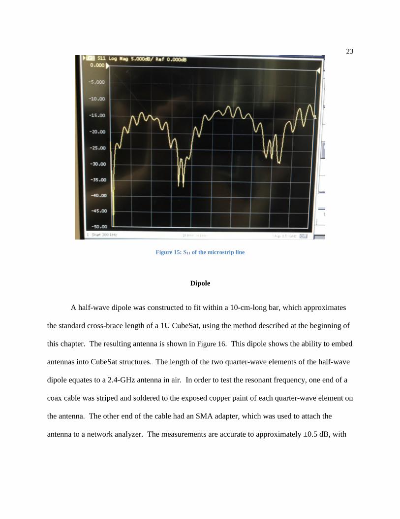
The microstrip line evidenced resonances at 518 MHz and 1.2 GHz, which is consistent
with the expected resonant frequencies for the length of the transmission line. However, the S11
of the microstrip line seen in Figure 16 indicates that the microstrip line matched fairly well with
the 50-Ω system. The VNA measured an impedance of roughly 40 to 50 Ω across its frequency
range, which indicates that the relative dielectric constant for the high temperature resin is
between 5 and 8 [14]. Some noise from cable bend interfered with the measurements. Further
testing is necessary to derive the exact electromagnetic properties.
Figure 13: Microstrip line (Front View)
Figure 14: Microstrip line (Back View)
23
Figure 15: S11 of the microstrip line
Dipole
A half-wave dipole was constructed to fit within a 10-cm-long bar, which approximates
the standard cross-brace length of a 1U CubeSat, using the method described at the beginning of
this chapter. The resulting antenna is shown in Figure 16. This dipole shows the ability to embed
antennas into CubeSat structures. The length of the two quarter-wave elements of the half-wave
dipole equates to a 2.4-GHz antenna in air. In order to test the resonant frequency, one end of a
coax cable was striped and soldered to the exposed copper paint of each quarter-wave element on
the antenna. The other end of the cable had an SMA adapter, which was used to attach the
antenna to a network analyzer. The measurements are accurate to approximately ±0.5 dB, with

24 cable lengths and bending effecting the exact results. The S11 graph in Figure 17 shows that the
resonance of the dipole by itself is approximately 2.72 GHz.
Figure 16: Dipole embedded in resin
Figure 17: S11 of dipole antenna
The dipole was then attached to a mockup of a 3U CubeSat frame to simulate its use as a
cross-brace, as shown in Figure 18. The scattering effect from the metallic structure was
minimal, but should be considered. The S11 of the antenna in this configuration, shown in Figure
100 mm

25 19, indicates a slightly broader bandwidth around 2.6 GHz and a stronger resonances than before
at 1.3 GHz.
Figure 18: Dipole attached to CubeSat frame as cross-brace

26
Figure 19: S11 of dipole in CubeSat frame
Many CubeSats may want to shield their internal components from their antennas and
ensure that the majority of the power radiates away from the satellite. Therefore, it may be
desirable to have a ground plane on the side of the antenna facing the inside of the CubeSat. In
order to simulate this, copper tape was placed on the internal face of the cross-brace with the
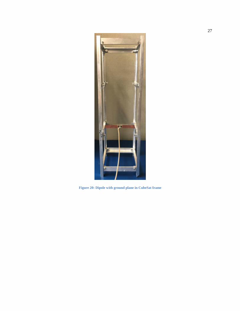
dipole to coax connection, as shown in Figure 20. This new antenna has a strong resonance at
approximately 2.72 GHz, as seen in the S11 graph shown Figure 21.
27
Figure 20: Dipole with ground plane in CubeSat frame

28
Figure 21: S11 of dipole with ground plane in CubeSat frame
29 Chapter 5
Conclusions and Future Work
Summary
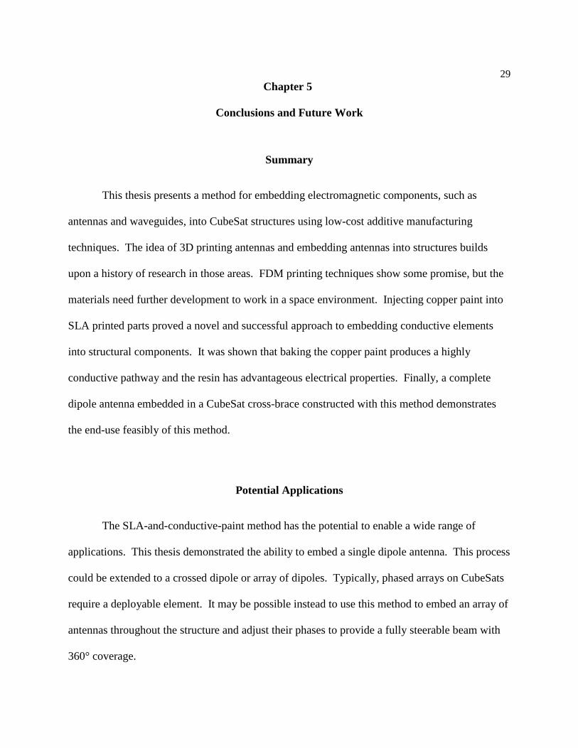
This thesis presents a method for embedding electromagnetic components, such as
antennas and waveguides, into CubeSat structures using low-cost additive manufacturing
techniques. The idea of 3D printing antennas and embedding antennas into structures builds
upon a history of research in those areas. FDM printing techniques show some promise, but the
materials need further development to work in a space environment. Injecting copper paint into
SLA printed parts proved a novel and successful approach to embedding conductive elements
into structural components. It was shown that baking the copper paint produces a highly
conductive pathway and the resin has advantageous electrical properties. Finally, a complete
dipole antenna embedded in a CubeSat cross-brace constructed with this method demonstrates
the end-use feasibly of this method.
Potential Applications
The SLA-and-conductive-paint method has the potential to enable a wide range of
applications. This thesis demonstrated the ability to embed a single dipole antenna. This process
could be extended to a crossed dipole or array of dipoles. Typically, phased arrays on CubeSats
require a deployable element. It may be possible instead to use this method to embed an array of
antennas throughout the structure and adjust their phases to provide a fully steerable beam with
360° coverage.

30 The microstrip test started to show some ability for SLA printed parts to act as
waveguides. Combining this idea with the method of injecting copper into the parts could lead
to waveguides or cabling embedded into the structure to replace coaxial cabling inside the
satellite. Waveguides could also be used for polarizing a signal or matching an antenna. It may
even be possible to print a small horn antenna within the CubeSat structure depending on the size
of the satellite and the required frequency.
While most CubeSats follow a standard configuration and shape, it is not necessary for
all small satellites to follow suit. A cylindrical structure could lend itself to embedding a helical
antenna. The SLA printers could also be used to print out multiple sides of the structure, or even
the whole structure, in one piece. This would allow antennas or waveguides embedded in the
structure to encompass multiple sides. Optimization techniques and fractal designs may yield
further applications in the future.
Future Work
Before it is possible to fully utilize modeling and optimization software such as FEKO,
HFFS, or CST, the electrical properties of the resin must be fully understood. Precise
measurements of the relative permittivity and loss tangent need to be obtained. For use in space,
it is also necessary to take more complete outgassing and water adsorption measurements. To
verify those measurements, prototypes of the applications listed above should be constructed and
test data in an anechoic chamber compared to the model results.
31
BIBLIOGRAPHY
[1] J. Synowiec, “Cubesat Tape Measure UHF Antenna,” Seelio, seelio.com, June 2015.
[2] “3D Printing CubeSat Bodies For Cheaper, Faster Missions,” ESA: Engineering &
Technology, May 2017.
[3] S. Sinha, “Improving Quality of Multi-Functional Structures Created Via Material
Extrusion Additive Manufacturing,” The Pennsylvania State University, M.S. Thesis, May
2017.
[4] J.J. Adams, E.B. Duoss, T.F.Malkowski, M.J. Motala, B.Y. Ahn, R.G. Nuzzo, J.T.
Bernhard, and J.A. Lewis, “Conformal Printing of Electrically Small Antennas on Three-
Dimensional Surfaces,” Advanced Materials, vol. 23, pp. 1335–1340, 2011.
[5] A.G. Lopez and E.E. Lopez C., “Optimization and Fabrication by 3D Printing of a Volcano
Smoke Antenna for UWB Applications,” 7th European Conference on Antennas and
Propagation, April 2013.
[6] P. Nayeri, M. Liang, F.A. Sabory-García, M. Tuo, F. Yang, M. Gehm, H. Xin, and A.Z.
Elsherveni, “3D Printed Dielectric Reflectarrays: Low-Cost High-Gain Antennas at Sub-
Millimeter Waves,” IEEE Transactions on Antennas and Propagation, vol. 62, pp. 2000–
2008, April 2014.
[7] A. Bisognin, D. Titz, F. Ferrero, R. Pilard, C.A. Fernandes, J.R. Costa, C. Corre, F.
Calascibetta, J.M. Riviere, A. Poulain, C. Badard, F. Gianesello, C. Luxey, P. Busson, D.
Gloria, and D. Belot, “3D Printed Plastic 60 GHz Lens: Enabling Innovative Millimeter

32 Wave Antenna Solution and System,” Microwave Symposium (IMS) 2014 IEEE MMT-S
International, June 2014.
[8] J.H. Boicey, “Automobile Windshield of Laminated Glass Having Embedded Antenna
Wires,” US Patent US 3208070 A, 1965.
[9] M.S. Sharawi, D.N. Aloi and O.A. Rawashdeh, “Design and Implementation of Embedded
Printed Antenna Arrays in Small UAV Wing Structures,” IEEE Transactions on Antennas
and Propagation, vol. 58, pp. 2531–2538, May 2010.
[10] P. Keane, C.K. Chua, and S.C. Joshi, “Embedding Electronics in Printing ULTEM 9085
Quadcopter,” Proceedings of the 2nd International Conference on Progress in Additive
Manufacturing (Pro-AM 2016), 2016.
[11] F.C. Gross, “Problems Associated with Nylon Usage on Spacecraft,” NASA: Materials
Engineering Branch, TIP No. 077, Oct. 2002.
[12] The Virtual Foundry, “www.thevirtualfoundry.com/how-it-works.”
[13] “Design Specs,” FormLabs, formlabs.com, 2017.
[14] JSC EP-WI-032 “Statement of Work: Engineering Evaluation Qualification and Flight
Acceptance Tests for Lithium-Ion Cells and Battery Packs for Small Satellite Systems,”
NASA: Johnson Space Center.
[15] “Microstrip Calculator,” Pasternack, www.pasternack.com/t-calculator-microstrip.aspx,
accessed July 2017.

Academic Vita Rebecca Arenson
EDUCATION The Pennsylvania State University, College of Engineering Class of 2017 Schreyer Honors College – Integrated Undergraduate/Graduate Program University Park, PA Masters of Science and Bachelor of Science in Electrical Engineering
Singapore Study Abroad National University of Singapore, Singapore Engineering Design Course May 2014
• Attended 2.5 weeks of intensive courses on engineering design for global markets • Developed a flexible induction cooking system using compliant mechanisms to increase sustainability
Awards • President’s Sparks Award • President’s Freshman Award • Penn State Provost Award
• Lockheed Martin Space Systems Engineering Excellence Award • Clifford B. Holt, Jr. Memorial Scholarship in Electrical Engineering • National Merit Lockheed Martin Academic Scholarship
WORK EXPERIENCE MIT Lincoln Laboratory Lexington, MA RF Engineer, Group 64 September 2017 - present
• Conduct analysis and testing for RF boards in communications systems to meet critical schedule needs • Design, analyze, and test satellite communications ground station terminals • Develop and teach a CubeSat class, including launching a 1U CubeSat
Analyzed Lockheed Martin Corporation Littleton, CO RF Engineer, Space Systems Company May 2016 – August 2016
• Conducted GPSR trade study for small satellites at geosynchronous orbit • Developed a neural network to automatically classify the modulation of an unknown signal from IQ samples • Analyzed the effect of interference on a receiver system • Conducted a heritage review of a communications subsystem and supplier environmental testing • Modeled correlated error for a guidance, navigation, and control simulation • Designed test circuits for high speed digital logic components • Interfaced with vendors, developed purchase orders, and worked on sub-contracts • Modeled the scattered pattern from a drone flying over an antenna
Lockheed Martin Corporation Littleton, CO Antenna Engineer Summer Intern, Space Systems Company May – August 2015
• Received an Engineering Excellence Award for troubleshooting the GPS III V-Sensor through CST modeling to achieve full compliance and avoid a waiver
• Invented a spiral disk antenna over a conic ground plane that is a third of the size of a bicone with a similar pattern but broader band performance
• Created a feed horn catalog to improve the feed horn design process • Developed a common S-band omni antenna for use across multiple programs • Designed and optimized slotted and stacked patch antennas for Athena
Lockheed Martin Corporation

Valley Forge, PA RF Engineer Summer Intern, Space Systems Company June – August 2014
• Conducted RF testing and analysis on flight hardware for the ICBM Mk21 Fuze Refurbishment Program • Performed a Scattering Analysis to support a proposal for the SBIRS program • Developed requirement verification and analysis tools in MATLAB that added to the digital tapestry • Supported presenting data to the customer through MATLAB videos and graphs
LEADERSHIP EXPERIENCE Student Space Programs Laboratory University Park, PA Communications and Ground Station Co-lead, Systems Engineer 8/2015 – 8/2016
• Design, test and implement the communications subsystem for the OSIRIS 3U CubeSat • Develop the interfaces between the OSIRIS 3U CubeSat’s subsystems and guide the team in testing and
building the satellite Institute of Electrical and Electronics Engineers University Park, PA Corporate Liaison 4/2016 – 4/2017
• Organize corporate sponsorships, information sessions, and networking events • Represent IEEE to all corporate entities
Skills • Electromagnetics: CST, CHAMP, GRASP, FEKO, HFSS • Programming: MATLAB, Python, C++, HTML, CSS, LabView • Analog and Digital Circuits: Verilog, Altium, Multisim