Embed Size (px)
Citation preview

EXAMINED BY : FILE NO . CAS-50095
EMERGING DISPLAY ISSUE : MAR.17,1999
APPROVED BY:TECHNOLOGIES CORPORATION
TOTAL PAGE : 28
VERSION : 5
CUSTOMER ACCEPTANCE STANDARD SPECIFICATIONS
MODEL NO . :
FOR MESSRS :
E U - K S 0 0 6 6
CUSTOMER'S APPROVAL
DATE : _____________________________
BY :
_____________________________

E M E R G I N G D I S P L A Y MODEL NO . VERSION
TECHNOLOGIES CORPORATION E U - K S 0 0 6 6 5 DOC . FIRST ISSUE
R E C O R D S OF R E V I S I O N MAY.26 ,1995
D A T EREVISED
PAGENO.
S U M M A R Y
AUG.02,1995 ALL APPEND TIMING OF UMC'S UM3881BAPR.15,1996 5~30 APPEND PAGE 5.
3.4 POWER SUPPLY CONDITIONS USING INTERNAL RESET CIRCUIT .
MAR.17,1999 24~31 CHANGED “ ROM CODE “OCT.29,1999 2 3. ELECTRICAL CHARACTERISTICS
ADD 3.1.1 DC CHARACTERISTICS FOR KS0066(VDD=2.7V~4.5V) 3.2 AC TIMING CHARACTERISTICSADD 3.2.2 FOR KS0066(VDD=2.7V~4.5V)
E M E R G I N G D I S P L A Y MODEL NO . VERSION
TECHNOLOGIES CORPORATION E U - K S 0 0 6 6 5
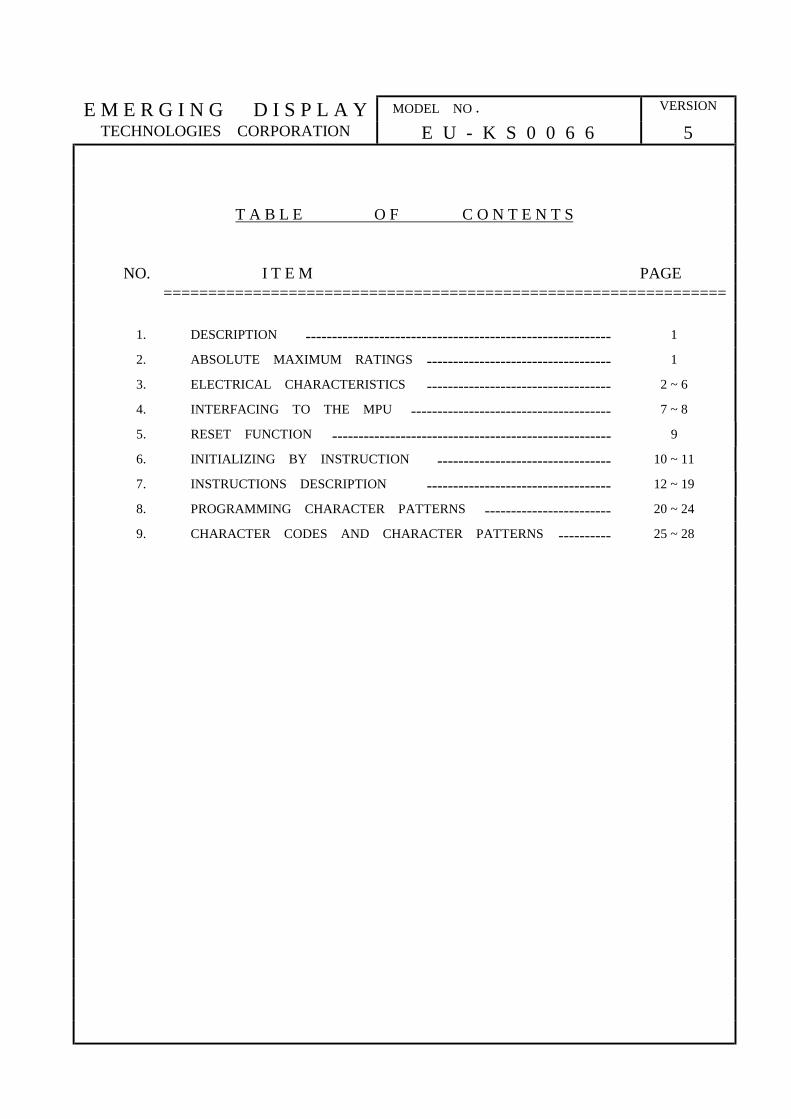
T A B L E O F C O N T E N T S
NO. I T E M PAGE ===============================================================
1. DESCRIPTION ---------------------------------------------------------- 1
2. ABSOLUTE MAXIMUM RATINGS ----------------------------------- 1
3. ELECTRICAL CHARACTERISTICS ----------------------------------- 2 ~ 6
4. INTERFACING TO THE MPU -------------------------------------- 7 ~ 8
5. RESET FUNCTION ----------------------------------------------------- 9
6. INITIALIZING BY INSTRUCTION --------------------------------- 10 ~ 11
7. INSTRUCTIONS DESCRIPTION ----------------------------------- 12 ~ 19
8. PROGRAMMING CHARACTER PATTERNS ------------------------ 20 ~ 24
9. CHARACTER CODES AND CHARACTER PATTERNS ---------- 25 ~ 28

E M E R G I N G D I S P L A Y MODEL NO . VERSION PAGE
TECHNOLOGIES CORPORATION E U - K S 0 0 6 6 5 1
1. DESCRIPTION
The KS0066(for controller IC KS0066,UM3881,SED1278 ) dot-matrix liquid crystaldisplay controller and driver LSI displays alphanumerics, Japanese kana characters,and symbols. It can be configured to drive a dot-matrix liquid crystal displayunder the control of a 4- or 8- bit microprocessor. Since all the functions such asdisplay RAM, character generator, and liquid crystal driver, required for driving adot-matrix liquid crystal display are internally provided on one chip, a minimalsystem can be interfaced with this controller/driver.
The KS0066 character generator ROM is extended to generate 192 5 x 8 dotcharacter fonts and 32 5 x 10 dot character fonts for a total of 224 different characterfonts.
2. ABSOLUTE MAXIMUM RATINGS
ITEM SYMBOL VALUE UNIT
POWER SUPPLY VOLTAGE ( 1 ) VDD-GND -0.3 TO +7.0 V
POWER SUPPLY VOLTAGE ( 2 ) VO-GND VDD-13.5 ~ VDD+0.3 V
INPUT VOLTAGE VI -0.3 TO VDD+0.3 V
Note: If the LSI is used above these absolute maximum ratings, it may becomepermanently damaged. Using the LSI within the following electrical characteristiclimits is strongly recommended for normal operation. If these electricalcharacteristic conditions are also exceeded, the LSI will malfunction and cause poorreliability.

E M E R G I N G D I S P L A Y MODEL NO . VERSION PAGE
TECHNOLOGIES CORPORATION E U - K S 0 0 6 6 5 2
3. ELECTRICAL CHARACTERISTICS3.1 DC CHARACTERISTICS FOR SED1278,UM3881,KS0066(VDD=4.5V~5.5V)
ITEM SYMBOL MIN TYP MAX UNIT TEST CONDITION
OPERATING VOLTAGE VDD 4.5 5.0 5.5 V
INPUT HIGH VOLTAGE VIH1 2.2 VDD V
INPUT LOW VOLTAGE VIL1 -0.3 0.6 V
OUTPUT HIGH VOLTAGE(1) ( DB0-DB7 )
VOH1 2.4__ __ V -IOH = 0.205 mA
OUTPUT LOW VOLTAGE (1) ( DB0-DB7 )
VOL1__ __ 0.4 V IOL = 1.2 mA
INPUT LEAKAGE CURRENT IL1 -1 1 µA VIN = 0 TO VDD
PULL-UP MOS CURRENT ( DB0-DB7 , RS , R/W)
-IP 50 125 250 µA VDD = 5 V
POWER SUPPLY CURRENT ICC __ 0.35 0.60 mA
Rf OSCILLATION EXTERNAL CLOCK
VDD=5V fosc=270KHZ
3.1.1 DC CHARACTERISTICS FOR KS0066(VDD=2.7V~4.5V)ITEM SYMBOL MIN TYP MAX UNIT TEST CONDITION
OPERATING VOLTAGE VDD 2.7 4.5 V
INPUT HIGH VOLTAGE VIH1 0.7*VDD VDD V
INPUT LOW VOLTAGE VIL1 -0.3 0.55 V
OUTPUT HIGH VOLTAGE(1) ( DB0-DB7 )
VOH1 0.75*VDD__ __ V -IOH = 0.1 mA
OUTPUT LOW VOLTAGE (1) ( DB0-DB7 )
VOL1__ __ 0.2*VDD V IOL = 0.1 mA
INPUT LEAKAGE CURRENT IL1 -1 1 µA VIN = 0 TO VDD
PULL-UP MOS CURRENT ( DB0-DB7 , RS , R/W)
-IP 10 50 120 µA VDD = 3 V
POWER SUPPLY CURRENT ICC __ 0.15 0.3 mA
Rf OSCILLATION EXTERNAL CLOCK
VDD=3V fosc=270KHZ

E M E R G I N G D I S P L A Y MODEL NO . VERSION PAGE
TECHNOLOGIES CORPORATION E U - K S 0 0 6 6 5 3
3.2 AC TIMING CHARACTERISTICS3.2.1 FOR SED1278,KS0066(VDD=4.5V~5.5V)
WRITE OPERATIONITEM SYMBOL MIN TYP MAX UNIT TEST CONDITION
ENABLE CYCLE TIME tcycE 500 ns FIGURE 1
ENABLE PULSE WIDTH ( HIGH LEVEL )
PWEH 220 ns
ENABLE RISE/FALL TIME tEr , tEf 25 ns
ADDRESS SET-UP TIME ( RS , R/W TO E )
Tas 40 ns
ADDRESS HOLD TIME Tah 10 ns
DATA SET-UP TIME Tdsw 60 ns
DATA HOLD TIME Th 10 ns
READ OPERATIONITEM SYMBOL MIN TYP MAX UNIT TEST CONDITION
ENABLE CYCLE TIME tcycE 500 ns FIGURE 2
ENABLE PULSE WIDTH ( HIGH LEVEL )
PWEH 220 ns
ENABLE RISE/FALL TIME tEr , tEf 25 ns
ADDRESS SET-UP TIME ( RS , R/W TO E )
Tas 40 ns
ADDRESS HOLD TIME Tah 10 ns
DATA DELAY TIME Tddr 60 120 ns
DATA HOLD TIME Tdhr 20 ns
3.2.2 FOR KS0066(VDD=2.7V~4.5V) WRITE OPERATION
ITEM SYMBOL MIN TYP MAX UNIT TEST CONDITION ENABLE CYCLE TIME tcycE 1000 ns FIGURE 1
ENABLE PULSE WIDTH ( HIGH LEVEL )
PWEH 450 ns
ENABLE RISE/FALL TIME tEr , tEf 25 ns
ADDRESS SET-UP TIME ( RS , R/W TO E )
Tas 60 ns
ADDRESS HOLD TIME Tah 20 ns
DATA SET-UP TIME Tdsw 195 ns
DATA HOLD TIME Th 10 ns
READ OPERATIONITEM SYMBOL MIN TYP MAX UNIT TEST CONDITION
ENABLE CYCLE TIME tcycE 1000 ns FIGURE 2
ENABLE PULSE WIDTH ( HIGH LEVEL )
PWEH 450 ns
ENABLE RISE/FALL TIME tEr , tEf __ __ 25 ns
ADDRESS SET-UP TIME ( RS , R/W TO E )
Tas 60 ns
ADDRESS HOLD TIME Tah 20 ns
DATA DELAY TIME Tddr 360 ns
DATA HOLD TIME Tdhr 5 ns

E M E R G I N G D I S P L A Y MODEL NO . VERSION PAGE
TECHNOLOGIES CORPORATION E U - K S 0 0 6 6 5 4
3.2.3 FOR UM3881 WRITE OPERATION
ITEM SYMBOL MIN TYP MAX UNIT TEST CONDITION
ENABLE CYCLE TIME tcycE 500 ns FIGURE 1
ENABLE PULSE WIDTH ( HIGH LEVEL )
PWEH 300 __ __ ns
ENABLE RISE/FALL TIME tEr , tEf 25 ns
ADDRESS SET-UP TIME tAS 60 ns 8bit OPERATION MODE
( RS , R/W TO E ) 100 ns 4bit OPERATION MODE
ADDRESS HOLD TIME tAH 10 ns
DATA SET-UP TIME tDSW 100 ns
DATA HOLD TIME tH 10 ns
READ OPERATIONITEM SYMBOL MIN TYP MAX UNIT TEST CONDITION
ENABLE CYCLE TIME tcycE 500 ns FIGURE 2
ENABLE PULSE WIDTH ( HIGH LEVEL )
PWEH 300 ns
ENABLE RISE/FALL TIME tEr , tEf 25 ns
ADDRESS SET-UP TIME tAS 60 ns 8bit OPERATION MODE
( RS , R/W TO E ) 100 ns 4bit OPERATION MODE
ADDRESS HOLD TIME tAH 10 __ ns
DATA DELAY TIME tDDR 190 ns
DATA HOLD TIME tDHR 20 ns

E M E R G I N G D I S P L A Y MODEL NO . VERSION PAGE
TECHNOLOGIES CORPORATION E U - K S 0 0 6 6 5 5
3.3 TIMING CHARACTERISTICS3.3.1 WRITE OPERATION
RS
R/W
E
DB0〜DB7
VIH1
VIL1
tAS
VIL1
V IH1
VIL1
PW EH
VIH1 VIH1
VIL1 VIL1 VIL1
VIL1VIL1
VIH1 VIH1Valid data
tAH
AHt
t
t t
t cycE
DSWEr Ht
Ef
FIGURE 1 WRITE OPERATION
3.3.2 READ OPERATION
R S
R /W
E
D B 0〜D B 7
V IH 1
V IL1
tA S
V IH 1
V IL1
PW E H
V IH 1 V IH 1
V IL1 V IL1 V IL 1
V alid data
t A H
A Ht
t
tt
t cycE
E r
V IH 1 V IH 1
E f
D D R tD H R
V O H 1*
V O L1
*V O H 1
V O L1
FIGURE 2 READ OPERATION

E M E R G I N G D I S P L A Y MODEL NO . VERSION PAGE
TECHNOLOGIES CORPORATION E U - K S 0 0 6 6 5 6
3.4 POWER SUPPLY CONDITIONS USING INTERNAL RESET CIRCUIT
ITEM SYMBOL MIN TYP MAX UNIT
POWER SUPPLY RISE TIME trCC 0.1 10 ms
POWER SUPPLY OFF TIME tOFF 1 ms
trcc
Vcc 4.5 V *2
0.2 V 0.2V 0.2V
tOFF*1
t OFF0.1 ms ≤ trcc≤10 ms ≥ 1 ms
Note:1. tOFF compensates for the power oscillation period causedby momentary power supply oscillations.
2. Specified at 4.5V for Vcc=5v operation.3. For if 4.5V is not reached during 5V operation, the
internal reset circuit will not operate normally.In this case, the LSI must be initialized by software.( Refer to the initializing by instruction section. )

E M E R G I N G D I S P L A Y MODEL NO . VERSION PAGE
TECHNOLOGIES CORPORATION E U - K S 0 0 6 6 5 7
4. INTERFACING TO THE MPU
The KS0066 can send data in either two 4-bit operations or one 8-bit operation, thusallowing interfacing with 4- or 8-bit MPUs.
* For 4-bit interface data, only four bus lines ( DB4 to DB7 ) are used for transfer.Bus lines DB0 to DB3 are disabled. The data transfer between the KS0066 and theMPU is completed after the 4-bit data has been transferred twice. As for the order ofdata transfer, the four high order bits ( for 8-bit operation, DB4 to DB7 ) aretransferred before the four low order bits ( for 8-bit operation, DB0 to DB3 )
The busy flag must be checked ( one instruction ) after the 4-bit data has beentransferred twice. Two more 4-bit operations then transfer the busy flag and addresscounter data.
* For 8-bit interface data, all eight bus lines ( DB0 to DB7 ) are used.
DATA DATANOTBUSYBUSY BUSY
FUNCTIONINGINTERNALOPERATIO
DB7
E
RS
R/W
INSTRUCTIONWRITE
BUSY FLAGCHECK
BUSY FLAGCHECK
BUSY FLAGCHECK
INSTRUCTIONWRITE
������������������������������������������������
���������������������������������������������������������
���������������������������������������������������������������������������������������������
���������������������������������������������������������������������������������������������
���������������������������������������������������������������������
������������������������������
FIGURE 3 EXAMPLE OF BUSY FLAG CHECK TIMING SEQUENCE
FIGURE 4 4-BIT TRANSFER EXAMPLE
IR7 IR3 BF AC3 DR7 DR3DB7
IR6 IR2 AC6 AC2 DR6 DR2DB6
IR5 IR1 AC5 AC1 DR5 DR1DB5
IR4 IR0 AC4 AC0 DR4 DR0DB4
E
R/W
RS
INSTRUCTION REGISTER ( IR )WRITE
BUSY FLAG ( BF ) ANDADDRESS COUNTER ( AC )READ
DATA REGISTER ( DR )READ

E M E R G I N G D I S P L A Y MODEL NO . VERSION PAGE
TECHNOLOGIES CORPORATION E U - K S 0 0 6 6 5 8
FIGURE 5 EXAMPLE OF 4-BIT DATA TRANSFER TIMING SEQUENCE
FUNCTIONINGINTERNALOPERATION
DB7
E
RS
R/W
INSTRUCTIONWRITE
BUSY FLAGCHECK
BUSY FLAGCHECK
INSTRUCTIONWRITE
��������������������������
��������������������������������������������
������������������������������������������
������������������������������������
��������������������������������D3D7AC3
NOTBUSYAC3BUSYIR3IR7
NOTE : *IR7, IR3 ARE THE 7TH AND 3RD BITS OF THE INSTRUCTION AC3 IS THE 3RD BIT OF THE ADDRESS COUNTER

E M E R G I N G D I S P L A Y MODEL NO . VERSION PAGE
TECHNOLOGIES CORPORATION E U - K S 0 0 6 6 5 9
5. RESET FUNCTIONINITIALIZING BY INTERNAL RESET CIRCUIT
An internal reset circuit automadtically initializes the KS0066 when the power isturned on. The following instructions are executed during the initialization. The busyflag ( BF ) is kept in the busy state until the initialization ends ( BF = 1 ). The busystate lasts for 10 ms after Vcc rises to 4.5 V.
1. Display clear2. Function set : DL = 1; 8-bit interface data N = 0; 1-line display F = 0; 5 x 8 dot character font3. Display on/off control : D = 0; Display off C = 0; Cursor off B = 0; Blinking off4. Entry mode set : I/D = 1; Increment by 1 S = 0; No shift
Note :If the electrical characteristics conditions listed under the table Power SupplyConditions Using Internal Reset Circuit are not met, the internal reset circuitwill not operate normally and will fail to initialize the KS0066. For such a case,initialization must be performed by the MPU as explained in the section,Initializing by Instruction.

E M E R G I N G D I S P L A Y MODEL NO . VERSION PAGE
TECHNOLOGIES CORPORATION E U - K S 0 0 6 6 5 10
6. INITIALIZING BY INSTRUCTIONIf the power supply conditions for correctly operating the internal reset circuit are notmet, initialization by instructions becomes necessary.Refer to 6-1 and 6-2 for the procedures on 8-bit and 4-bit initializations, respectively.
6-1 8-BIT INTERFACE
Power on
Wait for more than 15 ms after Vcc rises to 4.5 V
RSR/WDB7DB6DB5 DB4DB3DB2DB1DB0
****110000
Wait for more than 4.1 ms
RSR/WDB7DB6DB5DB4DB3DB2DB1DB0****110000
Wait for more than 100 µs
RSR/WDB7DB6DB5DB4DB3DB2DB1DB0****110000
RSR/WDB7DB6DB5DB4DB3DB2DB1DB0**110000 N F
0000 00 1 0 00
0000 00 0 0 10
0000 00 0 1 SI/D
Wait for more than 40 ms after Vcc rises to 2.7 V
BF cannot be checked before this instruction.
Function set ( Interface is 8 bits long. )
BF cannot be checked before this instruction.
Function set ( Interface is 8 bits long. )
BF cannot be checked before this instruction.
Function set ( Interface is 8 bits long. )
BF can be checked after the following instructions.When BF is not checked, the waiting time betweeninstructions is longer than the execution instuctiontime. ( See table 3. )
Function set ( Interface is 8 bits long. Specify thenumber of display lines and character font. )The number of display lines and character fontcannot be changed after this point.
Display off
Entry mode setInitialization ends
Display clear

E M E R G I N G D I S P L A Y MODEL NO . VERSION PAGE
TECHNOLOGIES CORPORATION E U - K S 0 0 6 6 5 11
6-2 4-BIT INTERFACEPower on
Wait for more than 15 ms after Vcc rises to 4.5 V
RS R/W DB7 DB6 DB5 DB4110000
Wait for more than 4.1 ms
Wait for more than 100 µs
Wait for more than 40 ms after Vcc rises to 2.7 V
BF cannot be checked before this instruction.
Function set ( Interface is 8 bits long. )
BF cannot be checked before this instruction.
Function set ( Interface is 8 bits long. )
BF cannot be checked before this instruction.
Function set ( Interface is 8 bits long. )
BF can be checked after the following instructions.When BF is not checked, the waiting time betweeninstructions is longer than the execution instuctiontime. ( See table 3. )
Function set ( Interface is 4 bits long. Specify thenumber of display lines and character font. )The number of display lines and character fontcannot be changed after this point.
Display off
Display clear
Entry mode setInitialization ends
RS R/W DB7 DB6 DB5 DB4110000
RS R/W DB7 DB6 DB5 DB4110000
RS R/W DB7 DB6 DB5 DB4010000
010000**FN00
000000000100
000000100000
000000SI/D1000
Function set ( Set interface to be 4 bits long. )Interface is 8 bits in length.
E M E R G I N G D I S P L A Y MODEL NO . VERSION PAGE
TECHNOLOGIES CORPORATION E U - K S 0 0 6 6 5 12
7. INSTRUCTION DESCRIPTION
OUTLINE
Only the instruction register ( IR ) and the data register ( DR ) of the KS0066 can becontrolled by the MPU. Before starting the internal operation of the KS0066, controlinformation is temporarily stored into these registers to allow interfacing withvarious MPUs, which operate at different speeds, or various peripheral controldevices. The internal operation of the KS0066 is determined by signals sent from theMPU. These signals, which include register selection signal ( RS ), read/write signal
( R/W ), and the data bus ( DB0 to DB7 ), make up the KS0066 instructions ( table1 ). There are four categories of instructions that :
• Designate KS0066 functions, such as display format, data length, etc.
• Set internal RAM addresses
• Perform data transfer with internal RAM
• Perform miscellaneous functions
Normally, instructions that perform data transfer with internal RAM are used themost. However, auto-incrementation by 1 ( or auto-decrementation by 1 ) of internalKS0066 RAM addresses after each data write can lighten the program load of theMPU. Since the display shift instruction ( table 1 ) can perform concurrently withdisplay data write, the user can minimize system development time with maximumprogramming efficiency.
When an instruction is being executed for internal operation, no instruction otherthan the busy flag/address read instruction can be executed.
Because the busy flag is set to 1 while an instruction is being executed, check it tomake sure it is 0 before sending another instruction from the MPU.
Note :Be sure the KS0066 is not in the busy state ( BF = 0 ) before sending aninstruction from the MPU to the KS0066. If an instruction is sent withoutchecking the busy flag, the time between the first instruction and nextinstruction will take much longer than the instruction time itself. Refer totable 3 for the list of each instruction execution time.
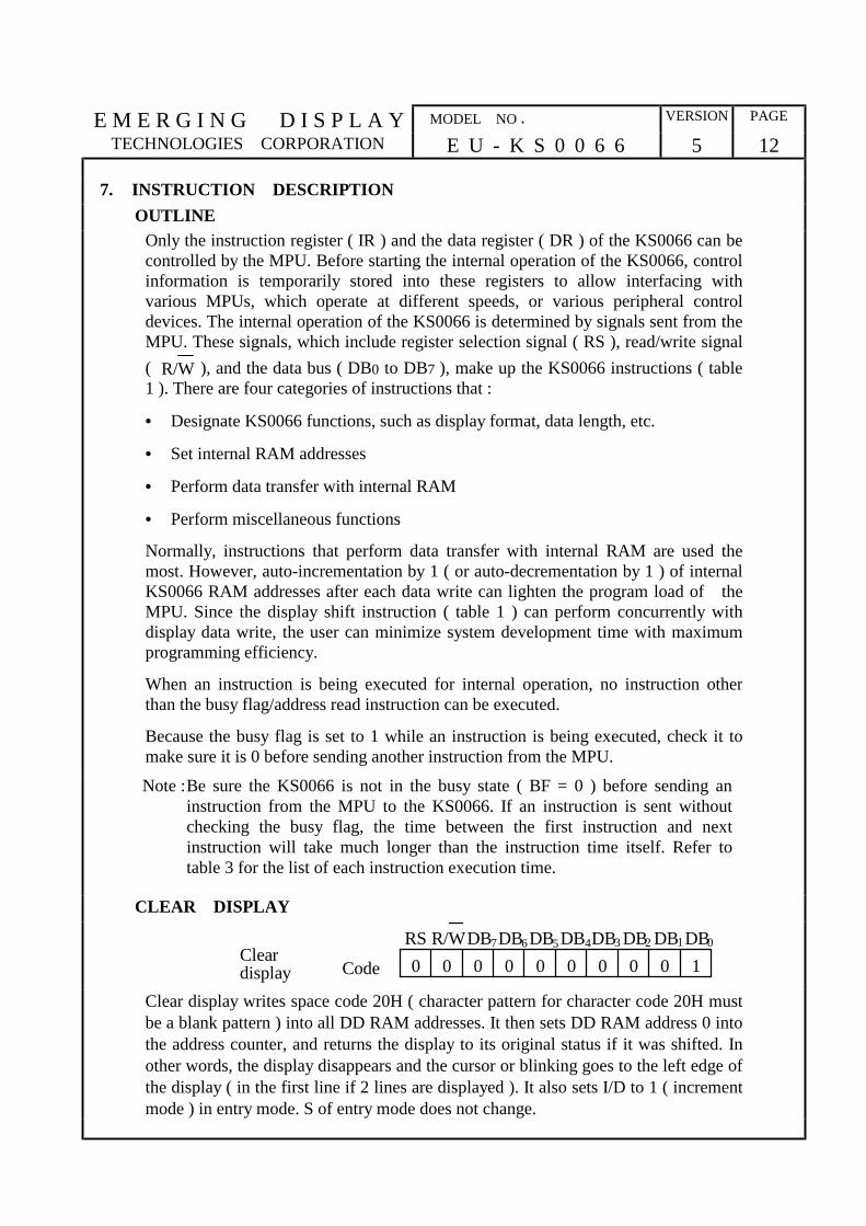
CLEAR DISPLAY
0 0 0 0 0 0 0 0
R/W
0 1
RS DB7DB6DB5DB4DB3 DB2 DB1DB0
CodeCleardisplay
Clear display writes space code 20H ( character pattern for character code 20H mustbe a blank pattern ) into all DD RAM addresses. It then sets DD RAM address 0 intothe address counter, and returns the display to its original status if it was shifted. Inother words, the display disappears and the cursor or blinking goes to the left edge ofthe display ( in the first line if 2 lines are displayed ). It also sets I/D to 1 ( incrementmode ) in entry mode. S of entry mode does not change.

E M E R G I N G D I S P L A Y MODEL NO . VERSION PAGE
TECHNOLOGIES CORPORATION E U - K S 0 0 6 6 5 13
RETURN HOME
0 0 0 0 0 0 0 0
R/W
1 *
RS DB7 DB6 DB5 DB4 DB3 DB2 DB1 DB0
CodeReturnhome Note :*Don’t care.
Return home sets DD RAM address 0 into the address counter, and returns thedisplay to its original status if it was shifted. The DD RAM contents do not change.
The cursor or blinking go to the left edge of the display ( in the first line if 2 lines aredisplayed ).
ENTRY MODE SET
0 0 0 0 0 0 0 1
R/W
I/D S
RS DB7 DB6 DB5 DB4 DB3 DB2 DB1 DB0
CodeEntrymode set
I/D::::Increments ( I/D = 1 ) or decrements ( I/D = 0 ) the DD RAM address by 1 whena character code is written into or read from DD RAM.
The cursor or blinking moves to the right when incremented by 1 and to the left whendecremented by 1. The same applies to writing and reading of CG RAM.
S::::Shift the entire display either to the right ( I/D = 0 ) or to the left ( I/D = 1 ) whenS is 1. The display does not shift if S is 0.
If S is 1, it will seem as if the cursor does not move but the display does. The displaydoes not shift when reading from DD RAM. Also, writing into or reading out fromCG RAM does not shift the display.
DISPLAY ON/OFF CONTROL
0 0 0 0 0 0 1 D
R/W
C B
RS DB7DB6DB5DB4DB3DB2DB1DB0
CodeDisplayon/off control
D::::The display is on when D is 1 and off when D is 0. When off, the display dataremains in DD RAM, but can be displayed instantly by setting D to 1.
C::::The cursor is displayed when C is 1 and not displayed when C is 0. Even if thecursor disappears, the function of I/D or other specifications will not change duringdisplay data write. The cursor is displayed using 5 dots in the 8th line for 5 x 8 dotcharacter font selection and in the 11th line for the 5 x 10 dot character font selection( figure 6 ).
B::::The character indicated by the cursor blinks when B is 1 ( figure 6 ). The blinkingis displayed as switching between all blank dots and displayed characters at a speedof 409.6-ms intervals when fcp or fosc is 250 kHZ. The cursor and blinking can beset to display simultaneously. ( The blinking frequency changes according to fosc orthe reciprocal of fcp. For example, when fcp is 270 kHZ, 409.6 x 250 / 270 = 379.2ms. )

E M E R G I N G D I S P L A Y MODEL NO . VERSION PAGE
TECHNOLOGIES CORPORATION E U - K S 0 0 6 6 5 14
5 x 8 dotcharacter font
5 x 10 dotcharacter font
Cursor display example
Alternating display
Blink display example
FIGURE 6 CURSOR AND BLINKING
cursor
CURSOR OR DISPLAY SHIFT
0 0 0 0 0 1 S/C R/L
R/W
*
RS DB7 DB6 DB5 DB4 DB3 DB2 DB1 DB0
CodeCursor ordisplay shift Note : * Don’t care.*
Cursor or display shift shifts the cursor position or display to the right or left withoutwriting or reading display data ( table 1 ). This function is used to correct or searchthe display. In a 2-line display, the cursor moves to the second line when it passes the40th digit of the first line. Note that the first and second line displays will shift at thesame time.
When the displayed data is shifted repeatedly each line moves only horizontally. Thesecond line display does not shift into the first line position.
The address counter ( AC ) contents will not change if the only action performed is adisplay shift.
TABLE 1 SHIFT FUNCTION
S/C R/L
0 0 SHIFTS THE CURSOR POSITION TO THE LEFT. ( AC IS DECREMENTED BY ONE. )
0 1 SHIFTS THE CURSOR POSITION TO THE RIGHT. ( AC IS INCREMENTED BY ONE. )
1 0 SHIFTS THE ENTIRE DISPLAY TO THE LEFT. THE CURSOR FOLLOWS THE DISPLAY SHIFT.
1 1 SHIFTS THE ENTIRE DISPLAY TO THE RIGHT. THE CURSOR FOLLOWS THE DISPLAY SHIFT.

E M E R G I N G D I S P L A Y MODEL NO . VERSION PAGE
TECHNOLOGIES CORPORATION E U - K S 0 0 6 6 5 15
FUNCTION SET
0 0 0 0 1 DL N F
R/W
*
RS DB7 DB6 DB5 DB4 DB3 DB2 DB1 DB0
CodeFunction set Note : * Don’t care.*
DL : Sets the interface data length. Data is sent or received in 8-bit lengths (DB7 toDB0 ) when DL is 1, and in 4-bit lengths ( DB7 to DB4 ) when DL is 0.
When 4-bit length is selected, data must be sent or received twice.
N : Sets the number of display lines.
F : Sets the character font.
Note :Perform the function at the head of the program before executing anyinstructions ( except for the read busy flag and address instruction ). From thispoint, the function set instruction cannot be executed unless the interface datalength is changed.
TABLE 2 FUNCTION SET
N F NO. OF
DISPLAY LINES
CHARACTERFONT
DUTY FACTOR
REMARKS
0 0 1 5 X 8 DOTS 1/80 1 1 5 X 10 DOTS 1/11
1 * 2 5 X 8 DOTS 1/16 CANNOT DISPLAY TWO LINES FOR 5 X 10 DOT CHARACTER FONT
Note : * Indicates don’t care.
SET CG RAM ADDRESS
0 0 0 1 A A A A
R/WRS DB7 DB6 DB5 DB4 DB3 DB2 DB1 DB0
CodeSet CGRAM address A A
Lowerorder bit
Higherorder bit
Set CG RAM address sets the CG RAM address binary AAAAAA into the addresscounter.
Data is then written to or read from the MPU for CG RAM.
E M E R G I N G D I S P L A Y MODEL NO . VERSION PAGE
TECHNOLOGIES CORPORATION E U - K S 0 0 6 6 5 16
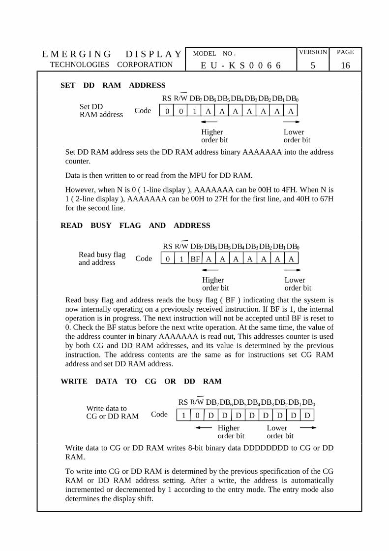
SET DD RAM ADDRESS
0 0 1 A A A A A
R/WRS DB7 DB6 DB5 DB4 DB3 DB2 DB1 DB0
CodeSet DDRAM address A A
Lowerorder bit
Higherorder bit
Set DD RAM address sets the DD RAM address binary AAAAAAA into the addresscounter.
Data is then written to or read from the MPU for DD RAM.
However, when N is 0 ( 1-line display ), AAAAAAA can be 00H to 4FH. When N is1 ( 2-line display ), AAAAAAA can be 00H to 27H for the first line, and 40H to 67Hfor the second line.
READ BUSY FLAG AND ADDRESS
0 1 BF A A A A A
R/WRS DB7 DB6 DB5 DB4 DB3 DB2 DB1 DB0
CodeRead busy flagand address A A
Lowerorder bit
Higherorder bit
Read busy flag and address reads the busy flag ( BF ) indicating that the system isnow internally operating on a previously received instruction. If BF is 1, the internaloperation is in progress. The next instruction will not be accepted until BF is reset to0. Check the BF status before the next write operation. At the same time, the value ofthe address counter in binary AAAAAAA is read out, This addresses counter is usedby both CG and DD RAM addresses, and its value is determined by the previousinstruction. The address contents are the same as for instructions set CG RAMaddress and set DD RAM address.
WRITE DATA TO CG OR DD RAM
1 0 D D D D D
R/WRS DB7DB6DB5DB4DB3DB2DB1DB0
CodeWrite data toCG or DD RAM D D
Lowerorder bit
Higherorder bit
D
Write data to CG or DD RAM writes 8-bit binary data DDDDDDDD to CG or DDRAM.
To write into CG or DD RAM is determined by the previous specification of the CGRAM or DD RAM address setting. After a write, the address is automaticallyincremented or decremented by 1 according to the entry mode. The entry mode alsodetermines the display shift.

E M E R G I N G D I S P L A Y MODEL NO . VERSION PAGE
TECHNOLOGIES CORPORATION E U - K S 0 0 6 6 5 17
READ DATA FROM CG OR DD RAM
1 1 D D D D D
R/WRS DB7 DB6 DB5 DB4 DB3 DB2 DB1 DB0
CodeRead data fromCG or DD RAM D D
Lowerorder bit
Higherorder bit
D
Read data from CG or DD RAM reads 8-bit binary data DDDDDDDD from CG orDD RAM.
The previous designation determines whether CG or DD RAM is to be read. Beforeentering this read instruction, either CG RAM or DD RAM address set instructionmust be executed. If not executed, the first read data will be invalid. When seriallyexecuting read instructions, the next address data is normally read from the secondread. The address set instructions need not be executed just before this readinstruction when shifting the cursor by the cursor shift instruction ( when reading outDD RAM ). The operation of the cursor shift instruction is the same as the set DDRAM address instruction.
After a read, the entry mode automatically increases or decreases the address by 1.However, display shift is not executed regardless of the entry mode.
Note :The address counter ( AC ) is automatically incremented or decremented by 1after the write instructions to CG RAM or DD RAM are executed. The RAMdata selected by the AC cannot be read out at this time even if read instructionsare executed. Therefore, to correctly read data, execute either the address setinstruction or cursor shift instruction ( only with DD RAM ), then just beforereading the desired data, execute the read instruction from the second time theread instruction is sent.

E M E R G I N G D I S P L A Y MODEL NO . VERSION PAGE
TECHNOLOGIES CORPORATION E U - K S 0 0 6 6 5 18
TABLE 3 INSTRUCTIONS
CODE EXECUTION
INSTRUCTION RS R/W DB7 DB6 DB5 DB4 DB3 DB2 DB1 DB0 DESCRIPTION
TIME (MAX)
(WHEN fcp
OR fosc IS 250 KHZ
Clear display
0 0 0 0 0 0 0 0 0 1 Clears entire display and sets DD RAM address 0 in address counter.
1.64 ms
Return home
0 0 0 0 0 0 0 0 1
Sets DD RAM address 0 in address counter. Also returns display from being shifted to original position. DD RAM contents remain unchanged.
1.64 ms
Entry mode set
0 0 0 0 0 0 0 1 I/D S
Sets cursor move direction and specifies display shift. These operations are performed during data write and read.
40 µs
Display on/off control
0 0 0 0 0 0 1 D C B
Sets entire display ( D ) on/off, cursor on/off ( C ), and blinking of cursor position character ( B ).
40 µs
Cursor or display shift
0 0 0 0 0 1 S/C R/L Moves cursor and shifts display without changing DD RAM contents.
40 µs
Function set
0 0 0 0 1 DL N F
Sets interface data length ( DL ), number of display lines ( N ), and character font ( F ).
40µs
Set CG RAM address
0 0 0 1 ACG ACG ACG ACG ACG ACG
Sets CG RAM address CG RAM data is sent and received after this setting.
40 µs
Set DD RAM address
0 0 1 ADD ADD ADD ADD ADD ADD ADD
Sets DD RAM address. DD RAM data is sent and received after this setting.
40 µs
Read busy flag & address
0 1 BF AC AC AC AC AC AC AC
Reads busy flag ( BF ) indicating internal operation is being performed and reads address counter contents.
0 µs

E M E R G I N G D I S P L A Y MODEL NO . VERSION PAGE
TECHNOLOGIES CORPORATION E U - K S 0 0 6 6 5 19
TABLE 3 INSTRUCTIONS ( CONT )
CODE EXECUTION
INSTRUCTION RS R/W DB7 DB6 DB5 DB4 DB3 DB2 DB1 DB0 DESCRIPTION
TIME (MAX)
(WHEN fcp
OR fosc IS 250 KHZ
Write data to CG or DD RAM
1 0 Write data Writes data into DD RAM or CG RAM.
37 µs
tADD = 4µs*
Read data from CG or DD RAM
1 1 Read data Reads data from DD RAM or CG RAM.
37 µs
tADD = 4µs*
I/D = 1 : Increment I/D = 0 : Decrement S = 1 : Accompanies display shift S/C= 1 : Display shift S/C= 0 : Cursor move R/L= 1 : Shift to the right R/L= 0 : Shift to the left DL = 1 : 8 bits, DL = 0 : 4 bits N = 1 : 2 lines, N = 0 : 1 line F = 1 : 5 X 10 dots, F = 0 : 5 X 8 dots BF = 1 : Internally operating BF = 0 : Instructions acceptable
DD RAM : Display data RAM CG RAM : Character generator RAM ACG : CG RAM address ADD : DD RAM address ( corresponds to cursor address ) AC : Address counter used for both DD and CG RAM addresses
Note :-- indicates no effect.* After execution of the CG RAM/DD RAM data write or read instruction, theRAM address counter is incremented or decremented by 1. The RAM addresscounter is updated after the busy flag turns off. In figure 7, tADD is the timeelapsed after the busy flag turns off until the address counter is updated.
A A+1
Busy stateBusy signal( DB pin )7
Address counter( DB to DB ins )0 6
Note : tADD depends on the operation frequencytADD = 1.5/ ( fcp or fosc ) seconds
tADD
FIGURE 7 ADDRESS COUNTER UPDATE

E M E R G I N G D I S P L A Y MODEL NO . VERSION PAGE
TECHNOLOGIES CORPORATION E U - K S 0 0 6 6 5 20
8. PROGRAMMING CHARACTER PATTERNS
This section explains the correspondence between addresses and data used toprogram character patterns in EPROM. The KS0066 character generator ROM cangenerate 192 5 x 8 dot character patterns and 32 5 x 10 dot character patterns for atotal of 224 different character patterns.
EPROM address data and character pattern data correspond with each other to form a5 x 8 or 5 x 10 dot character pattern ( tables 4 and 5 )
HANDLING UNUSED CHARACTER PATTERNS
1.
2.
3.
EPROM data outside the character pattern area : Always input 0s.
EPROM data in CG RAM area : Always input 0s. ( Input 0s to EPROM addresses00H to FFH. )
EPROM data used when the user does not use any KS0066 character pattern :According to the user application, handled in one of the two ways listed as follows.
(1)
(2)
When unused character patterns are not programmed : If an unused character codeis written into DD RAM, all its dots are lit. By not programing a character pattern,all of its bits become lit. ( This is due to the EPROM being filled with 1s after it iserased. )
When unused character patterns are programmed as 0s : Nothing is displayed evenif unused character codes are written into DD RAM. ( This is equivalent to aspace. )
E M E R G I N G D I S P L A Y MODEL NO . VERSION PAGE
TECHNOLOGIES CORPORATION E U - K S 0 0 6 6 5 21
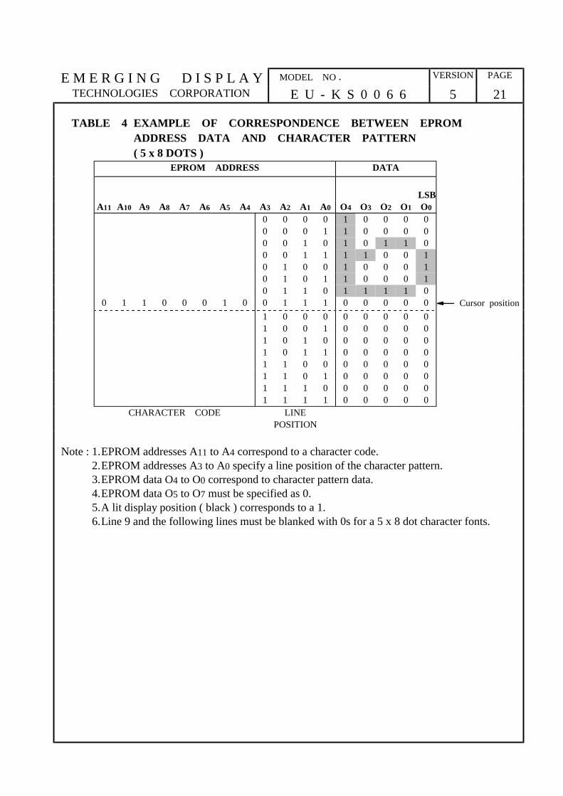
TABLE 4 EXAMPLE OF CORRESPONDENCE BETWEEN EPROM ADDRESS DATA AND CHARACTER PATTERN ( 5 x 8 DOTS )
EPROM ADDRESS DATA
LSB
A11 A10 A9 A8 A7 A6 A5 A4 A3 A2 A1 A0 O4 O3 O2 O1 O0
0 0 0 0 1 0 0 0 00 0 0 1 1 0 0 0 00 0 1 0 1 0 1 1 00 0 1 1 1 1 0 0 10 1 0 0 1 0 0 0 10 1 0 1 1 0 0 0 10 1 1 0 1 1 1 1 0
0 1 1 0 0 0 1 0 0 1 1 1 0 0 0 0 0 Cursor position
1 0 0 0 0 0 0 0 01 0 0 1 0 0 0 0 01 0 1 0 0 0 0 0 01 0 1 1 0 0 0 0 01 1 0 0 0 0 0 0 01 1 0 1 0 0 0 0 01 1 1 0 0 0 0 0 01 1 1 1 0 0 0 0 0
CHARACTER CODE LINEPOSITION
Note : 1.2.3.4.5.6.
EPROM addresses A11 to A4 correspond to a character code.EPROM addresses A3 to A0 specify a line position of the character pattern.EPROM data O4 to O0 correspond to character pattern data.EPROM data O5 to O7 must be specified as 0.A lit display position ( black ) corresponds to a 1.Line 9 and the following lines must be blanked with 0s for a 5 x 8 dot character fonts.

E M E R G I N G D I S P L A Y MODEL NO . VERSION PAGE
TECHNOLOGIES CORPORATION E U - K S 0 0 6 6 5 22
TABLE 5 EXAMPLE OF CORRESPONDENCE BETWEEN EPROM ADDRESS DATA AND CHARACTER PATTERN ( 5 x 10 DOTS )
EPROM ADDRESS DATA
LSBA11 A10 A9 A8 A7 A6 A5 A4 A3 A2 A1 A0 O4 O3 O2 O1 O0
0 0 0 0 0 0 0 0 00 0 0 1 0 0 0 0 00 0 1 0 0 1 1 0 10 0 1 1 1 0 0 1 10 1 0 0 1 0 0 0 10 1 0 1 1 0 0 0 10 1 1 0 0 1 1 1 1
0 1 0 1 0 0 1 0 0 1 1 1 0 0 0 0 11 0 0 0 0 0 0 0 11 0 0 1 0 0 0 0 11 0 1 0 0 0 0 0 0 Cursor position
1 0 1 1 0 0 0 0 01 1 0 0 0 0 0 0 01 1 0 1 0 0 0 0 01 1 1 0 0 0 0 0 01 1 1 1 0 0 0 0 0
CHARACTER CODE LINEPOSITION
Note: 1.2.3.4.5.6.
EPROM addresses A11 to A4 correspond to a character code.EPROM addresses A3 to A0 specify a line position of the character pattern.EPROM data O4 to O0 correspond to character pattern data.EPROM data O5 to O7 must be specified as 0.A lit display position ( black ) corresponds to a 1.Line 11 and the following lines must be blanked with 0s for a 5 x 10 dot characterfonts.
E M E R G I N G D I S P L A Y MODEL NO . VERSION PAGE
TECHNOLOGIES CORPORATION E U - K S 0 0 6 6 5 23
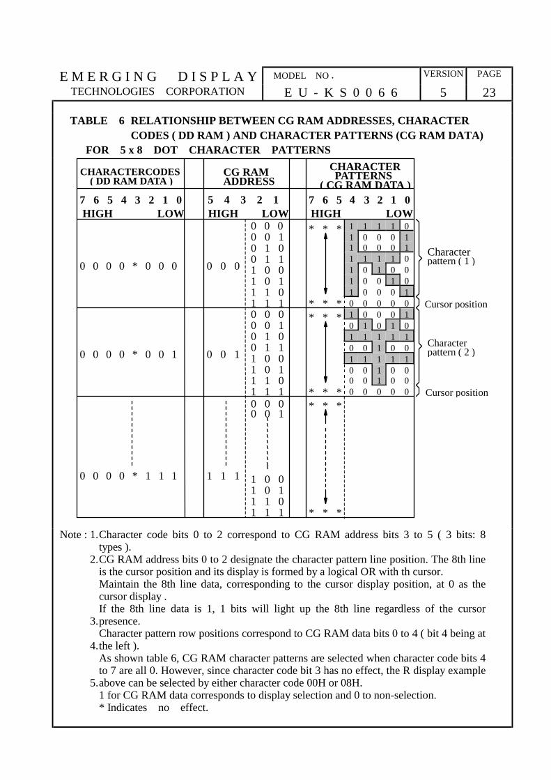
TABLE 6 RELATIONSHIP BETWEEN CG RAM ADDRESSES, CHARACTER CODES ( DD RAM ) AND CHARACTER PATTERNS (CG RAM DATA)
FOR 5 x 8 DOT CHARACTER PATTERNS
CHARACTERCODES ( DD RAM DATA )
CG RAMADDRESS
5 4 3 2 1
CHARACTERPATTERNS
( CG RAM DATA )
HIGH LOW HIGH LOW LOWHIGH0 0 00 0 10 1 00 1 11 0 01 0 11 1 01 1 1
* * *
* * *
0 0 0 0 * 0 0 0 0 0 0
0 0 10 0 0 0 * 0 0 1
* * *
* * *0 0 00 0 1
1 1 1 1 0 01 0 11 1 01 1 1
0 0 0 0 * 1 1 1
* * *
* * *
Characterpattern ( 1 )
Cursor position
Characterpattern ( 2 )
Cursor position
7 6 5 4 3 2 1 0 7 6 5 4 3 2 1 0
0 0 00 0 10 1 00 1 11 0 01 0 11 1 01 1 1
1 1 1 1 01 0 0 0 11 0 0 0 11 1 1 1 01 0 1 0 01 0 0 1 01 0 0 0 10 0 0 0 01 0 0 0 10 1 0 1 01 1 1 1 10 0 1 0 01 1 1 1 10 0 1 0 00 0 1 0 00 0 0 0 0
Note : 1.
2.
3.
4.
5.
Character code bits 0 to 2 correspond to CG RAM address bits 3 to 5 ( 3 bits: 8types ).CG RAM address bits 0 to 2 designate the character pattern line position. The 8th lineis the cursor position and its display is formed by a logical OR with th cursor.Maintain the 8th line data, corresponding to the cursor display position, at 0 as thecursor display .If the 8th line data is 1, 1 bits will light up the 8th line regardless of the cursorpresence.Character pattern row positions correspond to CG RAM data bits 0 to 4 ( bit 4 being atthe left ).As shown table 6, CG RAM character patterns are selected when character code bits 4to 7 are all 0. However, since character code bit 3 has no effect, the R display exampleabove can be selected by either character code 00H or 08H.1 for CG RAM data corresponds to display selection and 0 to non-selection.* Indicates no effect.
E M E R G I N G D I S P L A Y MODEL NO . VERSION PAGE
TECHNOLOGIES CORPORATION E U - K S 0 0 6 6 5 24
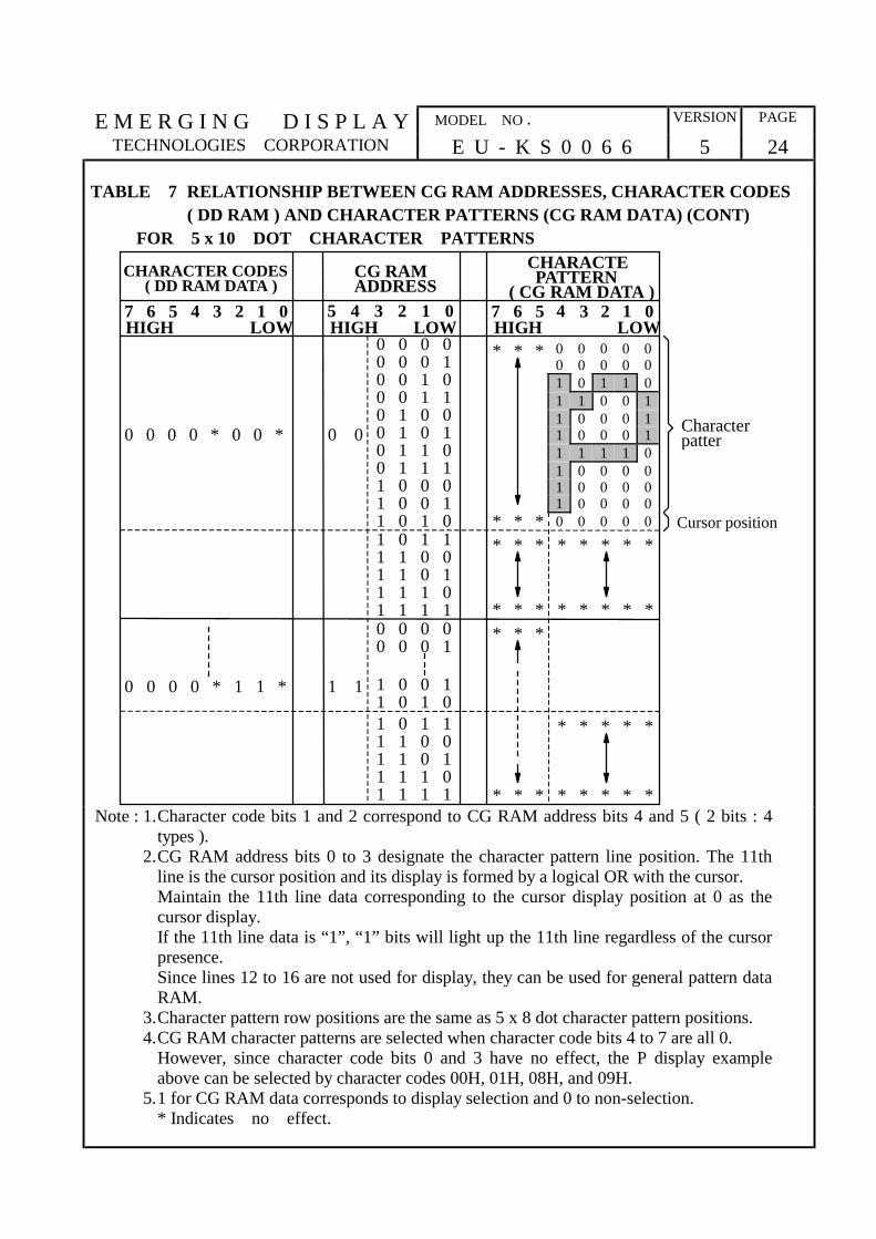
TABLE 7 RELATIONSHIP BETWEEN CG RAM ADDRESSES, CHARACTER CODES ( DD RAM ) AND CHARACTER PATTERNS (CG RAM DATA) (CONT)
FOR 5 x 10 DOT CHARACTER PATTERNS
CHARACTER CODES ( DD RAM DATA )
CG RAMADDRESS
5 4 3 2 1 0
CHARACTEPATTERN
( CG RAM DATA )
HIGH LOW HIGH LOW LOWHIGH0 0 0 00 0 0 10 0 1 00 0 1 10 1 0 00 1 0 10 1 1 00 1 1 1
* * *
* * *
0 0 0 0 * 0 0 * 0 0
* * *
* * *0 0 0 00 0 0 1
1 1 1 0 0 11 0 1 0
0 0 0 0 * 1 1 *
* * *
* * *
Characterpatter
Cursor position
7 6 5 4 3 2 1 0 7 6 5 4 3 2 1 0
1 0 0 01 0 0 11 0 1 01 0 1 11 1 0 01 1 0 11 1 1 01 1 1 1
1 0 1 11 1 0 01 1 0 11 1 1 01 1 1 1
* * * * *
* * * * *
* * * * *
* * * * *
0 0 0 0 00 0 0 0 01 0 1 1 01 1 0 0 11 0 0 0 11 0 0 0 11 1 1 1 01 0 0 0 01 0 0 0 01 0 0 0 00 0 0 0 0
Note : 1.
2.
3.4.
5.
Character code bits 1 and 2 correspond to CG RAM address bits 4 and 5 ( 2 bits : 4types ).CG RAM address bits 0 to 3 designate the character pattern line position. The 11thline is the cursor position and its display is formed by a logical OR with the cursor.Maintain the 11th line data corresponding to the cursor display position at 0 as thecursor display.If the 11th line data is “1”, “1” bits will light up the 11th line regardless of the cursorpresence.Since lines 12 to 16 are not used for display, they can be used for general pattern dataRAM.Character pattern row positions are the same as 5 x 8 dot character pattern positions.CG RAM character patterns are selected when character code bits 4 to 7 are all 0.However, since character code bits 0 and 3 have no effect, the P display exampleabove can be selected by character codes 00H, 01H, 08H, and 09H.1 for CG RAM data corresponds to display selection and 0 to non-selection.* Indicates no effect.
E M E R G I N G D I S P L A Y MODEL NO . VERSION PAGE
TECHNOLOGIES CORPORATION E U - K S 0 0 6 6 5 25
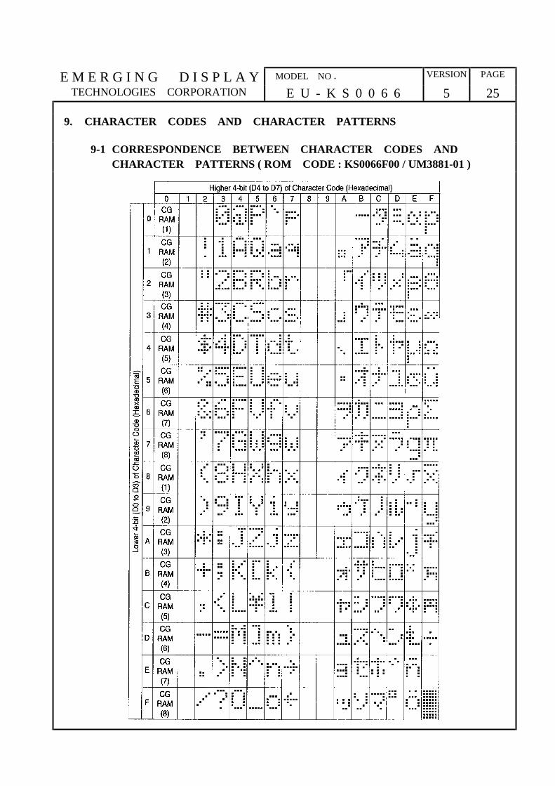
9. CHARACTER CODES AND CHARACTER PATTERNS
9-1 CORRESPONDENCE BETWEEN CHARACTER CODES AND CHARACTER PATTERNS ( ROM CODE : KS0066F00 / UM3881-01 )
E M E R G I N G D I S P L A Y MODEL NO . VERSION PAGE
TECHNOLOGIES CORPORATION E U - K S 0 0 6 6 5 26
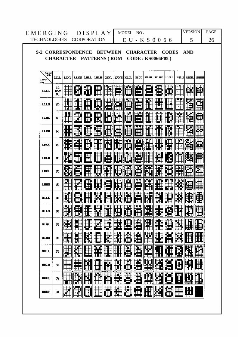
9-2 CORRESPONDENCE BETWEEN CHARACTER CODES AND CHARACTER PATTERNS ( ROM CODE : KS0066F05 )

E M E R G I N G D I S P L A Y MODEL NO . VERSION PAGE
TECHNOLOGIES CORPORATION E U - K S 0 0 6 6 5 27
9-3 CORRESPONDENCE BETWEEN CHARACTER CODES AND CHARACTER PATTERNS ( ROM CODE : UM3881-02 / SED1278D0B )

E M E R G I N G D I S P L A Y MODEL NO . VERSION PAGE
TECHNOLOGIES CORPORATION E U - K S 0 0 6 6 5 28
9-4 CORRESPONDENCE BETWEEN CHARACTER CODES AND CHARACTER PATTERNS ( ROM CODE : SED1278D0H )