Embed Size (px)
Citation preview

EMI Reduction in Discrete SMPS Using Programmable Gate Driver Output Resistance
by
Andrew William Shorten
A thesis submitted in conformity with the requirements for the degree of Master of Applied Science
Graduate Department of Electrical and Computer Engineering University of Toronto
© Copyright by Andrew William Shorten 2011

ii
EMI Reduction in SMPS Using Programmable Gate Driver Output
Resistance
Andrew Shorten
Master of Applied Science
Graduate Department of Electrical and Computer Engineering
University of Toronto
2011
Abstract
A gate driver IC with programmable driving strength to reduce electromagnetic interference (EMI) in
SMPS is presented in this thesis. The design builds on previous segmented gate driver designs that
have been used to improve light load efficiency. The presented solution is to dynamically adjust the
output resistance Rout at the arrival of each gate pulse to minimize EMI while maintaining low
switching loss. Dynamically adjusting Rout is not possible with conventional gate driver designs.
Thus, a segmented gate driver is designed and fabricated in the AMS 0.35μm 40V HVCMOS
process. Unlike traditional snubber circuits, the proposed method does not require extra discrete
components that dissipate energy. Experimental results indicate up to a 7dBμV improvement in peak
Conducted EMI (CEMI) between 20 MHz and 30 MHz and a 150μV/m improvement in peak
Radiated EMI (REMI) between 88 MHz and 216 MHz.

iii
Acknowledgments
First and foremost I would like to thank my research supervisor, Professor Wai Tung Ng. His
guidance and support throughout my degree has been very generous. His ability to understand
and interpret both the theoretical and applied aspects of electrical engineering research has been
invaluable. Furthermore, through his commitment to my academic development, I have been able
to attend four conferences during my Masters Degree, twice as a paper presenter. This
commitment has also been apparent in his willingness to include me in several trips to Japan for
talks with Fuji Electric. These trips have given me tremendous insight into the corporate as well
as the academic aspects of engineering research and development.
I would also like to thank my fellow graduate students and researchers, namely; Armin Akhvan
Fomani, Pearl Cao, April Zhao, Jing Wang, Sherrie Xie, Junmin Lee, Gang Xie and Masahiro
Sasaki. I will fondly remember your companionship and support during our shared time here at
the University of Toronto. In particular, I would like to thank Armin Akhavan Fomani, as his
research laid the foundation for much of the gate driver work I have accomplished during my
degree.
I would also like to thank Fuji Electric for its continuing support of our lab and my research.
Additionally, I would like to thank the Natural Science and Engineering Research Council and
the Canadian Microelectronics Corporation.
Finally, I would like to convey my most sincere gratitude to my many friends and family, their
support throughout my degree has been tremendous and very much appreciated. In particular, I
would like to express my heartfelt thanks to my girlfriend, Jessica Wu. She has put up with long
work days and frequent travelling, but has nevertheless continued to support and encourage me
and my work.

iv
Table of Contents
Acknowledgments ........................................................................................................................... ii
Table of Contents ........................................................................................................................... iv
List of Tables ................................................................................................................................ vii
List of Figures .............................................................................................................................. viii
Chapter 1 Introduction ............................................................................................................. 1
1.1 Discrete Low Voltage SMPS .............................................................................................. 1
1.2 EMI and EMC in SMPS ..................................................................................................... 2
1.3 Thesis Objective and Overview .......................................................................................... 2
Chapter 2 Background & Research Motivation ...................................................................... 4
2.1 The Synchronous Buck Converter ...................................................................................... 4
2.1.1 Basic Operation of the Synchronous Buck Converter ............................................ 4
2.1.2 The Synchronous Buck Converter and Dead Time ................................................ 8
2.2 Sources of Power Loss in Synchronous Buck Converters ................................................ 10
2.2.1 Switching Loss ...................................................................................................... 10
2.2.2 Gate Driver Loss ................................................................................................... 12
2.2.3 Gate Charge Loss .................................................................................................. 12
2.2.4 Conduction Loss ................................................................................................... 13
2.3 FCC Electromagnetic Interference Guidelines ................................................................. 14
2.3.1 Conducted EMI FCC Guidelines .......................................................................... 14
2.3.2 Radiated EMI FCC Guidelines ............................................................................. 15
2.4 Sources of EMI in the Buck Converter ............................................................................. 16
2.4.1 Current Switching ................................................................................................. 16
2.4.2 MOSFET Gate Node Ringing ............................................................................... 17

v
2.5 Typical EMI Reduction Techniques ................................................................................. 18
2.5.1 Input Filtering ....................................................................................................... 18
2.5.2 Snubber Circuits .................................................................................................... 19
2.5.3 Spread Spectrum Operation .................................................................................. 21
2.6 Typical Gate Driver Topologies ....................................................................................... 23
2.6.1 Voltage Driven Gate Drivers ................................................................................ 23
2.6.2 Current Driven Gate Drivers ................................................................................. 24
2.6.3 Resonance Driven Gate Drivers ............................................................................ 25
Chapter 3 Proposed EMI Reduction Technique .................................................................... 27
3.1 Effect of Rout on Switching Loss ..................................................................................... 27
3.2 The Effect of Rout on Electromagnetic Interference .......................................................... 28
3.3 Dynamic Rout Operation .................................................................................................... 30
3.4 Switching Characteristics .................................................................................................. 31
3.5 Gate Driver Topology ....................................................................................................... 32
3.6 Segment Design ................................................................................................................ 33
Chapter 4 Implementation and Experimental Results ........................................................... 34
4.1 IC Implementation ............................................................................................................ 34
4.2 Discrete System Implementation ...................................................................................... 35
4.3 Gating Signal Generation .................................................................................................. 40
4.4 Measurement of Conducted EMI and Efficiency ............................................................. 44
4.4.1 Measurement of Conducted EMI .......................................................................... 46
4.4.2 Measurement of Efficiency ................................................................................... 46
4.5 Measurement of Radiated EMI ......................................................................................... 47
4.6 Determining the Effects of Tpre and Tpost ........................................................................... 49
4.6.1 The Effects of the Tpre Variable ............................................................................ 49
4.6.2 The Effects of the Tpost Variable ........................................................................... 51

vi
4.7 Voltage Waveforms .......................................................................................................... 53
4.7.1 Voltage Waveform Measurement Strategy ........................................................... 53
4.7.2 Voltage Waveform Measurements ....................................................................... 54
4.8 Conducted EMI Spectrum and Efficiency Measurements ................................................ 57
4.9 Radiated EMI Measurements ............................................................................................ 60
Chapter 5 Conclusions and Future Work .............................................................................. 64
5.1 Thesis Summary ................................................................................................................ 64
5.2 Future Work ...................................................................................................................... 65
References ..................................................................................................................................... 66
Appendix A MOSFET Data Sheet ........................................................................................... 72

vii
List of Tables
Table 2.1 FCC Conducted EMI Guidelines .................................................................................. 14
Table 2.2 FCC Radiated EMI Guidelines ..................................................................................... 16
Table 4.1 Measured Gate Driver Output Resistance .................................................................... 35
Table 4.2 Operating Conditions for Testing ................................................................................. 45
Table 4.3 Converter Efficiency for Different Modes of Operation .............................................. 59

viii
List of Figures
Figure 2.1 Basic Synchronous Buck Converter Topology ............................................................. 4
Figure 2.2 CCM Switching Waveforms ......................................................................................... 5
Figure 2.3 DCM Switching Waveforms ......................................................................................... 6
Figure 2.4 Closed Loop Buck Converter ........................................................................................ 8
Figure 2.5 Dead Time Gating Example .......................................................................................... 9
Figure 2.6 Digitally Controlled Synchronous Buck Converter Topology .................................... 10
Figure 2.7 Voltage and Current Waveforms during MOSFET Turnoff ....................................... 11
Figure 2.8 FCC Conducted EMI Guidelines (Quasi Peak) ........................................................... 15
Figure 2.9 FCC Radiated EMI Guidelines .................................................................................... 16
Figure 2.10 Input Current Waveform, Ig, for CCM Operation ..................................................... 17
Figure 2.11 Gate Driver MOSFET RLC Circuit Formation ......................................................... 18
Figure 2.12 An Example of Input Filtering .................................................................................. 18
Figure 2.13 Input Current Waveform, Ig, With and Without Input Filtering ................................ 19
Figure 2.14 RLD Snubber Applied to Synchronous Buck Converter .......................................... 20
Figure 2.15 RCD Snubber Applied to Synchronous Buck Converter .......................................... 21
Figure 2.16 Averaged EMI spectrum of the input current to the DC-DC converter with fixed
frequency (Source: [35]) ............................................................................................................... 22
Figure 2.17 Averaged EMI spectrum of the input current to the DC-DC converter with the spread
spectrum enabled. (Source: [35]) .................................................................................................. 22

ix
Figure 2.18 Simplified Voltage Driven Gate Driver Topology .................................................... 23
Figure 2.19 Simplified Current Driven Gate Driver Topology .................................................... 24
Figure 2.20 Simplified Resonance Driven Gate Driver Topology ............................................... 25
Figure 2.21 Normalized Charge-Interval Current and Voltage waveforms for different resonant Q
values (Source: [36]) ..................................................................................................................... 26
Figure 3.1 Gate Driver RLC Circuit Formation ............................................................................ 28
Figure 3.2 Gate Driver IC Timing Diagram ................................................................................. 30
Figure 3.3 Proposed Gate Driver Topology .................................................................................. 32
Figure 3.4 Topology of an individual gate driver segment ........................................................... 33
Figure 4.1 Micrograph of Gate Driver IC ..................................................................................... 34
Figure 4.2 Synchronous Buck Converter System Schematic ....................................................... 36
Figure 4.3 Typical Voltage Controlled SMPS Topology ............................................................. 37
Figure 4.4 Open Loop SMPS Topology ....................................................................................... 37
Figure 4.5 Top and Bottom Layers of Synchronous Converter PCB Design ............................... 38
Figure 4.6 Synchronous Buck Converter PCB Implementation ................................................... 39
Figure 4.7 Counter Based DPWM Topology ............................................................................... 41
Figure 4.8 Delay Line Based DPWM Topology .......................................................................... 41
Figure 4.9 Hybrid DPWM Topology ............................................................................................ 42
Figure 4.10 Topology of the HCompare Module ......................................................................... 43
Figure 4.11 Modified Comparator Network ................................................................................. 44
Figure 4.12 Circuit Diagram of Experimental Test Setup ............................................................ 45
x
Figure 4.13 Radiated EMI Dipole Antenna Structure .................................................................. 47
Figure 4.14 Radiated EMI Test Setup (Side View) ...................................................................... 48
Figure 4.15 Radiated EMI Test Setup (Top View) ....................................................................... 48
Figure 4.16 Improvement in Conducted EMI VS Tpre ................................................................ 49
Figure 4.17 Converter Efficiency VS Tpre ................................................................................... 50
Figure 4.18 Improvement in Conducted EMI VS Tpost ............................................................... 51
Figure 4.19 Converter Efficiency VS Tpost ................................................................................. 52
Figure 4.20 Voltage Measurements For High Output Resistance (One Segment Enabled) ......... 55
Figure 4.21 Voltage Measurements For Low Output Resistance (All Segments Enabled) .......... 55
Figure 4.22 Voltage Measurements For Proposed Technique ...................................................... 56
Figure 4.23 Conducted EMI Spectrum for High Output Resistance (One Segment Enabled) ..... 58
Figure 4.24 Conducted EMI Spectrum for Low Output Resistance (All Segments Enabled) ..... 58
Figure 4.25 Conducted EMI Spectrum for Proposed Technique .................................................. 59
Figure 4.26 Ambient Radiated EMI Spectrum ............................................................................. 61
Figure 4.27 Radiated EMI Spectrum for Low Output Resistance (All Segments Enabled)......... 61
Figure 4.28 Radiated EMI Spectrum for High Output Resistance (One Segment Enabled) ........ 62
Figure 4.29 Radiated EMI Spectrum for Proposed Technique ..................................................... 62

1
Chapter 1 Introduction
As discrete Switch Mode Power Supplies (SMPS) are being operated at higher frequencies, the
need to reduce electromagnetic interference (EMI) is becoming critical [1]. This need arises as
the maximum EMI guidelines set forth by organizations such as the American Federal
Communications Commission (FCC) and the European Comité International Spécial des
Perturbations Radioélectriques (CISPR), must be strictly adhered to by commercial electronics
[2]. Furthermore, EMI can interfere with the operation of circuits connected to or nearby the
SMPS, causing them to malfunction [3]. Nevertheless, EMI mitigation is ideally carried out
without decreasing the efficiency or increasing the size or weight of the SMPS.
1.1 Discrete Low Voltage SMPS
Switch mode power supplies built using discrete components are an essential subsystem of
modern commercial electronics. Not only do SMPS provide systems with a high efficiency
method of converting electrical energy from one voltage level to another, they are also highly
flexible and allow the designer of the system a great deal of design freedom. This freedom arises
as the designer is free to mix and match discrete components as they wish in order to optimize
the converter for their specific application. These optimizations may take the form of conversion
ratio, load current, weight, size and even its monetary cost.
However, this flexibility does come at an expense as discrete SMPS systems cannot be switched
as quickly as their integrated counterparts [4]. This limitation means that in order to meet output
voltage ripple requirements, the passive components of the converter must be made larger [5],
subsequently increasing the size, weight and cost of the converter. Furthermore, some SMPS
enhancement techniques are unavailable to the discrete designer, such as segmentation of the
output stage in order to increase light load efficiency.

2
1.2 EMI and EMC in SMPS
A recent trend for SMPS design is to increase the switching frequency in order to reduce the
passive component size and subsequently increase energy density [6]. However, a result of this
trend (and the use of SMPS in general) is that the EMI generated by these systems has become a
serious problem [7]. Increased EMI degrades the electromagnetic compatibility (EMC) of
devices connected to or operating close to the SMPS. In other words, the EMI generated by
SMPS can render nearby devices inoperable. There are two forms of EMI that SMPS generate;
conducted EMI and radiated EMI [8].
Conducted EMI is emitted by SMPS as they draw current periodically at the switching frequency
from the input power source [27]. This periodic current draw causes both voltage and current
distortion in other devices connected to the same power source. A fundamental characteristic of
this distortion are the harmonics; much of the interference occurs at frequencies well above the
switching frequency [27]. Furthermore, ringing at nodes within the SMPS can also develop into
conducted EMI [9]. The FCC conducted EMI standards are defined between 150 kHz and 30
MHz [10].
Radiated EMI occurs when the SMPS generates radio waves that are emitted outward in all
directions by the circuit. Radiated EMI is particularly difficult to mitigate as it can cause
circuitry simply located near the SMPS to malfunction even if it is not physically connected to
the SMPS in any way. The same negative effects of conducted EMI exist for radiated EMI.
However, radiated EMI has the potential for severe impact on radio systems [11]. The FCC
radiated EMI standards are defined for frequencies above 30MHz.
As the control circuitry of the SMPS is often directly connected to the same supply, EMI can
cause malfunctions to occur in this circuitry as well. Thus, an SMPS that exhibits excessive EMI
can actually cause itself to malfunction [12]. The impact of EMI can be particularly worrisome to
system designers when the SMPS is to be used in mission critical applications such as medical or
aerospace equipment.
1.3 Thesis Objective and Overview
The objective of this work is to reduce EMI in a synchronous buck converter without reducing
efficiency and without the other penalties associated with traditional EMI reduction techniques.
3
In particular, this work will focus on whether or not a segmented voltage driven gate driver can
be employed to reduce both conducted and radiated EMI. This work is important as conducted
EMI can cause unwanted operation of devices connected to SMPS. Furthermore, many of the
established EMI reduction techniques degrade the benefits of using an SMPS in the first place,
such as reduced physical size and high conversion efficiency.
In order to accomplish the goal of this thesis, a segmented gate driver IC is fabricated and
incorporated into a discrete buck converter system. A novel technique for operating the
segmented gate driver IC is developed and experimental results are performed in order to verify
that the technique reduces EMI while ensuring that efficiency is not reduced.
This thesis is organized as follows; Chapter 2 reviews the required background information,
Chapter 3 discusses the proposed EMI reduction technique and the segmented gate driver design,
Chapter 4 reviews the physical implementation and experimental results. Finally, conclusions
and future work are discussed in Chapter 5.
4
Chapter 2 Background & Research Motivation
The basic operating principles and existing EMI suppression techniques are discussed in this
chapter.
2.1 The Synchronous Buck Converter
One of the most common forms of SMPS is the synchronous buck converter. Synchronous buck
converters are used to convert DC electrical power to a lower DC voltage level [13]. Power
conversion efficiencies above 90% can be practically realized with this topology [14]. An
example of the basic synchronous buck converter is shown in Figure 2.1.
2.1.1 Basic Operation of the Synchronous Buck Converter
The buck converter operates by repeatedly connecting the switching node (Vx) to either the input
power source (Vg) or ground using switches M1 and M2. The result of this operation is that a
square wave is formed at the switching node of the converter.
Vg
L
C
Control
Signal
Generator
M1
M2
Vx Vout
Figure 2.1 Basic Synchronous Buck Converter Topology

5
The operation of the converter is strongly related to the characteristics of this switching node
square wave. During continuous conduction mode (CCM), the converter is operated such that the
waveforms shown in Figure 2.2 are realized [15]. During CCM, the output voltage of the
converter is shown to be related to the duty cycle of the switching node voltage by (2.1) [15].
Time [s]
Time [s]
Time [s]
Time [s]
Time [s]
VM
1 [V
]V
M2
[V]
Vx
[V]
IL [A
]V
OU
T [V
]
DxTs DxTs(1-D)xTs (1-D)xTs
VON
VOFF
VON
VOFF
VG
IOUT
Figure 2.2 CCM Switching Waveforms

6
However, CCM only occurs when the current flowing through inductor L does not become zero.
If a zero inductor current does occur during the operation of the converter, the converter is said
to be operating in discontinuous conduction mode (DCM) [16]. During DCM, the converter is
operated such that the waveforms in Figure 2.3 are realized [16]. During DCM, the output
voltage is shown to be related to duty cycle of the switching node voltage by (2.2) [16].
Time [s]
Time [s]
Time [s]
Time [s]
Time [s]
VM
1 [V
]V
M2
[V]
Vx
[V]
IL [A
]V
OU
T [V
]
D1xTs
VON
VOFF
VON
VOFF
VG
IOUT
D2xTs D3xTs D1xTs D2xTs D3xTs
Figure 2.3 DCM Switching Waveforms

7
(2.1)
√ ,
(2.2)
While (2.1) and (2.2) are first order approximations of the behavior of the buck converter, they
are accurate enough that they can be used for practical control of the converter. The work in this
thesis focuses on the behavior of the converter during CCM. During CCM, the transfer function
of the converter from duty cycle input to the output voltage can be approximated by (2.3) [17].
Since (2.3) is a linear transfer function, the output voltage of the converter can be controlled
using traditional, closed loop control system techniques [17]. Accurate control of the output
voltage is an important requirement of many applications. Furthermore, (2.1) does not consider
the effect of changing load current, temperature and age. These unconsidered factors may distort
the output voltage but they can be corrected for using a closed loop feedback system. An
example of a typical closed loop control system for the buck converter is shown below in Figure
2.4. The system shown uses a feedback loop composed of voltage divider, a PID controller and a
pulse width modulator.
( )
(
)
(2.3)
√
√

8
Vg
L
C
PWM
Generator
M1
M2
Vx Vout
PID ControllerDuty Cycle Command
R1
R2
Sensed Voltage
R
Figure 2.4 Closed Loop Buck Converter
2.1.2 The Synchronous Buck Converter and Dead Time
The basic operation of the buck converter discussed in in Section 2.1.1 reveals a potential
problem with the power switches. As Figure 2.2 and Figure 2.3 show, switches M1 and M2 are
enabled and disabled in a successive, recurring manner. This operation theoretically works well
as only one of the switches should be enabled at any given time. However, power semiconductor
switches cannot turn on and off instantaneously. This fact results in a potential situation where
one switch is activated before the other one has been given sufficient time to turn off. If this
situation occurs, power source Vg will be shorted to ground through switches M1 and M2, a
phenomenon known as cross conduction [18]. This is a highly undesirable occurrence as it
wastes energy and could destroy the converter.
9
Nevertheless, there is an established method for mitigating cross conduction current. This
method is achieved by introducing what is known as dead-time into the gating signals of the
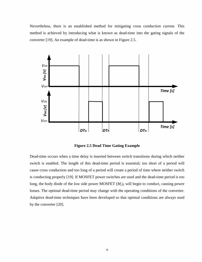
converter [19]. An example of dead-time is as shown in Figure 2.5.
Time [s]
Time [s]
VM
1 [V
]V
M2
[V]
VON
VOFF
VON
VOFF
DTN DTNDTP
Figure 2.5 Dead Time Gating Example
Dead-time occurs when a time delay is inserted between switch transitions during which neither
switch is enabled. The length of this dead-time period is essential; too short of a period will
cause cross conduction and too long of a period will create a period of time where neither switch
is conducting properly [19]. If MOSFET power switches are used and the dead-time period is too
long, the body diode of the low side power MOSFET (M2), will begin to conduct, causing power
losses. The optimal dead-time period may change with the operating conditions of the converter.
Adaptive dead-time techniques have been developed so that optimal conditions are always used
by the converter [20].

10
2.2 Sources of Power Loss in Synchronous Buck Converters
The synchronous buck converter exhibits different power losses; these include switching loss,
gate driver loss, gate charge loss and conduction loss.
Vg
L
C
Digital
Controller
M1
M2
VoutHS Gate Driver
LS Gate Driver
Figure 2.6 Digitally Controlled Synchronous Buck Converter Topology
2.2.1 Switching Loss
Like all power MOSFETs, the high-side and low-side MOSFET switches (M1 and M2
respectively) do not switch on and off instantaneously. The result of this non-zero switching time
is that for every cycle, there is an instantaneous power loss associated with every switch known
as switching loss [21]. When a MOSFET switch is observed while it turns off, it can be easily
seen how switching loss occurs. In this case, switching loss occurs because current does not
immediately cease to flow through the switch as it turns off. Thus, as the forward blocking
voltage of the switch begins to increase, current is still flowing through the device, causing
power loss. An example of the voltage and current waveforms for M1 during turn-off as well as
the instantaneous power loss during the transition are shown in Figure 2.7.

11
Time [s]
Time [s]
VD
S (
t) a
nd I
DS (
t)P
(t)
= V
DS (
t) x
ID
S (
t)
IDS(t)
VDS(t)
Toff
Figure 2.7 Voltage and Current Waveforms during MOSFET Turnoff
From Figure 2.7 it can be seen that the switching loss can be expressed as (2.4) where fsw is the
switching frequency, VDS is the drain to source voltage that is blocked in the off state, IL is the
load current and TON and TOFF are the turn on and turn off times, respectively. From (2.4) it can
be seen that the switching loss scales linearly with both switching frequency and the transition
times of the switches. This observation is particularly relevant as there is currently a trend to
increase the switching frequency of SMPS in order to reduce passive component size.
Furthermore, from (2.4) it can be seen that switching loss can be mitigated by ensuring fast
transition times for the MOSFET switches.
(
)
(2.4)
12
2.2.2 Gate Driver Loss
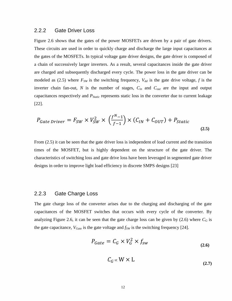
Figure 2.6 shows that the gates of the power MOSFETs are driven by a pair of gate drivers.
These circuits are used in order to quickly charge and discharge the large input capacitances at
the gates of the MOSFETs. In typical voltage gate driver designs, the gate driver is composed of
a chain of successively larger inverters. As a result, several capacitances inside the gate driver
are charged and subsequently discharged every cycle. The power loss in the gate driver can be
modeled as (2.5) where FSW is the switching frequency, Vdd is the gate drive voltage, f is the
inverter chain fan-out, N is the number of stages, Cin and Cout are the input and output
capacitances respectively and PStatic represents static loss in the converter due to current leakage
[22].
(
) ( )
(2.5)
From (2.5) it can be seen that the gate driver loss is independent of load current and the transition
times of the MOSFET, but is highly dependent on the structure of the gate driver. The
characteristics of switching loss and gate drive loss have been leveraged in segmented gate driver
designs in order to improve light load efficiency in discrete SMPS designs [23]
2.2.3 Gate Charge Loss
The gate charge loss of the converter arises due to the charging and discharging of the gate
capacitances of the MOSFET switches that occurs with every cycle of the converter. By
analyzing Figure 2.6, it can be seen that the gate charge loss can be given by (2.6) where CG is
the gate capacitance, VGate is the gate voltage and fSW is the switching frequency [24].
(2.6)
(2.7)

13
From (2.6) and (2.7) it can be seen that gate charge loss is proportional to the width of the gate
MOSFET, W, for a given feature size L.
2.2.4 Conduction Loss
The conduction loss of the converter arises due to parasitic resistances that are found in the
converter. A common example of conduction loss is the on-resistance of the MOSFET switches
[25]. Analyzing Figure 2.6 shows that the conduction loss due to the on-resistance in the
MOSFET switches is given by (2.8) where IL is the load current and RON is the on-resistance of
the MOSFETs (assuming the high side and low side MOSFETs are identical).
(2.8)
(2.9)
Equations (2.8) and (2.9) show that the conduction loss is inversely proportional to the width of
the gate MOSFET, W, for a given feature size L. Thus, there is a tradeoff between the gate
charge loss and the conduction loss of the converter. This tradeoff is leveraged in segmented
output stage designs in order to improve light load efficiency in integrated SMPS designs.

14
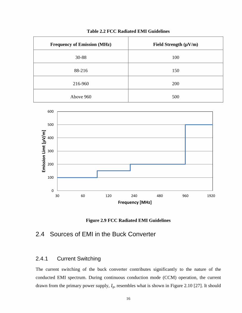
2.3 FCC Electromagnetic Interference Guidelines
2.3.1 Conducted EMI FCC Guidelines
The FCC guidelines for conducted emissions are discussed in section 15.107 of the FCC
standards [26]. In particular, these are the emission limits for non Class-A digital devices.
These guidelines consist of the maximum emission levels that are allowed to be conducted by a
device. The maximum allowed level is highly dependent on the frequency of the emission.
Table 2.1 shows these maximums and Figure 2.8 shows a graphical representation of them. The
conducted EMI guidelines are only defined between 150 kHz and 30 MHz. Above 30 MHz, the
emission guidelines are only defined for radiated emissions, which are described below in
Section 2.3.2. No guidelines are defined for any emissions below 150 kHz. As there are no
conducted emission guidelines set forth by the FCC for frequencies above 30 MHz and below
150 kHz, the work in this thesis only examines the impact on conducted emissions between 150
kHz and 30 MHz.
Table 2.1 FCC Conducted EMI Guidelines
Frequency of Emissions (MHz)
Conducted Limits (dBµV)
Quasi-Peak Average
0.15-5 66-56* 56-46*
0.5-5 56 46
5-30 60 50
*Decreases with the logarithm of frequency

15
Figure 2.8 FCC Conducted EMI Guidelines (Quasi Peak)
2.3.2 Radiated EMI FCC Guidelines
The FCC guidelines for radiated emissions are discussed in section 15.109 of the FCC standards
[26]. These guidelines consist of the maximum measured values of radiated emissions that can
be detected at various frequencies. Table 2.2 shows these maximums and Figure 2.9 shows a
graphical representation of them. The conducted EMI guidelines are only defined above 30
MHz. Thus the work presented in this thesis only focuses on the impact of the proposed
technique on radiated emissions above 30 MHz.
54
56
58
60
62
64
66
68
0.15 0.3 0.6 1.2 2.4 4.8 9.6 19.2
Emis
sio
n L
imt
[dB
µV
]
Frequency [MHz]
16
Table 2.2 FCC Radiated EMI Guidelines
Frequency of Emission (MHz) Field Strength (µV/m)
30-88 100
88-216 150
216-960 200
Above 960 500
Figure 2.9 FCC Radiated EMI Guidelines
2.4 Sources of EMI in the Buck Converter
2.4.1 Current Switching
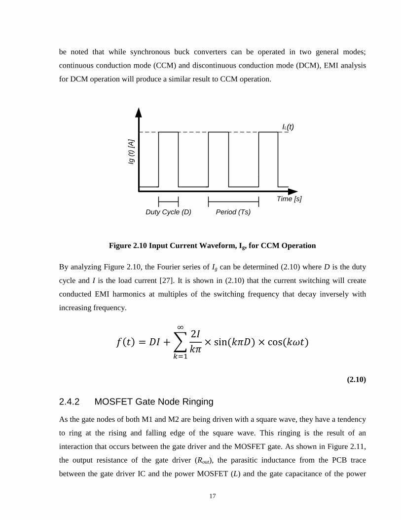
The current switching of the buck converter contributes significantly to the nature of the
conducted EMI spectrum. During continuous conduction mode (CCM) operation, the current
drawn from the primary power supply, Ig, resembles what is shown in Figure 2.10 [27]. It should
0
100
200
300
400
500
600
30 60 120 240 480 960 1920
Emis
sio
n L
imt
[µV
/m]
Frequency [MHz]
17
be noted that while synchronous buck converters can be operated in two general modes;
continuous conduction mode (CCM) and discontinuous conduction mode (DCM), EMI analysis
for DCM operation will produce a similar result to CCM operation.
Time [s]
Ig (
t) [
A]
IL(t)
Duty Cycle (D) Period (Ts)
Figure 2.10 Input Current Waveform, Ig, for CCM Operation
By analyzing Figure 2.10, the Fourier series of Ig can be determined (2.10) where D is the duty
cycle and I is the load current [27]. It is shown in (2.10) that the current switching will create
conducted EMI harmonics at multiples of the switching frequency that decay inversely with
increasing frequency.
( ) ∑
( ) ( )
(2.10)
2.4.2 MOSFET Gate Node Ringing
As the gate nodes of both M1 and M2 are being driven with a square wave, they have a tendency
to ring at the rising and falling edge of the square wave. This ringing is the result of an
interaction that occurs between the gate driver and the MOSFET gate. As shown in Figure 2.11,
the output resistance of the gate driver (Rout), the parasitic inductance from the PCB trace
between the gate driver IC and the power MOSFET (L) and the gate capacitance of the power
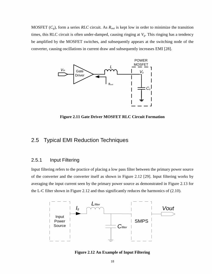
18
MOSFET (Cg), form a series RLC circuit. As Rout is kept low in order to minimize the transition
times, this RLC circuit is often under-damped, causing ringing at Vg. This ringing has a tendency
be amplified by the MOSFET switches, and subsequently appears at the switching node of the
converter, causing oscillations in current draw and subsequently increases EMI [28].
Figure 2.11 Gate Driver MOSFET RLC Circuit Formation
2.5 Typical EMI Reduction Techniques
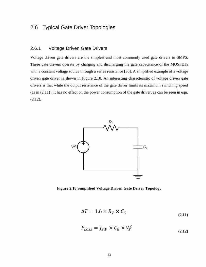
2.5.1 Input Filtering
Input filtering refers to the practice of placing a low pass filter between the primary power source
of the converter and the converter itself as shown in Figure 2.12 [29]. Input filtering works by
averaging the input current seen by the primary power source as demonstrated in Figure 2.13 for
the L-C filter shown in Figure 2.12 and thus significantly reduces the harmonics of (2.10).
Input
Power
Source
Lfilter
SMPS
VoutIg
Cfilter
Figure 2.12 An Example of Input Filtering
Gate
Driver
L
Cg
Vg
Rout
Vin
POWER
MOSFET

19
While input filters are effective at eliminating conducted EMI they have two major drawbacks.
First, the presence of an inductive circuit between the primary power source and converter
changes the transfer characteristics of the power converter, making the converter more difficult
to control [30]. Secondly, effective input filtering can require large passive components,
increasing the size, weight and cost of the converter.
Time [s]
Ig (
t) [A
]
Duty Cycle (D) Period (Ts)
Without
Filtering
With
Filtering
Figure 2.13 Input Current Waveform, Ig, With and Without Input Filtering
2.5.2 Snubber Circuits
Snubber circuits are often added to SMPS in order to reduce EMI. Snubbers operate by either
dampening or clamping the current or voltage found at a particular node, eliminating the ringing,
overshoot and undershoot that cause EMI [31]. A pair of snubber circuits that are commonly
used to reduce EMI in buck converters is the RLD and RCD snubbers [32]. Examples of the
RLD and RCD snubbers and how they are applied to the buck converter are shown in Figure
2.14 and Figure 2.15, respectively.

20
While snubber circuits are quite effective at eliminating EMI, they are commonly dissipative in
nature [33]. In other words, they either absorb energy from the circuit or they slow down the
transition times, ultimately increasing switching loss. Furthermore, snubbers require extra
passive components; increasing the size, weight and cost of the converter in a similar manner to
input filtering.
Vg
L
C
Digital
Controller
M1
M2
VoutHS Gate Driver
LS Gate Driver
Lsnub
Rsnub
DsnubRL
D S
nu
bb
er
Figure 2.14 RLD Snubber Applied to Synchronous Buck Converter

21
Vg
L
C
Digital
Controller
M1
M2
Vout
HS Gate Driver
LS Gate Driver
RC
D S
nu
bb
er
Rsnub Dsnub
Csnub
Figure 2.15 RCD Snubber Applied to Synchronous Buck Converter
2.5.3 Spread Spectrum Operation
Spread spectrum operation reduces EMI by taking the harmonics that results from the switching
frequency of the converter and distributing them over a wide range of frequencies instead of
concentrating them at the clock frequency and its harmonic multiples [34]. This behavior is
achieved by dynamically varying the switching frequency of the converter in real time. An
example of the impact of spread spectrum operation on conducted EMI is shown in Figure 2.16
and Figure 2.17.

22
Figure 2.16 Averaged EMI spectrum of the input current to the DC-DC converter with
fixed frequency (Source: [35])
Figure 2.17 Averaged EMI spectrum of the input current to the DC-DC converter with the
spread spectrum enabled. (Source: [35])
Spread spectrum operation lends itself better to integrated designs, where the custom analog and
digital components required for a changing clock frequency can be easily and compactly
implemented. Furthermore, the clock frequency of the converter cannot be spread over too large
a range as the efficiency and ripple performance of the converter may begin to be affected. Also,
with a digital PID controller, the location of the poles and zeroes are dependent on the clock
frequency, thus with spread spectrum operation, the controllers behavior could become
unpredictable [34].
23
2.6 Typical Gate Driver Topologies
2.6.1 Voltage Driven Gate Drivers
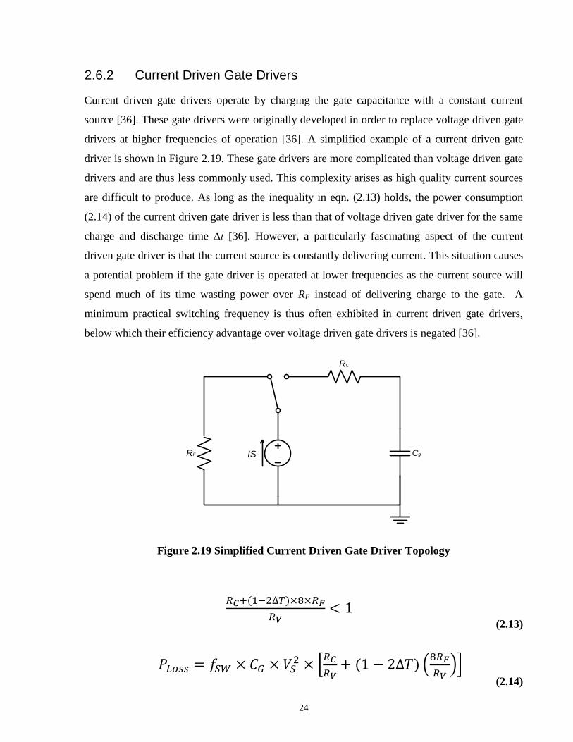
Voltage driven gate drivers are the simplest and most commonly used gate drivers in SMPS.
These gate drivers operate by charging and discharging the gate capacitance of the MOSFETs
with a constant voltage source through a series resistance [36]. A simplified example of a voltage
driven gate driver is shown in Figure 2.18. An interesting characteristic of voltage driven gate
drivers is that while the output resistance of the gate driver limits its maximum switching speed
(as in (2.11)), it has no effect on the power consumption of the gate driver, as can be seen in eqn.
(2.12).
VS
RV
Cg
Figure 2.18 Simplified Voltage Driven Gate Driver Topology
(2.11)
(2.12)
24
2.6.2 Current Driven Gate Drivers
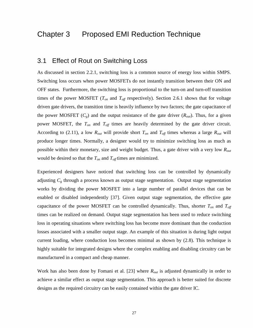
Current driven gate drivers operate by charging the gate capacitance with a constant current
source [36]. These gate drivers were originally developed in order to replace voltage driven gate
drivers at higher frequencies of operation [36]. A simplified example of a current driven gate
driver is shown in Figure 2.19. These gate drivers are more complicated than voltage driven gate
drivers and are thus less commonly used. This complexity arises as high quality current sources
are difficult to produce. As long as the inequality in eqn. (2.13) holds, the power consumption
(2.14) of the current driven gate driver is less than that of voltage driven gate driver for the same
charge and discharge time ∆t [36]. However, a particularly fascinating aspect of the current
driven gate driver is that the current source is constantly delivering current. This situation causes
a potential problem if the gate driver is operated at lower frequencies as the current source will
spend much of its time wasting power over RF instead of delivering charge to the gate. A
minimum practical switching frequency is thus often exhibited in current driven gate drivers,
below which their efficiency advantage over voltage driven gate drivers is negated [36].
IS
RC
CgRF
Figure 2.19 Simplified Current Driven Gate Driver Topology
( )
(2.13)
*
( ) (
)+
(2.14)

25
2.6.3 Resonance Driven Gate Drivers
Resonance driven gate drivers operate by transferring energy from an inductor into the gate
capacitance [36]. A simplified example of a resonance driven gate driver is shown in Figure
2.20. Clamped resonance occurs when the diode Dclamp and resistor Rp are added to the circuit,
full resonance occurs when these circuit elements are removed. In clamped resonance, the charge
time of the gate driver is dictated by the Q factor of the circuit (2.15) as shown in Figure 2.21,
but the gate voltage is clamped to voltage VS. In full resonance, both the turn on time and the
final gate voltage are determined by the Q factor.
VS
RR
Cg
LR
DclampRP
Figure 2.20 Simplified Resonance Driven Gate Driver Topology
√ ⁄
(2.15)
An advantage of the resonance driven gate driver is that energy can be recovered from the
circuit, eliminating some loss. However, this comes at the expense of several discrete
components that must be added to the system, increasing the weight and cost.

26
Figure 2.21 Normalized Charge-Interval Current and Voltage waveforms for different
resonant Q values (Source: [36])
Chapter 2 has discussed the basic buck converter topology, the fundamentals of EMI, existing
EMI suppression methods and basic power MOSFET gate driver topologies. Chapter 3 discusses
the proposed technique of the thesis. This technique utilizes a segmented voltage driven gate
driver in order to reduce the EMI emitted by SMPS.
27
Chapter 3 Proposed EMI Reduction Technique
3.1 Effect of Rout on Switching Loss
As discussed in section 2.2.1, switching loss is a common source of energy loss within SMPS.
Switching loss occurs when power MOSFETs do not instantly transition between their ON and
OFF states. Furthermore, the switching loss is proportional to the turn-on and turn-off transition
times of the power MOSFET (Ton and Toff respectively). Section 2.6.1 shows that for voltage
driven gate drivers, the transition time is heavily influence by two factors; the gate capacitance of
the power MOSFET (Cg) and the output resistance of the gate driver (Rout). Thus, for a given
power MOSFET, the Ton and Toff times are heavily determined by the gate driver circuit.
According to (2.11), a low Rout will provide short Ton and Toff times whereas a large Rout will
produce longer times. Normally, a designer would try to minimize switching loss as much as
possible within their monetary, size and weight budget. Thus, a gate driver with a very low Rout
would be desired so that the Ton and Toff times are minimized.
Experienced designers have noticed that switching loss can be controlled by dynamically
adjusting Cg through a process known as output stage segmentation. Output stage segmentation
works by dividing the power MOSFET into a large number of parallel devices that can be
enabled or disabled independently [37]. Given output stage segmentation, the effective gate
capacitance of the power MOSFET can be controlled dynamically. Thus, shorter Ton and Toff
times can be realized on demand. Output stage segmentation has been used to reduce switching
loss in operating situations where switching loss has become more dominant than the conduction
losses associated with a smaller output stage. An example of this situation is during light output
current loading, where conduction loss becomes minimal as shown by (2.8). This technique is
highly suitable for integrated designs where the complex enabling and disabling circuitry can be
manufactured in a compact and cheap manner.
Work has also been done by Fomani et al. [23] where Rout is adjusted dynamically in order to
achieve a similar effect as output stage segmentation. This approach is better suited for discrete
designs as the required circuitry can be easily contained within the gate driver IC.
28
3.2 The Effect of Rout on Electromagnetic Interference
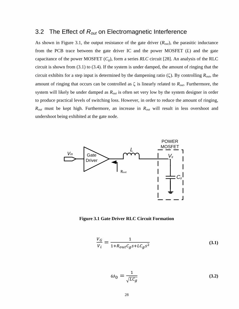
As shown in Figure 3.1, the output resistance of the gate driver (Rout), the parasitic inductance
from the PCB trace between the gate driver IC and the power MOSFET (L) and the gate
capacitance of the power MOSFET (Cg), form a series RLC circuit [28]. An analysis of the RLC
circuit is shown from (3.1) to (3.4). If the system is under damped, the amount of ringing that the
circuit exhibits for a step input is determined by the dampening ratio (). By controlling Rout, the
amount of ringing that occurs can be controlled as is linearly related to Rout. Furthermore, the
system will likely be under damped as Rout is often set very low by the system designer in order
to produce practical levels of switching loss. However, in order to reduce the amount of ringing,
Rout must be kept high. Furthermore, an increase in Rout will result in less overshoot and
undershoot being exhibited at the gate node.
Figure 3.1 Gate Driver RLC Circuit Formation
(3.1)
√ (3.2)
Gate
Driver
L
Cg
Vg
Rout
Vin
POWER
MOSFET

29
√
(3.3)
√
L
CR gout
2
(3.4)
Reducing ringing at the gate nodes of power MOSFETSs is important as ringing at these nodes
may result in oscillations in the current drawn by the converter, subsequently producing EMI.
The reason that this phenomenon could occur is that during the transition of the power MOSFET,
the device will spend a small amount of time in saturation mode and will behave as a voltage
controlled current source. Thus, any oscillations in voltage at the gate of the power MOSFET
will be translated into oscillations in current that are injected directly into the input power supply
of the SMPS.

30
3.3 Dynamic Rout Operation
The observation in sections 3.1 and 3.2 suggest that there is a tradeoff between EMI generated by
an SMPS and the efficiency of the overall converter. Looking at the mechanisms behind this
tradeoff indicates that the output resistance of the gate driver, Rout, plays an important role. A low
value for Rout provides a low amount of switching loss for the converter and thus improves
efficiency. However, a high value for Rout will reduce EMI. Essentially, a low value of Rout
provides short switching times but encourages ringing whereas a high Rout provides long
switching times but reduces ringing. As traditional voltage driven gate drivers have a static Rout,
a system designer is constrained by this tradeoff. They must pick a gate driver for their system
that sufficiently inhibits switching loss but at the same time does not encourage excessive
ringing.
The work presented in this thesis seeks to break this EMI-efficiency tradeoff and provide the
designer with a new design tool. In order to perform this task, a new voltage driven gate driver is
presented. In this structure, the output resistance, Rout is not static but instead can be adjusted
dynamically. With this approach, the gate drive can be operated in the manner shown in Figure
3.2.
Figure 3.2 Gate Driver IC Timing Diagram
31
With this operation, the output resistance of the gate driver is held low during output transitions
but is held high after the transition has passed. Through this operation, a short transition time is
guaranteed but any oscillations of the gate node that follow the transitions will be damped by the
higher output resistance of the gate driver. Thus, the tradeoff between EMI and efficiency can be
broken at the expense of a more complex gate driver circuit.
At first glance, it could be easily surmised that in order to maximize the benefits of this approach
the ideal maximum Rout value and the ideal minimum Rout resistance value (Routh and Routl
respectively) would be infinite and zero respectively. There are however reasons why this
arrangement is not possible. Firstly, it would be impossible to produce a practical device with a
zero value for Routl; all known room temperature materials exhibit non-zero electrical resistance.
A gate driver with a very large Routh value that is effectively infinite is possible to construct.
However, any leakage current at the gate of the MOSFET would steadily discharge the gate,
causing significant conduction losses in the MOSFET. Thus, Routh must be selected to be a finite
value.
3.4 Switching Characteristics
The proposed switching waveform shown in Figure 3.2 uses two variables to define the
operation of the gate driver; Tpost and Tpre. Tpost is defined as the time after the transition that Rout
remains low. Tpre is defined as the time before the transition that Rout becomes low. This
characterization has been used as a simplified approach and does not incorporate the possibility
of using more than two values for Rout. Additionally, the same Tpost and Tpre values are used for
both the rising and falling edges of the gate driver pulse. Nevertheless, despite these
simplifications, the characterization does provide enough control over the system in order to
explore the behavior of the proposed technique.
Tpost and Tpre must be selected such that they break the tradeoff between switching loss and EMI
while at the same time not interfering with the normal operation of the converter. Furthermore,
the values are only specific to a particular converter design. Changing the MOSFETs used in the
SMPS or voltage levels of the system will likely require new values for Tpost and Tpre.

32
3.5 Gate Driver Topology
In order to implement the segmented gate driver required by the algorithm outlined above, a gate
driver with the topology used in [23] was designed and fabricated using the AMS 0.35um 40V
process. With this design, the gate driver consists of seven identical driver segments, connected
in parallel as shown in Figure 3.3. Each segment has two inputs (Vin and Enable) and a single
output (Vout). All of the Vin lines are tied together and all of the output lines are tied together.
Thus, each segment is supplied the same input waveform and drives the same load. The enable
signals are used to control the behavior of the individual segments. When an enable signal is
brought low, the output of the segment is forced into a high impedance state. The enable lines are
connected together in such a way as to create three distinct groups; a group of four segments, a
group of two segments and a single segment on its own. With this arrangement, the number of
segments that are enabled may be controlled from zero to seven with a minimal number of digital
control inputs.
Figure 3.3 Proposed Gate Driver Topology

33
3.6 Segment Design
Each of the seven gate driver segments are designed as shown in Figure 3.4. The segments are
designed such that shoot-through current in the final stage is minimized and they can be digitally
enabled or disabled independently.
The enable signals are used to control the behavior of the individual segments. When the enable
signal is brought low, the segment is forced into a high impedance state [23]. Thus, a disabled
segment provides no conduction path to source or sink current from adjacent segments. A
disabled segment therefore increases the Rout of the overall gate driver [23]. With this approach,
Rout can be adjusted to seven distinct values, as described by (3.5) where rout is the output
resistance of an individual driver segment and N is the number of segments that has been
enabled.
Figure 3.4 Topology of an individual gate driver segment
(3.5)

34
Chapter 4 Implementation and Experimental Results
4.1 IC Implementation
In order to test the proposed gate drive technique, a segmented gate driver IC was designed and
fabricated by A. Fomani, a former MASc student in our group for efficiency study. The design
was fabricated using the AMS 0.35µm 40V process. A micrograph of the resulting die is as
shown in Figure 4.1. This IC contains two gate driver circuits; one for each of the MOSFETs
used in a synchronous buck converter. The overall die size is 2mm 1.5mm. Digital input
signals are located near the top of the die and the power signals and output signals are located
near the bottom of the die.
Each gate driver is composed of seven gate driver segments. The enable signals for each gate
driver are arranged as discussed in Chapter 3. Both gate drivers have independent enable signals,
which allows for their output resistances to be controlled independently.
Figure 4.1 Micrograph of Gate Driver IC

35
The output resistance, Rout, of the gate driver was measured in order to verify that the intended
operation of the gate driver predicted by (3.5) was correct. These output resistance measurements
are shown in Table 4.1.
Pull Up (Ω) Pull Down (Ω)
Min. Rout 1.80 0.65
Max. Rout 13.00 4.50
Table 4.1 Measured Gate Driver Output Resistance
4.2 Discrete System Implementation
The gate driver IC discussed in section 4.1 was mounted in a 24-CFP ceramic, surface mount
package. The packaged gate driver was subsequently incorporated into a discrete synchronous
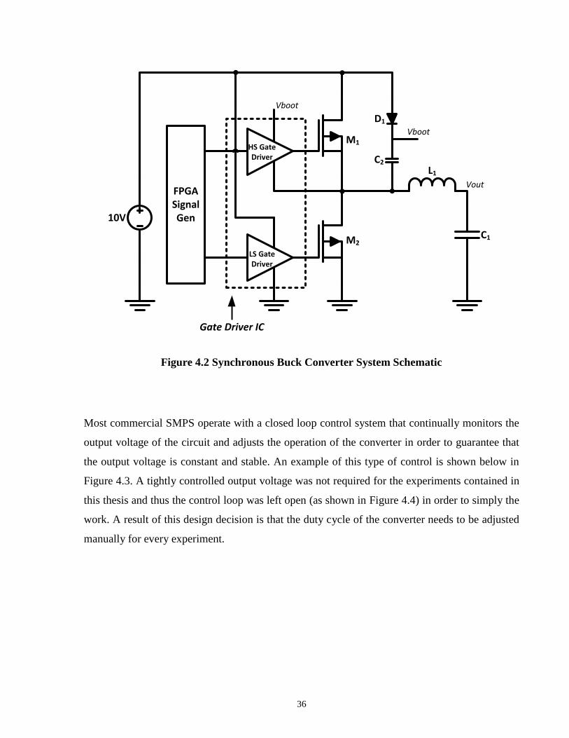
buck converter of the topology shown in Figure 4.2. The system utilizes two International
Rectifier IRF8707GTRPBF power MOSFETs (data sheet can be found in Appendix A) for M1
and M2 with 9.3 nC gate charge at 5 V and on-resistance of 9.3 mΩ when VGS = 10V. Gate drive
voltages of 10 V were used to drive M1 and M2. A Susumu PCMC135T-1R0MF inductor with an
inductance of 1 µH was used as the output inductance L1. A surface mount ceramic capacitor
with a capacitance of 20 μF was used as the output capacitance C1. The bootstrapping circuit
(composed of a diode and capacitor, D1 and C2) was used to provide the voltage required to turn
on the high-side power MOSFET M1. A Diodes Inc. SD103BWS-7-F Schottky diode was
utilized for D1, it has a rated maximum average current of 350 mA and a forward voltage drop of
600 mV when conducting 200mA of current. A 22 μF ceramic capacitor was used for C2.
36
M1
L1
C1
10V
FPGASignal Gen
M2
D1
C2
Vboot
Vboot
Vout
HS Gate Driver
LS Gate Driver
Gate Driver IC
Figure 4.2 Synchronous Buck Converter System Schematic
Most commercial SMPS operate with a closed loop control system that continually monitors the
output voltage of the circuit and adjusts the operation of the converter in order to guarantee that
the output voltage is constant and stable. An example of this type of control is shown below in
Figure 4.3. A tightly controlled output voltage was not required for the experiments contained in
this thesis and thus the control loop was left open (as shown in Figure 4.4) in order to simply the
work. A result of this design decision is that the duty cycle of the converter needs to be adjusted
manually for every experiment.

37
ControllerSwitch Network +
Output Filters
Voltage Sensor
VIN
Control Signals VOUT
Figure 4.3 Typical Voltage Controlled SMPS Topology
Digital ControllerSwitch Network +
Output Filters
VIN
Control Signals VOUT
Manual Settings
Figure 4.4 Open Loop SMPS Topology
The system described above was implemented on a two-layer FR4 PCB. The design of the top
and bottom copper layers are as shown in Figure 4.5. The assembled PCB is as shown in Figure
4.6. Power was supplied to and removed from the converter using Emerson Network Power
Connectivity Solutions 108-0740-001 banana plug receptacles. The digital signals driving the
gate driver IC were supplied with an Altera Cyclone II FPGA DE2 Development Board. The
DE2 board allowed for manual control of the duty cycle, dead time, Tpost and Tpre values. The
Altera DE2 board was connected to the converter via a 40pin header connection.
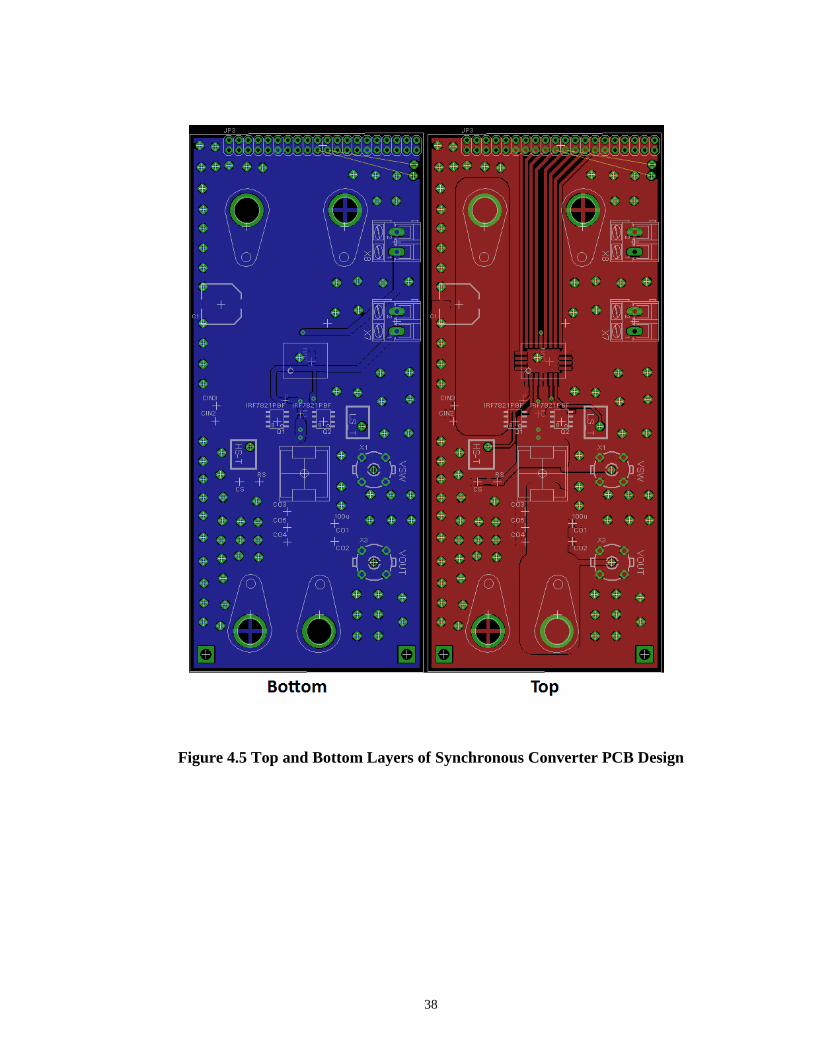
38
Figure 4.5 Top and Bottom Layers of Synchronous Converter PCB Design
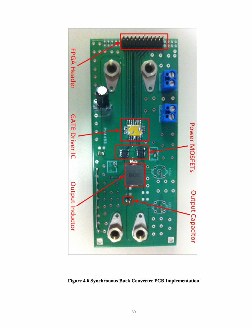
39
Figure 4.6 Synchronous Buck Converter PCB Implementation
40
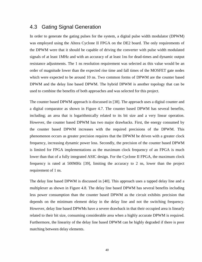
4.3 Gating Signal Generation
In order to generate the gating pulses for the system, a digital pulse width modulator (DPWM)
was employed using the Altera Cyclone II FPGA on the DE2 board. The only requirements of
the DPWM were that it should be capable of driving the converter with pulse width modulated
signals of at least 1MHz and with an accuracy of at least 1ns for dead-times and dynamic output
resistance adjustments. The 1 ns resolution requirement was selected as this value would be an
order of magnitude lower than the expected rise time and fall times of the MOSFET gate nodes
which were expected to be around 10 ns. Two common forms of DPWM are the counter based
DPWM and the delay line based DPWM. The hybrid DPWM is another topology that can be
used to combine the benefits of both approaches and was selected for this project.
The counter based DPWM approach is discussed in [38]. The approach uses a digital counter and
a digital comparator as shown in Figure 4.7. The counter based DPWM has several benefits,
including; an area that is logarithmically related to its bit size and a very linear operation.
However, the counter based DPWM has two major drawbacks. First, the energy consumed by
the counter based DPWM increases with the required precisions of the DPWM. This
phenomenon occurs as greater precision requires that the DPWM be driven with a greater clock
frequency, increasing dynamic power loss. Secondly, the precision of the counter based DPWM
is limited for FPGA implementations as the maximum clock frequency of an FPGA is much
lower than that of a fully integrated ASIC design. For the Cyclone II FPGA, the maximum clock
frequency is rated at 500MHz [39], limiting the accuracy to 2 ns, lower than the project
requirement of 1 ns.
The delay line based DPWM is discussed in [40]. This approach uses a tapped delay line and a
multiplexer as shown in Figure 4.8. The delay line based DPWM has several benefits including
less power consumption than the counter based DPWM as the circuit exhibits precision that
depends on the minimum element delay in the delay line and not the switching frequency.
However, delay line based DPWMs have a severe drawback in that their occupied area is linearly
related to their bit size, consuming considerable area when a highly accurate DPWM is required.
Furthermore, the linearity of the delay line based DPWM can be highly degraded if there is poor
matching between delay elements.

41
Digital Counter
Duty Cycle[N]
Count[N]
PWM Out
Input Clock
+_
Figure 4.7 Counter Based DPWM Topology
Delay[1] Delay[2] Delay[2N]
2N to 1 MUX
Duty Cycle[N]
PWM OutInput Clock
Edge TriggeredSR-Latch
R
S
Figure 4.8 Delay Line Based DPWM Topology
An often employed solution to the tradeoffs between the counter based and delay line based
DPWMs is the hybrid DPWM [41]. The hybrid DPWM essentially works by combining the
counter based and delay line based DPWM approaches. In order to meet the accuracy
requirements of this project a hybrid DPWM similar to the one shown in Figure 4.9 was
employed. With this topology, the (N-1) most significant bits of the pulse width modulation are
determined by the digital counter and the least significant bit is supplied by the delay line. This
arrangement allows the DPWM to achieve an accuracy of 1 ns without requiring the counter to
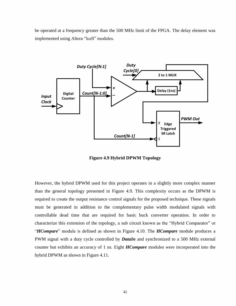
42
be operated at a frequency greater than the 500 MHz limit of the FPGA. The delay element was
implemented using Altera “lcell” modules.
Digital Counter
Duty Cycle[N:1]
Count[N-1:0]
PWM Out
Input Clock
+_
Delay (1ns)
2 to 1 MUX
Duty Cycle[0]
Edge Triggered SR Latch
Count[N-1]
R
S
Figure 4.9 Hybrid DPWM Topology
However, the hybrid DPWM used for this project operates in a slightly more complex manner
than the general topology presented in Figure 4.9. This complexity occurs as the DPWM is
required to create the output resistance control signals for the proposed technique. These signals
must be generated in addition to the complementary pulse width modulated signals with
controllable dead time that are required for basic buck converter operation. In order to
characterize this extension of the topology, a sub circuit known as the “Hybrid Comparator” or
“HCompare” module is defined as shown in Figure 4.10. The HCompare module produces a
PWM signal with a duty cycle controlled by DataIn and synchronized to a 500 MHz external
counter but exhibits an accuracy of 1 ns. Eight HCompare modules were incorporated into the
hybrid DPWM as shown in Figure 4.11.

43
DataIn[N:0]
Count[N-1:0]
Out
+_
Delay (1ns)
2 to 1 MUX
DataIn[0]DataIn[N:1]
Edge Triggered SR LatchCount[N-1]
Figure 4.10 Topology of the HCompare Module
The augmented Hybrid DPWM circuit shown in Figure 4.11 was implemented on the DE2 using
Verilog HDL code. The DC variable refers to the Duty Cycle command provided to the DPWM,
the DTn variable refers to the negative edge dead time command provided to the DPWM, the
DTp variable refers to the positive edge dead time command provided to the DPWM and Tpre and
Tpost are the output resistance control variables defined in Section 0. The “Digital Logic” block is
composed of static logic elements that combine the signals from the HCompare modules and
produces the gating signals and the output resistance control signals.
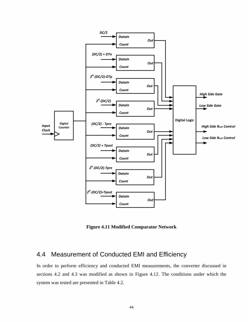
44
DC/2
(DC/2) + DTn
2N-(DC/2)-DTp
2N-(DC/2)
(DC/2) - Tpre
(DC/2) + Tpost
2N-(DC/2)-Tpre
2N-(DC/2)+Tpost
Digital CounterInput
Clock
Count
DataIn
Count
DataIn
Count
DataIn
Count
DataIn
Count
DataIn
Count
DataIn
Count
DataIn
Count
DataIn
Out
Out
Out
Out
Out
Out
Out
Out
Digital Logic
High Side Gate
Low Side Gate
High Side Rout Control
Low Side Rout Control
Figure 4.11 Modified Comparator Network
4.4 Measurement of Conducted EMI and Efficiency
In order to perform efficiency and conducted EMI measurements, the converter discussed in
sections 4.2 and 4.3 was modified as shown in Figure 4.12. The conditions under which the
system was tested are presented in Table 4.2.

45
Figure 4.12 Circuit Diagram of Experimental Test Setup
Table 4.2 Operating Conditions for Testing
Parameter Value
Vin 10 V
Vout 1.2 V
C 20 µF
L 1 µH
Iout 2 A
fsw 1 MHz

46
4.4.1 Measurement of Conducted EMI
Conducted EMI was measured using a similar technique to [34]. With this technique, a Tektronix
TCPA300 current probe measures the common mode current flowing between the 10V supply
and the converter. The signal from the current probe is then amplified using a Tektronix TCP312
current probe amplifier and the signal is supplied to an HP8591E spectrum analyzer. With this
setup, the spectrum of the current drawn from the primary power supply can be measured
between 150 kHz and 30 MHz, the FCC frequency range of interest for conducted EMI. The
system can perform conducted EMI measurements at frequencies up to 100 MHz. The 100 MHz
limitation arises as this is the TCPA300 current probes maximum bandwidth. With this topology,
the spectrum analyzer presents spectrum data with dBµA units. In order to convert these units to
dBµV, (4.1) must be used [42]. However (4.1) simplifies to (4.2) as the transfer impedance (Zt)
is equivalent to 1 for the Tektronix current probe system that was used.
( ) (4.1)
(4.2)
4.4.2 Measurement of Efficiency
Efficiency of the system (η) was determined by measuring the exact output and input voltages
(Vout and Vin respectively) using voltmeters, measuring the input and output currents using
ammeters (Iout and Iin respectively) and applying equation (4.3). The power consumption of the
FPGA was ignored as the digital circuits that it contains could be easily migrated to an ASIC
implementation where their power consumption would be drastically reduced.
(4.3)

47
4.5 Measurement of Radiated EMI
In order to perform radiated EMI measurements, the converter discussed in sections 4.2 and 4.3
was placed in an RF shielded anechoic chamber. Radiated emissions were then detected using a
simple dipole antenna and were analyzed using a HP8591E spectrum analyzer with a resolution
bandwidth of 1 kHz. Figure 4.14 and Figure 4.15 show the test setup that was used to perform
the radiated EMI tests. The resonant frequency of the dipole antenna was set to be 88 MHz. The
resonant frequency was selected as 88 MHz is the boundary frequency between the two lowest
FCC radiated emissions ranges (30 MHz to 88 MHz and 88MHz to 216 MHz). Thus, this
resonant frequency allowed for measurements within both of these EMI frequency ranges.
Furthermore, both of these frequency ranges are close to the measured gate ringing frequency of
approximately 70 MHz. Given (4.4), the dipole antenna was constructed with a structure shown
in Figure 4.13 and a length (L) of 1.625 m [43]. For simplicity, the gain of the antenna and
cabling connecting it to the spectrum analyzer was neglected. Thus, to convert the dBµV reading
of the spectrum analyzer to the µV/m units required by the FCC radiated emission standards,
(4.5) was employed [42]. Furthermore, the height of the antenna (H) was selected to be 1.4 m in
accordance with the guidelines set forth by [44].
(4.4)
(( ) ) (4.5)
L
H
Signal Out
BNC Coaxial Cable
Signal Ground
Figure 4.13 Radiated EMI Dipole Antenna Structure

48
5m
Anechoic Chamber
1.4m
DUT
Antenna
Figure 4.14 Radiated EMI Test Setup (Side View)
5m
Anechoic Chamber
DUT
Antenna
Figure 4.15 Radiated EMI Test Setup (Top View)

49
4.6 Determining the Effects of Tpre and Tpost
The conducted EMI (as discussed in 4.4.1) and the efficiency of the converter (as discussed in
4.4.2) were measured while the timing parameters Tpre and Tpost were adjusted. This operation
was performed in order to observe the effects that these parameters exert over the system. With
this testing, the optimal values for Tpre and Tpost were extracted. For the tests in this section, the
conducted EMI was measured between 30 MHz and 100 MHz, which is above the FCC
conducted EMI range of 150 kHz to 30 MHz. This approach was taken as it was observed that
the greatest reduction in conducted EMI occurred at the same frequency as the gate node ringing
which was observed to be approximately 70 MHz and the goal of this phase of testing was to
find the values of Tpre and Tpost that reduce ringing the most.
4.6.1 The Effects of the Tpre Variable
Figure 4.16 shows the improvement in peak conducted EMI as a function of the Tpre variable. In
this graph, improvement is measured as the difference in peak conducted EMI between the
proposed technique and the low output resistance mode.
Figure 4.16 Improvement in Conducted EMI VS Tpre
0
0.5
1
1.5
2
2.5
3
0 5 10 15 20
Co
nd
uct
ed
EM
I Im
pro
vem
en
t [d
Bµ
V]
Tpre [ns]

50
The low output resistance mode being defined as the mode when all gate drive segments are
constantly enabled, lowering the gate drive resistance as much as possible. For this measurement,
Tpost was set at 10 ns and all dead-time values were selected to be 8 ns. From this graph it can be
seen that beyond a minimum value of approximately 3 ns, the value of Tpre has little bearing on
the conducted EMI of the converter.
Figure 4.17 shows the converter efficiency as a function of the Tpre variable. As can be seen in
this graph, the effect that Tpre has on the efficiency of the converter is negligible. When Tpre is
varied from 0 ns to over 20 ns, the efficiency of the converter varies by less than 0.5% for values
of Tpre above 3ns. Thus, Tpre has little effect on the overall efficiency of the converter above a
magnitude of 3 ns.
Figure 4.17 Converter Efficiency VS Tpre
From the analysis of Figure 4.16 and Figure 4.17, it can be concluded that the value of Tpre only
needs to satisfy two requirements. First, the value of Tpre must be sufficiently large that that it
does not inhibit conducted EMI reduction. Second, the value of Tpre must be sufficiently small
75.000%
75.500%
76.000%
76.500%
77.000%
77.500%
78.000%
0 5 10 15 20
Effi
cie
ncy
[%
]
Tpre [ns]

51
such that it does not interfere with the normal operation of the converter. Given these
requirements and the data from Figure 4.16 and Figure 4.17, Tpre was selected to have the value
of 5 ns. This selection is larger than the minimum Tpre determined by analyzing Figure 4.16 but
not so large that it inhibits operation of the converter.
4.6.2 The Effects of the Tpost Variable
Figure 4.18 shows the improvement in peak conducted EMI as a function of the Tpost variable. In
this graph, improvement is measured as the difference in peak conducted EMI between the
proposed technique and the low output resistance mode. The low output resistance mode being
defined as the mode when all gate drive segments are constantly enabled, lowering the gate drive
resistance as much as possible. For these measurements, Tpre was set as 5 ns and all dead time
values were selected as 8 ns. As shown in Figure 4.18, the improvement in conducted EMI is
reduced for very high (over 10 ns) values of Tpost. This result makes sense as large values of Tpost
will mean that the output resistance is held low long after the gate transition has passed and
ringing at the gate node is not dampened.
Figure 4.18 Improvement in Conducted EMI VS Tpost
0
2
4
6
8
10
12
6 11 16 21 26 31
Co
nd
uct
ed
EM
I Im
pro
vem
en
t [d
Bµ
V]
Tpost [ns]

52
Figure 4.19 shows the efficiency of the converter as a function of Tpost. From this graph it can be
seen that the efficiency of the converter decreases slightly for low values of Tpost but that Tpost has
a diminished influence on efficiency when its value exceeds approximately 10 ns. This
observation makes sense as low values of Tpost should cause the converter to function identical to
the case where the output resistance is held constantly high and the switching loss is increased,
causing power loss. Furthermore, large values of Tpost cause the converter to function identical to
the case where the output resistance is held constantly low.
Figure 4.19 Converter Efficiency VS Tpost
Given the data of Figure 4.18 and Figure 4.19, a value of 8 ns was selected for Tpost. This
particular value was selected as this value causes a significant reduction in ringing while not
reducing the efficiency of the converter. Furthermore, the value of 8 ns matches the rise time and
fall time of the gate nodes when the output resistance of the gate drivers is set to the lowest
possible value (only one segment enabled), which was measured to be approximately 8 ns. Thus,
the Tpost value has been selected to be just long enough that the entire gate node transition occurs
during the low output resistance period.
69.000%
70.000%
71.000%
72.000%
73.000%
74.000%
75.000%
76.000%
77.000%
78.000%
6 11 16 21 26 31
Co
nve
rte
r Ef
fici
en
cy [
%]
Tpost [ns]

53
4.7 Voltage Waveforms
In order to determine the effect that the proposed technique has on ringing within the system,
voltage waveforms for the high side gate, low side gate and the switching node of the converter
were measured. These measurements were performed using a Tektronix MSO 4034 oscilloscope.
These particular voltage waveforms were monitored as it is intended for the proposed technique
to directly control the ringing of these nodes in order to produce a reduction in EMI without
degrading efficiency. Thus, for the theory of the presented technique to be validated, it must be
confirmed that the effects on EMI and efficiency result from changes in the behavior of these
voltage waveforms.
4.7.1 Voltage Waveform Measurement Strategy
In order to observe the proposed technique, measurements were organized into three tests, each
test having a particular gate drive output resistance. During this testing, Tpost, Tpre and the
maximum/minimum resistance values were identical for both the rising and falling edge of the
gate driver. Furthermore, these variables were identical for both high side and low side gate
drivers.
During the first test, the output resistance of the gate drivers was set to be constantly high. This
operation was achieved by only activating one of the seven segments of both gate drivers. By
performing this experiment, a situation where switching loss is significant but conducted EMI is
reduced can be examined.
During the second test, the output resistance of the gate drivers was set to be constantly low. This
operation was achieved by activating all of the seven segments of both gate drivers. By
performing this experiment, a situation where switching loss is reduced but conducted EMI is
significant can be examined.
During the third test, the output resistance of the drivers was operated using the proposed
technique. The low output resistance setting was achieved by activating all seven segments of the
gate drivers. The high output resistance setting was achieved by activating one of the seven
segments of the gate drivers. Values for Tpost and Tpre were set using the information shown in

54
Section 4.6. The previous two experiments provided a baseline set of measurements, against
which results from this experiment could be compared. In particular, it needed to be determined
if the proposed technique achieved the conducted EMI spectrum of the high output resistance
mode while maintaining the efficiency of the low output resistance mode.
4.7.2 Voltage Waveform Measurements
In order to measure the effects of the presented technique, the voltage waveforms were measured
under the three operating conditions outlined in 4.7.1. The voltage waveform measurements for
the high side gate node, low side gate node and the switching node of the converter for high gate
drive output resistance and low gate drive output resistance are shown in Figure 4.20 and Figure
4.21 respectively.
When the converter is operated with a high gate driver output resistance it can be seen that the
rise times and fall times of the low side and high side gate nodes are approximately 40 ns.
Overshoot of 8 V for the high side gate node and 0 V for the low side gate node is observed.
Furthermore, undershoot of 8 V for the high side gate node and 4 V for the low side gate node is
observed.
When the converter is operated with a low gate driver output resistance it can be seen that the
rise times and fall times of the low side and high side gate nodes are approximately 8 ns.
Overshoot of 16 V for the high side gate node and 8 V for the low side gate node is observed.
Furthermore, undershoot of 16 V for the high side gate node and 6 V for the low side gate node
is observed.
During the low output resistance mode, a decrease in rise time of 32 ns is observed relative to the
high output resistance mode. However, a significant increase in the overshoot and undershoot of
the gate nodes is also observed for the low output resistance mode, increasing the ringing at these
nodes. Furthermore, the increase in gate node ringing exhibited by the low output resistance
mode is causing an increase in ringing at the switching node as well. This observation confirms
the theory outlined in Section 0 that there is a tradeoff between gate node ringing and the
transition times of the power switches.

55
Figure 4.20 Voltage Measurements For High Output Resistance (One Segment Enabled)
Figure 4.21 Voltage Measurements For Low Output Resistance (All Segments Enabled)

56
Figure 4.22 shows the voltage waveforms of the converter during operation of the proposed
technique. Tpost was selected as 8 ns and Tpre was selected as 5 ns. For this graph, the rise times
and fall times of the gate nodes were measured to be approximately 8 ns. Overshoot of 4 V for
the high side gate node and 6 V for the low side gate node is observed. Furthermore, undershoot
16 V for the high side gate node and 0.5V for the low side gate node is observed.
These observations indicate that the proposed technique is reducing gate node ringing during the
rising edge of the high side gate and the falling edge of the low side gat node. However, the
technique is not effectively dampening the ringing that occurs at the falling edge of the high side
gate node. Thus, despite the inability to eliminate all the ringing at the gate node, the proposed
technique is reducing some ringing without introducing longer transition times.
Figure 4.22 Voltage Measurements For Proposed Technique

57
4.8 Conducted EMI Spectrum and Efficiency Measurements
In order to measure the effects of the presented technique, the conducted EMI spectrum of the
converter is measured under the three operating conditions outlined in 4.7.1. The conducted EMI
spectrums of the converter for high gate drive output resistance and low gate drive output
resistance are shown in Figure 4.23 and Figure 4.24 respectively.
When the converter is operated with a high gate driver output resistance it can be seen that the
conducted EMI spectrum between 20 MHz and 30 MHz has a peak magnitude of 28 dBµV.
When the converter is operated with a low gate driver output resistance it can be seen that the
conducted EMI spectrum between 20 MHz and 30 MHz has a peak magnitude of 30 dBµV.
These measurements clearly show that the reduction in ringing that occurs when the gate drive
resistance is increased causes a reduction in the conducted EMI emitted by the converter. This
observation validates the theory presented in section 3.2 that the ringing at the gate node
contributes to the conducted EMI of the converter.
Table 4.3 shows the efficiency of the converter for the three operating conditions. Looking at the
efficiency for the high output resistance and low output resistance modes, it can be seen that an
increased output resistance does diminish the efficiency of the converter by 2.3%. This
observation validates the theory outlined in section 3.1 concerning the effects of increased
MOSFET transition times and switching loss.

58
Figure 4.23 Conducted EMI Spectrum for High Output Resistance (One Segment Enabled)
Figure 4.24 Conducted EMI Spectrum for Low Output Resistance (All Segments Enabled)

59
Figure 4.25 shows the conducted EMI spectrum of the converter during operation of the
proposed technique. Tpost was selected as 8 ns and Tpre was selected as 5 ns. From this graph it
can be seen that the conducted EMI spectrum between 20 MHz and 30 MHz has a peak
magnitude of 23 dBµV. Thus, there is an improvement of 7 dBµV between 20 MHz and 30 MHz
relative to the low output resistance mode. Furthermore, there is an improvement of 5 dBµV
relative to the high output resistance mode. This result indicates that the proposed technique
inhibits gate node ringing even more effectively than an increased gate driver output resistance.
The efficiency of the converter when operating using the proposed technique was 76.5 %. Thus,
the proposed technique provided an improvement in conducted EMI without a significant
reduction in converter efficiency.
Figure 4.25 Conducted EMI Spectrum for Proposed Technique
Table 4.3 Converter Efficiency for Different Modes of Operation
Operation Mode Converter Efficiency
High Output Resistance 74.3 %
Low Output Resistance 76.6 %
Adjustable Driving Strength 76.5 %

60
4.9 Radiated EMI Measurements
In order to fully measure the effects of the presented technique, the radiated EMI spectrum of the
converter is measured under the three operating conditions outlined in 4.7.1. Specifically, the
spectrum from 88 MHz to 216 MHz was measured as this is the only FCC defined radiated EMI
frequency range that the proposed technique was found to have influenced. The radiated EMI
spectrums of the converter for low gate drive output resistance and high gate drive output
resistance are shown in Figure 4.27 and Figure 4.28 respectively.
Additionally, the radiated EMI spectrum of the anechoic chamber was measured while the
converter was not in operation, the results of which are shown in Figure 4.26. A small amount of
RF interference is leaking in the chamber between the frequencies of 88 MHz and 110 MHz.
This observation makes sense as broadcast FM radio uses the frequencies of 87.5 MHz to 108
MHz and the anechoic chamber in use was situated only 2 km from the CN Tower, which
supports several very strong FM transmitters.
When the converter is operated with a low gate drive output resistance it can be seen that the
radiated EMI spectrum between 88 MHz and 216 MHz has a peak magnitude of 700 µV/m.
When the converter is operated with a high gate driver output resistance it can be seen that the
conducted EMI spectrum between 88 MHz and 216 MHz has a peak magnitude of 285 µV/m.
It is also observed that while the peak radiated EMI occurs near 90 MHz a secondary occurrence
of radiated EMI was observed near 135 MHz. When the converter is operated with low gate
driver output resistance it can be seen that the radiated EMI spectrum near 135 MHz has a peak
magnitude of 94 µV/m. When the converter is operated with a high gate driver output resistance
it can be seen that the conducted EMI spectrum near 135 MHz has a peak magnitude of 45
µV/m.
These measurements clearly show that the reduction in ringing that occurs when the gate drive
resistance is increased causes a reduction in the radiated EMI emitted by the converter. This
observation validates the theory presented in section 3.2 that the ringing at the gate node
contributes to the radiated EMI of the converter.

61
Figure 4.26 Ambient Radiated EMI Spectrum
Figure 4.27 Radiated EMI Spectrum for Low Output Resistance (All Segments Enabled)
0.00E+00
1.00E+02
2.00E+02
3.00E+02
4.00E+02
5.00E+02
6.00E+02
7.00E+02
8.00E+02
8.80E+07 1.08E+08 1.28E+08 1.48E+08 1.68E+08 1.88E+08 2.08E+08
Rad
iate
d E
MI M
easu
rem
ent
[uV
/m]
Frequency[Hz]
0.00E+00
1.00E+02
2.00E+02
3.00E+02
4.00E+02
5.00E+02
6.00E+02
7.00E+02
8.00E+02
8.80E+07 1.08E+08 1.28E+08 1.48E+08 1.68E+08 1.88E+08 2.08E+08
Rad
iate
d E
MI M
easu
rem
ent
[uV
/m]
Frequency[Hz]

62
Figure 4.28 Radiated EMI Spectrum for High Output Resistance (One Segment Enabled)
Figure 4.29 Radiated EMI Spectrum for Proposed Technique
0.00E+00
1.00E+02
2.00E+02
3.00E+02
4.00E+02
5.00E+02
6.00E+02
7.00E+02
8.00E+02
8.80E+07 1.08E+08 1.28E+08 1.48E+08 1.68E+08 1.88E+08 2.08E+08
Rad
iate
d E
MI M
easu
rem
ent
[uV
/m]
Frequency[Hz]
0.00E+00
1.00E+02
2.00E+02
3.00E+02
4.00E+02
5.00E+02
6.00E+02
7.00E+02
8.00E+02
8.80E+07 1.08E+08 1.28E+08 1.48E+08 1.68E+08 1.88E+08 2.08E+08
Rad
iate
d E
MI M
easu
rem
ent
[uV
/m]
Frequency[Hz]
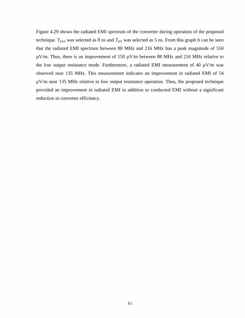
63
Figure 4.29 shows the radiated EMI spectrum of the converter during operation of the proposed
technique. Tpost was selected as 8 ns and Tpre was selected as 5 ns. From this graph it can be seen
that the radiated EMI spectrum between 88 MHz and 216 MHz has a peak magnitude of 550
µV/m. Thus, there is an improvement of 150 µV/m between 88 MHz and 216 MHz relative to
the low output resistance mode. Furthermore, a radiated EMI measurement of 40 µV/m was
observed near 135 MHz. This measurement indicates an improvement in radiated EMI of 54
µV/m near 135 MHz relative to low output resistance operation. Thus, the proposed technique
provided an improvement in radiated EMI in addition to conducted EMI without a significant
reduction in converter efficiency.
64
Chapter 5 Conclusions and Future Work
A segmented gate driver technique is presented in this work with goal of reducing
electromagnetic interference. The overall design of the gate driver and the experimental results
of the work are presented in this section.
5.1 Thesis Summary
Switch mode power supplies built using discrete components are an essential subsystem of
modern commercial electronics. As discrete SMPS are being operated at higher frequencies, the
need to reduce EMI is becoming critical. Reducing EMI is important to system designers as
excess EMI can cause devices connected to the SMPS or even simply located nearby to
malfunction. Periodic current draw and ringing at nodes within the SMPS contribute heavily to
EMI.
In this thesis, a segmented gate driving technique is developed and shown to reduce conducted
and radiated EMI in a discrete synchronous buck converter without a significant reduction in
efficiency. This operation is achieved by leveraging the fact that segmentation of the gate driver
means that the output resistance of the gate driver can be dynamically adjusted on the fly. With
this ability, the output resistance of the gate driver can be set low during a transition to reduce
switching loss and then set high after the transition has passed in order to dampen any ringing
that may occur at the gate node. Thus, the tradeoff between switching loss and EMI resulting
from gate node ringing can be eliminated.
The technique was verified by incorporating a segmented gate driver IC into a discrete buck
converter system. An improvement in CEMI of 7dBµV between 20 MHz and 30 MHz and an
improvement in REMI of 150 uV/m between 88 MHz and 216 MHz was realized at an output
load of 2 A.

65
5.2 Future Work
The suppression of EMI in an affordable and elegant manner is a highly desired commercial
goal. As such, work on this topic will continue into the foreseeable future. Future work on this
project can be summarized into four distinct approaches.
1. The impact on EMI of using more than two settings for Rout should be examined. The
current approach has only investigated the effects of switching the gate driver between a
single low and single high Rout value, thus utilizing only two settings for the output
resistance. Future work should investigate whether or not using intermediate values for Rout
has any positive impact on EMI or efficiency. This operation will likely require a
redefinition of the gate driver switching waveform beyond the simple variables of Tpre and
Tpost.
2. The impact of using a larger number of segments should be investigated. The current IC
used for testing has only seven segments. Thus, the ratio between the largest and the
smallest Rout values is limited to a factor of seven. Future work should involve fabricating a
new gate driver IC with a larger number of gate driver segments, perhaps 100 or even 1000
segments. This level of segmentation will likely not increase the die size of the gate driver
by much but will allow a greater ratio between the smallest and largest output resistances
that the gate driver can be set to.
3. The suitability of the presented technique for insulated gate bipolar transistors (IGBTs)
should be examined. IGBTs are becoming increasingly common in high voltage systems
(500 V and above). Future work should investigate whether or not the technique presented
has the ability to reduce EMI when used with IGBT devices instead of power MOSFETs.
This work will require a new segmented gate driver IC capable of driving the larger gate
capacitances inherent to modern commercial IGBT devices.

66
References
[1] Feng Lin; Chen, D.Y.; , "Reduction of power supply EMI emission by switching
frequency modulation," Power Electronics, IEEE Transactions on , vol.9, no.1,
pp.132-137, Jan 1994
[2] Barnes, Ben; MacDonald, Murray; Piwowar, Joseph; , "EMI Requirements for
Power Supplies and Description of an Enclosed Open Field Test
Site," Telecommunications Energy Conference, 1986. INTELEC '86. International,
vol., no., pp.675-679, 19-22 Oct. 1986
[3] Sali, S.; , "Radiated interference," The 'Hows' and 'Whys' of EMC Design (Ref. No.
1999/001), IEE Seminar on , vol., no., pp.2/1-2/7, 1999
[4] Stratakos, A.J.; Sanders, S.R.; Brodersen, R.W.; , "A low-voltage CMOS DC-DC
converter for a portable battery-operated system," Power Electronics Specialists
Conference, PESC '94 Record., 25th Annual IEEE , vol., no., pp.619-626 vol.1, 20-
25 Jun 1994
[5] Dancy, A.P.; Amirtharajah, R.; Chandrakasan, A.P.; , "High-efficiency multiple-
output DC-DC conversion for low-voltage systems," Very Large Scale Integration
(VLSI) Systems, IEEE Transactions on , vol.8, no.3, pp.252-263, June 2000
[6] Maksimovic, D.; Zane, R.; Erickson, R.; , "Impact of digital control in power
electronics," Power Semiconductor Devices and ICs, 2004. Proceedings. ISPSD
'04. The 16th International Symposium on , vol., no., pp. 13- 22, 24-27 May 2004
[7] Thomas, R.; Li, F.; Garrett, C.; , "Prediction of radiated EMI from high frequency
power converters," Power Electronics and Variable Speed Drives, 2000. Eighth
International Conference on (IEE Conf. Publ. No. 475) , vol., no., pp.80-85, 2000

67
[8] Vilathgamuwa, M.; Deng, J.; Tseng, K.J.; , "EMI suppression with switching
frequency modulated DC-DC converters ," Industry Applications Magazine, IEEE ,
vol.5, no.6, pp.27-33, Nov/Dec 1999
[9] Ran, L.; Gokani, S.; Clare, J.; Bradley, K.J.; Christopoulos, C.; , "Conducted
electromagnetic emissions in induction motor drive systems. I. Time domain
analysis and identification of dominant modes ," Power Electronics, IEEE
Transactions on , vol.13, no.4, pp.757-767, Jul 1998
[10] Skibinski, G.L.; Kerkman, R.J.; Schlegel, D.; , "EMI emissions of modern PWM AC
drives," Industry Applications Magazine, IEEE , vol.5, no.6, pp.47-80, Nov/Dec
1999
[11] Ogasawara, S.; Ayano, H.; Akagi, H.; , "Measurement and reduction of EMI
radiated by a PWM inverter-fed AC motor drive system," Industry Applications,
IEEE Transactions on , vol.33, no.4, pp.1019-1026, Jul/Aug 1997
[12] Antonini, G.; Cristina, S.; Orlandi, A.; , "EMC characterization of SMPS devices:
circuit and radiated emissions model," Electromagnetic Compatibility, IEEE
Transactions on , vol.38, no.3, pp.300-309, Aug 1996
[13] Arbetter, B.; Erickson, R.; Maksimovic, D.; , "DC-DC converter design for battery-
operated systems," Power Electronics Specialists Conference, 1995. PESC '95
Record., 26th Annual IEEE , vol.1, no., pp.103-109 vol.1, 18-22 Jun 1995
[14] Chia, Chu-Hsiang; Lei, Pui-Sun; Chang, Robert Chen-Hao; , "A high-efficiency
PWM DC-DC buck converter with a novel DCM control under light-load," Circuits
and Systems (ISCAS), 2011 IEEE International Symposium on , vol., no., pp.237-
240, 15-18 May 2011
[15] Robert W. Erickson, Dragan Maksimovic, “Principles of Steady-State Converter
Analysis,” in Fundamentals of Power Electronics, 2nd ed. New York: Springer,
2000, ch. 2, pp. 13–22.

68
[16] Robert W. Erickson, Dragan Maksimovic, “The Discontinuous Conduction Mode,”
in Fundamentals of Power Electronics, 2nd ed. New York: Springer, 2000, ch. 5,
pp. 108–112.
[17] Robert W. Erickson, Dragan Maksimovic, “Analysis of Converter Transfer
Functions,” in Fundamentals of Power Electronics, 2nd ed. New York: Springer,
2000, ch. 8, pp. 300.
[18] Yousefzadeh, V.; Maksimovic, D.; , "Sensorless optimization of dead times in DC-
DC converters with synchronous rectifiers," Power Electronics, IEEE Transactions
on , vol.21, no.4, pp. 994- 1002, July 2006
[19] S. Mapus, “Predictive gate drive boosts synchronous DC/DC power converter
efficiency,” APPL. Rep. SLUA281, Texas Instruments, Apr. 2003.
[20] Zhao, A.; Fomani, A.A.; Wai Tung Ng; , "One-step digital dead-time correction for
DC-DC converters," Applied Power Electronics Conference and Exposition
(APEC), 2010 Twenty-Fifth Annual IEEE , vol., no., pp.132-137, 21-25 Feb. 2010
[21] Robert W. Erickson, Dragan Maksimovic, “Switching Loss,” in Fundamentals of
Power Electronics, 2nd ed. New York: Springer, 2000, ch. 4, pp. 92–93.
[22] Fomani, A.A.; Ng, W.T.; , "A segmented gate driver with adjustable driving
capability for efficiency optimization," Power Electronics Conference (IPEC), 2010
International , vol., no., pp.1646-1650, 21-24 June 2010
[23] Fomani, A.A.; Wai Tung Ng; Shorten, A.; , "An integrated segmented gate driver
with adjustable driving capability," Energy Conversion Congress and Exposition
(ECCE), 2010 IEEE , vol., no., pp.2430-2433, 12-16
[24] Yuhui Chen; Lee, F.C.; Amoroso, L.; Ho-Pu Wu; , "A resonant MOSFET gate
driver with efficient energy recovery," Power Electronics, IEEE Transactions on ,
vol.19, no.2, pp. 470- 477, March 2004

69
[25] Robert W. Erickson, Dragan Maksimovic, “Steady Stae Equivalent Circuit
Modeling, Losses and Efficiency,” in Fundamentals of Power Electronics, 2nd ed.
New York: Springer, 2000, ch. 3, pp. 52.
[26] “PART 15--RADIO FREQUENCY DEVICES” Internet: http://www.access.gpo.gov/nara/cfr/waisidx_10/47cfr15_10.html, [August 18th, 2011].
[27] Robert W. Erickson, Dragan Maksimovic, “Input Filter Design,” in Fundamentals of
Power Electronics, 2nd ed. New York: Springer, 2000, ch. 10, pp. 37-3787.
[28] A. Shorten, A.A. Fomani, W.T. Ng, H. Nishio, and Y. Takahashi. “Reduction of
Conducted Electromagnetic Interference in SMPS using Programmable Gate
Driving Strength,” 23d International Symposium on Power Semiconductor Deviced
and ICs, San Diego, 2011.
[29] Byungcho Choi; Cho, B.H.; , "Intermediate line filter design to meet both
impedance compatibility and EMI specifications," Power Electronics, IEEE
Transactions on , vol.10, no.5, pp.583-588, Sep 1995
[30] Peng Li; Lehman, B.; , "Accurate loop gain prediction for DC-DC converter due to
the impact of source/input filter," Power Electronics, IEEE Transactions on , vol.20,
no.4, pp. 754- 761, July 2005
[31] McMurray, William; , "Optimum Snubbers for Power Semiconductors," Industry
Applications, IEEE Transactions on , vol.IA-8, no.5, pp.593-600, Sept. 1972
[32] U-Yaisom, C.; Khanngern, W.; Nitta, S.; , "The study and analysis of the conducted
EMI suppression on power MOSFET using passive snubber
circuits," Electromagnetic Compatibility, 2002 3rd International Symposium on ,
vol., no., pp. 561- 564, 21-24 May 2002
[33] McMurray, William; , "Selection of Snubbers and Clamps to Optimize the Design of
Transistor Switching Converters," Industry Applications, IEEE Transactions on ,
vol.IA-16, no.4, pp.513-523, July 1980

70
[34] Trescases, O.; Guowen Wei; Prodic, A.; Wai Tung; , "An EMI Reduction Technique
for Digitally Controlled SMPS," Power Electronics, IEEE Transactions on , vol.22,
no.4, pp.1560-1565, July 2007
[35] Trescases, O.; Guowen Wei; Wai Tung Ng; , "A Low-Power DC-DC Converter with
Digital Spread Spectrum for Reduced EMI," Power Electronics Specialists
Conference, 2006. PESC '06. 37th IEEE , vol., no., pp.1-7, 18-22 June 2006
[36] Strydom, J.T.; de Rooij, M.A.; van Wyk, J.D.; , "A comparison of fundamental gate-
driver topologies for high frequency applications," Applied Power Electronics
Conference and Exposition, 2004. APEC '04. Nineteenth Annual IEEE , vol.2, no.,
pp. 1045- 1052 vol.2, 2004
[37] Musunuri, S.; Chapman, P.L.; , "Improvement of light-load efficiency using width-
switching scheme for CMOS transistors," Power Electronics Letters, IEEE , vol.3,
no.3, pp. 105- 110, Sept. 2005
[38] Yousefzadeh, V.; Takayama, T.; Maksimovi, D.; , "Hybrid DPWM with Digital
Delay-Locked Loop," Computers in Power Electronics, 2006. COMPEL '06. IEEE
Workshops on , vol., no., pp.142-148, 16-19 July 2006
[39] “Section I. Cyclone II Device Family Data Sheet.” Internet:
http://www.altera.com/literature/hb/cyc2/cyc2_cii5v1_01.pdf, [August 18th 2011]
[40] Syed, A.; Ahmed, E.; Maksimovic, D.; Alarcon, E.; , "Digital pulse width modulator
architectures," Power Electronics Specialists Conference, 2004. PESC 04. 2004
IEEE 35th Annual , vol.6, no., pp. 4689- 4695 Vol.6, 20-25 June 2004
[41] Patella, B.J.; Prodic, A.; Zirger, A.; Maksimovic, D.; , "High-frequency digital PWM
controller IC for DC-DC converters," Power Electronics, IEEE Transactions on ,
vol.18, no.1, pp. 438- 446, Jan 2003
[42] “EMI EMC RF conversion formulas. ” Internet:
http://www.ahsystems.com/notes/TYPICAL_CONVERSION_FORMULAS.pdf,
[August 18th, 2011].

71
[43] “Low Frequency Antennas,” in The ARRL Antenna Book, 21st ed. USA: ARRL,
2007, ch. 6, pp. 6-16.
[44] “Making EMI Compliance Measurements.” Internet:
http://cp.literature.agilent.com/litweb/pdf/5990-7420EN.pdf, [August 18th, 2011].

72
Appendix A MOSFET Data Sheet

73

74

75
76

77

78

79

80