Embed Size (px)
Citation preview
EMI/EMC Characterization of Mixed Radio Frequency-Digital Circuits
Yakup Bayram, Zulfiqar Khan, Taesik Yang and John L. Volakis
Non-Linear RF Laboratory, ECE Dept.The Ohio State University
2015 Neil Ave., Columbus, OH, USA
Patrick Roblin, Saek Joo Doo and Sukkeun Myoung
ElectroScience Laboratory, ECE Dept.The Ohio State University
1320 Kinnear Road, Columbus, OH, 43212 USA
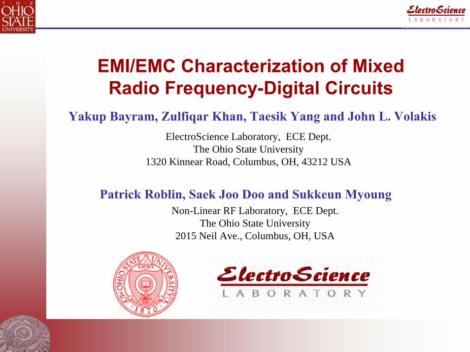
RF-Digital Circuits Subject to Intentional EMIUnderstand and predict the effects of electromagnetic interference
on electronic systems
Cable Bundles Subject to HPM Sources Mixed Signal Circuits Subject to HPM Sources
combined full wave numerical EM tools such as MLFMM MoM and
Modal MoM with cable bundle toolssuch as CableMod and CRIPTE
Analysis Method:Integration of numerical EM tools with
circuit tools such as ADS and HSPICE forRF/Analog/Digital Circuit Simulation
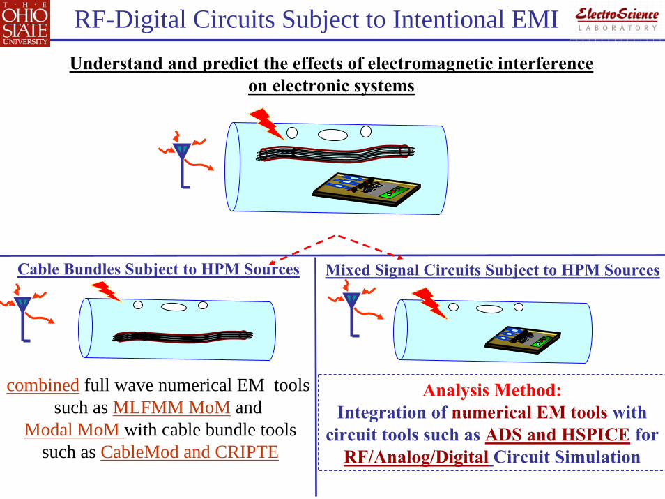
A specific problem
Inverter Subject to EMI
Inverter Subject to EMI with
Different Type Modulations
UnmodulatedEMI
Pulse modulated
EMI
Multi tone modulated
EMI
Observed Effects
Input
UndisturbedOutput
Disturbed OutputEMI Effects on• Timing Characteristics• Logic Behaviors
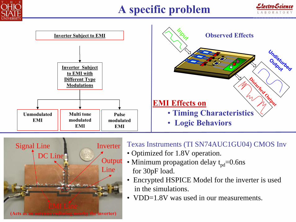
Texas Instruments (TI SN74AUC1GU04) CMOS Inv• Optimized for 1.8V operation.• Minimum propagation delay tpd=0.6ns
for 30pF load. • Encrypted HSPICE Model for the inverter is used
in the simulations. • VDD=1.8V was used in our measurements.
InverterSignal Line
EMI Line(Acts as an antenna radiating nearby the inverter)
DC Line OutputLine
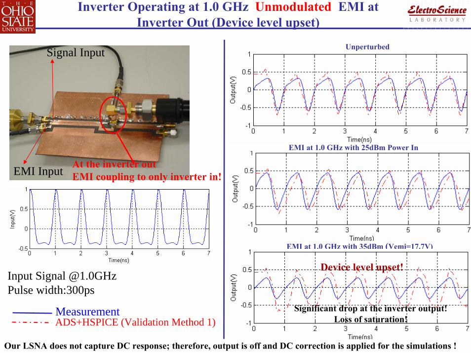
Inverter Operating at 1.0 GHz Unmodulated EMI at Inverter Out (Device level upset)
Signal Input
EMI Input
Input Signal @1.0GHzPulse width:300ps
Our LSNA does not capture DC response; therefore, output is off and DC correction is applied for the simulations !
Unperturbed
EMI at 1.0 GHz with 25dBm Power In
EMI at 1.0 GHz with 35dBm (Vemi=17.7V)
MeasurementADS+HSPICE (Validation Method 1)
Significant drop at the inverter output!Loss of saturation!
At the inverter outEMI coupling to only inverter in!
Device level upset!
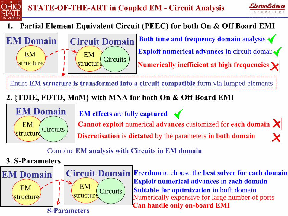
STATE-OF-THE-ART in Coupled EM - Circuit Analysis
EM DomainEM
structure
Circuit DomainEM
structureCircuits
1. Partial Element Equivalent Circuit (PEEC) for both On & Off Board EMI
Entire EM structure is transformed into a circuit compatible form via lumped elements
Both time and frequency domain analysis
Exploit numerical advances in circuit domain
Numerically inefficient at high frequencies
2. TDIE, FDTD, MoM with MNA for both On & Off Board EMI
EM DomainEM
structureCircuits
Combine EM analysis with Circuits in EM domain
EM effects are fully capturedCannot exploit numerical advances customized for each domainDiscretisation is dictated by the parameters in both domain
3. S-Parameters
EM DomainEM
structure
Circuit DomainEM
structureCircuits
S-Parameters
Freedom to choose the best solver for each domainExploit numerical advances in each domainSuitable for optimization in both domainNumerically expensive for large number of portsCan handle only on-board EMI
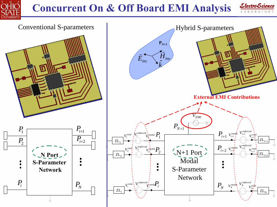
Concurrent On & Off Board EMI Analysis
N PortS-Parameter
Network
1P
2P
iP
1+iP2+iP
NP
kincEr
incHr
PN+1
N+1 PortModal
S-ParameterNetwork
1P
2P
iP
1+iP
2+iP
NP
1+NP
ZLi+1
modal1+iV total
1+iVenforced
iV 1+
ZLi+2
modal2+iV total
2+iVenforced
iV 2+
ZLN
modalNV total
NVenforcedNV
ZL1
modal1Vtotal
1VenforcedV1
ZL2
total2V
enforcedV2 modal2V
ZLi
totaliV
enforcediV modal
iV
EMIV
External EMI Contributions
Conventional S-parameters Hybrid S-parameters
PPPPP
P
PPPPPPPPPPPP
PP P PP
P PP P
PPP
P
P
PPP
P PPP
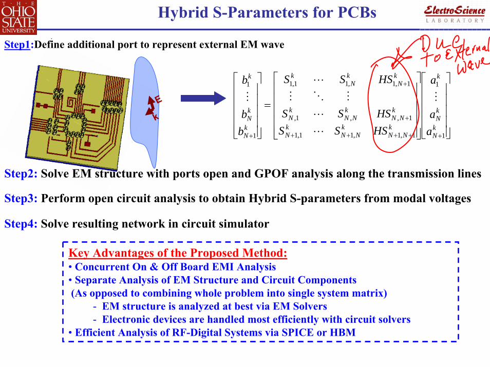
Step1:Define additional port to represent external EM wave
Step3: Perform open circuit analysis to obtain Hybrid S-parameters from modal voltages
Hybrid S-Parameters for PCBs
⎥⎥⎥⎥⎥
⎦
⎤
⎢⎢⎢⎢⎢
⎣
⎡
⎥⎥⎥⎥⎥
⎦
⎤
⎢⎢⎢⎢⎢
⎣
⎡
=
⎥⎥⎥⎥⎥
⎦
⎤
⎢⎢⎢⎢⎢
⎣
⎡
+++++
+
+
+kN
kN
k
kNN
kNN
kN
kNN
kNN
kN
kN
kN
k
kN
kN
k
aa
a
HSSSHSSS
HSSS
bb
b
1
1
1,1,11,1
1,,1,
1,1,11,1
1
1
M
L
L
MOM
L
M
Step2: Solve EM structure with ports open and GPOF analysis along the transmission lines
Step4: Solve resulting network in circuit simulator
E
k
Key Advantages of the Proposed Method:• Concurrent On & Off Board EMI Analysis• Separate Analysis of EM Structure and Circuit Components (As opposed to combining whole problem into single system matrix)
- EM structure is analyzed at best via EM Solvers- Electronic devices are handled most efficiently with circuit solvers
• Efficient Analysis of RF-Digital Systems via SPICE or HBM
scatocrefref
refPCBEF
NrefN
scatocrefrefrefrefrefref
scatocrefref
scatocN
scatoc
NN
NNNNNN
NN
N
VZZZEZ
HSEa
VZZZaZZZZZZb
VbaZZbaZ
VaHZVIZV
V
aI
I
HZZZ
HZZZ
V
V
N
11
01
01
11111
1
1
1
1
1
1,,1,
1,1,11,11
||][ , Z
||Set
][][
][ where ,
1
−−−
+
+
−−−−−
−
+
++
+
⎟⎟⎠
⎞⎜⎜⎝
⎛+⎟
⎠⎞
⎜⎝⎛==
⎟⎟⎠
⎞⎜⎜⎝
⎛+⎟
⎠⎞
⎜⎝⎛+⎟
⎟⎠
⎞⎜⎜⎝
⎛−⎟
⎠⎞
⎜⎝⎛
⎟⎟⎠
⎞⎜⎜⎝
⎛+⎟
⎠⎞
⎜⎝⎛=
+−⎟⎠⎞
⎜⎝⎛=+
=+=⎥⎥⎥
⎦
⎤
⎢⎢⎢
⎣
⎡
⎥⎥⎥⎥
⎦
⎤
⎢⎢⎢⎢
⎣
⎡
⎥⎥⎥
⎦
⎤
⎢⎢⎢
⎣
⎡=
⎥⎥⎥
⎦
⎤
⎢⎢⎢
⎣
⎡
+
MM
L
MMLM
L
M
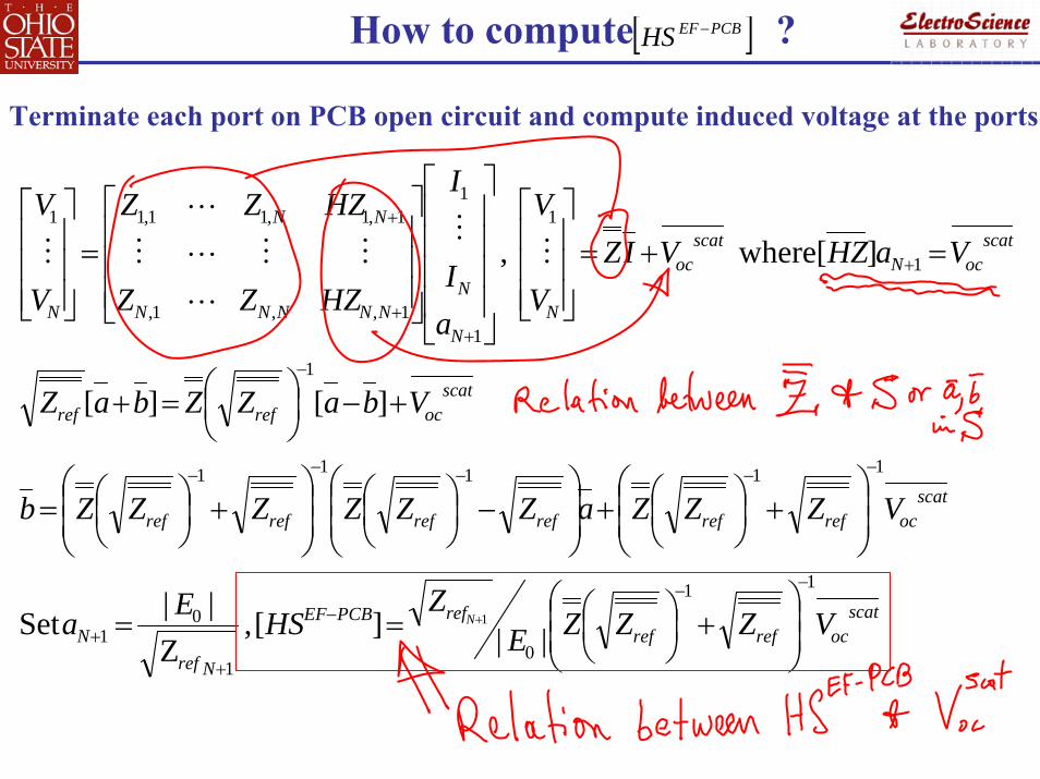
How to compute ?[ ]PCBEFHS −
Terminate each port on PCB open circuit and compute induced voltage at the ports.
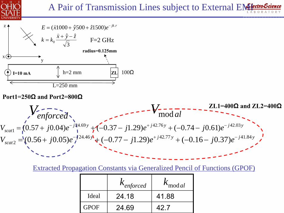
ZLI=10 mA
y
z
x
h=2 mm
L=250 mm
radius=0.125mm
F=2 GHz3
ˆˆ)1500ˆ500ˆ1000(
0
.
zyxkk
ezyxE rjk
−+=
++= −
)
)
100Ω
A Pair of Transmission Lines subject to External EMI
Port1=250Ω and Port2=800ΩZL1=400Ω and ZL2=400Ω
enforcedV alVmod
Extracted Propagation Constants via Generalized Pencil of Functions (GPOF)
Ideal 24.18 41.88GPOF 24.69 42.7
enforcedk alkmod
yjyjyjscat ejejejV 03.4276.4269.24
1 )61.074.0()29.137.0()04.057.0( −+− −−+−−++=yjyjyj
scat ejejejV 84.4177.4246.242 )37.016.0()29.177.0()05.056.0( −+− −−+−−++=
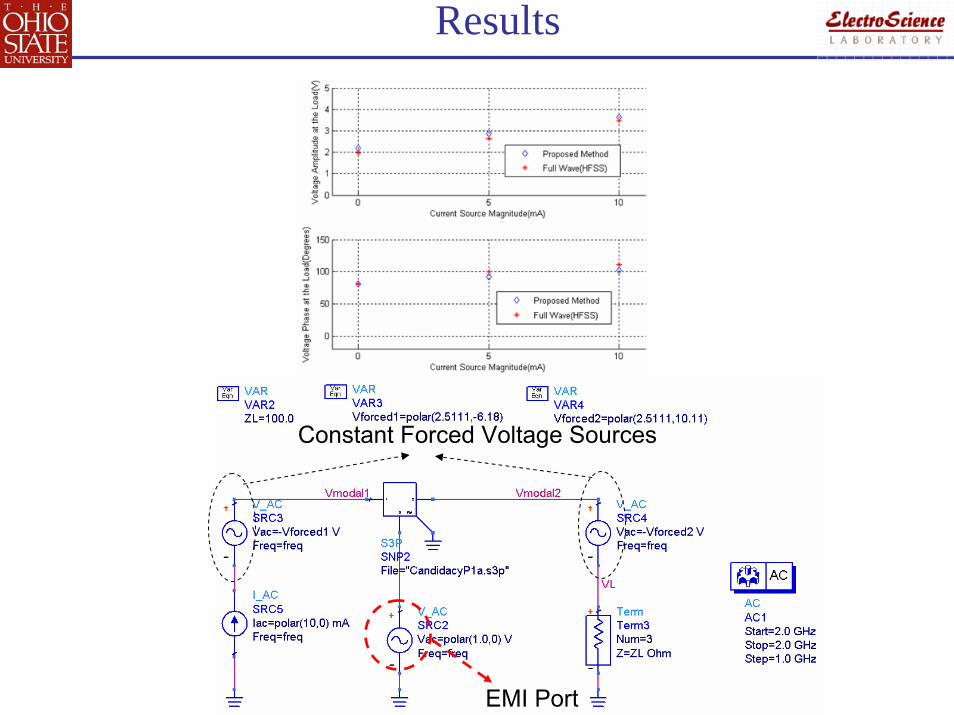
EMI Port
Results
Constant Forced Voltage Sources
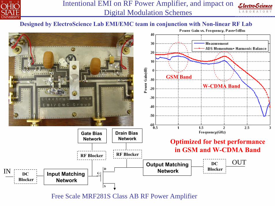
Intentional EMI on RF Power Amplifier, and impact on Digital Modulation Schemes
Free Scale MRF281S Class AB RF Power Amplifier
GSM Band
W-CDMA Band
Input MatchingNetwork
D
S
G
Gate Bias Network
Drain Bias Network
Output MatchingNetwork
RF Blocker RF Blocker
DCBlocker
DCBlockerIN
OUT
Designed by ElectroScience Lab EMI/EMC team in conjunction with Non-linear RF Lab
Optimized for best performancein GSM and W-CDMA Band
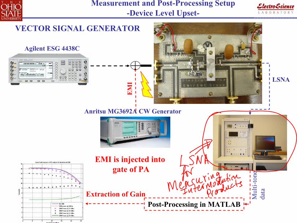
Agilent ESG 4438C
Anritsu MG3692A CW Generator
EM
I
Measurement and Post-Processing Setup-Device Level Upset-
VECTOR SIGNAL GENERATOR
Post-Processing in MATLAB
Mul
ti-to
neda
ta
LSNA
EMI is injected into gate of PA
Extraction of Gain
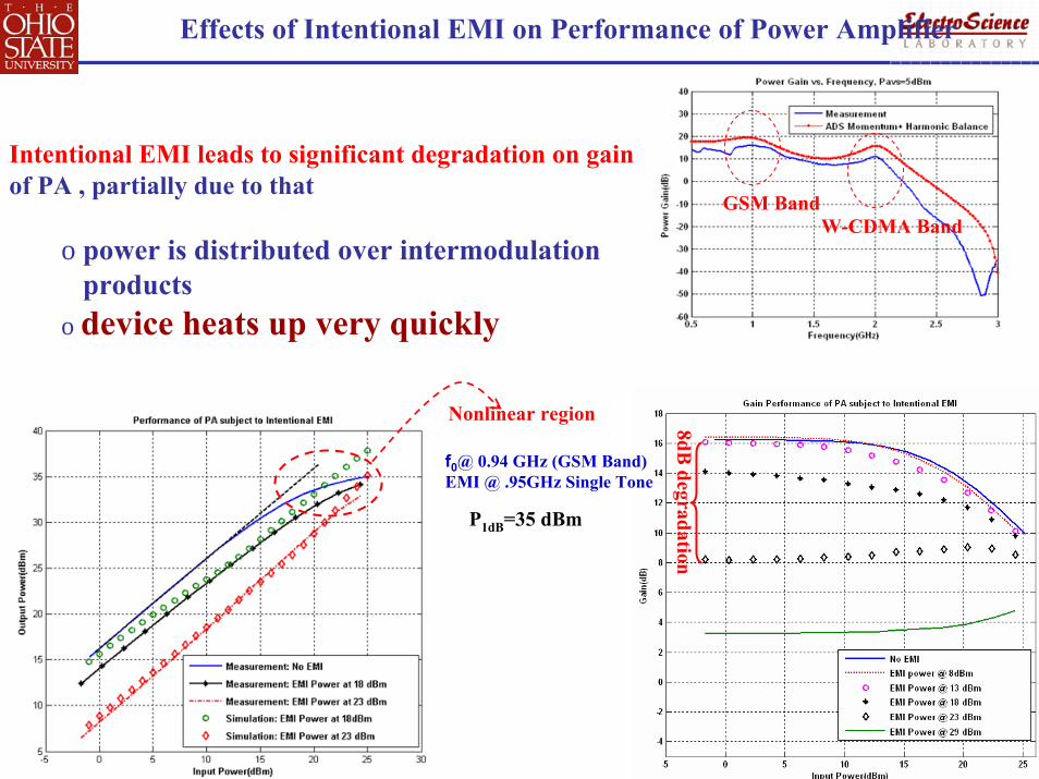
GSM BandW-CDMA Band
f0@ 0.94 GHz (GSM Band)EMI @ .95GHz Single Tone
Nonlinear region
P1dB=35 dBm
8dB degradation
Effects of Intentional EMI on Performance of Power Amplifier
Intentional EMI leads to significant degradation on gainof PA , partially due to that
o power is distributed over intermodulation products
o device heats up very quickly
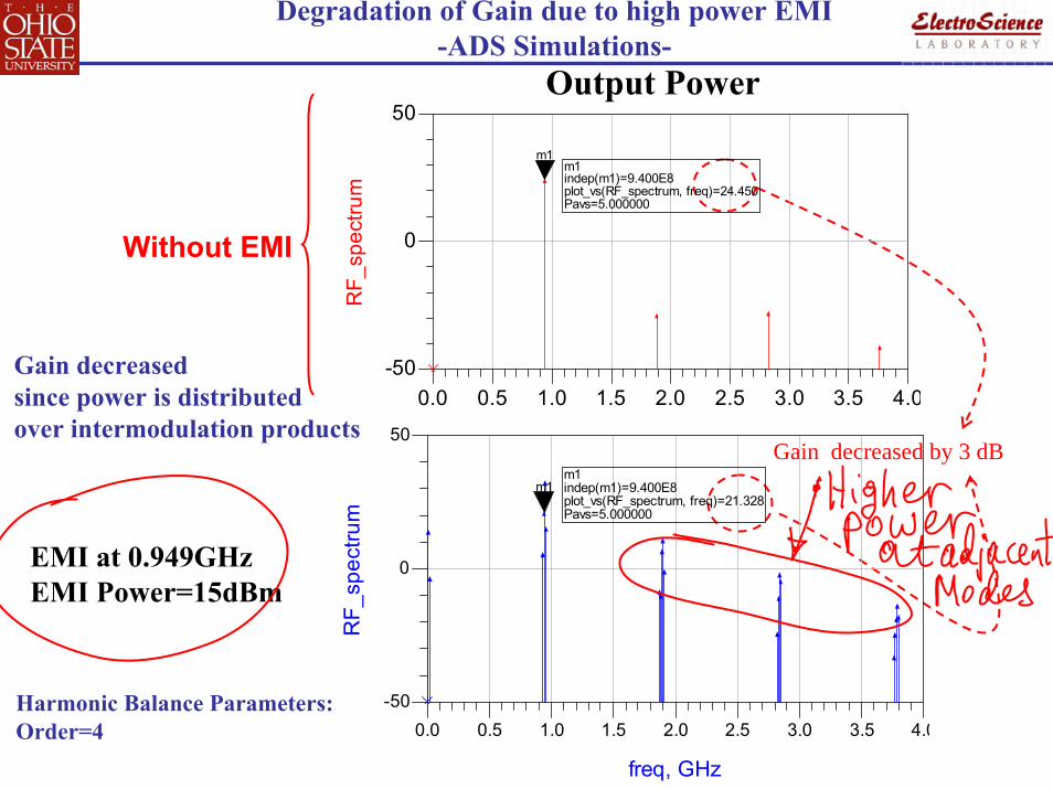
EMI at 0.949GHzEMI Power=15dBm
Harmonic Balance Parameters:Order=4
Gain decreased by 3 dB
Without EMI
Degradation of Gain due to high power EMI-ADS Simulations-
Output Power
0.5 1.0 1.5 2.0 2.5 3.0 3.50.0 4.0
0
-50
50
RF_
spec
trum
m1m1indep(m1)=plot_vs(RF_spectrum, freq)=24.450Pavs=5.000000
9.400E8
0.5 1.0 1.5 2.0 2.5 3.0 3.50.0 4.0
0
-50
50
freq, GHz
RF_
spec
trum
m1m1indep(m1)=plot_vs(RF_spectrum, freq)=21.328Pavs=5.000000
9.400E8
Gain decreased since power is distributed over intermodulation products
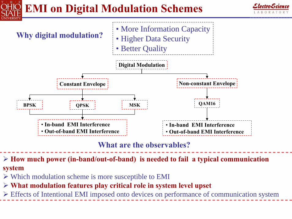
EMI on Digital Modulation Schemes
Digital Modulation
Constant Envelope Non-constant Envelope
• In-band EMI Interference• Out-of-band EMI Interference
QPSKBPSK MSK
• In-band EMI Interference• Out-of-band EMI Interference
QAM16
Why digital modulation?• More Information Capacity• Higher Data Security• Better Quality
What are the observables?
How much power (in-band/out-of-band) is needed to fail a typical communication system
Which modulation scheme is more susceptible to EMIWhat modulation features play critical role in system level upsetEffects of Intentional EMI imposed onto devices on performance of communication system
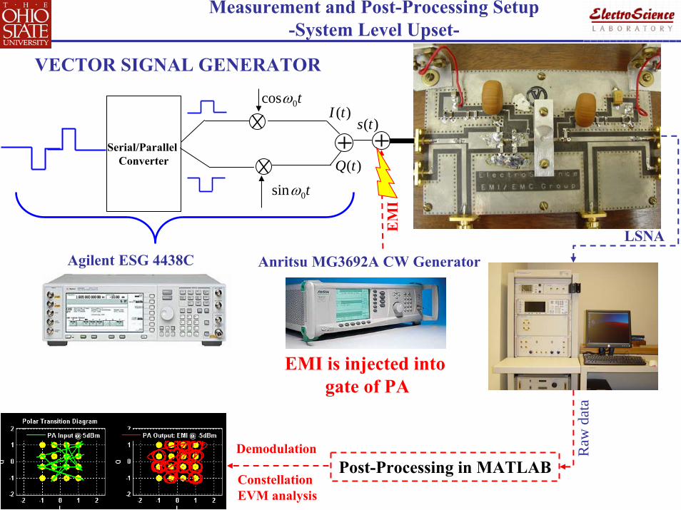
Agilent ESG 4438C Anritsu MG3692A CW Generator
Serial/Parallel Converter
t0cosω
t0sinω
)(tI
)(tQ
)(ts
EM
I
Measurement and Post-Processing Setup-System Level Upset-
VECTOR SIGNAL GENERATOR
Post-Processing in MATLAB
Raw
dat
a
LSNA
Demodulation
ConstellationEVM analysis
EMI is injected into gate of PA
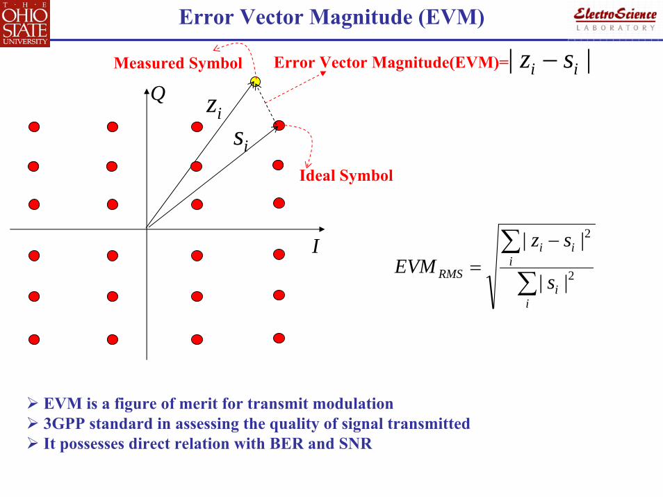
Error Vector Magnitude (EVM)
I
Q
Ideal Symbol
Measured Symbol Error Vector Magnitude(EVM)=
isiz
|| ii sz −
∑∑ −
=
ii
iii
RMS s
szEVM 2
2
||
||
EVM is a figure of merit for transmit modulation3GPP standard in assessing the quality of signal transmittedIt possesses direct relation with BER and SNR
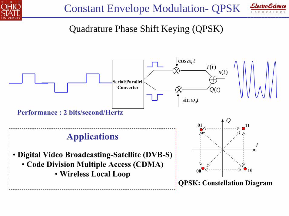
Constant Envelope Modulation- QPSK
QPSK: Constellation Diagram
I
Q11
10
01
00
Quadrature Phase Shift Keying (QPSK)
Applications
• Digital Video Broadcasting-Satellite (DVB-S)• Code Division Multiple Access (CDMA)
• Wireless Local Loop
Serial/Parallel Converter
t0cosω
t0sinω
)(tI
)(tQ
)(ts
Performance : 2 bits/second/Hertz
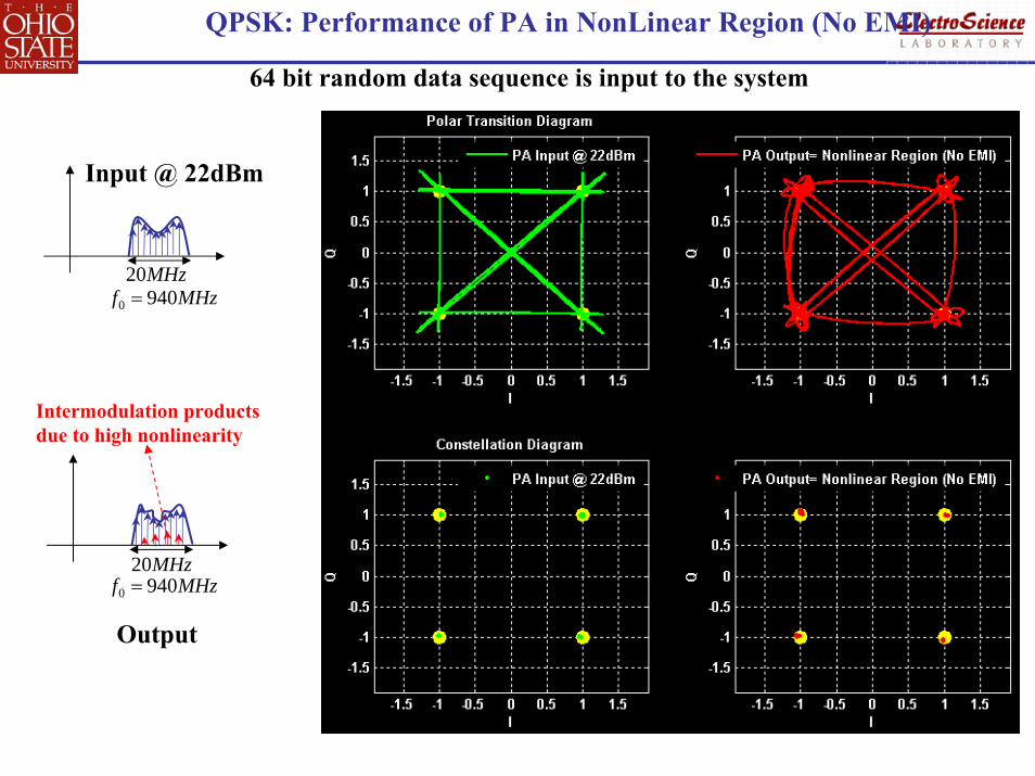
QPSK: Performance of PA in NonLinear Region (No EMI)
MHzf 9400 =
Input @ 22dBm
MHzf 9400 =
Output
Intermodulation products due to high nonlinearity
MHz20
MHz20
64 bit random data sequence is input to the system
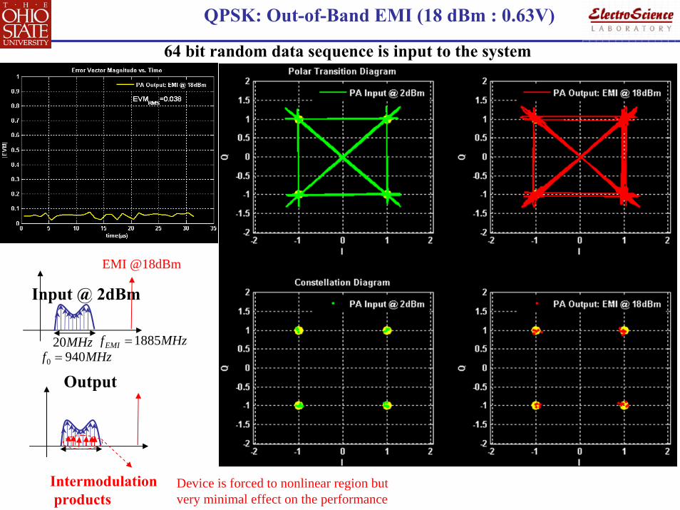
MHzf 9400 =
Input @ 2dBm
MHz20
EMI @18dBm
QPSK: Out-of-Band EMI (18 dBm : 0.63V)
Output
Device is forced to nonlinear region but very minimal effect on the performance
MHzfEMI 1885=
Intermodulationproducts
64 bit random data sequence is input to the system
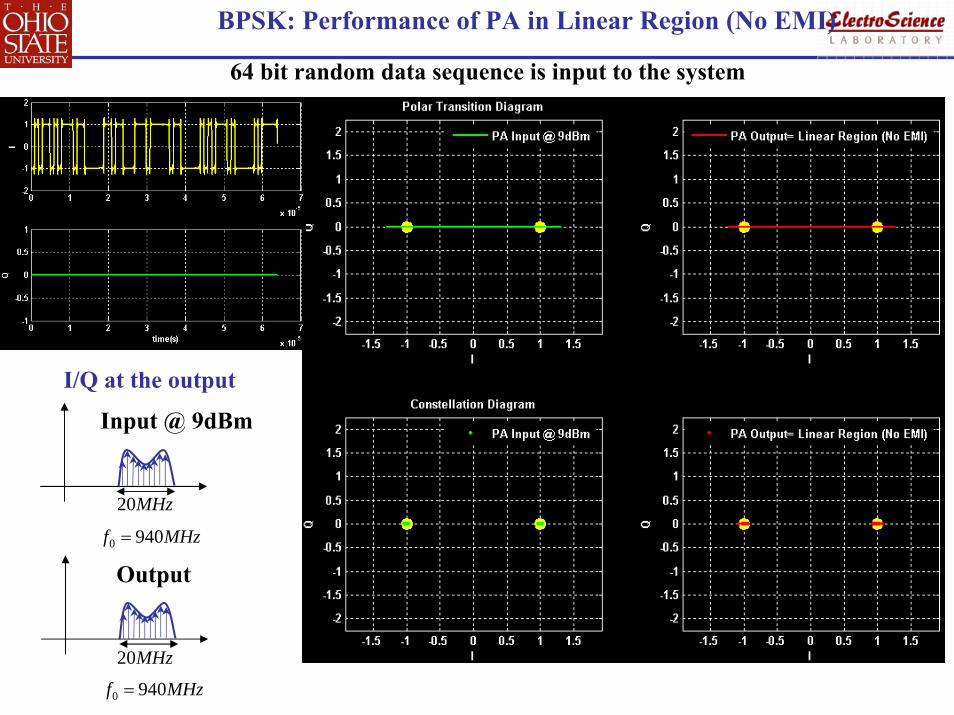
BPSK: Performance of PA in Linear Region (No EMI)
I/Q at the output
64 bit random data sequence is input to the system
MHzf 9400 =
Input @ 9dBm
MHzf 9400 =
Output
MHz20
MHz20
MHzf 9400 =
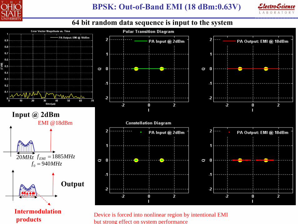
Input @ 2dBm
MHz20
EMI @18dBm
BPSK: Out-of-Band EMI (18 dBm:0.63V)
Output
MHzfEMI 1885=
Intermodulationproducts
64 bit random data sequence is input to the system
Device is forced into nonlinear region by intentional EMI but strong effect on system performance
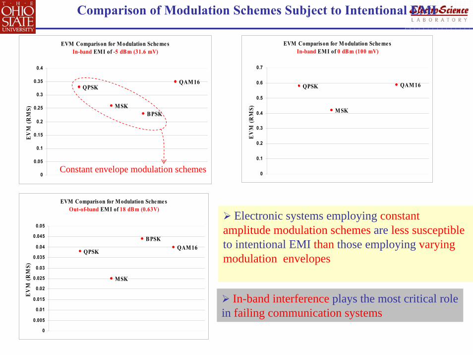
EVM Comparison for Modulation Sche me sIn-band EMI of -5 dBm (31.6 mV)
MSKBPSK
QAM16QPSK
0
0.05
0.1
0.15
0.2
0.25
0.3
0.35
0.4
EV
M (R
MS)
EVM Comparison for Modulation Sche me sIn-band EMI of 0 dBm (100 mV)
QPSK
MSK
QAM16
0
0.1
0.2
0.3
0.4
0.5
0.6
0.7
EV
M (R
MS)
EVM Comparison for Modulation SchemesOut-of-band EMI of 18 dBm (0.63V)
QPSK
MSK
BPSKQAM16
0
0.005
0.01
0.015
0.02
0.025
0.03
0.035
0.04
0.045
0.05
EV
M (R
MS)
Electronic systems employing constant amplitude modulation schemes are less susceptibleto intentional EMI than those employing varying modulation envelopes
Comparison of Modulation Schemes Subject to Intentional EMI
Constant envelope modulation schemes
In-band interference plays the most critical role in failing communication systems
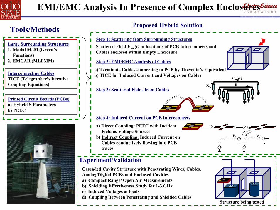
Step 1: Scattering from Surrounding Structures
Step 2: EMI/EMC Analysis of Cables
Step 3: Scattered Fields from Cables
Step 4: Induced Current on PCB Interconnects
EMI/EMC Analysis In Presence of Complex Enclosures
Cascaded Cavity Structure with Penetrating Wires, Cables, Analog/Digital PCBs and Enclosed Cavitiesa) Compact Range/ Open Air Measurementsb) Shielding Effectiveness Study for 1-3 GHzc) Induced Voltages at loadsd) Coupling Between Penetrating and Shielded Cables
Tools/Methods
Printed Circuit Boards (PCBs) a) Hybrid S Parametersb) PEEC
Large Surrounding Structures1. Modal MoM (Green’s
Functions)2. EMCAR (MLFMM)
Interconnecting CablesTICE (Telegrapher’s IterativeCoupling Equations)
Proposed Hybrid Solution
Experiment/Validation
Scattered Field Einc(r) at locations of PCB Interconnects and Cables enclosed within Empty Enclosure
Eapt(r)
Zth
a) Terminate Cables connecting to PCB by Thevenin’s Equivalentb) TICE for Induced Current and Voltages on Cables
+-
+-
+-
+-
Vs Vs
a) Direct Coupling: PEEC with Incident Field as Voltage Sources
b) Indirect Coupling: Induced Current on Cables conductively flowing into PCB traces
Structure being tested
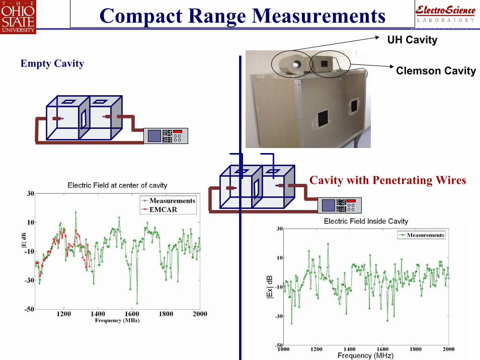
Compact Range Measurements
Empty Cavity
Cavity with Penetrating Wires
UH Cavity
Clemson Cavity
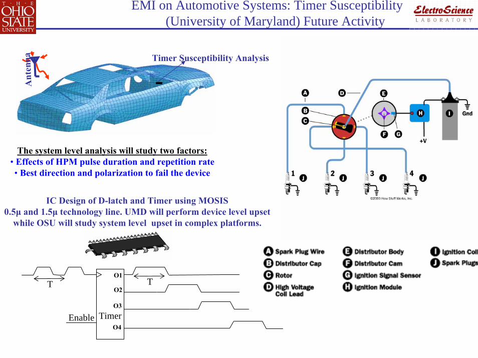
Timer
Timer Susceptibility Analysis
Ant
enna
The system level analysis will study two factors:
EMI on Automotive Systems: Timer Susceptibility(University of Maryland) Future Activity
• Effects of HPM pulse duration and repetition rate• Best direction and polarization to fail the device
IC Design of D-latch and Timer using MOSIS0.5μ and 1.5μ technology line. UMD will perform device level upset
while OSU will study system level upset in complex platforms.
T
Enable
TO1
O2
O3
O4