Embed Size (px)
DESCRIPTION
Magazine for Research, Innovation and Technology Transfer - Volume 9, Issue 32
Citation preview
Anniversaries for the keys to the nanoworld 06
Plasma technology for the textile industry 18
“Detectives” investigatefaulty electronics 20
Magazine for Research, Innovation and Technology TransferVolume 9 / Issue 32 / February 2011
EmpaNews
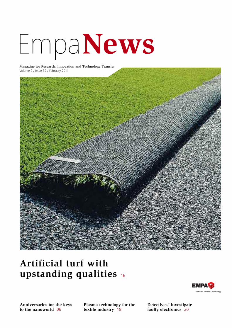
Artificial turf with upstanding qualities 16
02 // Editorial
Microscopes & Nobel PrizesAnniversaries for the keys to the nanoworld 06
There’s no suchthing as “zero risk”
Nanotechnology – or, to be precise, nanotech-nologies – have good cause to celebrate. Thisyear marks the 30th anniversary of the scanning
tunnelling microscope. This instrument and others likeit enable us to peer into the world of atoms and molecules
and thus make it accessible to us. Mean-while, thanks to nanoeffects, numerousmaterials and products have been devel-oped – and even brought to market – withnew, very promising properties.
As always, when humankind is con-fronted with new technologies, some peoplesee the glass as half full while others see itas half empty. When navigating these tech-nological crosscurrents, we must deal with
“nano” in a responsible manner. We do so by recognisingand minimising possible risks at an early stage, without atthe same time squandering the enormous opportunities itpresents such as in the areas of energy or the environment.
The demand for “risk free” actions, arising time andagain out of a mindset which pretends we can protect our-selves against every possible eventuality, is of little helphere. Risks have simply belonged to our very existencefrom time immemorial. They’re an essential part of the“background noise” that accompanies every change, be-cause anyone who dares to chart a new and unknowncourse takes on risk.
New technologies can turn our lives completely up-side down in a positive way. Just think about the intro-duction of the automobile or the Internet. In such situ -ations, we must weigh the costs – in this context, the poten-tial risks – against the expected benefits, and do so ration-ally while considering all the facts available to us.
In the area of nanotechnologies, things are moving fastin Switzerland at the moment. For instance, the NationalResearch Programme “Opportunities and Risks of Nano-materials” has just started up, and Empa researchers areheavily involved in it. Further, the Swiss NanoConvention,with Empa as one of its organisers, will take place in Mayin Baden, and its goal is to intensify and expand the inter-disciplinary dialogue on the topic of all things “nano”.
Enjoy your reading!
Michael HagmannHead Communications
Cover
Empa researchers, together with the Swiss company TISCA TIARA, have developeda bi-component fibre for a novel type of artificial turf, one which thanks to its hardenedcore always returns to an upright position and because of its soft sheath avoids abrasions and grass burns. (Photo: TISCA TIARA)
Table of contents // 03
Cause & effect“Detectives” investigate faulty electronics 20
Comfort & environmentPlasma technology for the textile industry 18
Chemical reactions & analysesSTM and AFM today 10
Research and development
04 The art of insulating
Focus: nanotechnology and its instruments
06 Gate to the nanoworld
08 Research Programme set into motion
10 Happy Birthday!
13 Chemistry with electron beams
Knowledge and technology transfer
16 Artificial turf with upstanding qualities
18 Adapted to industry
Services20 Debugging – successfully completed
Science dialogue22 Swiss Innovation Forum 2010
23 Technology Days 2010
24 Events
Imprint
PublisherEmpaÜberlandstrasse 129CH-8600 DübendorfSwitzerlandwww.empa.ch
Text & DesignCommunication section
ContactPhone +41 44 823 47 [email protected]
Published quarterly
ISSN 1662-7768
04 // Research and development
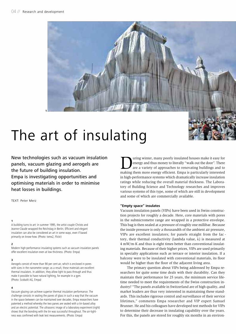
During winter, many poorly insulated houses make it easy forenergy and thus money to literally “walk out the door”. Thereare a variety of approaches to renovating buildings and to
making them more energy efficient. Empa is particularly interestedin high-performance systems which dramatically increase insulationratings while reducing the overall material thickness. The Labora -tory of Building Science and Technology researches and improvesvarious systems of this type, some of which are still in developmentand some of which are commercially available.
“Empty space” insulatesVacuum insulation panels (VIPs) have been used in Swiss construc-tion projects for roughly a decade. Here, core materials with poresin the submicrometre range are wrapped in a protective envelope.This bag is then sealed at a pressure of roughly one millibar. Becausethe inside pressure is only a thousandth of the ambient air pressure,VIPs are excellent insulators; for panels straight from the fac -tory, their thermal conductivity (lambda value, l) is measured at4 mW/m.K and thus is eight times better than conventional insulat-ing materials. Because of their higher prices, VIPs are used primarilyin specialty applications such as terrace or interior insulation. If abalcony were to be insulated with conventional materials, its floorwould be higher than the floor of the adjacent living area.
The primary question about VIPs being addressed by Empa re-searchers for quite some time deals with their durability. Can theymaintain their performance for 25 years, the minimum service life-time needed to meet the requirements of the Swiss construction in-dustry? “The panels available in Switzerland are of high quality, andmarket leaders are thus very interested in maintaining these stand -ards. This includes rigorous control and surveillance of their servicelifetimes,” comments Empa researcher and VIP expert SamuelBrunner. He and his colleagues have developed test methods for VIPsto determine their decrease in insulating capability over the years.For this, the panels are stored for roughly six months in an environ-
New technologies such as vacuum insulationpanels, vacuum glazing and aerogels are the future of building insulation. Empa is investigating opportunities and optimising materials in order to minimiseheat losses in buildings.
TEXT: Peter Merz
The art of insulating
1
1A building turns to art: in summer 1995, the artist couple Christo and Jeanne-Claude wrapped the Reichstag in Berlin. Efficient and elegant insulation can also be considered an art in some ways, even if based primarily on know-how. (Photo: txmx2, Flickr)
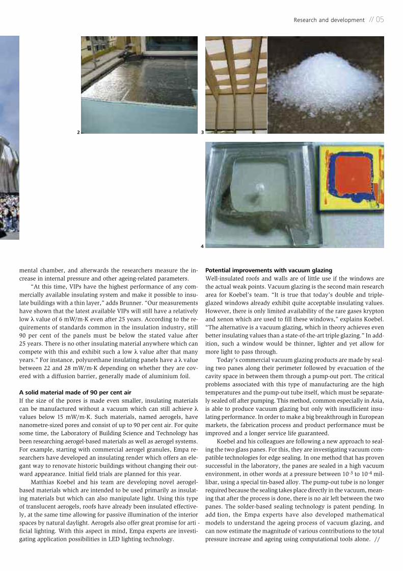
2Modern high-performance insulating systems such as vacuum insulation panelsoffer excellent insulation even at low thickness. (Photo: Empa)
3Aerogels consist of more than 90 per cent air, which is enclosed in pores with sizes in the nanometre range; as a result, these materials are excellent thermal insulators. In addition, they allow light to pass through and thus make it possible to have natural lighting, for example in a gym. (Photo: Scobalit AG, Empa)
4Vacuum glazing can achieve superior thermal insulation performance. The challenge consists in sealing the panes of glass in such a way that the vacuumin the space between can be maintained over decades. Empa researchers havepatented a method whereby the two panes are sealed with a tin-based alloyand an electric potential. The ultrasonic image of a laboratory experiment (right)shows that the bonding with the tin was successful throughout. The air-tight-ness was confirmed with leak test measurements. (Photo: Empa)
Research and development // 05
mental chamber, and afterwards the researchers measure the in-crease in internal pressure and other ageing-related parameters.
“At this time, VIPs have the highest performance of any com-mercially available insulating system and make it possible to insu-late buildings with a thin layer,” adds Brunner. “Our measurementshave shown that the latest available VIPs will still have a relativelylow l value of 6 mW/m.K even after 25 years. According to the re-quirements of standards common in the insulation industry, still90 per cent of the panels must be below the stated value after 25 years. There is no other insulating material anywhere which cancompete with this and exhibit such a low l value after that manyyears.” For instance, polyurethane insulating panels have a l valuebetween 22 and 28 mW/m.K depending on whether they are cov-ered with a diffusion barrier, generally made of aluminium foil.
A solid material made of 90 per cent airIf the size of the pores is made even smaller, insulating materialscan be manufactured without a vacuum which can still achieve lvalues below 15 mW/m.K. Such materials, named aerogels, havenanometre-sized pores and consist of up to 90 per cent air. For quitesome time, the Laboratory of Building Science and Technology hasbeen researching aerogel-based materials as well as aerogel systems.For example, starting with commercial aerogel granules, Empa re-searchers have developed an insulating render which offers an ele -gant way to renovate historic buildings without changing their out-ward appearance. Initial field trials are planned for this year.
Matthias Koebel and his team are developing novel aerogel-based materials which are intended to be used primarily as insulat-ing materials but which can also manipulate light. Using this typeof translucent aerogels, roofs have already been insulated effective-ly, at the same time allowing for passive illumination of the interiorspaces by natural daylight. Aerogels also offer great promise for arti -ficial lighting. With this aspect in mind, Empa experts are investi-gating application possibilities in LED lighting technology.
Potential improvements with vacuum glazingWell-insulated roofs and walls are of little use if the windows arethe actual weak points. Vacuum glazing is the second main researcharea for Koebel’s team. “It is true that today’s double and triple-glazed windows already exhibit quite acceptable insulating values.However, there is only limited availability of the rare gases kryptonand xenon which are used to fill these windows,” explains Koebel.“The alternative is a vacuum glazing, which in theory achieves evenbetter insulating values than a state-of-the-art triple glazing.” In add -ition, such a window would be thinner, lighter and yet allow formore light to pass through.
Today’s commercial vacuum glazing products are made by seal-ing two panes along their perimeter followed by evacuation of thecavity space in between them through a pump-out port. The criticalproblems associated with this type of manufacturing are the hightemperatures and the pump-out tube itself, which must be separate-ly sealed off after pumping. This method, common especially in Asia,is able to produce vacuum glazing but only with insufficient insu-lating performance. In order to make a big breakthrough in Europeanmarkets, the fabrication process and product performance must beimproved and a longer service life guaranteed.
Koebel and his colleagues are following a new approach to seal-ing the two glass panes. For this, they are investigating vacuum com-patible technologies for edge sealing. In one method that has provensuccessful in the laboratory, the panes are sealed in a high vacuumenvironment, in other words at a pressure between 10-3 to 10-4 mil-libar, using a special tin-based alloy. The pump-out tube is no longerrequired because the sealing takes place directly in the vacuum, mean-ing that after the process is done, there is no air left between the twopanes. The solder-based sealing technology is patent pending. Inadd ition, the Empa experts have also developed mathematicalmodels to understand the ageing process of vacuum glazing, andcan now estimate the magnitude of various contributions to the totalpressure increase and ageing using computational tools alone. //
32
4
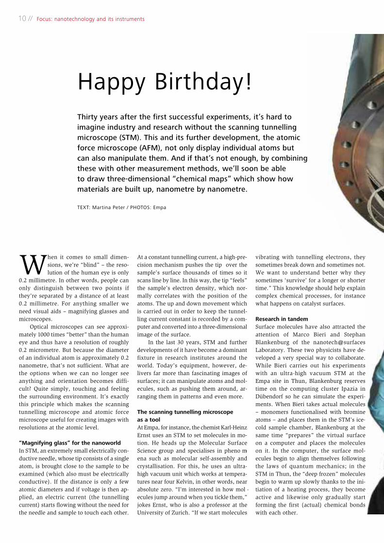
Gate to the nanoworld30 years ago, Heinrich Rohrer and Gerd Binnig at the IBM Research Laboratory in Rüschlikon, just outside of Zurich, were the first to successfully construct ascanning tunnelling microscope – a feat for which they were awarded the NobelPrize for Physics just five years later. This development is considered one of thecrucial steps leading towards nanotechnology, our access to individual moleculesand atoms and thus the basic building blocks of all matter.
TEXT: Beatrice Huber / PHOTO: Empa
Nanotechnology as we know it today would not even existwithout the instruments that allow us to peer into the worldof the infinitesimal so we can analyse and manipulate it.
Scientists at Empa use equipment such as electron microscopes,scanning tunnelling microscopes and atomic force microscopes fortheir research, and are also expanding the areas in which these toolscan be used, as the articles on the following pages illustrate. Thisyear, the scanning tunnelling microscope is celebrating its 30th
birthday. In 1981, Heinrich Rohrer and Gerd Binnig at the IBM Re-search Laboratory in Rüschlikon developed the first instrument ofthis type which had the necessary precision and stability. Just a fewyears later in 1986, their work was honoured with the Nobel Prizein Physics.
A microscope which scans the surfaceThe scanning tunnelling microscope isn’t a “real” microscope be-cause it doesn’t generate a direct optical image of the object beingexamined. Instead, the instrument examines the profile of a surfacewith a scanning tip whereby there’s always a tiny distance betweenthe tip and the surface. This prevents anything from being damagedduring the scanning process. For its measurements, the microscopeuses what is known as the quantum tunnelling effect. This quan-tum-mechanical effect, which gives the microscope its name, allowsan electron (or some other particle) to drill a tunnel through a po-tential barrier which, according to classical physics, would be im-penetrable. This movement of electrons creates a measurable cur-rent despite the fact that the scanning tip and the surface don’t makecontact. Flash memories, such as the chips in USB sticks, are alsobased on the tunnelling effect.
In 1986, Rohrer and Binnig shared the Nobel Prize in Physicswith the German electrical engineer Ernst Ruska, who had alreadydeveloped the electron microscope in the 1930s. Instead of normallight, that instrument uses an electron beam and with it achievesconsiderably higher resolution. Traditional optical microscopeshave a resolution of approximately 200 nanometres, whereas thesedays electron microscopes have increased this to approximately0.1 nano metre. Just like scanning tunnelling microscopes, electronmicroscopes have also long since become indispensable tools innano technology. //
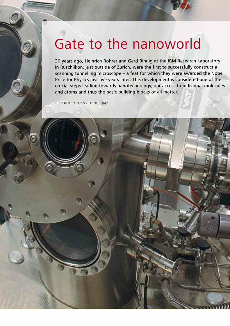
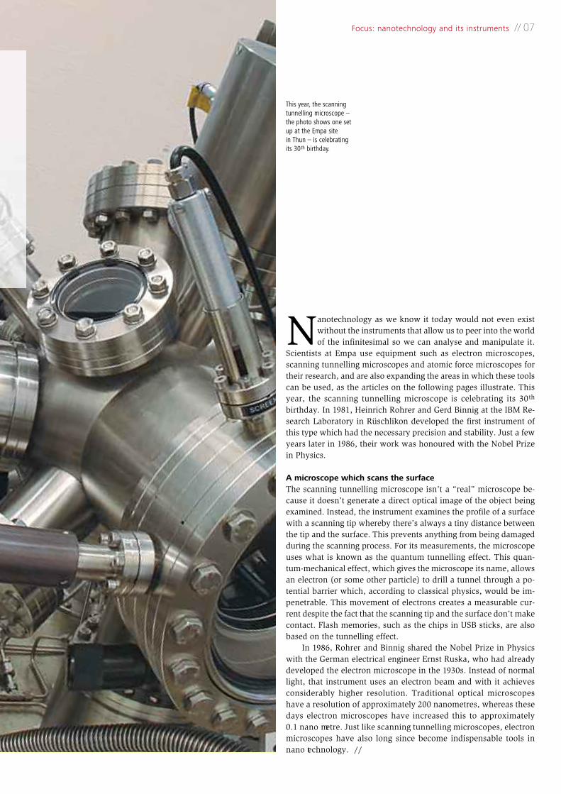
This year, the scanning tunnelling microscope – the photo shows one set up at the Empa site in Thun – is celebrating its 30th birthday.
Focus: nanotechnology and its instruments // 07
08 // Focus: nanotechnology and its instruments
Research Programmeset into motionWhat opportunities do nanomaterials offer, and which risks do they entail? The National Research Programme NRP 64 intends to fill in existing gaps in knowledge and in this way contribute to the long-term success of nanomaterials. Empa is participating in four of the 17 sponsored projects.
TEXT: Beatrice Huber
Information technology, electronics, construction materials, environmental technol -ogy, energy technology, household appliances, textiles, cosmetics, foodstuffs, medicine– there’s practically no limit to where nanomaterials can be put to use. Around the
world there are already more than a thousand products on the market which contain nano-materials. In the area of nanosciences, Swiss research institutes, including Empa, areamong the world leaders. Nanomaterials offer enormous opportunities for Switzerland asa location for research and industrial applications. Their economic success, however, canonly be long-term if possible risks can also be evaluated in a reliable manner.
Exploring opportunities and risksThe projects which are part of the recently initiated National Research Programme “Op-portunities and Risks of Nanomaterials” (NRP 64) should therefore not only explore theopportunities which nanomaterials offer towards improving our health, environment anduse of natural resources but also possible risks. Within an NRP, researchers from variousdisciplines collaborate on projects which are intended to contribute to the solutions of keypresent-day problems. The Swiss Federal Council sets the focus; the NRPs are carried outby the Swiss National Science Foundation (SNSF).
NRP 64 places its focus on synthetically manufactured nanomaterials. A “nanoma -terial” is considered one which has structural components with at least one dimension ofless than 100 nanometres. In this programme, especially those materials will be examinedwhere there is a high probability of human or environmental exposure. One of the goalsof NRP 64 is also to create the basis for developing tools to monitor and evaluate the effectsof nanomaterials on people and the environment.
At the end of November 2010, the SNSF approved 17 project proposals from the 44 whichwere submitted, and is financing them for the first three years with CHF 6.3 million. Emparesearchers are heading up three of these projects and are participating in yet another. //
Is nano sustainable in the long run?
In order to master challengessuch as climate change or short-ages of natural resources, weneed long-term solutions. Nano -technologies and nanomaterialscan provide new approaches.The Swiss Academy of Engineer-ing Sciences (SATW), along withleading Swiss nano experts suchas Pierangelo Gröning, a mem-ber of Empa’s Board of Direc-tors, has published a brochureaddressing long-term sustain-ability and nanotechnology. Italso calls for a public discussionabout the associated opportu n -ities and risks. That’s becausenanotechnologies will enjoysuccess over the long term andmake a contribution to sustain-able development only if theydo not entail any major risks.This brochure (in German) canbe downloaded in PDF format atwww.satw.ch/nano.
Focus: nanotechnology and its instruments // 09
How nanotechnologies will impact our future
In order to develop innovative technologies efficiently, as well as to finance and regulate them, sounddecisions must be taken which are based on the latest knowledge and findings. This is also the casewith nanotechnology. The Swiss NanoConvention 2011 supports decision-makers in this role. It of-fers a platform where leaders from research and industry, key figures in innovation and technology,entrepreneurs, investors as well as administrators and politicians can gather to discuss ideas andexchange viewpoints – or even develop new ones. The participants will receive in-depthinformation about one of the most important emerging technologies of the 21st centuryand its potential for innovative approaches, products and services. In parallel to theSwiss NanoConvention, the NanoPubli event is inviting the general public to be-come informed about the world of the extremely small, first-hand at an exhibitionand during lectures.The central topics of the event are the major challenges of our time such as secur-
ing a sustainable energy supply and a clean environment along with the future of med-icine with nano-therapeutics and diagnostics plus the development of innovative functionalmaterials and their numerous industrial applications. Another focus will be the potential risks asso-ciated with free nanoparticles along with how society sees and addresses these issues.In short, the Swiss NanoConvention is the showplace for nanotechnology in Switzerland. Because
it is being organised jointly by the “who’s who” of the Swiss nano community, it’s the ideal place toget to know the leading minds and foremost proponents of nanotechnology.Further information, including the programme and registration, is available at www.swissnanoconvention.ch
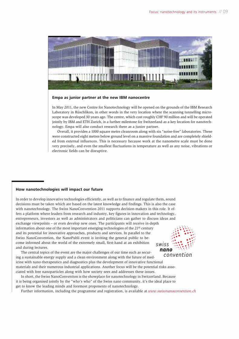
Empa as junior partner at the new IBM nanocentre
In May 2011, the new Centre for Nanotechnology will be opened on the grounds of the IBM ResearchLaboratory in Rüschlikon, in other words in the very location where the scanning tunnelling micro-scope was developed 30 years ago. The centre, which cost roughly CHF 90 million and will be operatedjointly by IBM and ETH Zurich, is a further milestone for Switzerland as a key location for nanotech-nology. Empa will also conduct research there as a junior partner.Overall, it provides a 1000 square metre cleanroom along with six “noise-free” laboratories. These
were constructed eight metres below ground level on a massive foundation and are completely shield-ed from external influences. This is necessary because work at the nanometre scale must be donevery precisely, and even the smallest fluctuations in temperature as well as any noise, vibrations orelectronic fields can be disruptive.
Photo: IBM
10 // Focus: nanotechnology and its instruments
Happy Birthday!Thirty years after the first successful experiments, it’s hard to imagine industry and research without the scanning tunnelling microscope (STM). This and its further development, the atomicforce microscope (AFM), not only display individual atoms but can also manipulate them. And if that’s not enough, by combiningthese with other measurement methods, we’ll soon be able to draw three-dimensional “chemical maps” which show how materials are built up, nanometre by nanometre.
TEXT: Martina Peter / PHOTOS: Empa
When it comes to small dimen-sions, we’re “blind” – the reso -lution of the human eye is only
0.2 millimetre. In other words, people canonly distinguish between two points ifthey’re separated by a distance of at least0.2 millimetre. For anything smaller weneed visual aids – magnifying glasses andmicroscopes.
Optical microscopes can see approxi-mately 1000 times “better” than the humaneye and thus have a resolution of roughly0.2 micrometre. But because the diameterof an individual atom is approximately 0.2nanometre, that’s not sufficient. What arethe options when we can no longer seeanything and orientation becomes diffi-cult? Quite simply, touching and feelingthe surrounding environment. It’s exactlythis principle which makes the scanningtunnelling microscope and atomic forcemicroscope useful for creating images withresolutions at the atomic level.
“Magnifying glass” for the nanoworldIn STM, an extremely small electrically con-ductive needle, whose tip consists of a singleatom, is brought close to the sample to beexamined (which also must be elec tricallyconductive). If the distance is only a fewatomic diameters and if voltage is then ap-plied, an electric current (the tunnellingcurrent) starts flowing without the need forthe needle and sample to touch each other.
At a constant tunnelling current, a high-pre-cision mechanism pushes the tip over thesample’s surface thousands of times so itscans line by line. In this way, the tip “feels”the sample’s electron density, which nor-mally correlates with the position of theatoms. The up and down movement whichis carried out in order to keep the tunnel -ling current constant is recorded by a com-puter and converted into a three-dimensionalimage of the surface.
In the last 30 years, STM and furtherdevelopments of it have become a dominantfixture in research institutes around theworld. Today’s equipment, however, de -livers far more than fascinating images ofsurfaces; it can manipulate atoms and mol-ecules, such as pushing them around, ar-ranging them in patterns and even more.
The scanning tunnelling microscope as a toolAt Empa, for instance, the chemist Karl-HeinzErnst uses an STM to set molecules in mo-tion. He heads up the Molecular SurfaceScience group and specialises in pheno m -ena such as molecular self-assembly andcrystallisation. For this, he uses an ultra-high vacuum unit which works at tempera-tures near four Kelvin, in other words, nearabsolute zero. “I’m interested in how mol -ecules jump around when you tickle them,”jokes Ernst, who is also a professor at theUniversity of Zurich. “If we start molecules
vibrating with tunnelling electrons, theysometimes break down and sometimes not.We want to understand better why theysometimes ‘survive’ for a longer or shortertime.” This knowledge should help explaincomplex chemical processes, for instancewhat happens on catalyst surfaces.
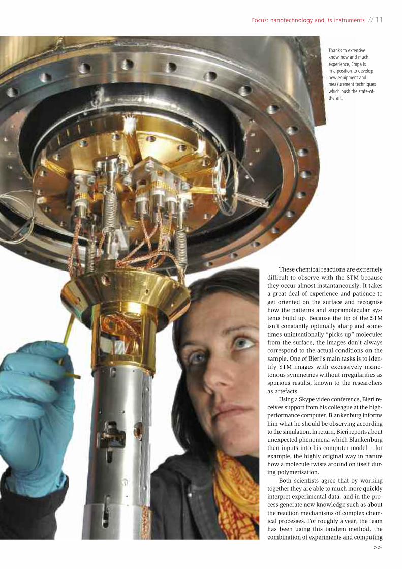
Research in tandemSurface molecules have also attracted theattention of Marco Bieri and StephanBlankenburg of the nanotech@surfacesLaboratory. These two physicists have de-veloped a very special way to collaborate.While Bieri carries out his experimentswith an ultra-high vacuum STM at theEmpa site in Thun, Blankenburg reservestime on the computing cluster Ipazia inDübendorf so he can simulate the experi-ments. When Bieri takes actual molecules– monomers functionalised with bromineatoms – and places them in the STM’s ice-cold sample chamber, Blankenburg at thesame time “prepares” the virtual surfaceon a computer and places the molecules on it. In the computer, the surface mol -ecules begin to align themselves followingthe laws of quantum mechanics; in theSTM in Thun, the “deep frozen” moleculesbegin to warm up slowly thanks to the ini-tiation of a heating process, they becomeactive and likewise only gradually startforming the first (actual) chemical bondswith each other.
Focus: nanotechnology and its instruments // 11
>>
H
Thanks to extensive know-how and much experience, Empa is in a position to develop new equipment and measurement techniqueswhich push the state-of-the-art.
These chemical reactions are extremelydifficult to observe with the STM becausethey occur almost instantaneously. It takesa great deal of experience and patience toget oriented on the surface and recognisehow the patterns and supramolecular sys-tems build up. Because the tip of the STMisn’t constantly optimally sharp and some-times unintentionally “picks up” moleculesfrom the surface, the images don’t alwayscorrespond to the actual conditions on thesample. One of Bieri’s main tasks is to iden-tify STM images with excessively mono -tonous symmetries without irregularities asspurious results, known to the researchersas artefacts.
Using a Skype video conference, Bieri re-ceives support from his colleague at the high-performance computer. Blankenburg informshim what he should be observing accordingto the simulation. In return, Bieri reports aboutunexpected phenomena which Blankenburgthen inputs into his computer model – forexample, the highly original way in naturehow a molecule twists around on itself dur-ing polymerisation.
Both scientists agree that by workingtogether they are able to much more quicklyinterpret experimental data, and in the pro -cess generate new knowledge such as aboutthe reaction mechanisms of complex chem-ical processes. For roughly a year, the teamhas been using this tandem method, thecombination of experiments and computing
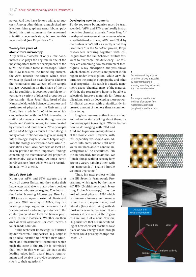
Developing new instrumentsTo do so, some boundaries must be tran-scended. “AFM and STM aren’t really instru-ments for chemical analysis,” notes Hug. “Ifwe deposit unknown atoms or molecules ona well-defined surface, AFM and STM bythemselves won’t tell us exactly what they‘see’ there.” In the NanoXAS project, Emparesearchers working together with col-leagues from the Paul Scherrer Institute thuswant to overcome this deficiency. For this,they are combining two measurement tech-niques: X-ray absorption analysis showswhich chemical elements are present in theregion under investigation, while AFM de-termines the sample’s topography and otherlocal properties. The result is a nearly nano -metre-exact “chemical map” of the material.With it, the researchers hope to be able toselectively improve materials for future ap-plications, such as developing more power-ful digital cameras with a significantly in-creased amount of memory than is common-place today.
Hug has numerous other ideas in mind,and when he starts talking about them, hispioneering spirit takes flight. “We’ve learnedhow to do imaging with STM andAFM and to perform manipulationsat the atomic level. However, withthis capability we should also ad-vance into areas where until nowwe’ve not been able to conduct in-vestigations,” he speculates. “Inthe nanoworld, for example, we‘touch’ things without sensing howstrongly we are handling them withour ‘nanohands’.” That’s a hurdlewe must overcome.”
Thus, his next project withinthe EU Seventh Framework Pro-gramme, which goes by the nameMDSPM (Multidimensional Scan-ning Probe Microscopy), has thegoal of developing an AFM whichcan measure forces simultaneous-ly vertically (perpendicular) andlaterally (from side to side) with al-most unbelievable precision. It re -cognises differences in the regionof a millionth of a nano-Newton.Hug surmises that our understand-ing of how chemical reactions takeplace or how energy is lost throughfriction could possibly change rad-ically. //
Photo diode Laser
SampleCantilever with tip
Detector andcontrol electronics
12 // Focus: nanotechnology and its instruments
>>
power. And they have done so with great suc-cess. Among other things, a much cited art -icle describing graphene nanoribbons, pub-lished this past summer in the renownedscientific magazine Nature, is based on thisnew method (see EmpaNews 31).
Twenty-five years of atomic force microscopyA tip with a diameter of only a few nano -metres also plays the key role in one of themost important further developments of theSTM, the atomic force microscope. Whilethe STM measures the tunnelling current,the AFM records the forces which arisewhen a tip placed on a cantilever is slid overthe “mountains and valleys” of the samplesurface. Depending on the shape of the tipand its condition, it becomes possible to in-vestigate a variety of physical properties onthe sample. Hans Josef Hug, head of theNanoscale Materials Science Laboratory andprofessor of physics at the University ofBasel, lists a whole “zoo” of forces whichcan be detected with the AFM: from electro-static and magnetic forces, through van derWaals and Casimir forces, to those createdby covalent and ionic bonds. “The principleof the AFM brings us much further along inmany areas: frictional forces give us insightinto tribology; magnetic forces help us opti-mise the storage of electronic data; while in-formation about local hardness or local ad-hesion provide us with important findingsconcerning the micromechanical propertiesof materials,” explains Hug. “At Empa there’shardly a single force which we can’t record,”he adds, with a wink.
Empa’s User LabNumerous AFM and STM experts are atwork all across Empa, and they make theirknowledge available to many others besidestheir own in-house colleagues. The doors tothe Swiss Scanning Microscopy User Lab(SUL) are also open to external clients andpartners. With an array of AFMs, they canin vestigate topologies and measure localfriction, as well as do in-depth studies of thecontact potential and local mechanical prop-erties of their materials. Whether on theirown or with assistance, for each there’s atailor-made solution.
“This technical knowledge is nurturedby our research,” emphasises Hug. Empa isin an ideal position to develop new equip-ment and measurement techniques whichpush the state-of-the-art. He is convincedthat “only in this way can we stay at theleading edge, fulfil users’ future require-ments and be able to provide competent an-swers to their questions.”
1Bromine-containing polymer on a silver surface, as revealedby experiments using a scanning tunnelling microscopeand computer simulations.
2The image shows the innerworkings of an atomic force microscope; a cantilever (see photo) scans the surface.
1
2
40µm
Focus: nanotechnology and its instruments // 13
Instruments such as electron microscopes, scanning tunnellingmicroscopes and atomic force microscopes have opened oureyes to the world of the infinitesimally small. They have for the
first time made it possible for those working in research and indus-try to fabricate targeted structures with nanometre feature sizes.However, these instruments can do much more. For instance, theelectron microscope can also be used for chemistry. In this case,suitable gas molecules are injected close to a sample which is al-ready in the microscope’s vacuum chamber. These adsorb on the
Chemistry with electron beamsFocussed electron beams are used in electron microscopes to allow us to see extremely small objects, and today such investigations have become routine. More recently, however, electron beams are being used for chemical reactions. For example, surface structures measuring only nanometres across can be “written”.Empa researchers are perfecting this technology and are searching for completelynew application areas.
TEXT: Beatrice Huber / PHOTOS: Empa
>>
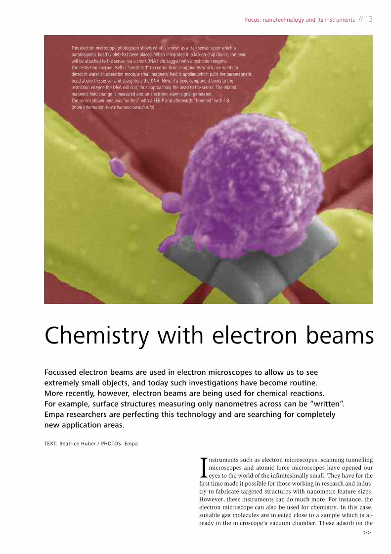
This electron microscope photograph shows what is known as a Hall sensor upon which a paramagnetic bead (violet) has been placed. When integrated in a lab-on-chip device, the bead will be attached to the sensor via a short DNA helix tagged with a restriction enzyme. The restriction enzyme itself is "sensitised" to certain toxic components which one wants to detect in water. In operation mode, a small magnetic field is applied which pulls the paramagnetic bead above the sensor and straightens the DNA. Now, if a toxic component binds to the restriction enzyme the DNA will curl, thus approaching the bead to the sensor. The related magnetic field change is measured and an electronic alarm signal generated. The sensor shown here was “written” with a FEBIP and afterwards “trimmed” with FIB. (more information www.bionano-switch.info)
14 // Focus: nanotechnology and its instruments
sample in a reversible manner. The focussed electron beam, whichnormally serves to make objects visible, now instead induceschemical reactions of the adsorbed gas molecules, but only at thespot where the beam strikes the surface. The resulting non-volatilemolecular fragments then remain permanently on the sample whilethe volatile fragments are removed by the vacuum system. By mov-ing and holding in a programmed pattern, the electron beam can“write” a three-dimensional nanostructure.
Small, minimally invasive, directIn technical jargon, this process is called FEBIP: focussed electronbeam induced processing. A team led by Empa researcher Ivo Utkespecialises in FEBIP, and uses it as an extremely flexible fabricationmethod for prototyping nanocomponents, in order to solve specificquestions and problems in applied nanoelectronics, nanophotonicsand nanobiology. The group is continually working to refine FEBIPand to open up new application areas. “With the help of a preciselypositioned electron beam, it’s possible to remove or apply surfacestructures with nanometre precision and in virtually any desiredthree-dimensional shapes,” explains Utke. “FEBIP is especially at-tractive because it is minimally invasive.”
FEBIP exhibits other decisive advantages. With it, structurescan be placed, shaped and manufactured all in a single masklessstep. That’s not the case with other processes, which often need atleast three steps. First a “mask” is fabricated on the probe, andthen the material for the structure is deposited. Then, finally, themask must be removed.
Nanostructures stabilise lasersThe vertical cavity surface emitting laser (VCSEL) is a semiconduc-tor laser which is often used in data transmission for short-distancelinks like Gigabit Ethernet. These lasers are very popular in tele -communications because they consume little energy and can besimply fabricated in volumes of many tens of thousands on a singlewafer.
However, long-wavelength VCSELs, those which work in thewavelength region above 1300 nanometres, can exhibit one weak-ness. Because of the cylindrical structure in which the lasers arebuilt up on the wafer, the polarisation of the emitted light cansometimes change during operation. Polarisation is a property ofcertain waves, such as light waves, and it describes the directionof oscillation. A stable polarisation is necessary in order to reducetransmission errors and to use VCSELs in future silicon photonics.But thanks to FEBIP, Empa researchers, together with scientistsfrom the Laboratory of Physics of Nanostructures at EPFL and itsspin-off BeamExpress, can provide assistance. “We’ve written flatgrating structures on the VCSELs with an electron beam,” saysUtke in describing their solution, “and the gratings were effectivein stabilising the polarisation.”
The search for the perfect compositionThe scientists of Utke’s team believe that beyond specific applica-tions, it’s just as important to refine and further develop FEBIP.Here a central aspect is to understand the physical-chemicalprocesses in the vacuum chamber and with this to be able to ex-actly control the synthesis of material.
This was successful, for instance, in the case of a Hall sensorsmaller than a micrometre in size. Hall sensors, named after theUS physicist Edwin Hall, are used primarily to measure magneticfields. In this particular application, the tiny sensor was used tomeasure the field produced by small (para)magnetic beads. Thesebeads are functionalised, for example, with suitable biological sub-stances so that they can react with other biological molecules suchas antibodies. At the moment, this concept is being researchedaround the world, especially for diagnosing illnesses. Here the goalis to integrate a complete medical laboratory onto a chip the sizeof a finger, creating what is known as a Lab-on-Chip device. Theresearch team, which also involves members of Empa’s ElectronMicroscopy Centre, is examining how the performance of a Hallsensor changes if the applied surface structures are made up ofcobalt and carbon in various combinations. To do this, they use agas-injection system in the vacuum chamber to supply two gases,one for cobalt and one for carbon. Of course, the goal was to findthe optimal ratio. This turned out to be a cobalt proportion of ap-proximately 65 per cent. Almost as important, however, was theknowledge acquired about how this ratio could be controlled: byusing a pulsed electron beam. Control was thus achieved with asimple physical parameter, specifically, time.
Different processes skilfully combinedThe Empa researchers also tried to combine different methods ina single vacuum chamber. This has the advantage that the samplesmust not be reintroduced into or taken out of the vacuum chambermultiple times – both of these are time-intensive procedures.
Nanowires made of semiconductor materials such as siliconare intended for use in nanoelectronics – a further miniaturisationof microelectronics – in order to provide the interconnections be-tween extremely tiny electronic components. However, it’s nottrivial to fabricate individual nanowires at predefined locations onstructured substrates. Until now, bunches of nanowires without apreferred orientation frequently appeared from which individualwires then had to be selected. The Empa team, together with re-searchers from Germany’s Max Planck Institute of MicrostructurePhysics, the Institute for Photonic Technologies and the Max PlanckInstitute for the Science of Light, have combined three methods:focussed ion beam (FIB), focussed electron beam induced process-ing (FEBIP) and the vapour-liquid-solid (VLS) method.
>>
Vacuumchamber
Focussedelectron beam
Gas-injectionsystem
Sample1 2
Focus: nanotechnology and its instruments // 15
Focussed ion beams, in a way similar to focussed electronbeams, can not only make objects visible but they can also millstructures into a surface. In contrast to FEBIP, no additional gasmolecules are necessary for this process because the heavy ionscan directly sputter atoms from the surface. VLS is a commonmethod for fabricating nanowires. Here the precursor material ofthe wires is added in gaseous form and is dissolved in a smallamount of catalyst, generally a “drop” of liquid metal such as gold.The dissolved molecules crystallise there and the wire begins togrow.
Scientists initially “milled” a hole at a suitable location with afocussed ion beam. In it, a focussed electron beam then “planted”a tiny amount of gold, which served as the VLS catalyst. In a thirdstep, silane (a gaseous form of silicon) was added, and individualnanowires, made up of pure crystalline silicon, started to grow outof the holes. For this experiment, the final step took place in a sep-arate growth chamber, but in theory it could also be integrated intoan electron microscope with the help of a heated sample stage.
Utke is certain that chemistry with focussed electron beamshas great potential. “FEBIP could soon become a true nanofabrica-tion platform for rapid prototyping of nanostructures in a minimal-ly invasive way, without necessitating the large investment of aclean room.” //
Literature references"Small, Minimally Invasive, Direct: Electrons Induce Local Reactions of Adsorbed Functional Molecules on the Nanoscale", I. Utke, A. Gölzhäuser, Angewandte Chemie International Edition 49 (49) 9328 (3pp)2010, DOI: 10.1002/anie.201002677"Tunable Nanosynthesis of Composite Materials by Electron-Impact Reaction", L. Bernau, M. Gabureac, R. Erni, I. Utke, Angewandte Chemie International Edition 49(47), (2010) 8880(5pp), 2010, DOI: 10.1002/anie.201004220"Granular Co-C nano-Hall sensors by focused-beam-induced deposition", M. Gabureac, L. Bernau, I. Utke, G. Boero, Nanotechnology 21 (2010) 115503 (5pp), DOI: 10.1088/0957-4484/21/11/115503"Minimally-invasive catalyst templating on pre-structured surfaces for local VLS-growth of individual silicon nanowires ", M. G. Jenke, D. Lerose, J. Michler, S. Christiansen, I. Utke, submitted to Nanoletters, 2011."High speed telecommunication laser polarisation stabilisation by minimally-invasive focusedelectron beam triggered chemistry", I. Utke, M. Jenke, C. Roeling, P. H. Thiesen, V. Iakovlev, A. Syrbu, A. Mereuta, A. Caliman, E. Kapon, Nanoscale, DOI:10.1039/C1NR10047E, 2011.
Book reference"Nanofabrication using focused ion and electron beams: principles and applications",Editors I. Utke, S. Moshkalev, P. Russels, Oxford Series on Nanomanufacturing. N.Y., Oxford University Press (2011 forthcoming). ISBN 9780199734214
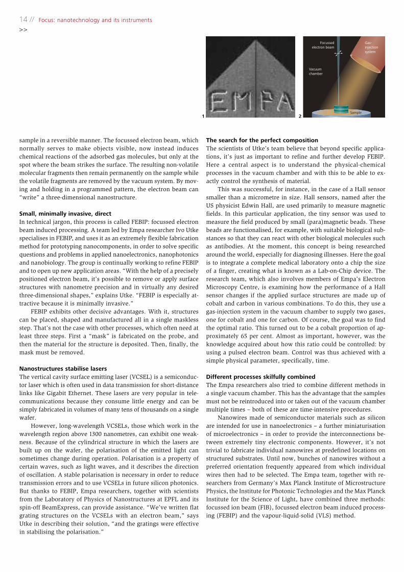
1,2The principle of the local deposition process which is induced with a focussed electron beam (in short, FEBIP): molecules from agas-injection system are deposited on the sample surface in a reversible manner. The focussed electron beam dissociates adsorbed gas molecules. The resulting non-volatile compounds remain permanently on the sample. The result is a nanostructure –for example the lettering for Empa – which has been written bythe movements of an electron beam.
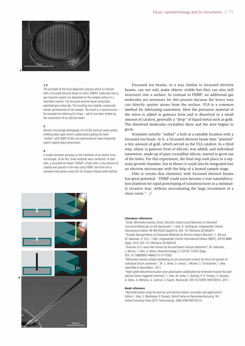
3Electron microscope photograph of a VCSEL (vertical cavity surfaceemitting laser) upon which a polarisation grating has been “written” with FEBIP. VCSELs are semiconductor lasers frequentlyused in optical data transmission.
4A single nanowire growing on the cantilever of an atomic force microscope. To do this, three methods were combined: to startwith, a focussed ion beam “drilled” a hole; then a tiny amount ofcatalyst was placed in the hole using FEBIP; and from this ananowire was grown using the VLS (vapour-liquid-solid) method.
3
4
10µm
500nm
16 // Knowledge and technology transfer
A “soft” shell and a “hard” core – for once, the reverse situation. Novel fibres enable the creation of artificial turf which meets the highest demands when playing football. Empa researchers,together with TISCA TIARA, a Swiss manufacturer of artificial turf, have developed a bi-componentfibre with two impressive qualities: thanks to a hard core it returns to an upright position againand again, and because of a soft sheath it avoids abrasions and grass burns.
TEXT: Nadja Kröner / PHOTOS: Empa, TISCA TIARA
Maybe it’s cold and wet outdoors, or perhapsit just snowed. It’s not exactly the best timeof year to play football, or is it? Thanks to arti -
ficial turf, for decades it’s been possible to play duringwinter, too. The artificial grass is robust and stands upto any weather. Even so, a few of us might remembersome painful injuries we got on artificial turf. The firstgeneration of that material was manufactured usingpolyamide fibres with excellent recovery propertiesand which always stood upright. But it’s exactly theseresistant fibres which frequently led to grass burns andabrasions whenever someone took a tumble.
That’s why second-generation fibres consisted ofpolyethylene whose properties were much gentler tothe skin. In practical use, however, these fibres alsoexhibited a serious defect: their resilience, or ability tostand upright after repeatedly being trampled upon,was very poor. Over time, the load on the fibres led toa downright flat pitch. That was not only visually un-attractive, the “bent over” blades of artificial grass alsochanged how well the turf could be played on. As a re-sult, an attempt was made to support the blades withsand or granulated material. Today, turf with a granu-lated infill is very common.
Modern artificial turfs such as SPORTISCA fromTISCA TIARA, a manufacturer of textile-based floorcoverings, meanwhile consist of three fibre layerswhich give them a relatively high degree of resiliency.Because the polyethylene fibres’ lack of shape stabilitycreated problems even early during production, thisfirm, which is based in the Appenzell region of Switzer-land, sought out Empa to help them find solutions.
“The requirements on artificial turf are quite varied,”notes Andreas Tischhauser, head of marketing at TISCATIARA. “For instance, footballers want an especiallysoft grass surface while pitch operators want one witha long service lifetime. And, of course, it must alsomeet ecological requirements.”
A development with many challengesIt was soon clear that a completely new fibre had to bedeveloped. It should exhibit high resilience as well asoptimal sliding friction behaviour. Two properties im-plies the need for two components, thought RudolfHufenus of Empa’s Advanced Fibers Laboratory tohimself. According to this idea, such a fibre shouldcontain a hard polyamide core surrounded by a low-friction sheath of polyethylene.
With the support of Christian Affolter, a modellingexpert in the Mechanical Systems Engineering Labora-tory, they simulated a variety of cross-sections whichwould best fulfil the desired requirements.
However, the development of the new fibre wasno easy task, as was discovered within the scope of aproject financed by the Swiss Innovation PromotionAgency CTI. “At half-time, we were clearly behind ourproject plan,” recalls Hufenus. The problem was thatthe modelling of all the various cross-sections wasclearly more complex than had been assumed and tookmore time than anticipated. The input parameters forthe models were the fibre’s cross-section geometryalong with the material properties of both polymers,which were determined through mechanical tests. Inaddition, the loading on the fibre, in other words how
Artificial turf with upstanding qualities
4
it should bend, was part of the model. All of this datafinally resulted in a simulation of the fibre’s stress-strain characteristics.
A further challenge arose because a new spinninghead had to be developed for Empa’s pilot spinningsystem in conjunction with the Institute for RapidProduct Development at ETH Zurich. The unusual as-pect about this spinning head was that the two poly-mers could be processed at different temperatures. Thebasis for the construction was the assumption that thetwo polymers being used had to be extruded at differ-ent temperatures. In the course of the project it wasdetermined that this isn’t necessary.
The industrial production of the fibres also provedchallenging because they need spinning systems de-signed specifically for fibres going into artificial turf,which are generally not two-component systems. “Af-ter we worked very hard to persuade him to do so, thefibre manufacturer we brought into this project told ushe was prepared to modify his spinning systems as re-quired,” explains Hufenus. The time from planning toconstruction was a full year.
With trial and error to the optimum fibreEven at the conclusion of the project, when the com-pleted fibre was on hand, yet another difficulty arose– the fibres did not pass the Lisport test, which checksfor long-term mechanical wear. The sheath of the two-component fibres separated from the core with timewhen placed under load. TISCA TIARA then furtheroptimised the fibre after consultation with and sup-port from Hufenus. “We proceeded according to the
trial-and-error method in which we simply tried outvarious options until we found the best possible cross-section,” says Tischhauser.
Finally everything was complete; with much pa-tience they had succeeded in creating an optimal cross-section: instead of a thick core, the fibre consists offive thin ones. The fibre’s resiliency qualities are guar-anteed for years, as a new Lisport test was able toprove. “We’re the first ones who have followed sucha project through from the development of the fibre tothe laying of the artificial turf,” boasts Hufenus proud-ly. Tischhauser is also very pleased, saying, “We couldhardly believe that all at once everything worked out.”
The turf, which visually comes very close to thenatural grass which it is intended to imitate, has alreadybeen laid on two football pitches, one in Ecublens nearLausanne and the other in Bürglen in the canton ofThurgau – and to the complete satisfaction of the foot-ballers. “With this, we fulfilled the essential require-ments of our industrial partner TISCA TIARA for a newfibre used in artificial turf,” adds Hufenus.
A FIFA certification isn’t anything to worry about,however, because at this time the standards are in facttrailing technological developments and effectivelygive a chance only to artificial turf with a granulatedinfill. Nevertheless, because of its clearly superior prop-erties, the new artificial turf will surely be a marketsuccess because most football pitches don’t requireFIFA certification. In addition, it’s more important forthe teams that they can play, and more importantlytrain, in grey, wet weather and in snow than it is to beon certified turf. //
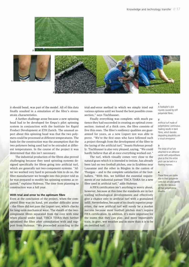
1A footballer’s skin injuries caused by stiffpolyamide fibres.
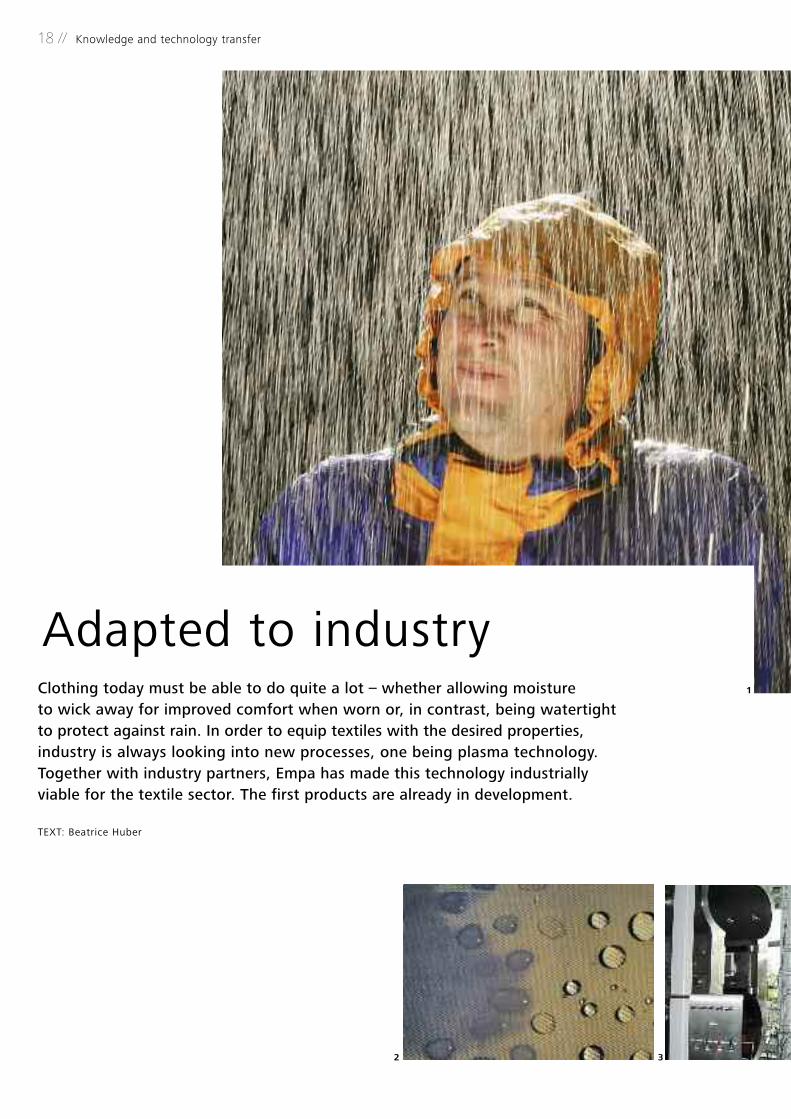
2Artificial turf made ofpolyethylene: continuousloading results in bentfibres, which besides degrading playability area visual annoyance.
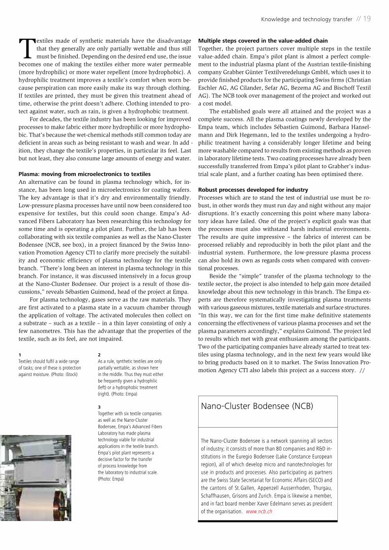
3The strips of turf are attached to an adhesivecarrier with polyurethaneglue so that the entirepitch can be laid in afloating manner.
4These fibres are stabledue to their polyamidecores but are also gentleon the skin because of their polyethylenesheaths.
1
2
Knowledge and technology transfer // 17
3
18 // Knowledge and technology transfer
1
2 3
Clothing today must be able to do quite a lot – whether allowing moisture to wick away for improved comfort when worn or, in contrast, being watertight to protect against rain. In order to equip textiles with the desired properties,industry is always looking into new processes, one being plasma technology.Together with industry partners, Empa has made this technology industrially viable for the textile sector. The first products are already in development.
TEXT: Beatrice Huber
Adapted to industry
Textiles made of synthetic materials have the disadvantagethat they generally are only partially wettable and thus stillmust be finished. Depending on the desired end use, the issue
becomes one of making the textiles either more water permeable(more hydrophilic) or more water repellent (more hydrophobic). Ahydrophilic treatment improves a textile’s comfort when worn be-cause perspiration can more easily make its way through clothing.If textiles are printed, they must be given this treatment ahead oftime, otherwise the print doesn’t adhere. Clothing intended to pro-tect against water, such as rain, is given a hydrophobic treatment.
For decades, the textile industry has been looking for improvedprocesses to make fabric either more hydrophilic or more hydropho-bic. That’s because the wet-chemical methods still common today aredeficient in areas such as being resistant to wash and wear. In add -ition, they change the textile’s properties, in particular its feel. Lastbut not least, they also consume large amounts of energy and water.
Plasma: moving from microelectronics to textilesAn alternative can be found in plasma technology which, for in-stance, has been long used in microelectronics for coating wafers.The key advantage is that it’s dry and environmentally friendly.Low-pressure plasma processes have until now been considered tooexpensive for textiles, but this could soon change. Empa’s Ad-vanced Fibers Laboratory has been researching this technology forsome time and is operating a pilot plant. Further, the lab has beencollaborating with six textile companies as well as the Nano-ClusterBodensee (NCB, see box), in a project financed by the Swiss Inno-vation Promotion Agency CTI to clarify more precisely the suitabil-ity and economic efficiency of plasma technology for the textilebranch. “There’s long been an interest in plasma technology in thisbranch. For instance, it was discussed intensively in a focus groupat the Nano-Cluster Bodensee. Our project is a result of those dis-cussions,” reveals Sébastien Guimond, head of the project at Empa.
For plasma technology, gases serve as the raw materials. Theyare first activated to a plasma state in a vacuum chamber throughthe application of voltage. The activated molecules then collect ona substrate – such as a textile – in a thin layer consisting of only afew nanometres. This has the advantage that the properties of thetextile, such as its feel, are not impaired.
Multiple steps covered in the value-added chainTogether, the project partners cover multiple steps in the textilevalue-added chain. Empa’s pilot plant is almost a perfect comple-ment to the industrial plasma plant of the Austrian textile-finishingcompany Grabher Günter Textilveredelungs GmbH, which uses it toprovide finished products for the participating Swiss firms (ChristianEschler AG, AG Cilander, Sefar AG, Bezema AG and Bischoff TextilAG). The NCB took over management of the project and worked outa cost model.
The established goals were all attained and the project was acomplete success. All the plasma coatings newly developed by theEmpa team, which includes Sébastien Guimond, Barbara Hansel-mann and Dirk Hegemann, led to the textiles undergoing a hydro -philic treatment having a considerably longer lifetime and beingmore washable compared to results from existing methods as provenin laboratory lifetime tests. Two coating processes have already beensuccessfully transferred from Empa’s pilot plant to Grabher’s indus-trial scale plant, and a further coating has been optimised there.
Robust processes developed for industryProcesses which are to stand the test of industrial use must be ro-bust, in other words they must run day and night without any majordisruptions. It’s exactly concerning this point where many labora -tory ideas have failed. One of the project’s explicit goals was thatthe processes must also withstand harsh industrial environments.The results are quite impressive – the fabrics of interest can beprocessed reliably and reproducibly in both the pilot plant and theindustrial system. Furthermore, the low-pressure plasma processcan also hold its own as regards costs when compared with conven-tional processes.
Beside the “simple” transfer of the plasma technology to thetextile sector, the project is also intended to help gain more detailedknowledge about this new technology in this branch. The Empa ex-perts are therefore systematically investigating plasma treatmentswith various gaseous mixtures, textile materials and surface structures.“In this way, we can for the first time make definitive statementsconcerning the effectiveness of various plasma processes and set theplasma parameters accordingly,” explains Guimond. The project ledto results which met with great enthusiasm among the participants.Two of the participating companies have already started to treat tex-tiles using plasma technology, and in the next few years would liketo bring products based on it to market. The Swiss Innovation Pro-motion Agency CTI also labels this project as a success story. //
Knowledge and technology transfer // 19
Nano-Cluster Bodensee (NCB)
The Nano-Cluster Bodensee is a network spanning all sectorsof industry; it consists of more than 80 companies and R&D in-stitutions in the Euregio Bodensee (Lake Constance Europeanregion), all of which develop micro and nanotechnologies foruse in products and processes. Also participating as partnersare the Swiss State Secretariat for Economic Affairs (SECO) andthe cantons of St.Gallen, Appenzell Ausserrhoden, Thurgau,Schaffhausen, Grisons and Zurich. Empa is likewise a member,and in fact board member Xaver Edelmann serves as presidentof the organisation. www.ncb.ch
1Textiles should fulfil a wide range of tasks; one of these is protectionagainst moisture. (Photo: iStock)
2As a rule, synthetic textiles are onlypartially wettable, as shown here in the middle. Thus they must eitherbe frequently given a hydrophilic(left) or a hydrophobic treatment(right). (Photo: Empa)
3Together with six textile companiesas well as the Nano-Cluster Bodensee, Empa’s Advanced Fibers Laboratory has made plasma technology viable for industrial applications in the textile branch.Empa’s pilot plant represents a decisive factor for the transfer of process knowledge from the laboratory to industrial scale. (Photo: Empa)
Switch cabinetsControl board
Assembly
DesignerMAIN UNIT UNIT UNIT UNIT
ELECTRONICS
Up to 30 suppliers
Diodes LEDs
Coils
Resistance
etc.
ICs
Clamps
Condenser
Control unit Generator
26 // Im Dialog
Small but by no means unimportant: defective electronic components can lead to malfunctions, not only in computer systems but also in entiretransportation systems or power plants, and as a result incur enormous expense. Troubleshooting is generally very difficult, especially if the components don’t exhibit any manufacturing defects. Experts at Empa are playing the role of detective for industry and have taken causal research to the highest level.
TEXT: Martina Peter
In a complex electronic system, thou-sands upon thousands of componentsand modules must work together smooth-
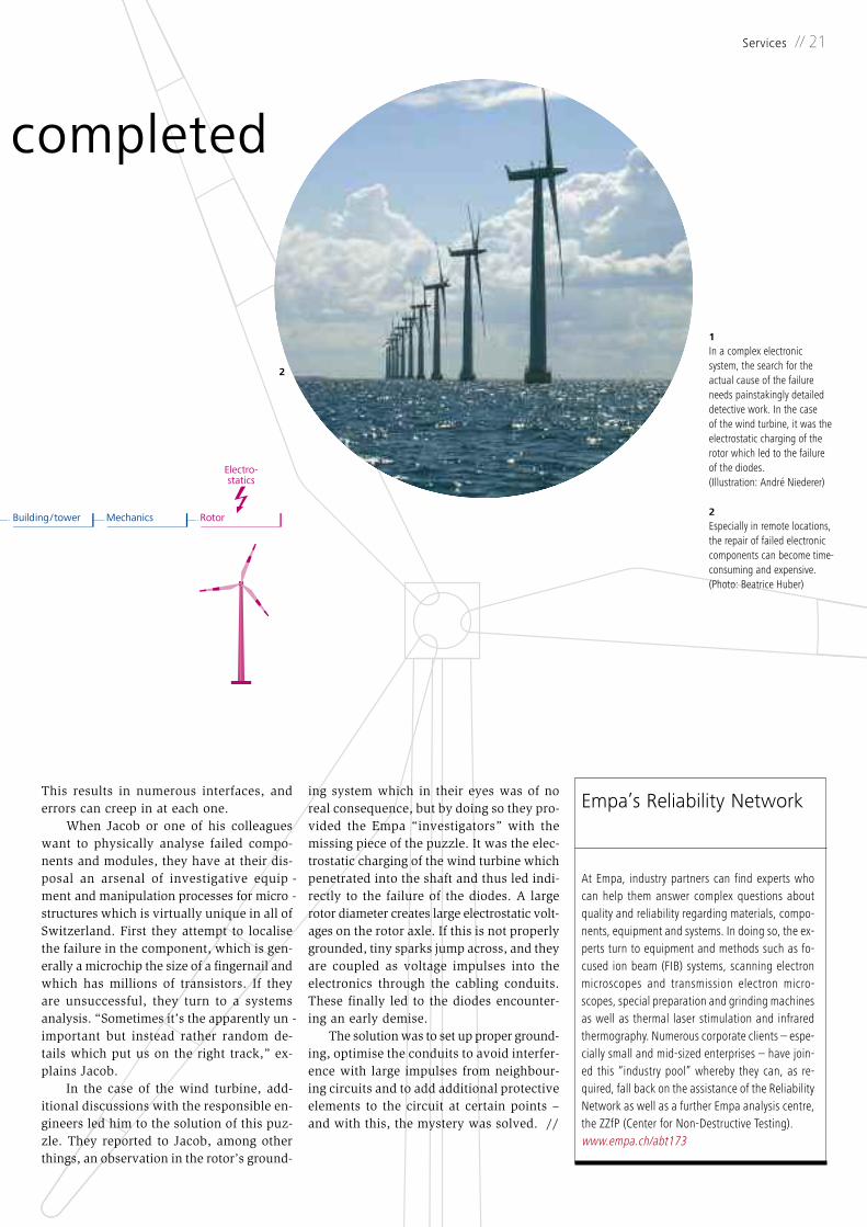
ly. If there’s a system outage, virtually aninfinite number of errors could be respon-sible; for some individual microchips around400 failure classes have already been de-fined. It’s almost like trying to find theproverbial needle in a haystack when – asrecently happened in a wind turbine – forno apparent reason, perfectly good diodesstart failing on a regular basis.
That’s a problem right up the alley ofEmpa researcher Peter Jacob, who joinswith other experts in microelectronics, andtogether they use their skills as sleuths toinvestigate such failures as well as to un-cover weaknesses in components, circuitsand their applications. In the process theybring some surprising results to the light ofday. The team from the Electronics/Metrol-ogy Laboratory operates as do specialised
physicians in a group practice. The “patients”of Empa’s Reliability Network are compo-nents and modules from power electronics,micro electronics and optoelectronics. “Wereceive enquiries from industrial customerswho frequently expect the worst,” accord-ing to Jacob. That’s because many fear ex-tremely high costs as a consequence of asystem failure.
As would a doctor, the Empa expertsfirst conduct a diagnosis meeting. They ex-amine factors such as how the interconnec-tions in the application are laid out, whodelivered the modules or how long a com-ponent has been in use. In the case of thewind turbine, however, neither did thecomponents exhibit manufacturing defectsnor did the schematics reveal any defects.Nonetheless, small diodes were failing inthe same location in a module with inte-grated rectifiers. Redundant systems – atype of replacement system which steps in
if there is ever an operating malfunction –prevent higher level components, in thiscase the generator control system, from being affected. Even so, the continuous re-pair work proved extremely time-consum-ing and expensive in the remotely locatedwind turbines. It was thus the proper timeto commission the Empa experts to searchfor the actual cause of the failure.
Painstakingly detailed detective workConstructing a technical system such as awind turbine is almost as complicated asthe control systems it contains. One sup -plier erects the tower and turbine blades,while another develops the required con-trol systems, which in turn contain count-less electronic components from furthermanufacturers that are finally assembledinto the overall control system by a furtherpartner in the manufacturing chain. Having30 or more suppliers involved is not unusual.
Debugging – successfully
20 // Services
1
Building/tower Mechanics Rotor
Electro-statics
Im Dialog // 27
This results in numerous interfaces, and errors can creep in at each one.
When Jacob or one of his colleagueswant to physically analyse failed compo-nents and modules, they have at their dis-posal an arsenal of investigative equip -ment and manipulation processes for micro -structures which is virtually unique in all ofSwitzerland. First they attempt to localisethe failure in the component, which is gen-erally a microchip the size of a fingernail andwhich has millions of transistors. If theyare unsuccessful, they turn to a systemsanalysis. “Sometimes it’s the apparently un -important but instead rather random de-tails which put us on the right track,” ex-plains Jacob.
In the case of the wind turbine, add -itional discussions with the responsible en-gineers led him to the solution of this puz-zle. They reported to Jacob, among otherthings, an observation in the rotor’s ground-
ing system which in their eyes was of noreal consequence, but by doing so they pro-vided the Empa “investigators” with themissing piece of the puzzle. It was the elec-trostatic charging of the wind turbine whichpenetrated into the shaft and thus led indi-rectly to the failure of the diodes. A largerotor diameter creates large electrostatic volt-ages on the rotor axle. If this is not properlygrounded, tiny sparks jump across, and theyare coupled as voltage impulses into theelectronics through the cabling conduits.These finally led to the diodes encounter-ing an early demise.
The solution was to set up proper ground-ing, optimise the conduits to avoid interfer-ence with large impulses from neighbour-ing circuits and to add additional protectiveelements to the circuit at certain points –and with this, the mystery was solved. //
completed
Services // 21
Empa’s Reliability Network
At Empa, industry partners can find experts whocan help them answer complex questions aboutquality and reliability regarding materials, compo-nents, equipment and systems. In doing so, the ex-perts turn to equipment and methods such as fo-cused ion beam (FIB) systems, scanning electronmicroscopes and transmission electron micro-scopes, special preparation and grinding machinesas well as thermal laser stimulation and infraredthermography. Numerous corporate clients – espe-cially small and mid-sized enterprises – have join -ed this “industry pool” whereby they can, as re-quired, fall back on the assistance of the ReliabilityNetwork as well as a further Empa analysis centre,the ZZfP (Center for Non-Destructive Testing).www.empa.ch/abt173
2
1In a complex electronic system, the search for the actual cause of the failureneeds painstakingly detailed detective work. In the case of the wind turbine, it was theelectrostatic charging of therotor which led to the failureof the diodes. (Illustration: André Niederer)
2Especially in remote locations,the repair of failed electronic components can become time-consuming and expensive. (Photo: Beatrice Huber)
22 // Science dialogue
Visit by the cantonal Governmentof St.Gallen
On 19 October, Empa in St.Gallen wel-comed some distinguished guests: the en-tire cantonal Government paid a visit andthe scientists at Empa gave a comprehen-sive view into their research activities. Themembers of the government were clearlyimpressed by what they saw.
EmpaNews in e-paper format
Just recently, in addition to the printededition of EmpaNews, it has become pos-sible to receive the magazine in e-paperformat and thus paper-free.Simply go to the EmpaNews home
page (www.empanews.ch) and click onthe related icon in the right-hand column.Then you can instantly comb throughpast issues starting with #21, in otherwords, since the redesign of the researchmagazine in 2008. The web page also of-fers access to additional Empa publica-tions as PDFs which you can flip throughon your computer. Of course, it’s also pos-sible to store or print individual pagesand articles.
Swiss Innovation Forum 2010
At the 5th Swiss Innovation Forum on 4 November in Basel, Empa presented itspilot’s suit which was custom-made for Solar Impulse – an aircraft designed topursue the goal of circumnavigating the globe using only solar energy. So thatthe pilots neither perspire nor freeze during the flight stages, which will last aslong as five days and nights, special clothing systems are needed. When devel-oping the pilot’s suit, Empa reverted to an old, proven material; down, whichhas an extremely high level of thermal insulation and transports moisture quitewell. During the first night flight of Solar Impulse at the beginning of July 2010,the suit passed its initial “acid test”.
Prize awarded to OptotuneThe Swiss Technology Award, which has been awarded since 2007 within thescope of the Swiss Innovation Forum, this year went to Optotune in the category“Start-up”. Founded in 2008 as a spin-off of ETH Zurich, Optotune has its officesin Empa’s glaTec technology centre in Dübendorf. Together with Empa re-searchers, the entrepreneurial company develops, among other things, opticalsystems which progressively vary the refractive power of a lens with the helpof “artificial muscles” and in a way similar to the human eye. Meanwhile, thenumber of employees at Optotune has grown to 20.
Science dialogue // 23
Education week for young researchers
At the start of November, eleven young researchers – including three fromEmpa – spent a week travelling throughout Switzerland. They obtained insightsinto current research and development efforts as well as production require-ments in the (bio)materials sector from a variety of companies as well as clin-ical and academic institutions. This “travelling lab workshop” is part of theeducational activities of CCMX, the Competence Centre for Materials Scienceand Technology of the ETH Domain, in which Empa participates. Educationplays a central role in the Competence Centre. During the workshop, partici-pants were allowed to not only watch but were also required to take an activerole in case studies and collaborate in practical problem-solving as well as in-troduce and discuss their own research projects. The workshop was organisedby Katharina Maniura, co-head of Empa’s Materials-Biology Interactions Lab-oratory and head of the CCMX MatLife Program; she accompanied the groupthroughout the week.
Left: The Tesla Roadster, easily the best-known electric sports car, accelerates in only four seconds fromzero to 100 km/hr – without making any noise. Right: Driving with natural gas, and especially biogas,significantly reduces CO2 emissions.
Let the wind flow…
Last year Empa constructed a new windtunnel which the Laboratory of BuildingScience and Technology will use to studythe behaviour of wind currents in cities.On 11 March, the official opening willtake place with a symposium entitled En-ergy and Wind Research for Future Citiesand Societies; it is targeted at architects,space planners, urban planners and scien-tists as well as interested members of thegeneral public.
Take the train to Empa
Now it’s possible – since the middle of De-cember, the Glattalbahn metropolitan rail-way connects Empa in Dübendorf directlywith the Zurich Airport and the Stettbachtrain station. At the opening festivities forthe new Line 12, Empa displayed newdrive technologies using test vehicles andprototypes which function with hydrogen,electricity or natural gas/biogas. In add -ition, the very numerous visitors were ableto experience at first-hand research pro -jects dealing with noise and fire protectionin transportation. Further, on the Empagrounds they had the opportunity to in-spect the new wind tunnel (see the item“Let the wind flow…”) along with “Self”,a living module for residential and work-ing purposes, which is self-sufficient in en-ergy and water consumption.
Technology Days 2010
Mobility is an important pillar which supports the Swiss economy – but alsoa problem child on our way to a sustainable development. This raises the ques-tion as to how individual mobility can be guaranteed without putting an unduestrain on people and the environment over the long term. To address this topic,the Technology Days 2010, sponsored by Swiss Engineering STV, SATW (SwissAcademy of Engineering Sciences) and Empa, delivered answers under the slo-gan, “Sustainable Mobility”. An exhibition during the central event on 27 Octo-ber at Empa in Dübendorf illustrated how multifaceted mobility already is today.Interested visitors were able to take a test drive in gas and electric vehicles.
Events11 March 2011Let the wind flowSymposium to mark the opening of the wind tunnel at Empa Empa, Dübendorf
16 March 2011Earthquake-resistant multi-storey wooden buildingsFor construction engineers and wood-frame specialistsEmpa, Dübendorf
22 March 2011Nanofabrication and nanoanalysis with focusedelectron and ion beams (FEB, FIB)Empa/FSRM courseEmpa, Dübendorf
25 March 2011 Challenges and opportunities of diesel particle filter technologiesFor representatives in the particle-filter industry, govern-ment officials and members of the VERT AssociationEmpa, Dübendorf
5 April 2011Aluminium alloysEmpa/FSRM courseEmpa, Dübendorf
16 May 2011 Blended and alternative cementsFor R&D professionals working with cement, mortar and concreteEmpa, Dübendorf
18 and 19 May 2011 Swiss NanoConvention 2011For interested parties from science and industryTRAFO Culture and Conference Centre, Baden
For details and further events: www.empa-akademie.ch
Your way to access Empa’s know-how:
We found the
cooperation among
the various branches
of science and the
latest achievements
very impressive,
as well as the interfaces
between science and
applications.
Willi HaagPresident of the cantonal Government, St.Gallen
“
Opinion
Willi Haag
[email protected] +41 44 823 44 44www.empa.ch/portal”