Embed Size (px)
Citation preview
© 2015 Freescale Semiconductor, Inc. All rights reserved.
Emulating I2C Bus Master by using FlexIO
1. Introduction
This application note lists the steps to use the FlexIO
module for emulating the I2C bus master.
FlexIO is a new on-chip peripheral available on some of
the Kinetis microcontrollers. It is highly configurable,
capable of emulating a wide range of communication
protocols, such as UART, I2C, SPI, I2S, and so on. You
can use FlexIO for generating PWM/Waveform and
building your own peripherals directly.
2. Overview of the FlexIO module
The hardware resources in FlexIO module are:
• Shifter
• Timer
• Pin
The amount of these resources for a given
microcontroller is read from the FLEXIO_PARAM
register. For example, there are four shifters, four
timers, and eight pins in KL27Z64.
Figure 1 shows a high-level overview of the FlexIO
module.
Freescale Semiconductor, Inc. Document Number: AN5133
Application Notes Rev. 0 , 06/2015
Contents
1. Introduction ........................................................................ 1 2. Overview of the FlexIO module......................................... 1 3. Emulating I2C bus Master by using FlexIO ....................... 3
3.1. General description ................................................. 3 3.2. Configurations of the shifters and timers ................ 4 3.3. Software implementation overview ........................ 7 3.4. Running the demos ................................................. 8
4. Conclusion ....................................................................... 11 5. Additional information ..................................................... 11 6. References ........................................................................ 11

Overview of the FlexIO module
Emulating I2C Bus Master by using FlexIO, Rev. 0, 06/2015
2 Freescale Semiconductor, Inc.
Figure 1. FlexIO block diagram
The key features are:
• 32-bit shifters with transmit, receive, and data match modes.
• Double buffered shifter operation.
• 16-bit timers with high flexibility support for a variety of internal or external triggers, and Reset/
Enable/ Disable/ Decrement conditions.
• Automatic start/stop bit generation/check.
• Interrupt, DMA or polling mode operation.
• Shifters, timers, pins, and triggers can be flexibly combined to operate.
Transmit and receive are two basic modes of the shifters. If one shifter is configured as transmit mode, it
loads data from its buffer register and shifts data out to its assigned pin bit by bit. If one shifter is
configured as receive mode, it shifts data in from its assigned pin and stores data into its buffer register.
The load, store, and shift operations are all controlled by the shifter’s assigned timer.
You can also configure the timers as different operation modes according to the requirement, including
dual 8-bit counters baud/bit mode, dual 8-bit counters PWM mode, and single 16-bit counter mode.

Emulating I2C bus Master by using FlexIO
Emulating I2C Bus Master by using FlexIO, Rev. 0, 06/2015
Freescale Semiconductor, Inc. 3
3. Emulating I2C bus Master by using FlexIO
This section describes how to emulate I2C bus master with FlexIO. For this application, the Freescale
Freedom development board FRDM-KL27Z shown in Figure 2 has been used.
Figure 2. Freescale Freedom development board FRDM-KL27Z
In the application, Flexio emulates an I2C interface to communicate with the three-axis accelerometer
MMA8451Q, in which a general I2C interface is integrated. The data read from MMA8451Q is sent to
PC terminal through a UART port.
The following diagram shows the hardware platform and data flows. For more information on Open-
SDA in the diagram, see the relevant materials of the Freescale Freedom development board.)
Figure 3. Hardware Platform and Data Flows of this Application
3.1. General description
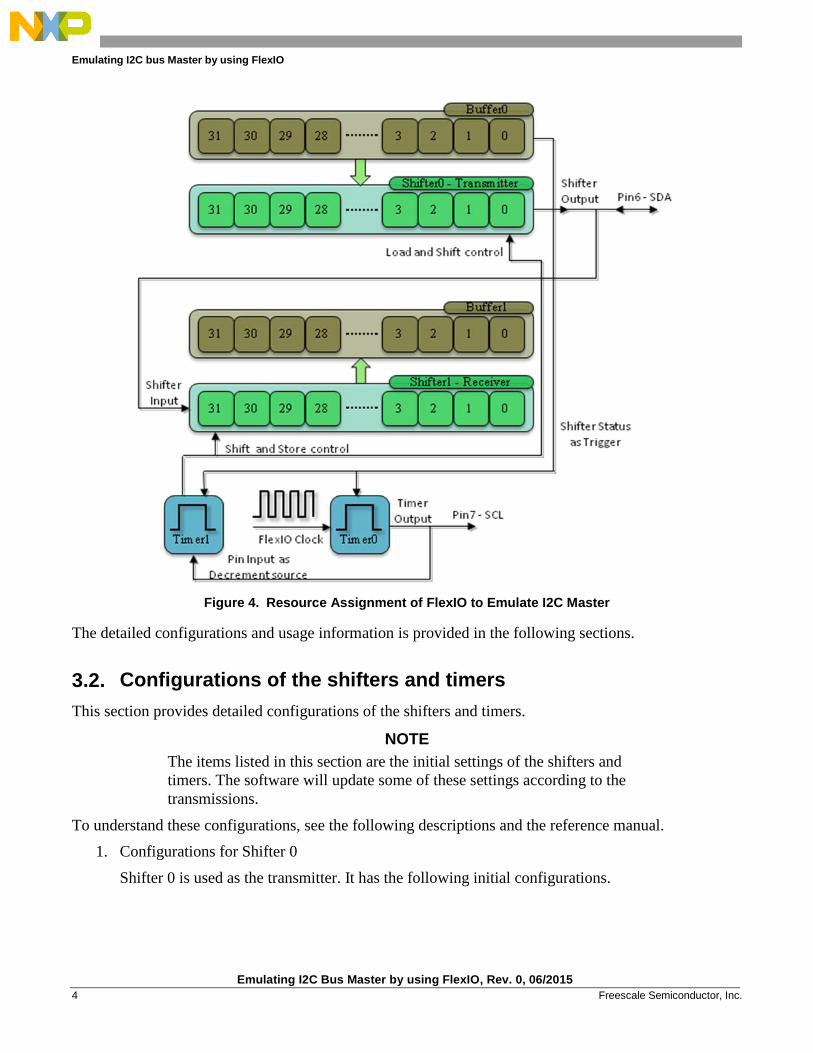
I2C bus master is emulated using:
• Two shifters — Respectively used as a transmitter and a receiver.
• Two timers —One is used for the SCL output generation, and the other is used for the
load/store/shift control of the two shifters.
• Two pins — Respectively used as SDA and SCL.
Figure 4 shows the resource assignment.
X
Y
KL27Z64 MMA8451Q
Emulating I2C bus Master by using FlexIO
Emulating I2C Bus Master by using FlexIO, Rev. 0, 06/2015
4 Freescale Semiconductor, Inc.
Figure 4. Resource Assignment of FlexIO to Emulate I2C Master
The detailed configurations and usage information is provided in the following sections.
3.2. Configurations of the shifters and timers
This section provides detailed configurations of the shifters and timers.
NOTE
The items listed in this section are the initial settings of the shifters and
timers. The software will update some of these settings according to the
transmissions.
To understand these configurations, see the following descriptions and the reference manual.
1. Configurations for Shifter 0
Shifter 0 is used as the transmitter. It has the following initial configurations.

Emulating I2C bus Master by using FlexIO
Emulating I2C Bus Master by using FlexIO, Rev. 0, 06/2015
Freescale Semiconductor, Inc. 5
Table 1. Initial configuration of Shifter 0
Items Configurations
Shifter mode Transmit
Timer selection Timer 1
Timer polarity On posedge of shift clock
Pin selection Pin 6
Pin configuration Ppen drain or bidirectional output enable
Pin polarity Active low
Input source From pin
Start bit Value 0
Stop bit Value 1
Buffer used Bit Byte Swapped Register
2. Configurations for Shifter 1
Shifter 1 is used as the receiver. It has the following initial configurations.
Table 2. Initial configuration of Shifter 1
Items Configurations
Shifter mode Receive
Timer selection Timer 1
Timer polarity On negedge of shift clock
Pin selection Pin6
Pin configuration Output disabled
Pin polarity Active high
Input source fFrom pin
Start bit Disabled
Stop bit Value 0
Buffer used Bit Byte Swapped Register
3. Configurations for Timer 0
Timer 0 is used to generate SCL output and to trigger timer 1. It has the following initial
configurations.
Table 3. Initial configuration of Timer 0
Items Configurations
Timer mode Dual 8-bit baud/bit mode
Trigger selection Shifter 0 status flag
Trigger polarity Active low
Trigger source Internal
Pin selection Pin 7
Pin configuration Open drain or bidirectional output enable
Pin polarity Active high
Timer initial output Output logic 0 when enabled, not affect by reset
Timer decrement source Decrement on FlexIO clock, Shift on timer output
Timer enable condition On trigger high
Timer disable condition On timer compare

Emulating I2C bus Master by using FlexIO
Emulating I2C Bus Master by using FlexIO, Rev. 0, 06/2015
6 Freescale Semiconductor, Inc.
Timer reset condition On timer pin equals to timer output
Start bit Enabled
Stop bit Enabled on timer disable
Timer compare value (((n*9+1)*2-1)<<8) | baudrate_divider1
[1] n - the number of bytes in the transmission
baudrate_divider - a value used for dividing baud rate from FlexIO clock source
4. Configurations for Timer 1
Timer 1 is used to control the Shifter 0 and Shifter 1. It has the following initial configurations.
Table 4. Initial configuration of Timer 1
Items Configurations
Timer mode Single 16-bit counter mode
Trigger selection Shifter0 status flag
Trigger polarity Active low
Trigger source Internal
Pin selection Pin 7
Pin configuration Output disabled
Pin polarity Active low
Timer initial output Output logic 1 when enabled, not affect by reset
Timer decrement source Decrement on pin input, shift clock equal to pin input
Timer enable condition On timer 0 enable
Timer disable condition On timer 0 disable
Timer reset condition Never reset
Start bit Enabled
Stop bit Enabled on timer compare
Timer compare value 0x0F
The following tips are the key points of using FlexIO to emulate I2C bus master.
• Dealing with the transmitter and receiver: From the above configurations, you can see that
there are two shifters, sharing one timer (Timer 1) and SDA pin (Pin 6), respectively used as the
transmitter and receiver. So, both of the shifters are serviced for each byte in the transmissions.
The receiver is read after each byte transmission to clear the receive buffer and status flag. The
transmitter must transmit 0xFF to tristate the output when receiving.
• Timer trigger settings: The triggers of the timers are set as the transmitter’s status flag. Filling a
byte into the transmitter’s buffer negates the status flag enables the timer 0 to start the decrement
count. The decrement source of timer 1 is set as the SCL pin input. Each SCL edge makes timer
1 to decrease by 1. Two SCL edges make timer 1to go through one period, which results in the
data in the shifters to shift by one bit.
• TIMCMP (Timer Compare Register) settings: TIMCMP of a timer stores the timer’s module
value. The high 8 bits of TIMCMP 0 need to be set to a value that equals to the amount of SCL
edges (both edges) in a transmission. The number of the data bytes, ACK/NACK bit, and stop-
condition bit should be taken into consideration when calculating the value. The low 8 bits of
TIMCMP 0 are used to configure the baud rate. The value set to TIMCMP 1 is calculated based
on the number bits in a single frame.
Emulating I2C bus Master by using FlexIO
Emulating I2C Bus Master by using FlexIO, Rev. 0, 06/2015
Freescale Semiconductor, Inc. 7
• Operations for double-buffered shifters: The shifters are designed as double-buffered
structure. To avoid underflow when transmitting or receiving multiple bytes in high baud rate,
the transmit shifter and its buffer should be filled data by software in advance. The process can
be divided into the following steps: (1) Filling the first byte into the transmit buffer; (2) Waiting
for the first byte to be loaded into the transmit shifter by polling the status flag. Filling the
second byte into the transmit buffer; (3) Waiting for the first byte is shifted out and the second
byte is loaded into the transmit shifter. The first received byte is shifted into the receive shifter
during this period. Waiting for the first received byte to be stored into the receive buffer.
Reading the receive buffer. Filling the third byte into the transmit buffer. From the third step to
the last, polling /interrupt/DMA mode can be used. In respect of the time delay, DMA is less
than interrupt, and interrupt is less than polling.
• ACK/ NACK bit generation and check: An ACK or NACK bit is needed after each
transmission in I2C bus protocol. The SSTOP bit of the transmitter can be used to generate
ACK/NACK. Set SSTOP bit to 0 to generate ACK, and set it to 1 to generate NACK. The
SSTOP bit of the receiver can be used to check ACK/NACK. To shift the ACK/NACK bit
out/in, timer 0 needs to output two additional edges. When timer 1 has decreased to 0, the
following SCL configured edge will shift the ACK/NACK bit out/in.
• Repeated START and STOP signal generation: As a (repeated) START signal is a falling
edge and STOP signal is a rising edge of SDA during SCL in high level. Therefore, SDA needs
to be set to high in advance (during SCL in low level) to generate repeated START signal, and
set to low to generate STOP signal. These can be implemented by loading one additional byte
into transmitter on the last falling edge of SCL in each byte transmission. However, only the
highest bit will be shifted out. This is also controlled by the timers. Therefore, 0xFF is loaded if
generating a repeated START signal, and 0x00 is loaded if generating a STOP signal. The
(repeated) START and STOP signal’s level are respectively determined by the SSTART and
SSTOP in the transmitter Shifter Configuration Register. Before the first data bit shifts out, the
configured start bit is loaded into the transmit shifter and is then shifted out. When timer 0
decrement counts to 0, the configured stop bit will be load into transmit shifter and then shifted
out. Another point, the shifter will immediately load the stop bit when the shifter is initially
configured for transmit mode if a stop bit is enabled.
3.3. Software implementation overview
This section describes the software implementation. Several driver functions have been implemented in
this application, which are based on the HAL (Hardware Abstraction Layer) of the Freescale KSDK
(Kinetis Software Development Kit).
A software package is provided along with this application note. The package contains a pruned KSDK
based on V1.1, which this application needed.
There are two IAR projects in the software package. One works in polling mode, another in interrupt
mode. This section mainly describes several major driver functions, taking the polling demo for
example, as there is no much difference between the two modes in the respect of dealing with the
transmitter and receiver.
1. Initialize Function
The Initialize Function is used to configure the shifters and timers in the application’s

Emulating I2C bus Master by using FlexIO
Emulating I2C Bus Master by using FlexIO, Rev. 0, 06/2015
8 Freescale Semiconductor, Inc.
initialization phase. The prototype is:
void FlexIO_I2C_Init(void)
2. SCL Timer Compare Register Configuration Function
This function is used to set the SCL TIMCMP (TIMCMP 0) value according to the number of
bytes in a transmission. The prototype is:
void FlexIO_I2C_SetByteCounts(uint8_t n)
where,
— n — the number of bytes in the transmission
3. Transmit Function
This function is used to transmit one or more bytes to a given address of the slave device. The
prototype is:
void FlexIO_I2C_Transmit(uint8_t SlaveAddr, uint8_t RegisterAddr, uint8_t *TXDataBuffer,
uint8_t TransferSize)
where,
— SlaveAddr — Slave address on I2C bus;
— RegisterAddr — Register address to write of the slave device;
— TXDataBuffer — RAM buffer used to store the transmitted bytes;
— TransferSize — The number of the bytes to transmit.
4. Receive Function
This function is used to receive one or more bytes from a given address of the slave device. The
prototype is:
void FlexIO_I2C_Receive(uint8_t SlaveAddr, uint8_t RegisterAddr, uint8_t *RXDataBuffer,
uint8_t TransferSize)
— SlaveAddr — Slave address on I2C bus;
— RegisterAddr — Register address to read of the slave device;
— RXDataBuffer — RAM buffer used to store the received bytes;
— TransferSize — The number of the bytes to receive.
3.4. Running the demos
The user can download a program image to the microcontroller through Open-SDA. The PC host obtains
a serial port after a USB cable is connected between the PC host and the Open-SDA USB socket on
FRDM-KL27Z. Open a serial terminal, with these settings: 115200 baud rate, 8 data bits, no parity, one
stop bit, no flow control.
The project and workspace files of the polling demo are located in:
/demos/ flexio_i2c_polling /iar /frdmkl27z/
The source file is located in:
Emulating I2C bus Master by using FlexIO
Emulating I2C Bus Master by using FlexIO, Rev. 0, 06/2015
Freescale Semiconductor, Inc. 9
/demos/ flexio_i2c_polling /src/
The project and workspace files of the interrupt demo are located in /demos/ flexio_i2c_interrupt /iar
/frdmkl27z/. The source file is located in /demos/ flexio_i2c_interrupt /src/.
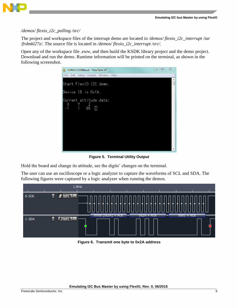
Open any of the workspace file .eww, and then build the KSDK library project and the demo project.
Download and run the demo. Runtime information will be printed on the terminal, as shown in the
following screenshot.
Figure 5. Terminal Utility Output
Hold the board and change its attitude, see the digits’ changes on the terminal.
The user can use an oscilloscope or a logic analyzer to capture the waveforms of SCL and SDA. The
following figures were captured by a logic analyzer when running the demos.
Figure 6. Transmit one byte to 0x2A address

Emulating I2C bus Master by using FlexIO
Emulating I2C Bus Master by using FlexIO, Rev. 0, 06/2015
10 Freescale Semiconductor, Inc.
Figure 7. Transmit three bytes to 0x23 address
Figure 8. Receive one byte from 0x0D address
Figure 9. Receive six bytes from 0x01 address
The I2C slave addresses of MMA8451Q are 0x3A for writing and 0x3B for reading. In MMA8451Q,
0x2A is the Control 1 Register’s address. 0x23 ~ 0x25 are the pulse threshold Registers’ addresses.
0x0D is the Device ID Register’s address. 0x01 ~ 0x06 are the Data Registers’ addresses. For detailed
information, please refer to MMA8451Q’s datasheet.
The test results showed that both the polling and interrupt demos are able to communicate with
MMA8451Q in a baud rate from 100 KHz to 400 KHz (MMA8451Q supports as high as 400 KHz).
In general, the baud rate that using FlexIO to emulate I2C master is dominated by the following items:
the frequency of the FlexIO module source clock, the range of the baud rate divider, time delay to deal
with the transmitter and receiver, the load on the bus, and so forth.

References
Emulating I2C Bus Master by using FlexIO, Rev. 0, 06/2015
Freescale Semiconductor, Inc. 11
4. Conclusion
FlexIO is a new peripheral on some of the Kinetis microcontrollers. Thanks to the high flexibility of the
shifters and timers, FlexIO has the capability to emulate a wide range of protocols.
This application note describes how to emulate I2C bus master with FlexIO. The application is based on
KSDK HAL. An I2C application can be easily implemented based on the driver functions in this
application. Although the demos run on FRDM-KL27Z, the user can readily port them to other parts of
Kinetis with FlexIO.
However, there are also some limitations when using FlexIO to emulate I2C bus master. For example,
the I2C features such as multi-master/arbitration, handshaking, and clock stretching are not supported.
Also, it is difficult to emulate I2C bus slave using FlexIO.
5. Additional information
Currently, FlexIO module can be found on those Kinetis series MCUs: KL17, K27, KL33, and KL43. In
addition, the FlexIO modules on those platforms have same hardware resources and capabilities.
The next version of FlexIO is in development and will be launched with new Kinetis parts. The version
has more abundant hardware resources and capabilities that are more powerful. Some of the key features
are listed below.
• Up to 8 Shifters
• Up to 8 Timers
• Up to 32 Pins
• Parallel data transmission is supported, which enables the emulations of camera interface,
Motorola 68K and Intel 8080 bus, etc.
• Programmable logic blocks allowing external digital logic to be integrated on-chip
Programmable state machine for offloading basic system control functions from CPU
6. References
1. FRDM-KL27Z: Freescale Freedom Development Board for Kinetis KL17 and KL27 MCUs
2. KINETIS_SDK: Software Development Kit for Kinetis MCUs
3. MMA8451Q datasheet
Document Number: AN5133 Rev. 0
06/2015
How to Reach Us:
Home Page:
freescale.com
Web Support:
freescale.com/support
Information in this document is provided solely to enable system and software implementers to
use Freescale products. There are no express or implied copyright licenses granted hereunder to
design or fabricate any integrated circuits based on the information in this document.
Freescale reserves the right to make changes without further notice to any products herein.
Freescale makes no warranty, representation, or guarantee regarding the suitability of its
products for any particular purpose, nor does Freescale assume any liability arising out of the
application or use of any product or circuit, and specifically disclaims any and all liability,
including without limitation consequential or incidental damages. “Typical” parameters that may
be provided in Freescale data sheets and/or specifications can and do vary in different
applications, and actual performance may vary over time. All operating parameters, including
“typicals,” must be validated for each customer application by customer's technical experts.
Freescale does not convey any license under its patent rights nor the rights of others. Freescale
sells products pursuant to standard terms and conditions of sale, which can be found at the
following address: freescale.com/SalesTermsandConditions.
Freescale and the Freescale logo are trademarks of Freescale Semiconductor, Inc., Reg. U.S. Pat.
& Tm. Off. All other product or service names are the property of their respective owners. All
rights reserved.
© 2015 Freescale Semiconductor, Inc.
.