Embed Size (px)
Citation preview
Emulation and Trace Headers
Technical Reference Manual
Literature Number: SPRU655G
February 2003–Revised May 2010

2 SPRU655G–February 2003–Revised May 2010
Copyright © 2003–2010, Texas Instruments Incorporated
Preface ....................................................................................................................................... 61 Introduction ........................................................................................................................ 82 Adapters ............................................................................................................................ 83 Fundamental Information ..................................................................................................... 94 Alternate Target Impedance Configurations ........................................................................... 95 Header Information .............................................................................................................. 96 Header Footprint Comparisons ........................................................................................... 107 Target Mating Caution ........................................................................................................ 118 Header Pin Assignment ...................................................................................................... 129 Electrical Requirements ..................................................................................................... 2010 Single-Processor Termination ............................................................................................. 2211 Buffering .......................................................................................................................... 2312 General Specifications ....................................................................................................... 2313 Acceptable Signal Qualifications ......................................................................................... 2314 Connecting Alternate Headers ............................................................................................ 25
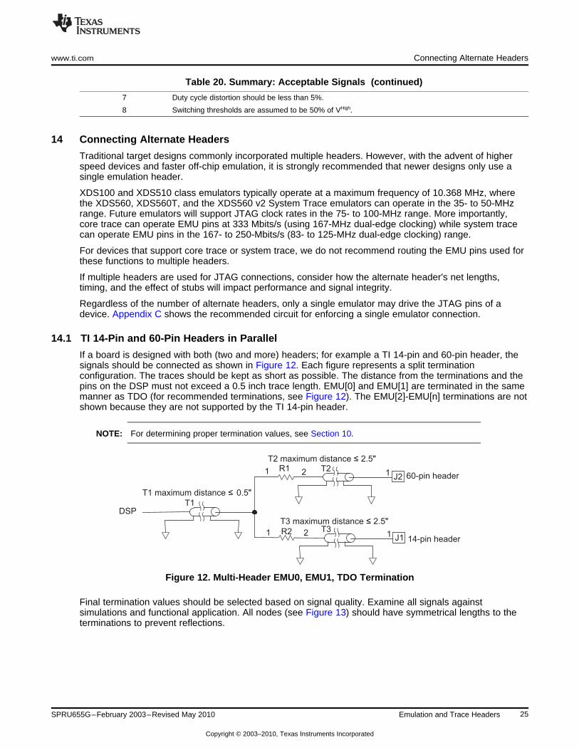
14.1 TI 14-Pin and 60-Pin Headers in Parallel ........................................................................... 25
15 Layout and Routing Requirements ...................................................................................... 2615.1 Maximum Recommended Distances ................................................................................ 26
16 Advanced Emulation - Layout and Route Distance Deviations ................................................ 2816.1 Signal-to-Signal Clearance ........................................................................................... 28
16.2 PWB Routing Lengths ................................................................................................. 28
17 Traditional JTAG Emulation Layout and Route Distance Deviations ........................................ 2917.1 Layout and Routing - Mechanical Considerations ................................................................. 29
18 Multiple Device Considerations ........................................................................................... 3218.1 Multiple-Processor Termination ...................................................................................... 35
Appendix A Alternate Target Impedance Configurations ................................................................ 36Appendix B Buffering - Methods, Techniques and Terminations ..................................................... 37Appendix C TI 14-Pin and 60-Pin Headers in Parallel ..................................................................... 39Appendix D Layout and Routing Requirements ............................................................................. 41
D.1 Layout and Route Deviations [Advanced Emulation] ............................................................ 41
Appendix E XDS560T Spice Model ............................................................................................... 42Appendix F XDS560 v2 System Trace Modeling ............................................................................ 57Appendix G Finding a Buffer's Output Impedance ......................................................................... 59Appendix H Variable Board Impedance ........................................................................................ 61Appendix I Revision History ....................................................................................................... 62
3SPRU655G–February 2003–Revised May 2010 Table of Contents
Copyright © 2003–2010, Texas Instruments Incorporated

www.ti.com
List of Figures
1 TI 60-Pin Emulation Header ............................................................................................. 10
2 MIPI 60-Pin Header ....................................................................................................... 10
3 TI 20-Pin CTI Header ..................................................................................................... 10
4 TI 14-Pin Traditional Through-Hole Emulation Interface ............................................................. 11
5 TI 14-Pin Traditional SMT Emulation Interface Header .............................................................. 11
6 60-Pin Header Orientation ............................................................................................... 17
7 Emulator Cable Connector Superimposed Over 60-Pin Header .................................................... 18
8 MIPI 60-Pin Header Pin Location ....................................................................................... 19
9 TI 20-Pin CTI Header Pin Location ..................................................................................... 19
10 Target Connection for Unbuffered JTAG and EMU Signals ......................................................... 21
11 Acceptable Wave Form Criteria ......................................................................................... 24
12 Multi-Header EMU0, EMU1, TDO Termination ........................................................................ 25
13 Symmetrical Nets.......................................................................................................... 26
14 TI 60-Pin Connector Maximum Trace Length ......................................................................... 27
15 MIPI 60-Pin Connector Maximum Trace Length ...................................................................... 27
16 XDS560T TI 60-Pin Target Cable Connector Minimum Clearance - Height....................................... 29
17 XDS560 v2 System Trace MIPI 60-Pin Target Cable Connector Minimum Clearance - Height ................ 30
18 XDS560T TI 60-Pin Target Cable Header Dimensions .............................................................. 30
19 XDS560 v2 System Trace MIPI 60-Pin Target Cable Header Dimensions........................................ 30
20 XDS560T TI 60-Pin Target Cable Board Keep-Out Area ............................................................ 31
21 XDS560 v2 System Trace MIPI 60-Pin Target Cable Board Keep-Out Area ..................................... 31
22 Multiple Device - Single Trace Configuration .......................................................................... 33
23 Multiple Device - Parallel Trace Configuration......................................................................... 34
24 Device-Independent Trace Configuration .............................................................................. 34
25 Parallel Termination ....................................................................................................... 35
26 Recommended TCK Buffered Configuration........................................................................... 37
27 Recommended TCK Unbuffered Configuration ....................................................................... 37
28 Recommended RTCK Configuration.................................................................................... 37
29 Recommended EMU Output Configuration ............................................................................ 38
30 TCK, Multiple Header Configuration .................................................................................... 39
31 Preferred Configuration for EMU0 and EMU1 Terminations......................................................... 40
32 EMU0 Simulation Model (TI's XDS560T Pod Assembly - 50-Ω and 75-Ω Target and Pod Model) ............ 43
33 EMU0 Acceptable Wave Form (Host Side, TI's XDS560T Pod - 50 Ω) ............................................ 45
34 EMU0 Wave Form (Host Side, TI's XDS560T - 75 Ω)................................................................ 47
35 EMU2 Type Signals Simulation Model (TI's XDS560T Pod Assembly - 50-Ω Target and Pod Model)........ 48
36 EMU2 Type Signals Acceptable Wave Form (Host Side, TI's XDS560T Pod - 50 Ω) ........................... 50
37 EMU18 Type Signals Simulation Model (TI's XDS560T Pod Assembly - 50-Ω Target and Pod Model) ...... 51
38 EMU18 Type Signals - Acceptable Wave Form (Host Side, TI's XDS560T Pod - 50 Ω) ....................... 53
39 EMU0 Dual-Header Simulation Model (TI's XDS560T Pod Assembly - 50-Ω Target and Pod Model) ........ 54
40 EMU0 Dual-Header - Wave Form (Host Side, TI's XDS560T Pod - 50 Ω) ........................................ 56
41 TRCLK[0] Model Schematic.............................................................................................. 58
42 Various PCB Impedance Calculations.................................................................................. 61
43 Example of 10-Layer PCB Construction................................................................................ 61
4 List of Figures SPRU655G–February 2003–Revised May 2010
Copyright © 2003–2010, Texas Instruments Incorporated
www.ti.com
List of Tables
1 Emulation Header Use ..................................................................................................... 8
2 Adapters...................................................................................................................... 9
3 Summary: Alternate Target Impedance Configurations................................................................ 9
4 Summary: TI 60-Pin Header Information ................................................................................ 9
5 Summary: MIPI 60-Pin Header Information ............................................................................. 9
6 Summary: TI 20-Pin CTI Header Information.......................................................................... 10
7 Summary: Header Footprint Comparisons ............................................................................. 11
8 Summary: Header Changes ............................................................................................. 11
9 TI 60-Pin Header Signal Naming Convention ......................................................................... 12
10 Summary: TI 60-Pin Header Pinout..................................................................................... 13
11 MIPI 60-Pin Header Signal Naming Convention ..................................................................... 14
12 TI 20-Pin CTI Header Signal Naming Convention .................................................................... 16
13 Summary: Header Pin Assignments .................................................................................... 16
14 JTAG Signal Directions ................................................................................................... 20
15 Summary: Electrical Requirements ..................................................................................... 22
16 Termination Values and Use Cases .................................................................................... 22
17 Summary: Single-Processor Terminations ............................................................................. 22
18 Summary: Buffering ....................................................................................................... 23
19 General Specifications .................................................................................................... 23
20 Summary: Acceptable Signals ........................................................................................... 24
21 Summary: TI 14-Pin and 60-Pin Headers in Parallel ................................................................. 26
22 Summary: Advanced Emulation Layout and Routing................................................................. 29
23 Summary: Layout and Routing - Mechanical Considerations (TI 60-Pin).......................................... 31
24 Summary: Layout and Routing - Mechanical Considerations (MIPI 60-Pin)....................................... 32
25 Sizing Common Termination Resistor Values ......................................................................... 35
26 EMU Pins Modeled as EMU2 or EMU18............................................................................... 43
27 Buffer Name Decode andOutput Impedance .......................................................................... 59
28 Recommended Series Termination Resistor Value................................................................... 59
29 Model_name Example .................................................................................................... 60
30 Emulation and Trace Headers Revision History....................................................................... 62
5SPRU655G–February 2003–Revised May 2010 List of Tables
Copyright © 2003–2010, Texas Instruments Incorporated

PrefaceSPRU655G–February 2003–Revised May 2010
Read This First
About This Manual
This technical reference describes how to incorporate Texas Instruments' next-generation emulationheader on a board with a trace-enabled DSP.
Notational Conventions
This document uses the following conventions.
• Hexadecimal numbers are shown with the suffix h. For example, the following number is 40hexadecimal (decimal 64): 40h.
• Registers in this document are shown in figures and described in tables.
– Each register figure shows a rectangle divided into fields that represent the fields of the register.Each field is labeled with its bit name, its beginning and ending bit numbers above, and itsread/write properties below. A legend explains the notation used for the properties.
– Reserved bits in a register figure designate a bit that is used for future device expansion.• Measurements are in English standard units (inches, pounds, etc.).
Related Documentation
The following documents describe the TMS320C6000™ DSP platform and related support tools. Copies ofthese documents are available on the Internet at www.ti.com. Tip: Enter the literature number in thesearch box provided at www.ti.com.
SPRA439 — Emulation Fundamentals for TI's DSP Solutions. This paper explains the fundamentals ofhow the emulation logic and emulation tools work together with the TI digital signal processors. Byunderstanding the fundamentals of emulation, you will be able to accelerate the process of settingup and performing software debug, as well as aid in troubleshooting potential problems in thedebugging setup. A detailed explanation of the setup of the emulator hardware systems for singleand multi-processor applications, along with a discussion of how the system components interactduring debug will be discussed in the sections to follow. Also included is a troubleshooting guide toassist in common setup problems.
SPRU641 — TMS320C6000 DSP Designing for JTAG Emulation Reference Guide. This documentassists you in meeting the design requirements of the XDS510™ emulator with respect to JTAGdesigns and discusses the XDS510 cable. This cable supports both standard 3-volt and 5-volttarget system power inputs.
SPRU589 — XDS560 Emulator Reference Guide. This technical reference describes the fundamentalsof the XDS560™ PCI Emulator and Pod and how to interface it to a target system.
SPDU079 — JTAG/MPSD Emulation Technical Reference. A reference guide that provides detailedinformation to be used when designing for JTAG emulation.
SPRAAK6 — Common Trace Transmission Problems and Solutions. This document providesguidelines for identifying and solving common problems associated with the collecting of high speeddata. On a trace-capable device, the trace interface is one of the highest performance interfaces.Although only used during design, development, and debug, the trace interface must beimplemented correctly for full functionality and performance.
6 Preface SPRU655G–February 2003–Revised May 2010
Copyright © 2003–2010, Texas Instruments Incorporated
www.ti.com Related Documentation
IEEE Std 1149.1-1990 — IEEE Std 1149.1-1990 IEEE Standard Test Access Port and Boundary-ScanArchitecture -Description. Circuitry that may be built into an integrated circuit to assist in the test,maintenance, and support of assembled printed circuit boards is defined. The circuitry includes astandard interface through which instructions and test data are communicated. A set of testfeatures is defined, including a boundary-scan register, such that the component is able to respondto a minimum set of instructions designed to assist with testing of assembled printed circuit boards.
TMS320C6000, XDS510, XDS560 are trademarks of Texas Instruments.ARM is a trademark of of ARM Limited in the EU and other countries.
7SPRU655G–February 2003–Revised May 2010 Read This First
Copyright © 2003–2010, Texas Instruments Incorporated

Technical Reference ManualSPRU655G–February 2003–Revised May 2010
Emulation and Trace Headers
1 Introduction
This technical reference describes the requirements necessary to incorporate an emulation header on aboard that includes devices that support trace export through the device's EMU pins to an emulator withtrace capture support, such as the XDS560T. Texas Instruments device's support various combinations ofDSP core trace and system trace. In all cases, the trace data rates require that the EMU pins be treatedas high-speed clocks within your design. This specifically means that the EMU pins must be terminatedproperly and the correct header chosen for the number of EMU pins required. In the case of core trace orif core trace and system trace export are both supported, this requires utilizing a 60-pin header in place ofthe traditional TI 14-pin or TI 20-pin CTI emulation header. In the case where a device only supportsexport of system trace data, a TI 20-pin CTI header may be used.
Core trace typically provides at least processor PC trace, and depending on the silicon implementationmay also provide processor data trace and event trace. System trace is a message-based technologythat, in enabled silicon, can export application instrumentation and hardware generated messages fromsystem-level monitors. Many devices support on-chip embedded trace buffers (ETBs) either exclusively orin combination with support for exporting trace data through the device's EMU pins. In cases where adevice exclusively utilizes an ETB, a 60-pin header is not required to replace the traditional TI 14-pin or TI20-pin CTI headers on the board, but keep in mind that ETBs only allow visibility to shallow snapshots ofdata (typically in the 4K to 32K range). To determine if your device supports exporting core or systemtrace through the EMU pins and/or supports one or multiple ETBs, see the device-specific data sheet. Theadvantage of exporting core and system trace data through the EMU pins to an emulator with tracecapture support, such as the XDS560T, is that the capture depth is much greater (typically many Mbytes),providing a much larger region of visibility and enabling precise profiling and code coverage tooling.
If the device supports any type of core trace export that you want to capture using a TI trace-enabledemulator, then a 60-pin header in place of the traditional TI 14-pin or TI 20-pin CTI TI emulation headers isa requirement. If your device supports only export of system trace data, then you can choose the headerthat fits your needs.
Table 1. Emulation Header Use
Trace Type Emulator Type Native Emulator Header
DSP Core Trace XDS560T TI 60-Pin
System Trace XDS560T TI 60-Pin (1)
System Trace XDS560 v2 System Trace MIPI 60-Pin (1)
(1) Since system trace only utilizes 5 EMU pins, if your processor only supports system trace exportthrough EMU0:4, then you may choose to use a TI-20 pin connector with an adapter.
Even though the 60-pin header supports all the features provided by the original TI 14-pin header, not allemulators, target cables, and target device combinations support all features. To confirm that the desiredfunctionality is supported, see the documentation and device user guides for your specific emulator.
2 Adapters
Adapters allow the XDS560T and XDS560 v2 System Trace emulators to be used with standard TI 14-pinand TI 20-pin CTI target headers, or adaptors can be used to allow a standard XDS100, XDS510, orXDS560 emulator to be used with a target board that is implemented with a TI 60-pin or MIPI 60-pinheader. The adapters, listed in Table 2, are available (or may be available in the future) from TI or its thirdparties.
8 Emulation and Trace Headers SPRU655G–February 2003–Revised May 2010
Copyright © 2003–2010, Texas Instruments Incorporated
www.ti.com Fundamental Information
Table 2. Adapters
For Emulator Type . . . From Emulator To Target Notes
XDS560/XDS510/XDS100 TI 14-Pin TI 60-Pin
XDS560 Rev D TI 20-Pin CTI TI 60-Pin
XDS560T TI 60-Pin TI 14-Pin
XDS560T TI 60-Pin TI 20-Pin CTI Check Availability
XDS560T TI 60-Pin MIPI 60-Pin Check Availability
XDS560T TI 60-Pin TI 60-Pin Pin Saver
XDS560 v2 System Trace MIPI 60-Pin TI 60-Pin Check Availability
XDS560 v2 System Trace MIPI 60-Pin TI 20-Pin CTI Check Availability
NOTE: Use of any adapter can have a negative impact on performance.
3 Fundamental Information
This technical reference offers guidance for creating new designs that take advantage of the extendedemulation capabilities. This document is not intended to be the sole design guide.
In addition to this guide, good engineering practices for high-speed logic design and mechanical layoutmust be followed. Any deviation from such practices and design techniques will affect the end-productperformance.
4 Alternate Target Impedance Configurations
Within specific end-use applications for TI's hardware emulation products, multiple printed circuit board(PCB) trace impedances may be required. The advanced emulation signals connecting to the emulationheader require a 50-Ω trace impedance for optimal performance.
For additional information on DSP target applications that incorporate alternate interfaces including, butnot limited to, PCI or external memory interfaces (EMIF), see Appendix A.
Table 3. Summary: Alternate Target Impedance Configurations
1 Target boards without special considerations must be designed for a 50-Ω character impedance.
2 All header EMU signals must be routed as if they are clock signal lines operating at 200 MHz. TIrecommends designing JTAG signals for 100-MHz operation.
5 Header Information
Table 4, Table 5, and Table 6 summarize the header information. For specific pin assignments, seeSection 8.
Table 4. Summary: TI 60-Pin Header Information
1 Connector Manufacturer is Samtec USA.
2 Connector Model Number is SOLC-115-02-S-Q-P.
3 Connector Specification Overview is located at URLhttp://www.samtec.com/technical_specifications/overview.aspx?series=SOLC.
4 Connector Drawing is located at URL http://www.samtec.com/ftppub/cpdf/SOLC-MKT.PDF
5 Connector Footprint Drawing is located at URL http://www.samtec.com/ftppub/cpdf/SOLC.PDF
Table 5. Summary: MIPI 60-Pin Header Information
1 Connector Manufacturer is Samtec USA.
2 Connector Model Number is QSH030.
3 Connector Specification Overview is located at URLhttp://www.samtec.com/technical_specifications/overview.aspx?series=QSH.
9SPRU655G–February 2003–Revised May 2010 Emulation and Trace Headers
Copyright © 2003–2010, Texas Instruments Incorporated

0.3200"
0.8500"
0.8375"
0.295"
0.50"
0.2960"
Header Footprint Comparisons www.ti.com
Table 5. Summary: MIPI 60-Pin Header Information (continued)
4 Connector Drawing is located at URLhttp://www.samtec.com/ftppub/cpdf/QSH-XXX-01-X-D-XXX-MKT.pdf.
5 Connector Footprint Drawing is located at URLhttp://www.samtec.com/ftppub/cpdf/QSH-XXX-01-X-D-XX-FOOTPRINT.pdf.
Table 6. Summary: TI 20-Pin CTI Header Information
1 Connector Manufacturer is Samtec USA.
2 Connector Model Number is FTR-110-51-S-D-06.
3 Connector Specification Overview is located at URLhttp://www.samtec.com/technical_specifications/overview.aspx?series=FTR.
4 Connector Drawing is located at URL http://www.samtec.com/ftppub/cpdf/FTR-MKT.PDF.
5 Connector Footprint Drawing is located at URL http://www.samtec.com/ftppub/cpdf/FTR-D.PDF.
6 Header Footprint Comparisons
Figure 1 through Figure 3 show TI target connector footprint drawings and Table 7 shows a comparison ofthe board space required for each connector type.
In this case, dimensions include space required for the target cable mating connector.
Figure 1. TI 60-Pin Emulation Header
Figure 2. MIPI 60-Pin Header
Figure 3. TI 20-Pin CTI Header
10 Emulation and Trace Headers SPRU655G–February 2003–Revised May 2010
Copyright © 2003–2010, Texas Instruments Incorporated

13 01
0.1950"
0.7200"
13 01
0.3100"
www.ti.com Target Mating Caution
Figure 4. TI 14-Pin Traditional Through-Hole Emulation Interface
Figure 5. TI 14-Pin Traditional SMT Emulation Interface Header
Table 7. Summary: Header Footprint Comparisons
Area (in squareCommon Emulation Interfaces Notesinches)
1 TI 60-pin 0.2720 in2 Includes mounting pads
2 MIPI 60-pin 0.2471 in2 Includes mounting pads
3 TI 20-pin CTI 0.148 in2 Includes mounting pads
4 20-pin ARM™ ETM header 0.3451 in2 Includes mounting pads
5 Original through-hole TI 14-pin connector form factor 0.2808 in2 Includes both sides of PCB
6 Original TI 14-pin SMT connector form factor 0.2431 in2 Includes mounting pads
7 Target Mating Caution
NOTE: All headers (emulator and target) should be examined for possible damage before beingmated together. Damaged or bent pins may affect functionality and performance.
Never apply excessive force when mating connectors; if excessive force is required, the mating connectorpairs are not aligned.
Table 8. Summary: Header Changes
1 Verify the target and emulator headers are intact and free of defects before mating.
2 Always use caution when mating connectors to ensure no damage occurs.
3 Verify connectors are parallel to one another before mating.
11SPRU655G–February 2003–Revised May 2010 Emulation and Trace Headers
Copyright © 2003–2010, Texas Instruments Incorporated

Header Pin Assignment www.ti.com
8 Header Pin Assignment
Table 9. TI 60-Pin Header Signal Naming Convention
EmulatorPin Signal SignalNo. Name Direction Notes
A1 GND (1) - Ground pin.
A2 GND - Ground pin.
A3 GND - Ground pin.
A4 GND - Ground pin.
A5 GND - Ground pin.
A6 GND - Ground pin.
A7 GND - Ground pin.
A8 TYPE0 Output Type 0 is a No Connect.
A9 GND - Ground pin.
A10 GND - Ground pin.
A11 GND - Ground pin.
A12 GND - Ground pin.
A13 GND - Ground pin.
A14 GND - Ground pin.
A15 TGTRST Output Even though the native TI 60-pin emulator (XDS560T) does not support the target resetfunction, other emulators, such as the XDS560 with the REV D cable do support thisfunction. For compatibility, typically through the use of adapters, with emulators that supportthe target reset function it is recommended that on your target board this pin be pulled upwith a 4.7-KΩ resistor.
B1 ID0 Input Only header type 0000 is currently supported, where 0 is GND and 1 is a No Connect. Allother combinations are reserved.
B2 TMS Output Connect to device pin of same name.
B3 EMU17 (2) Bidirectional Connect to device pin of same name.
B4 TDI Output Connect to device pin of same name.
B5 EMU14 (2) Bidirectional Connect to device pin of same name.
B6 EMU12 (2) Bidirectional Connect to device pin of same name.
B7 TDO Input Connect to device pin of same name.
B8 TVD Input Chip I/O voltage current limited via 100-Ω resistor.
B9 EMU9 (2) Bidirectional Connect to device pin of same name.
B10 EMU7 (2) Bidirectional Connect to device pin of same name.
B11 EMU5 (2) Bidirectional Connect to device pin of same name.
B12 TCK Output Connect to device pin of same name; may need to be buffered.
B13 EMU2 (2) Bidirectional Connect to device pin of same name.
B14 EMU0 (2) Bidirectional Connect to device pin of same name.
B15 ID1 Input Only header type 0000 is currently supported, where 0 is GND and 1 is a No Connect. Allother combinations are reserved.
C1 ID2 Input Only header type 0000 is currently supported, where 0 is GND and 1 is a No Connect. Allother combinations are reserved.
C2 EMU18 (2) Bidirectional Connect to device pin of same name.
C3 TRST Output Connect to device pin of same name.
C4 EMU16 (2) Bidirectional Connect to device pin of same name.
C5 EMU15 (2) Bidirectional Connect to device pin of same name.
(1) On some target applications, detection of the emulation pod is required. It is recommended that when this condition exists, pinA1 on the 60-pin header be used. Instead of grounding pin A1 on the target board, a pull-up resistor ≥ to 10K Ω should beconnected to the pin. When the emulation pod header is connected, pin A1 will be grounded.
(2) The 60-pin header provides 19 EMU pins for advance emulation features. Not all devices support 19 EMU pins. Connect onlythe EMU pins present on the target DSP to the corresponding EMU pin on the header. Leave unused pins unconnected.
12 Emulation and Trace Headers SPRU655G–February 2003–Revised May 2010
Copyright © 2003–2010, Texas Instruments Incorporated

www.ti.com Header Pin Assignment
Table 9. TI 60-Pin Header Signal Naming Convention (continued)
EmulatorPin Signal SignalNo. Name Direction Notes
C6 EMU13 (2) Bidirectional Connect to device pin of same name.
C7 EMU11 (2) Bidirectional Connect to device pin of same name.
C8 TCKRTN Input Connect to either a loopback of the emulation header's TCK or a target device-suppliedRTCK. If your target device has an RTCK signal, you must connect this signal to TCKRTNon the emulator header. (3)
C9 EMU10 (2) Bidirectional Connect to device pin of same name.
C10 EMU8 (2) Bidirectional Connect to device pin of same name.
C11 EMU6 (2) Bidirectional Connect to device pin of same name.
C12 EMU4 (2) Bidirectional Connect to device pin of same name.
C13 EMU3 (2) Bidirectional Connect to device pin of same name.
C14 EMU1 (2) Bidirectional Connect to device pin of same name.
C15 ID3 Input Only header type 0000 is currently supported, where 0 is GND and 1 is a No Connect. Allother combinations are reserved.
D1 NC - Not connected.
D2 GND - Ground pin.
D3 GND - Ground pin.
D4 GND - Ground pin.
D5 GND - Ground pin.
D6 GND - Ground pin.
D7 GND - Ground pin.
D8 TYPE1 Output Type 1 must be connected to GND.
D9 GND - Ground pin.
D10 GND - Ground pin.
D11 GND - Ground pin.
D12 GND - Ground pin.
D13 GND - Ground pin.
D14 GND - Ground pin.
D15 GND - Ground pin.(3) For additional notes, see Table 13.
Table 10. Summary: TI 60-Pin Header Pinout
1 Pin D1 should be left unconnected.
2 Pin A1, if required, enables or disables external multiplexers or buffers.
3 Only the appropriate trace pins should be connected.
13SPRU655G–February 2003–Revised May 2010 Emulation and Trace Headers
Copyright © 2003–2010, Texas Instruments Incorporated

Header Pin Assignment www.ti.com
The MIPI 60-pin header provides for up to four channels of independently clocked trace data, where thefirst channel of data can span up to 40 bits, the second channel can span up to 20 bits, and the third andforth channels can span up to 10 bits each. By overlaying the channel bit mapping, multiple configurationsare provided such as four 10-bit ports, two 20-bit ports, or a 32-bit port and an 8-bit port. Since TI traceenabled emulators currently only support a single channel of data, the mapping to TI devices is currentlyfor a single port. Future emulators may require a different mapping so always check the latest revision ofthis document before starting a new design using the MIPI 60-pin header.
The MIPI 60-pin connector also provides two level-dependent nTRST signals and trace and JTAGindependent voltage references.
Note that not all TI devices use the EMU pin naming convention for designating trace pins. Devices thatexport only an ARM ETM trace port have a trace clock, trace control, and trace data pins. Typical pindesignators are ETK_NAME and ETMNAME (where NAME is some variation of CLK, CNTL, and DATA).When connecting an ARM ETM port to the MIPI connector, trace clock is connected to TRC_CLK[0], tracecontrol is connected to TRC_DATA[0][0], and trace data is connected to TRC_DATA[0][1] toTRC_DATA[0][n]. If your device has a trace clock-in pin, leave it disconnected or pull it up externally toincrease noise immunity over the internal pull-up. Check with your emulator manufacturer on availability ofARM ETM trace support.
Table 11. MIPI 60-Pin Header Signal Naming Convention (1) (2) (3)
Pin No. MIPI Name Device Signal Name Notes
1 VREF_DEBUG JTAG IO Vref JTAG IO voltage referencecurrent limited via 100-Ωresistor.
2 TMS/TMSC TMS
3 TCK TCK May need to be buffered.
4 TDO/EXTA TDO
5 TDI/EXTB TDI
6 nRESET Connect to system reset Open drain output fromemulator; use 4.7-KΩ PU. (3)
7 RTCK/EXTC RTCK Connect to either a loopback ofthe emulation header's TCK or atarget device-supplied RTCK. Ifyour target device has an RTCKsignal, you must connect thissignal to RTCK on the emulatorheader. (3)
8 nTRST_PD nTRST It is expected that this pin beconnected only to devices withinternal PDs on their nTRSTpins, or in cases where a PD isrequired externally on thedevice's nTRST pin (for PDinformation and requirements,see your device's data sheet). (4)
9 nTRST/EXTD nTRST nTRST is an open drain output.It is expected that this pin beconnected only to devices withinternal PUs on their nTRSTpins, or in cases where a PU isrequired externally on thedevice's nTRST pin (for PUinformation and requirements,see your device's data sheet). (4)
10 EXTE/TRIGIN NC
11 EXTF/TRIGOUT NC
(1) The QSH-030 connector also has an additional 4 pins (61, 62, 63 and 64) used to connect the cable's ground shield to the targetboards ground plane.
(2) Leave unused TRC_DATA and TRC_CLK pins unconnected.(3) For additional notes, see Table 13.(4) A device may be connected to either nTRST or nTRST_PD, not both at the same time.
14 Emulation and Trace Headers SPRU655G–February 2003–Revised May 2010
Copyright © 2003–2010, Texas Instruments Incorporated

www.ti.com Header Pin Assignment
Table 11. MIPI 60-Pin Header Signal Naming Convention (1) (2) (3) (continued)
Pin No. MIPI Name Device Signal Name Notes
12 VREF_TRACE EMU IO Vref EMU IO voltage referencecurrent limited via 100-Ωresistor.
13 TRC_CLK[0] EMU2
14 TRC_CLK[1] NC
15 Target Presence Detect Connected to GND thru 0 Ω16 GND GND
17 TRC_DATA[0][0] EMU3
18 TRC_DATA[1][0] or TRC_DATA[0][20] NC
19 TRC_DATA[0][1] EMU0
20 TRC_DATA[1][1] or TRC_DATA[0][21] NC
21 TRC_DATA[0][2] EMU1
22 TRC_DATA[1][2] or TRC_DATA[0][22] NC
23 TRC_DATA[0][3] EMU4
24 TRC_DATA[1][3] or TRC_DATA[0][23] NC
25 TRC_DATA[0][4] EMU5
26 TRC_DATA[1][4] or TRC_DATA[0][24] NC
27 TRC_DATA[0][5] EMU6
28 TRC_DATA[1][5] or TRC_DATA[0][25] NC
29 TRC_DATA[0][6] EMU7
30 TRC_DATA[1][6] or TRC_DATA[0][26] NC
31 TRC_DATA[0][7] EMU8
32 TRC_DATA[1][7] or TRC_DATA[0][27] NC
33 TRC_DATA[0][8] EMU9
34 TRC_DATA[1][8] or TRC_DATA[0][28] NC
35 TRC_DATA[0][9] EMU10
36 TRC_DATA[1][9] or TRC_DATA[0][29] NC
37 TRC_DATA[3][0] or TRC_DATA[0][10] EMU11
38 TRC_DATA[2][0] or TRC_DATA[1][10] or NCTRC_DATA[0][30]
39 TRC_DATA[3][1] or TRC_DATA[0][11] EMU12
40 TRC_DATA[2][1] or TRC_DATA[1][11] or NCTRC_DATA[0][31]
41 TRC_DATA[3][2] or TRC_DATA[0][12] EMU13
42 TRC_DATA[2][2] or TRC_DATA[1][12] or NCTRC_DATA[0][32]
43 TRC_DATA[3][3] or TRC_DATA[0][13] EMU14
44 TRC_DATA[2][3] or TRC_DATA[1][13] or NCTRC_DATA[0][33]
45 TRC_DATA[3][4] or TRC_DATA[0][14] EMU15
46 TRC_DATA[2][4] or TRC_DATA[1][14] or NCTRC_DATA[0][34]
47 TRC_DATA[3][5] or TRC_DATA[0][15] EMU16
48 TRC_DATA[2][5] or TRC_DATA[1][15] or NCTRC_DATA[0][35]
49 TRC_DATA[3][6] or TRC_DATA[0][16] EMU17
50 TRC_DATA[2][6] or TRC_DATA[1][16] or NCTRC_DATA[0][36]
51 TRC_DATA[3][7] or TRC_DATA[0][17] EMU18
15SPRU655G–February 2003–Revised May 2010 Emulation and Trace Headers
Copyright © 2003–2010, Texas Instruments Incorporated

Header Pin Assignment www.ti.com
Table 11. MIPI 60-Pin Header Signal Naming Convention (1) (2) (3) (continued)
Pin No. MIPI Name Device Signal Name Notes
52 TRC_DATA[2][7] or TRC_DATA[1][17] or NCTRC_DATA[0][37]
53 TRC_DATA[3][8] or TRC_DATA[0][18] EMU19
54 TRC_DATA[2][8] or TRC_DATA[1][18] or NCTRC_DATA[0][38]
55 TRC_DATA[3][9] or TRC_DATA[0][19] NC
56 TRC_DATA[2][9] or TRC_DATA[1][19] or NCTRC_DATA[0][39]
57 GND GND
58 GND GND
59 TRC_CLK[3] NC
60 TRC_CLK[2] NC
Table 12. TI 20-Pin CTI Header Signal Naming Convention
Pin No. Signal Name Notes
1 TMS
2 TRST
3 TDI
4 TDIS (1) Connect to target GND.
5 VTRef JTAG and EMU IO voltage reference current limited via 100-Ω resistor.
6 KEY This pin may need to be cut to mate with the emulator's target cable.
7 TDO
8 GND
9 RTCK Connect to either a loopback of the emulation header's TCK or a targetdevice-supplied RTCK. If your target device has an RTCK signal, youmust connect this signal to RTCK on the emulator header. (2)
10 GND
11 TCK May need to be buffered.
12 GND
13 EMU0
14 EMU1
15 RESET Open drain output from emulator, use 4.7-KΩ PU. (2)
16 GND
17 EMU2
18 EMU3
19 EMU4
20 GND(1) A pulldown or current-limiting resistor on TDIS will not work with all XDS models. With TDIS connected directly to GND, some
XDS models will sink a small amount of current (by design) through a pullup in the XDS. A pulldown or a current-limiting resistorconnected to TDIS on the target may cause the XDS to not detect the target and result in a "far cable break" error.
(2) For additional notes, see Table 13.
Table 13. Summary: Header Pin Assignments
1 EMU0 and EMU1 should always be treated as bidirectional signals. For bidirectional debug portfunctions, check your device data sheet. Other EMU pins may also be bidirectional, but typically they areused for unidirectional core and system trace export.
2 If your target card contains multiple devices with RTCK pins see the Adaptive Clock article athttp://tiexpressdsp.com/index.php/Adaptive_Clocking.
16 Emulation and Trace Headers SPRU655G–February 2003–Revised May 2010
Copyright © 2003–2010, Texas Instruments Incorporated
B1A1B2A2B3A3B4A4B5A5B6A6B7A7B8A8B9A9
B10A10B11A11B12A12B13A13B14A14B15A15
D1C1D2C2D3C3D4C4D5C5D6C6D7C7D8C8D9C9D10C10D11C11D12C12D13C13D14C14D15C15
Towardsedge
of board(cable entry)
Towardsdevice
www.ti.com Header Pin Assignment
Table 13. Summary: Header Pin Assignments (continued)
3 The TGTRST, nRESET, and RESET signals are open drain outputs that can be integrated into yourcard's POR circuit, in which case (if supported by the emulator), it may allow you to reset your entireboard through the emulator. This feature is supported by the XDS560 with the rev. D cable and theXDS560 v2 System Trace emulator. The XDS560T does not support this feature.
Figure 6 is a top view of Texas Instruments' 60-pin emulation header, illustrating the orientation and pinlocation of the 60-pin emulation header. For specific pin assignments, see Table 9. Texas Instruments'emulation and debug pod incorporates a pin 1 (red dot) locator on the emulation and debug pod(Figure 7). Alignment with the pin 1 of the target board header is critical.
Figure 6. 60-Pin Header Orientation
17SPRU655G–February 2003–Revised May 2010 Emulation and Trace Headers
Copyright © 2003–2010, Texas Instruments Incorporated

Edge of Board
Towardsdevice
A1
Y
20
Pin 1 Location onemulation pod (red dot)
Side 1 Location onemulation header
Header Pin Assignment www.ti.com
Figure 7. Emulator Cable Connector Superimposed Over 60-Pin Header
18 Emulation and Trace Headers SPRU655G–February 2003–Revised May 2010
Copyright © 2003–2010, Texas Instruments Incorporated

1
5
9
13
17
21
25
29
33
37
41
45
49
53
57
3
7
11
15
19
23
27
31
35
39
43
47
51
55
59
2
6
10
14
18
22
26
30
34
38
42
46
50
54
58
4
8
12
16
20
24
28
32
36
40
44
48
52
56
60
Towardsedge
of board(cable entry)
Towardsdevice
1
3
5
7
9
11
13
15
17
19
2
4
6
8
10
12
14
16
18
20
www.ti.com Header Pin Assignment
Figure 8 and Figure 9 are top views of the MIPI 60-pin and TI 20-pin CTI emulation headers, respectively.These illustrations show the orientation and pin location of the emulation headers.
Note:
• The QSH-030 connector also has an additional 4 pads; one of which, at a minimum, must be used to connect thecable's ground shield to the target boards ground plane.
• The QSH-030 connector is keyed so unlike the TI-60 connector there is no way to install it backwards.
Figure 8. MIPI 60-Pin Header Pin Location
Note: Pin 6 may need to be cut to mate with the emulator's target cable.
Figure 9. TI 20-Pin CTI Header Pin Location
19SPRU655G–February 2003–Revised May 2010 Emulation and Trace Headers
Copyright © 2003–2010, Texas Instruments Incorporated

Electrical Requirements www.ti.com
9 Electrical Requirements
This section describes the basic electrical requirements. Deviation from these requirements may result inperformance degradation.
Table 14 defines the chip pin input pull-up and pull-down characteristics.
Table 14. JTAG Signal Directions
Signal Name DSP Direction Notes
EMU[N] (1) Bidirectional Pull-up within device per device data sheet
TCK (2) In Pull-up within device per device data sheet
TDI (2) In Pull-up within device per device data sheet
TDO Out Pull-up within device per device data sheet
TMS (2) In Pull-up within device per device data sheet
TRST (2) In Pull-down within device per device data sheet(1) Varies by device type, see the device data sheet for actual number of EMU pins.(2) Internal device pull-ups and pull-downs are typically weak (~30K Ω). Your application may require stronger external pull-ups or
pull-downs to improve noise margins on the JTAG input signals (TMS, TDI, TCK, TRST) and EMU signals when an emulationcable is not connected.
In cases where your target board contains a single device that is connected to the emulation header andthe emulation header is positioned within 3" of the target device, Figure 10 shows the basic connection forunbuffered signals.
20 Emulation and Trace Headers SPRU655G–February 2003–Revised May 2010
Copyright © 2003–2010, Texas Instruments Incorporated

Target Device
EMU0
EMU1
EMU2
EMUn
EMU0/TRC_DATA[0][1]
EMU1/TRC_DATA[0][2]
EMU2/TRC_CLK[0]
EMUn/TRC_DATA[0][m](F)
Board Power
CVDD
4.7K W
TDI
TDO
TMS
TDI
TDO
TMS
DVDD
EMU series
termination resistors(A)
100- current-
limiting resistor
W(B)
TVD/VREF_DEBUGVREF_TRACE/VTRef
Targetvoltage source
Target IOvoltage source
TDO series
termination resistor(A)
Emulation Header
TGTRST RESET/
22 W(E)
TCK
RTCK22 W
TCK
TCK
RTCKRTCK
22 W(E)
TCK
nTRST nTRST/nTRST_PD(G)
(D)
JTAG Clock
Configuration 1(C)
JTAG Clock
Configuration 2(D)
DVDDDVDD
4.7K W(I)
4.7KW(H)
4.7KW(H)
www.ti.com Electrical Requirements
Note: All routing distances from the device pins to the emulation header must be less than 3 inches.
A To select EMU and TDO series termination resistor values, see Section 10. The EMU and TDO series terminationvalues should be placed within 0.5" of the device with total routing length not to exceed 3".
B If using a MIPI 60-pin connector, VREF_DEBUG and VREF_TRACE provide independent voltage sources for JTAGand EMU pins.
C If your target device does not have an RTCK pin, loopback TCK is supplied by the emulation header to RTCK perConfiguration 1.
D If your device supports an RTCK pin, then connect the device's RTCK to the emulation header's RTCK perConfiguration 2 and follow the instructions in Note A to size and place RTCK's series termination resistor.
E On JTAG signals that are inputs to the device, place 22-Ω series termination resistors in close proximity to theemulation header.
F For the MIPI 60-pin header the mapping between EMU and TRC_DATA signals is not one-to-one. For the correctEMU to MIPI 60-pin mapping, see Table 11.
G If using the MIPI 60-pin connector, see Table 11 for notes on nTRST and nTRST_PD use.
H Pull-ups on EMU0 and EMU1 may be optional. For cases where external pull-ups are required or should beconsidered, see the XDS Target Connection Guide. If you decide pull-ups are needed on EMU0 and EMU1 keep thelength of the trace route from the EMU pin to the pull-up to a minimum.
I A pull-down on nTRST may be optional. For cases where an external pull-down is required or should be considered,see the XDS Target Connection Guide.
Figure 10. Target Connection for Unbuffered JTAG and EMU Signals
21SPRU655G–February 2003–Revised May 2010 Emulation and Trace Headers
Copyright © 2003–2010, Texas Instruments Incorporated

Single-Processor Termination www.ti.com
Table 15. Summary: Electrical Requirements
1 Always refer to the device data sheet for number and connectivity of EMU pins.
2 Leave unused EMU pins unconnected.
10 Single-Processor Termination
The information provided in this section applies to a single-processor system. For multi-processorconfigurations, see Section 18.
Current emulators operate the JTAG's clock in the 10-MHz to 50-MHz range, but future emulators willoperate at higher clock rates. Thus, to provide some design margin for duty cycle distortion andcompatibility with future emulators, TI recommends designing JTAG signals for 100-MHz operation.
Core trace currently operates with transfer rates as high 333 Mbits/sec, with 167-MHz DDR clocking andrise and fall times in the 250-1000 picoseconds range. System trace operates with transfer rates of 250Mbits/s with 125-MHz DDR clocking. To provide some design margin for duty cycle distortion, TIrecommends designing EMU signals for trace as 200-MHz clock signals.
The following termination information assumes that the impedance of the PCB traces from the DSP to theemulation header is controlled and is between 50 and 55 Ω. The ideal series termination resistor value fora single device connected to any EMU or JTAG output signal is determined by the following equation:
ZCable - ZDevice_Output = ZTermination_Resistor
The impedance of the XDS560T and XDS560 V2 System Trace cables is 50 Ω.
Follow the guidelines in Table 16 to determine the placement and size of series termination resistors forthe JTAG and EMU signals on your target board. For output pins you will need to know the impedance ofthe pin's buffer. To determine this, see Appendix G.
Table 16. Termination Values and Use Cases
Signal Name Notes
TDO Must be placed as close as possible to the pin on the device, not to exceed 1" trace length from the pin.Since TDO is a device output, use the equation ZCable - ZDevice_Output = ZTermination_Resistor to determine theproper termination resistor value.
TCKRTN/RTCK If your device does not have an RTCK pin and the TCKRTN/RTCK signal is not buffered, this signal isrouted from the emulation header's TCK with a 22-Ω series resistor using a routing length as short aspossible. If your device has an RTCK pin and the TCKRTN/RTCK signal is not buffered, this signal isrouted from the device's RTCK with a series termination resistor, sized using the equation ZCable -ZDevice_Output = ZTermination_Resistor and using a routing length as short as possible. If TCKRTN/RTCK isbuffered, see Figure 26; if unbuffered, see Figure 27; and if there is a direct connection to the device'sRTCK, see Figure 28.
TCK 100 Ω in series with 8.2-pF parallel termination to ground for buffered TCK configuration (Figure 26).Use a 22-Ω series termination (near header) for unbuffered configuration (Figure 27). Values should bemodeled to ensure proper value.
EMU[N:2] Must be placed as close as possible to the EMU pin on the device, placement should not exceed 1"trace length from the pin at the DSP (see Figure 29). To determine the proper termination resistor value,use the equation ZCable - ZDevice_Output = ZTermination_Resistor.
EMU[1:0] Must be placed as close as possible to the EMU pin on the device, placement should not exceed 1"(0.5" recommended) trace length from the pin of the DSP. If a TI 14-pin header is used in parallel, aseparate series termination resistor must be used to route these signals to the TI 14-pin header, seeFigure 31. To determine the proper termination resistor value, use the equation ZCable - ZDevice_Output =ZTermination_Resistor.
For additional information on the trace lengths and impact of termination location, see Section 16 andAppendix B.
Table 17. Summary: Single-Processor Terminations
1 Use of termination resistors on JTAG device output signals and EMU pins used for core trace or systemtrace required.
2 Alternate termination values should be used if indicated by detailed modeling.
3 Model all critical nets to ensure termination values are correct.
22 Emulation and Trace Headers SPRU655G–February 2003–Revised May 2010
Copyright © 2003–2010, Texas Instruments Incorporated
www.ti.com Buffering
Table 17. Summary: Single-Processor Terminations (continued)
4 Placement of indicated terminations is critical.
11 Buffering
If buffers are used, they should be selected based on the device source impedance and the potentialload(s). In applications where multiple devices are used, selection of buffers and signals to be buffered arecritical.
When buffering signals, it is imperative that timing, propagation delay, sink and source currents, andgeneral buffer characteristics be considered.
See Appendix B for additional information on the buffering, location, and type of buffers to be used.
Table 18. Summary: Buffering
1 Buffer signals based on loading and signal integrity.
2 In most cases, a single target board is better than a target board with daughter cards consisting ofmultiple headers.
3 Timing is a critical consideration for all active signals.
4 Model all critical nets to ensure termination values are correct.
12 General Specifications
General specifications are shown in Table 19.
Table 19. General Specifications
Item Description/Specification
Impedance Target board impedance should be in the range of 50 Ω (±5Ω).
Connector Spacing Maximum distance from header pin to respective emulation pin on DSP equals 3.0-inch trace length.
Signal Skew For EMU signals, skew induced by the board should be 200 ps maximum between signals.
Capacitance Maximum capacitance loading per pin (inclusive of all vias and components) equals 20 pF.
Signal Interconnect Number of vias, not more than 2, and must be within the capacitive loading specified above.
Clock Source The emulator must be provided a clock source through the header's TCKRTN or RTCK pin. For boardrequirement details, see Section 8 and Section 9.
Voltage Source TVD (TI 60-pin header), VREF_DEBUG and VREF_TRACE (MIPI 60-pin header), and VTRef (TI20-pin CTI header) require a current-limited customer-supplied voltage reference source.
Voltage Range The XDS560T is designed to operate between 0.8 V to 5.0 V. The XDS560 v2 System Trace emulatoris designed to operate in the 1.2-V to 3.3-V range.
Orientation Detect The MIPI 60-pin header is self-aligning and cannot be installed backwards. The TI 20-pin CTIconnector uses pin 6 as an orientation key that may need to be removed. On the TI 60-pin connectorpin A8 is a NC; pin D8 must be connected to GND.
Vertical Connector For TI 60-pin connector clearance, see Figure 16; for the MIPI 60-pin connector clearance, seeClearance Figure 17.
Horizontal Connector Clearance surrounding the TI 60-pin emulator connector should be per Figure 18 and Figure 20.Clearance Clearance surrounding the MIPI 60-pin header should be per Figure 19 and Figure 21.
Signal Frequency EMU signals should be designed to operate as 200-MHz clocks and JTAG signals should bedesigned to operate at 100 MHz.
Rise and Fall times All rising and falling edges are assumed to be within 500-1500 picoseconds.
13 Acceptable Signal Qualifications
The criteria for determining an acceptable signal waveform during simulation at the emulator's input bufferor in actual application are illustrated in Figure 11. All percentages listed are with respect to the VHigh
reference levels ( LVTTL 3.3 V).
23SPRU655G–February 2003–Revised May 2010 Emulation and Trace Headers
Copyright © 2003–2010, Texas Instruments Incorporated
A
B
C
D
E
F
G
H
+120%
+100%
+80%
+70%
+50%
+30%
+20%
0%
-20%
VHigh
VHigh Good
VLow Good
Acceptable Signal Qualifications www.ti.com
A Details the maximum amount of reflection, or perturbations that may occur on the rising edge (pre-shoot). Themagnitude of the reflections or perturbations should be less than 20% of VHigh.
B Details the critical signal switching region. No inflections greater than 10% of the rise time or 5% greater than VHigh areallowed. It is preferred that the signal be able to increase monotonically.
C Details the region of the rising edge above the critical signal switching area. Inflections and/or perturbations areallowed within this region as long as they do not exceed 20% of VHigh or a duration less than the rise time of the pulse.
D Details the top of the pulse. The amplitude of all noise, crosstalk and other perturbations should be less than 10% ofVHigh. For a 3.3 V signal, the amplitude should not exceed 165 mV.
E Details the maximum amount of reflection, or perturbations that may occur on the falling edge. The magnitude of thereflections or perturbations should be less than 20% of VHigh.
F Details the critical signal-switching region. No inflections greater than 10% of the fall time or 5% greater than VHigh areallowed. It is preferred that the signal be able to decrease monotonically.
G Details the region of the falling edge below the critical signal switching area. Inflections and/or perturbations areallowed within this region as long as they do not exceed 20% of VHigh or a duration less than the fall time of the pulse.
H Details the bottom of the pulse. The amplitude of all noise, crosstalk and other perturbations should be less than 10%of VHigh.
• Duty cycle distortion should be less than 5%.• All waveforms should be treated as dual edge clocks.• Rise and fall times should be symmetrical.• Switching thresholds are assumed to be 50% of VHigh.
Figure 11. Acceptable Wave Form Criteria
Table 20. Summary: Acceptable Signals
1 Calculate reflections to verify they will not fall within the switching regions.
2 Perturbations should not exceed 20% of VHigh.
3 Rise and fall times should be symmetrical.
4 The duration of overshoots should not exceed 20% of VHigh or less than the rise time of the pulse.
5 Noise and crosstalk should not exceed 10% of VHigh or 165 mV for a 3.3 V signal.
6 All wave forms should be treated as dual edge clocks.
24 Emulation and Trace Headers SPRU655G–February 2003–Revised May 2010
Copyright © 2003–2010, Texas Instruments Incorporated
T1 maximum distance 0.5≤ "
T1DSP
R11 2
1 R2 2
T2
T3
J2
J1
60-pin header
14-pin header
T2 maximum distance 2.5≤ "
1
1
T3 maximum distance 2.5≤ "
www.ti.com Connecting Alternate Headers
Table 20. Summary: Acceptable Signals (continued)
7 Duty cycle distortion should be less than 5%.
8 Switching thresholds are assumed to be 50% of VHigh.
14 Connecting Alternate Headers
Traditional target designs commonly incorporated multiple headers. However, with the advent of higherspeed devices and faster off-chip emulation, it is strongly recommended that newer designs only use asingle emulation header.
XDS100 and XDS510 class emulators typically operate at a maximum frequency of 10.368 MHz, wherethe XDS560, XDS560T, and the XDS560 v2 System Trace emulators can operate in the 35- to 50-MHzrange. Future emulators will support JTAG clock rates in the 75- to 100-MHz range. More importantly,core trace can operate EMU pins at 333 Mbits/s (using 167-MHz dual-edge clocking) while system tracecan operate EMU pins in the 167- to 250-Mbits/s (83- to 125-MHz dual-edge clocking) range.
For devices that support core trace or system trace, we do not recommend routing the EMU pins used forthese functions to multiple headers.
If multiple headers are used for JTAG connections, consider how the alternate header's net lengths,timing, and the effect of stubs will impact performance and signal integrity.
Regardless of the number of alternate headers, only a single emulator may drive the JTAG pins of adevice. Appendix C shows the recommended circuit for enforcing a single emulator connection.
14.1 TI 14-Pin and 60-Pin Headers in Parallel
If a board is designed with both (two and more) headers; for example a TI 14-pin and 60-pin header, thesignals should be connected as shown in Figure 12. Each figure represents a split terminationconfiguration. The traces should be kept as short as possible. The distance from the terminations and thepins on the DSP must not exceed a 0.5 inch trace length. EMU[0] and EMU[1] are terminated in the samemanner as TDO (for recommended terminations, see Figure 12). The EMU[2]-EMU[n] terminations are notshown because they are not supported by the TI 14-pin header.
NOTE: For determining proper termination values, see Section 10.
Figure 12. Multi-Header EMU0, EMU1, TDO Termination
Final termination values should be selected based on signal quality. Examine all signals againstsimulations and functional application. All nodes (see Figure 13) should have symmetrical lengths to theterminations to prevent reflections.
25SPRU655G–February 2003–Revised May 2010 Emulation and Trace Headers
Copyright © 2003–2010, Texas Instruments Incorporated

T1 maximum distance 0.5"≤
T1DSP
R11 2
1 R2 2
Symmetricallengths
Layout and Routing Requirements www.ti.com
Figure 13. Symmetrical Nets
Table 21. Summary: TI 14-Pin and 60-Pin Headers in Parallel
1 The series termination closest to the DSP should be closer than 0.50".
2 Traces originating at nodes should have symmetrical lengths.
3 The maximum distance originating from the node to the respective header should not exceed 1.5" inlength.
4 Final termination values must be based on simulation and functional testing.
5 All terminations and nets should be void of stubs.
15 Layout and Routing Requirements
15.1 Maximum Recommended Distances
The layout requires certain specifications. Figure 14 illustrates the maximum recommended routingdistance between the header pin and respective DSP EMU (emulation trace) pin. All emulation signalsshould be treated as a separate net class and routed accordingly. Take special care to meet the skewspecifications. Figure 14 shows a TI 60-pin connector orientation to a device such that the device'sfarthest EMU pin is no more than 3" from the corresponding header pin. Figure 15 shows a MIPI 60-pinconnector orientation. In both figures the orientation provides for a left side cable entry.
26 Emulation and Trace Headers SPRU655G–February 2003–Revised May 2010
Copyright © 2003–2010, Texas Instruments Incorporated

3 maximumtrace length"
B1A1B2A2B3A3B4A4B5A5B6A6B7A7B8A8B9A9
B10A10B11A11B12A12B13A13B14A14B15A15
D1C1D2C2D3C3D4C4D5C5D6C6D7C7D8C8D9C9D10C10D11C11D12C12D13C13D14C14D15C15
Red highlighted pin is the farthestEMU pin from the connector.
3" maximumtrace length
Red highlighted pin is the farthestEMU pin from the connector.
1
5
9
13
17
21
25
29
33
37
41
45
49
53
57
3
7
11
15
19
23
27
31
35
39
43
47
51
55
59
2
6
10
14
18
22
26
30
34
38
42
46
50
54
58
4
8
12
16
20
24
28
32
36
40
44
48
52
56
60
www.ti.com Layout and Routing Requirements
Figure 14. TI 60-Pin Connector Maximum Trace Length
Note: Orient the pin 1 side of the MIPI 60-pin connector to the target device or devices.
Figure 15. MIPI 60-Pin Connector Maximum Trace Length
27SPRU655G–February 2003–Revised May 2010 Emulation and Trace Headers
Copyright © 2003–2010, Texas Instruments Incorporated

Advanced Emulation - Layout and Route Distance Deviations www.ti.com
16 Advanced Emulation - Layout and Route Distance Deviations
16.1 Signal-to-Signal Clearance
Consider routing key emulation or clock signals when laying out your target board with respect to theemulation header. The potential for signal noise, crosstalk, and coupling increases with the high frequencyof TI's trace-enabled emulators. To minimize this variable, route all clock and emulation (EMU) signalswith a minimum of a 5 mil (0.005") clearance, although 6 mil (0.006") is preferred.
16.2 PWB Routing Lengths
Regardless of the configuration (for configuration descriptions, see Section 18), the maximumrecommended PWB routing length between a processor's EMU pin and the corresponding EMU pin on thetarget connector should be no more than 3". For multiple processor configurations, EMU0 and EMU1 maybe used for global breakpoints and as cross triggers between devices that are in the JTAG scan chain butmay or may not be connected for core or system trace. In this case, you may need to exceed therecommended maximum routing length when using an EMU pin for cross triggers or global breakpoints,possibly making these pins unusable for trace. In this case, core trace and system trace can typically bededicated to EMU pins not used for global breakpoints or cross triggers by either shifting trace to thehigher order EMU pins (if supported by your device) or by reducing the number of pins used for tracewhich, in turn, reduces the bandwidth available for trace. If your device supports more than 12 EMU pins,then shifting trace to higher-order bits may be an option, otherwise reducing the number of pins availablefor trace may be your only option.
PWB routing length considerations take on two key variables: propagation and skew.
Propagation involves the distance between the header and the respective pin on the DSP. ExcessivePWB routing lengths present a problem, specifically with reflections. The key to minimizing the impact ofreflections is to minimize PWB routing lengths. When possible, lay out critical signals such that theypropagate between the insertion and terminating points in a period of time that does not result in thereflected energy occurring in the switching region or the additive effect of multiple reflections does not fallin the switching regions on either the rising or falling edge. All active PWB routing lengths (specifically foremulation, JTAG, and clock signals) should not exceed 3 inches in length. Lengths in excess of 3 inchesincrease the risk of reflections occurring in the critical regions of the signal waveform.
The remaining PWB routing length variable is signal skew. For the purposes of this document, signal skewis the difference between the minimum and maximum propagation delays (Tpd) for a net class (grouping ofsignals belonging together). In most high-speed applications, such as TI's trace supported emulators,skew is as important as propagation delays. TI's trace supported emulators accommodate a certainamount of skew; however, excessive skew greater than 200 ps (or 1.1" for FR4) introduced during layoutand routing may reduce performance.
Excessive skew or propagation delays increase the risk in potential bit errors, loss of data or faultyoperation. Figure 14 and Figure 15 illustrate the recommended header distance from the target processor.
While considering the routed length implications of propagation and skew, also consider the total circuit.Most traditional board designers are concerned with only the routes on their board. However, the targetboard is only one of three critical components of the typical emulation system. The interconnecting podassembly and emulator are the other critical components. Consider all three components when designinga high-speed functional system.
The advanced emulation pins from the DSP to the header are grouped and routed as a net class toconstrain the skew for all EMU[0] through EMU[n] signals. Emulation signals on the target board must beshort because of the timing constraints. The distance for the EMU[n] net class of signals can also beinterpreted as a maximum routed distance of 3 inches; this is inclusive of all supporting logic in eachsignal path on the target board.
Appendix E and Appendix F provide models representing the XDS560T and XDS560 v2 System Traceinterconnect logic. Deviations from the recommended route distances, loading, or skew must be evaluatedusing the representative model to ensure optimum frequency operation and overall performance.
28 Emulation and Trace Headers SPRU655G–February 2003–Revised May 2010
Copyright © 2003–2010, Texas Instruments Incorporated

0.274 max"
0.556"
www.ti.com Traditional JTAG Emulation Layout and Route Distance Deviations
Table 22. Summary: Advanced Emulation Layout and Routing
1 All high speed emulation signals (CLKS and EMU) should be spaced a minimum of 5 mil from othersignals.
2 PWB routing lengths for all clock and EMU signals should not exceed 3" maximum.
3 Skew between signals within a net class should not exceed 200 ps.
4 Layout and routing should also take into account the emulator and target.
5 PWB routing should have a character impedance of 50 Ω.
17 Traditional JTAG Emulation Layout and Route Distance Deviations
Layout and routing considerations include traditional JTAG signals, such as TDI, TDO, TMS, TCK, andTCKRTN/RTCK. The greater the distance (or skew) between the header and the target processor, thegreater the potential for timing errors (set up and hold, etc.). Skewing routed signals such as TCK andTDI, or TDO and TCKRTN/RTCK, dramatically reduces the margin of setup timing to and from the targetprocessor. Figure 14 and Figure 15 illustrate the recommended header distance from the target processor.
As with the advanced emulation features described above, the routed length is equally, if not moreimportant. Traditional JTAG signals, especially in the interconnecting pod, may serve other purposes infuture devices. The interconnecting pod assembly has a significant amount of support logic that contains alarge portion of the allotted quota of the routed distance. That, coupled with the induced cable propagationdelay, requires that the traditional JTAG emulation signals be short.
As stated previously, traditional board designers typically concern themselves with only the routes on theboard they are designing. The basic emulation signals are critical, not because of their high speed, butbecause of their unique timing characteristics. As the TCK and TCKRTN/RTCK rates increase, the marginfor setup and hold times decrease, so both must be considered when designing a high speed functionalsystem.
The distance for the traditional JTAG emulation signals is inclusive of all supporting logic in each signalpath on the target board. A model representing the pod interconnect logic is provided in Appendix E forthe TI 60-pin cable and Appendix H for the MIPI 60-pin cable. Deviations from the recommended routedistances, loading, or skew must be evaluated using this representative model to ensure optimumfrequency operation and overall performance.
NOTE: Follow routing guideline for best operating frequency
Failure to follow the above routing guideline may result in a severely reduced operatingfrequency, resulting in lost bandwidth or the inability of the advanced features to function atfull speed.
17.1 Layout and Routing - Mechanical Considerations
In addition to routing and layout considerations and electrical clearances, certain mechanical clearancesmust be observed and followed.
Figure 16. XDS560T TI 60-Pin Target Cable Connector Minimum Clearance - Height
29SPRU655G–February 2003–Revised May 2010 Emulation and Trace Headers
Copyright © 2003–2010, Texas Instruments Incorporated

0.292"
0.725"
1.700" minimum
clearance to cable bend
1.230"
1.060"
0.775"
1.175"1.075"
Traditional JTAG Emulation Layout and Route Distance Deviations www.ti.com
Figure 17. XDS560 v2 System Trace MIPI 60-Pin Target Cable Connector Minimum Clearance - Height
Figure 18 and Figure 19 illustrate the top view of the emulation and debug pod header enclosure;additional spacing is required for installing and removing the pod target connector and for clearance of theemulator cable assembly.
Figure 18. XDS560T TI 60-Pin Target Cable Header Dimensions
Figure 19. XDS560 v2 System Trace MIPI 60-Pin Target Cable Header Dimensions
The TI 60-pin target cable clearance area includes optional space on each side of the connector forgriping the connector (see Figure 20). Given the connector housing is 0.274" off of the plane of the board,this space may be used by components that do not exceed the 0.274" height without impacting the abilityto install or remove the connector.
30 Emulation and Trace Headers SPRU655G–February 2003–Revised May 2010
Copyright © 2003–2010, Texas Instruments Incorporated

0.8500"
0.4500²
0.3200"
0.1330"
0.900"
0.5800"
0.4200"
0.8800"
Keep-out area
0.8375²
0.300²
0.295²
0.880²
1.128²
Keep-out area
0.560²
www.ti.com Traditional JTAG Emulation Layout and Route Distance Deviations
Figure 20. XDS560T TI 60-Pin Target Cable Board Keep-Out Area
Table 23. Summary: Layout and Routing - Mechanical Considerations (TI 60-Pin)
1 The maximum height of components in the keep-out area cannot exceed 0.274".
2 The basic area of concern beneath the pod header is 1.8" × 1.33".
The MIPI 60-pin target cable clearance area includes optional space on each side of the connector forgriping the connector (see Figure 21). Given the cable's adapter board is 0.292" off of the plane of theboard, this space may be used by components that do not exceed the 0.292" height without impacting theability to install or remove the connector.
Figure 21. XDS560 v2 System Trace MIPI 60-Pin Target Cable Board Keep-Out Area
For mechanical specifications that may deviate from this guide, see your specific emulator manufacturer’sdocumentation.
31SPRU655G–February 2003–Revised May 2010 Emulation and Trace Headers
Copyright © 2003–2010, Texas Instruments Incorporated

Multiple Device Considerations www.ti.com
Table 24. Summary: Layout and Routing - Mechanical Considerations (MIPI 60-Pin)
1 The maximum height of components in the keep-out area cannot exceed 0.292".
2 The basic area of concern beneath the pod header is 1.76" × 1.428".
18 Multiple Device Considerations
There are three supported multiple device configurations: single trace, independent trace, and paralleltrace. The single trace configuration allows for multiple devices to be connected to the JTAG serial scanchain, but only a single device connected to the emulation connector's EMU pins for trace support. Usethis configuration if you are only interested in trace data from a single device or if the EMU signal routingto the other devices exceed the recommended lengths. Independent trace requires an emulation socketper device and should be utilized in cases where you need to observe trace from multiple sourcessimultaneously (using multiple emulators) or if the distance between processors and the emulationconnector exceeds the recommended routing lengths. Parallel trace allows up to four devices to beconnected to the emulation header's EMU pins for trace as long as the longest EMU signal route does notexceed the maximum recommended length while allowing additional devices to be connected to the serialscan chain. Any combination of these configurations may be deployed within a system as long as there isa single independent serial JTAG scan chain per emulation connector.
Figure 22 illustrates the basic single trace device interconnection method. This configuration supportsglobal breakpoints and cross triggering using EMU0 and EMU1 routed in parallel between all processors.It also supports synchronous execution control by daisy-chaining the JTAG signals between processors,and advanced emulation capabilities with EMU[2:n] for a single processor. If the routing lengths for EMU0and EMU1 exceed 3", they may not be usable for trace. For more details on EMU pin and trace options,see Section 16.2, PWB Routing Lengths. Given the source current capability of the individual devices, amaximum of 30 devices on the JTAG serial scan chain or for parallel routing of EMU0 and EMU1 shouldnot be exceeded. Exceeding this number of devices may severely impact performance. When designingtarget systems with a large number of devices, always minimize the number of vias and trace lengths, andpay special attention to the lengths of individual trace stubs. For more information on sizing terminationresistors, see Section 10.
Figure 22, Figure 23, and Figure 24 do not show RTCK. The header's RTCK signal must be connected onthe target per the instructions in Section 8, Header Pin Assignment. For multiprocessor configurations thatcontain devices with RTCK, see Table 13 note 2.
32 Emulation and Trace Headers SPRU655G–February 2003–Revised May 2010
Copyright © 2003–2010, Texas Instruments Incorporated

DSP0 DSP1 DSPn
TDO
TDI
EMU0
EMU2:nTDI-TDO TDI-TDO
TCK,
TMS,
TRST
EMU1
EMU0
TCK,
TMS,
TRST
EMU1
www.ti.com Multiple Device Considerations
Figure 22. Multiple Device - Single Trace Configuration
Figure 23 illustrates the parallel trace configuration. You may connect up to four processors to the sameemulation header pins in parallel, but the current TI trace products will force you to select a single deviceto capture trace data from. Also, keep in mind that if you want to use EMU0 and EMU1 for globalbreakpoints and cross triggers with more than four devices in the serial scan chain, these pins may not beusable for core or system trace pins. For more details on EMU pin and trace options, see Section 16.2,PWB Routing Lengths. For termination instructions for the parallel trace configuration, see Section 18.1.
As with the single trace configuration, the parallel trace configuration also supports synchronous executionand debug visibility to additional devices by daisy-chaining the JTAG signals between processors. Thesame 30-device restriction also applies to this configuration.
33SPRU655G–February 2003–Revised May 2010 Emulation and Trace Headers
Copyright © 2003–2010, Texas Instruments Incorporated

DSP0 DSP1 DSPn
TDO
TDI
EMU0:1
TCK,
TMS,
TRST
EMU2:n TDI-TDO TDI-TDO
EMU0:1
DSP2
TDI-TDO
DSP3
TDI-TDO
TCK,
TMS,
TRST
DSP0 DSPn
TDO
EMU0:n
TCK, TMS,
TRST
TDI
DSP1
TDO
EMU0:n
TCK, TMS,
TRST
TDI
TDO
EMU0:n
TCK, TMS,
TRST
TDI
Multiple Device Considerations www.ti.com
Figure 23. Multiple Device - Parallel Trace Configuration
Figure 24 illustrates the basic independent device interconnection method. Under the independentinterconnection method, each device has its own independent emulation pins assigned per header. Anindependent configuration as indicated in Figure 24 minimizes the pin count efficiency but maximizes theperformance. For more information on sizing termination resistors, see Section 10.
In the illustrated independent configuration (Figure 24), each device is in its own scan chain. Synchronousexecution, cross triggers, and global breakpoints are not supported. Connecting EMU0 and EMU1between devices in this configuration would allow cross triggers to operate, but if routes are long it couldmake the pins unusable for trace.
Figure 24. Device-Independent Trace Configuration
For all configurations, it is vital to both core and system trace that the routing length restrictions(Section 17.1) and termination requirements (Section 10 and Section 18.1) be followed.
34 Emulation and Trace Headers SPRU655G–February 2003–Revised May 2010
Copyright © 2003–2010, Texas Instruments Incorporated

Emulation
Header
0.50"
CPU0/EMUn
CPU1/EMUn
CPU2/EMUn
CPU3/EMUn
2.25"
www.ti.com Multiple Device Considerations
18.1 Multiple-Processor Termination
If you are using the parallel trace configuration (see Figure 25), you may connect each EMU pin used forcore trace or system trace from the emulation connector to no more than four processors. In thisconfiguration, we recommend that each processor have an independent termination resistor whose routingdistance from the processor to the termination resistor does not exceed 0.5", the stubs betweentermination resistors should be as short as possible, the distance between the termination resistors andthe emulation connector do not exceed 2.25", and a total route length from the processor to the emulationconnector of 3" or less. Other configurations may work, but you would need to model the configuration tovalidate.
Figure 25. Parallel Termination
Special consideration must be given to sizing the termination resistors because of the additional parallelimpedances contributed by the combination of the termination resistors and additional EMU pins. It isrecommended you establish the termination value as if a single processor was being used (seeSection 10) and then divide that value between the number of processors connected to the EMU pin of theemulator header. Table 25 should be used for sizing common termination resistor values.
Table 25. Sizing Common Termination Resistor Values
If Single TerminationValue is: 2 Processors 3 Processors 4 Processors
42 20 10 10
33 16 10 10
24 12 10 10
It is not recommended to use termination resistor values lower than 10 Ω or not to use terminationresistors if the value determined is smaller than 10. Use 10 Ω as a minimum.
35SPRU655G–February 2003–Revised May 2010 Emulation and Trace Headers
Copyright © 2003–2010, Texas Instruments Incorporated
www.ti.com
Appendix A Alternate Target Impedance Configurations
Most TI devices are designed to operate on a 50 Ω character impedance target board. For TexasInstruments' devices incorporating a built-in PCI, Ethernet, or memory interface, the trace impedanceshould also be 50 Ω. Other devices may require a different trace impedance in the range of 60 to 100 Ω.
Always see the device application reports or data sheets for detailed impedance requirements and confirmthat the target board is designed accordingly.
Appendix H provides information to assist target board designers in obtaining the optimal interconnectimpedance by varying widths of the appropriate traces. Various constraints are noted, such as thedielectric constant of the board material, the separation between layers, etc. This chart assumes an Er of4.1, which is typical for FR-4 material. This appendix also shows how to design a multiple impedanceprinted circuit board.
36 Alternate Target Impedance Configurations SPRU655G–February 2003–Revised May 2010
Copyright © 2003–2010, Texas Instruments Incorporated

DSP TCK
Emulation headerTCKRTN/RTCK
<2.5"
0.5"
33 W
33 W
74LVC1G32
100 W
8.2 pF
0.5"Emulationheader TCK
10k W
VIO
(A)
Emulation header
TCKRTN/RTCK
3.0" max
1”
22 W
22 W
Emulation
header
TCK
DSP TCK
DSP TCK
DSP RTCK
3.0" max
1" max
22 W
(A)
Emulationheader TCK
Emulation header
TCKRTN/RTCK
www.ti.com
Appendix B Buffering - Methods, Techniques and Terminations
Figure 26 represents the recommended buffering for TCK; alternate buffers may be used if appropriate.To confirm timing, drive, and voltage characteristics for your specific target, see the manufacturer's datasheets.
A JTAG IO voltage level.
Figure 26. Recommended TCK Buffered Configuration
Figure 27 represents the recommended termination for an unbuffered TCK line. Termination values shouldbe placed in close proximity to the emulation header. This configuration should not be used if your devicehas an RTCK pin.
Figure 27. Recommended TCK Unbuffered Configuration
Figure 28 represents the recommended termination for a device that has an RTCK pin. Terminationvalues should be placed in close proximity to the emulation header. The total routing distance for the TCKor RTCK signals between the device and the emulation header should not exceed 3".
A The RTCK series termination resistor is sized using the equation ZCable - ZDevice_Output = ZTermination_Resistor. The seriestermination resistor should be placed as close to the device as possible with the total route not exceeding 3". Foradditional information on determining proper series termination values, see Section 10.
Figure 28. Recommended RTCK Configuration
37SPRU655G–February 2003–Revised May 2010 Buffering - Methods, Techniques and Terminations
Copyright © 2003–2010, Texas Instruments Incorporated

DSP0.5" 2.5"
Emulation
header
Appendix B www.ti.com
Figure 29 illustrates the preferred placement for all emulation (EMU) terminations. Values and placementsmay vary depending on your device and trace lengths. Always model or simulate your design for optimalperformance. For more information on sizing EMU termination resistors, see Section 10.
For additional recommendations, see your device data sheet.
Figure 29. Recommended EMU Output Configuration
Figure 26 and Figure 29 recommend a maximum 0.5" trace distance between the device and thetermination resistor. The distance for this node under all conditions cannot exceed 1.0".
38 Buffering - Methods, Techniques and Terminations SPRU655G–February 2003–Revised May 2010
Copyright © 2003–2010, Texas Instruments Incorporated

DSPTCK
TCKRTN_602.5"
2.5"
33 W
33 W
74LVC1G32
100 W
8.2 pF
0.5"TCK(TI 60-pinorMIPI 60-pin header)
FETSW/mux
TCKRTN_142.5"
33 W
74LVC1G32
0.5" TCK(TI 14-pin orTI 20-pin CTI header)
TI 14-pin orTI 20-pin CTI header
(pin 8, GND)(A)
100 W
8.2 pF
TI 60-pin
header (pin A1, GND)or
(A)
(A)
MIPI 60-pin
header (pin 16, GND)
33 W
10k W
VIO
(B)
10k W
VIO
(B)
10k W
VIO
(B)
10k W
VIO
(B)
www.ti.com
Appendix C TI 14-Pin and 60-Pin Headers in Parallel
If a multi-header configuration is used, the TCK signal must be buffered. For recommended terminations,see Figure 30. The use of an FET style switch or multiplexer, such as a 74CBT3125 or 74CBT3257, ismandatory to minimize clock skew between TCKRTN and the TCK to the DSP.
The buffer, in this case a 74LVC1G32, is not mandatory, any suitable device can be used. The ACterminations and buffers must be located within 0.5-inch trace length of the header. The 33-Ω seriestermination should be located as close as possible to the buffer.
Designers should model their circuits including board impedance to determine the proper terminationvalues.
A Active low cable-present signals are formed. The cable-present signal can also be used with the FET switch's OEpins.
B JTAG IO voltage level.
Figure 30. TCK, Multiple Header Configuration
Figure 31 illustrates the preferred placement for EMU0 and EMU1 terminations when multiple headers areused. Values and placements may vary depending on your device and trace lengths. The trace lengthslisted are maximum values. Always model or simulate your design for optimal performance. For moreinformation on sizing termination resistors, see Section 10 and Appendix G.
For additional recommendations, see your device data sheet.
39SPRU655G–February 2003–Revised May 2010 TI 14-Pin and 60-Pin Headers in Parallel
Copyright © 2003–2010, Texas Instruments Incorporated

DSP0.5" 2.5"42 W 60-pin
header
2.5"42 W 14-pinheader
Appendix C www.ti.com
Figure 31. Preferred Configuration for EMU0 and EMU1 Terminations
Figure 31 recommends a maximum 0.5" trace distance between the device and the termination resistor.The distance for this node under all conditions cannot exceed 3".
40 TI 14-Pin and 60-Pin Headers in Parallel SPRU655G–February 2003–Revised May 2010
Copyright © 2003–2010, Texas Instruments Incorporated

www.ti.com
Appendix D Layout and Routing Requirements
D.1 Layout and Route Deviations [Advanced Emulation]
To minimize routing deviations, provide a clean electrical environment for advance emulation capabilities.The greater the distance (or skew) between the header and the target processor, the greater the potentialfor timing errors. A small amount of skew is acceptable and can be accommodated. However, excessivepropagation or skew, beyond an allotted amount, will produce bit errors, loss of data or faulty operation.The recommended header distance from the target processor is 3 inches maximum.
Models representing the target interconnect are provided in Appendix E and Appendix F for the XDS560Tand XDS560 v2 System Trace emulators.
41SPRU655G–February 2003–Revised May 2010 Layout and Routing Requirements
Copyright © 2003–2010, Texas Instruments Incorporated

www.ti.com
Appendix E XDS560T Spice Model
NOTE:• The models provided are for spice simulation. TI recommends using tools that support
simulating with IBIS models of the TI device and the LVDS buffer (SN65LVDS388A)rather than using the ideal voltage source shown in the following models.
• The models shown use Tran0 and Tran1 values that match the timing diagramsprovided. When performing modeling of your system, you should replace these valueswith your actual values. TI does not recommend exceeding 3" between Tran0 andTran1.
Figure 32 illustrates the EMU0 spice model for TI's XDS560T pod assembly and partial target board logic.
Example 1 is the spice net list for the spice model in Figure 32 . This illustration references a 50-Ωcharacteristic-impedance target PCB. Clock speeds are 200 MHz. Constraints to consider or modify aretrace length and board supporting logic. Additional modeling should be done for signal cross talk.
Figure 33 illustrates an acceptable waveform for Figure 32 and Example 1 using TI's XDS560T and a50-Ω character-impedance target board.
Example 2 illustrates the spice net list used to create the spice model for a 75-Ω target board impedanceand TI's XDS560T pod.
Figure 34 illustrates the waveform for Figure 32 and Example 2 using TI's XDS560T and a 75-Ωcharacter-impedance target board.
Figure 35 illustrates the EMU2 type signals (see Table 26) spice model for TI's XDS560T pod assemblyand partial target board logic.
Example 3 is the spice net list for the spice model in Figure 35. This illustration references a 50-Ωcharacter-impedance target PCB. Clock speeds are 200 MHz. Constraints to consider or modify are tracelength and board supporting logic. Additional modeling should be done for signal cross talk.
Figure 36 illustrates an acceptable waveform for Figure 35 and Example 3 using TI's XDS560T and a50-Ω character-impedance target board.
Figure 37 illustrates the EMU18 type signals (see Table 26) spice model for TI's XDS560T pod assemblyand partial target board logic.
Example 4 is the spice net list for the spice model in Figure 37. This illustration references a 50-Ωcharacter-impedance target PCB. Clock speeds are 200 MHz. Constraints to consider or modify are tracelength and board supporting logic. Additional modeling should be done for signal cross talk.
Figure 38 illustrates an acceptable waveform for Figure 37 and Example 4 using TI's XDS560T and a50-Ω character-impedance target board.
Figure 39 illustrates the dual header configuration EMU0 spice model for TI's XDS560T pod assembly anda partial target board logic. This model is provided to emphasize the advantages of using a singleemulation header.
Example 5 is the spice net list for the spice model in Figure 39. This illustration references a 50-Ωcharacter-impedance target PCB. Clock speeds are 200 MHz. Constraints to consider or modify are tracelength and board supporting logic. Additional modeling should be done for signal cross talk.
Figure 40 illustrates the waveform for Figure 39 and Example 5 using TI's XDS560T and a 50-Ω characterimpedance target board in a two-header configuration.
Certain characteristics of the target board may change - the spice net list must be modified and rerun todetermine the outcome.
42 XDS560T Spice Model SPRU655G–February 2003–Revised May 2010
Copyright © 2003–2010, Texas Instruments Incorporated

Tran0
0.5”C0
0.5 p
Via R1
42
0.5 p
Via
C1
Tran1
1.5”
DSP totermination
Terminationto header
Seriesresistor
1 p
C2
Header N-1header
Tran2
0.5”
PCBtermination
0.5 p
Via
C4
Tran3
5.625”
Cableassembly
0.5 p
Via
C12
Tran4
0.576”
Trace
0.6”trace
Tran5
Tran6
1.3658”trace-via
U23-resistor
0.5
p C7
R3
100 K27
R218
C6 4p
R100100 K
3p C131.3
p C14Tran10
0.7”ESD
termination
2.87 KR216
U23 FET switch
U40 (Comparator)
ESD diode Via-U40
+
TREF_buffer 3.3 V Termination R215
1.5 KR217
0.5
pC
10
1.5 KR214
0.5
pC
9 C503.9 p
V2
Via
DSP - header
XDS560T EMU0
Pod header DSP output60-pin headerinput LVDS
1.5 K
+ V1
DSP
5 p
C11
LVDS
100 K
R8
InputLVDS
www.ti.com Appendix E
Table 26. EMU Pins Modeled as EMU2 or EMU18
Model as EMU2 Model as EMU18
EMU2 EMU12
EMU3 EMU14
EMU4 EMU15
EMU5 EMU16
EMU6 EMU17
EMU7 EMU18
EMU8
EMU9
EMU10
EMU11
EMU13
Figure 32 is a representative spice model for TI's XDS560T pod assembly. Clock speeds are 200 MHz.This illustration supports both a 75-Ω and 50-Ω character-impedance target PCB. Constraints to consideror modify are trace length and board supporting logic. Additional modeling should be done for signal crosstalk.
Figure 32. EMU0 Simulation Model (TI's XDS560T Pod Assembly - 50-Ω and 75-Ω Target and Pod Model)
43SPRU655G–February 2003–Revised May 2010 XDS560T Spice Model
Copyright © 2003–2010, Texas Instruments Incorporated
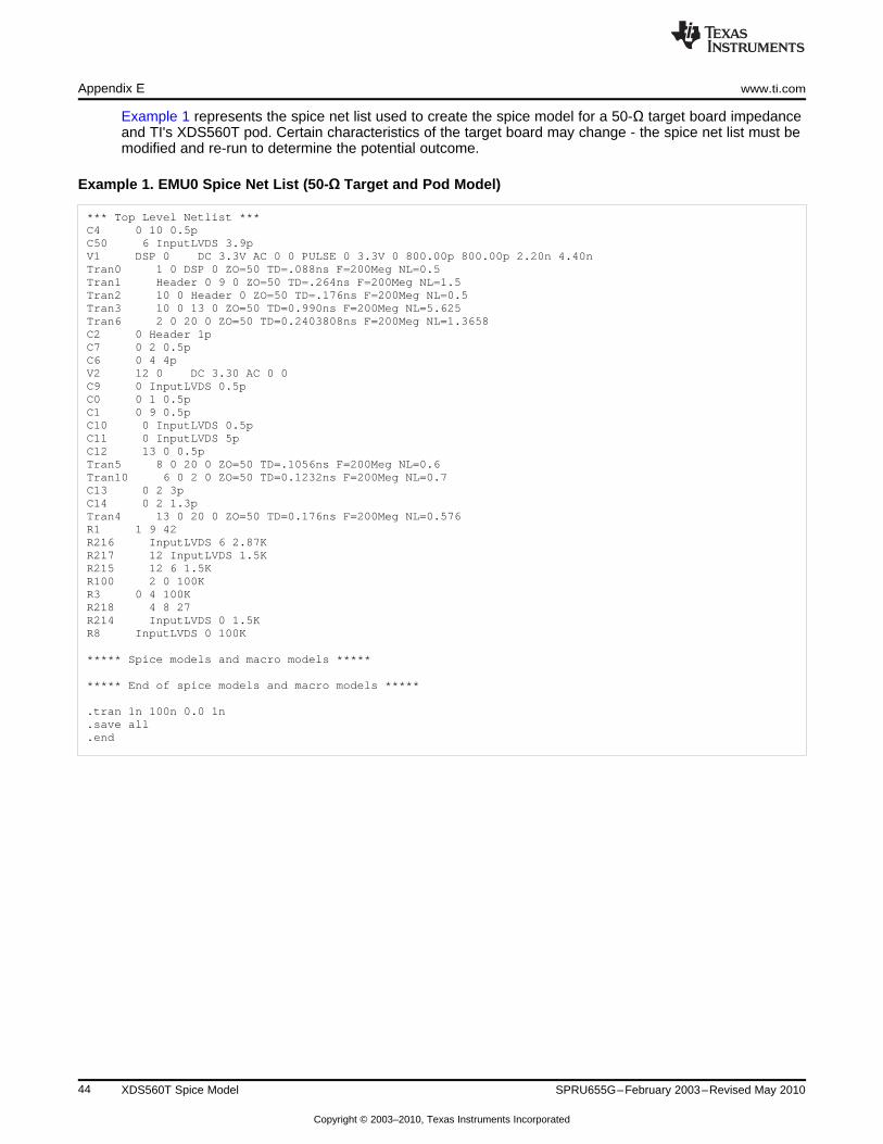
Appendix E www.ti.com
Example 1 represents the spice net list used to create the spice model for a 50-Ω target board impedanceand TI's XDS560T pod. Certain characteristics of the target board may change - the spice net list must bemodified and re-run to determine the potential outcome.
Example 1. EMU0 Spice Net List (50-Ω Target and Pod Model)
*** Top Level Netlist ***C4 0 10 0.5pC50 6 InputLVDS 3.9pV1 DSP 0 DC 3.3V AC 0 0 PULSE 0 3.3V 0 800.00p 800.00p 2.20n 4.40nTran0 1 0 DSP 0 ZO=50 TD=.088ns F=200Meg NL=0.5Tran1 Header 0 9 0 ZO=50 TD=.264ns F=200Meg NL=1.5Tran2 10 0 Header 0 ZO=50 TD=.176ns F=200Meg NL=0.5Tran3 10 0 13 0 ZO=50 TD=0.990ns F=200Meg NL=5.625Tran6 2 0 20 0 ZO=50 TD=0.2403808ns F=200Meg NL=1.3658C2 0 Header 1pC7 0 2 0.5pC6 0 4 4pV2 12 0 DC 3.30 AC 0 0C9 0 InputLVDS 0.5pC0 0 1 0.5pC1 0 9 0.5pC10 0 InputLVDS 0.5pC11 0 InputLVDS 5pC12 13 0 0.5pTran5 8 0 20 0 ZO=50 TD=.1056ns F=200Meg NL=0.6Tran10 6 0 2 0 ZO=50 TD=0.1232ns F=200Meg NL=0.7C13 0 2 3pC14 0 2 1.3pTran4 13 0 20 0 ZO=50 TD=0.176ns F=200Meg NL=0.576R1 1 9 42R216 InputLVDS 6 2.87KR217 12 InputLVDS 1.5KR215 12 6 1.5KR100 2 0 100KR3 0 4 100KR218 4 8 27R214 InputLVDS 0 1.5KR8 InputLVDS 0 100K
***** Spice models and macro models *****
***** End of spice models and macro models *****
.tran 1n 100n 0.0 1n
.save all
.end
44 XDS560T Spice Model SPRU655G–February 2003–Revised May 2010
Copyright © 2003–2010, Texas Instruments Incorporated

www.ti.com Appendix E
The result of your 50-Ω target PCB simulation and modeling should be an acceptable waveform, similar tothat illustrated in Figure 33.
Figure 33. EMU0 Acceptable Wave Form (Host Side, TI's XDS560T Pod - 50 Ω)
45SPRU655G–February 2003–Revised May 2010 XDS560T Spice Model
Copyright © 2003–2010, Texas Instruments Incorporated
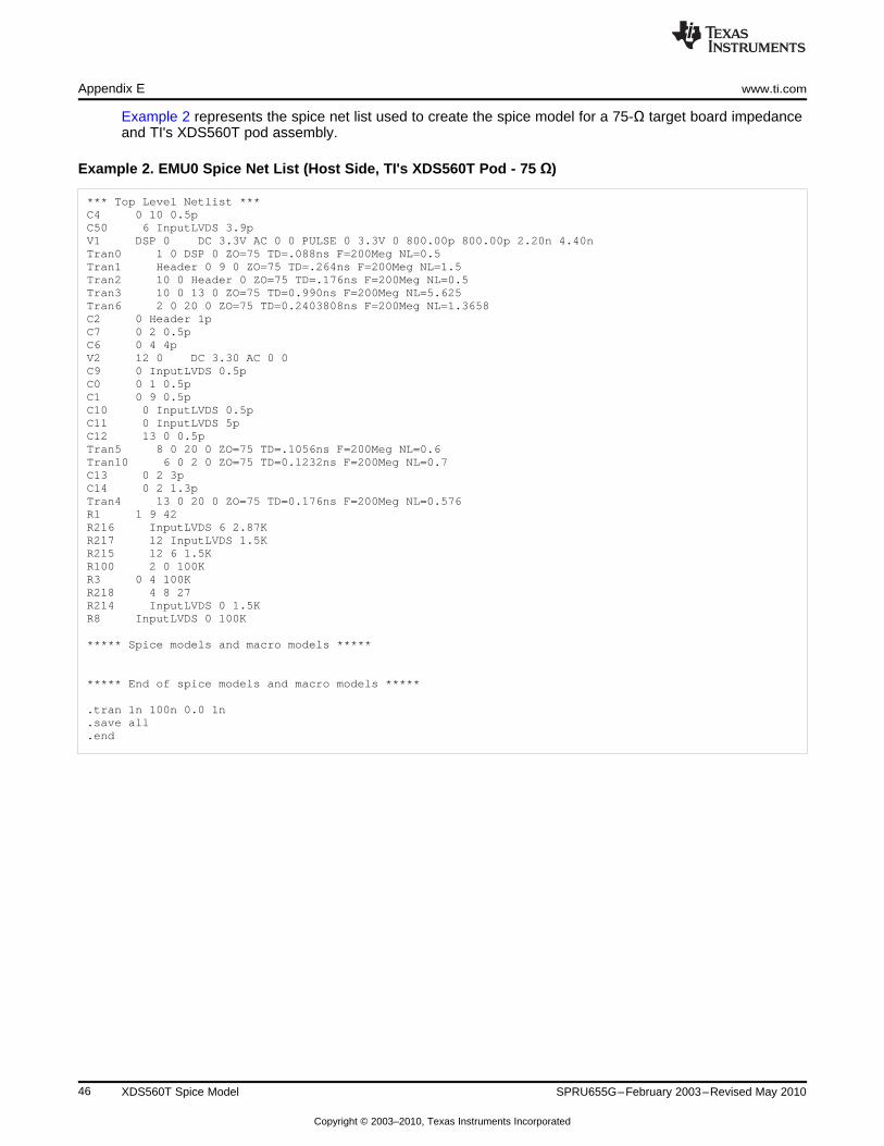
Appendix E www.ti.com
Example 2 represents the spice net list used to create the spice model for a 75-Ω target board impedanceand TI's XDS560T pod assembly.
Example 2. EMU0 Spice Net List (Host Side, TI's XDS560T Pod - 75 Ω)
*** Top Level Netlist ***C4 0 10 0.5pC50 6 InputLVDS 3.9pV1 DSP 0 DC 3.3V AC 0 0 PULSE 0 3.3V 0 800.00p 800.00p 2.20n 4.40nTran0 1 0 DSP 0 ZO=75 TD=.088ns F=200Meg NL=0.5Tran1 Header 0 9 0 ZO=75 TD=.264ns F=200Meg NL=1.5Tran2 10 0 Header 0 ZO=75 TD=.176ns F=200Meg NL=0.5Tran3 10 0 13 0 ZO=75 TD=0.990ns F=200Meg NL=5.625Tran6 2 0 20 0 ZO=75 TD=0.2403808ns F=200Meg NL=1.3658C2 0 Header 1pC7 0 2 0.5pC6 0 4 4pV2 12 0 DC 3.30 AC 0 0C9 0 InputLVDS 0.5pC0 0 1 0.5pC1 0 9 0.5pC10 0 InputLVDS 0.5pC11 0 InputLVDS 5pC12 13 0 0.5pTran5 8 0 20 0 ZO=75 TD=.1056ns F=200Meg NL=0.6Tran10 6 0 2 0 ZO=75 TD=0.1232ns F=200Meg NL=0.7C13 0 2 3pC14 0 2 1.3pTran4 13 0 20 0 ZO=75 TD=0.176ns F=200Meg NL=0.576R1 1 9 42R216 InputLVDS 6 2.87KR217 12 InputLVDS 1.5KR215 12 6 1.5KR100 2 0 100KR3 0 4 100KR218 4 8 27R214 InputLVDS 0 1.5KR8 InputLVDS 0 100K
***** Spice models and macro models *****
***** End of spice models and macro models *****
.tran 1n 100n 0.0 1n
.save all
.end
46 XDS560T Spice Model SPRU655G–February 2003–Revised May 2010
Copyright © 2003–2010, Texas Instruments Incorporated

www.ti.com Appendix E
The result of your 75-Ω target PCB simulation and modeling from Example 2 should be similar to thewaveform illustrated in Figure 34.
Figure 34. EMU0 Wave Form (Host Side, TI's XDS560T - 75 Ω)
47SPRU655G–February 2003–Revised May 2010 XDS560T Spice Model
Copyright © 2003–2010, Texas Instruments Incorporated

Tran0
+ V1
DSP
0.5”C0
0.5 p
Via R1
42
0.5 p
Via
C1
Tran1
1.5”
DSP totermination
Terminationto header
Series termination resistor
1 p
C2
Header N-1header
Tran2
0.5”
PCBtermination
0.5 p
Via
C4
Tran3
5.625”
Cableassembly
Tran4
1.10”
Trace
1.4”
Tran5
0.5
p
C7
Via
1.3
p
C142.87 K
R228
ESD diode
+
3.3 VTREF_buffer
1.5 K
5 p
C11
LVDS
100 K R8
InputLVDS
0.5
pC
10
1.5 KR229
C53
0.5
p C523.9 p
V2
Via
DSP - header
XDS560T EMU2
Pod header
DSP output60-pin header
LVDS input
0.5
p
C120.6”
ESD fortermination
Tran6
Trace-via
Termination
Via
1.5 KR226
Via
R227
Appendix E www.ti.com
Figure 35 is a representative spice model for TI's XDS560T pod assembly. Clock speeds are 200 MHz.This illustration supports a 50-Ω character-impedance target PCB. Constraints to consider or modify aretrace length and board supporting logic. Additional modeling should be done for signal cross talk.
Figure 35. EMU2 Type Signals Simulation Model (TI's XDS560T Pod Assembly - 50-Ω Target and PodModel)
48 XDS560T Spice Model SPRU655G–February 2003–Revised May 2010
Copyright © 2003–2010, Texas Instruments Incorporated

www.ti.com Appendix E
Example 3 represents the spice net list used to create the spice model in Figure 35 for a 50-Ω targetboard impedance and TI's XDS560T pod.
Example 3. EMU2 Type Signals Spice Net List (Host Side, TI's XDS560T Pod - 50 Ω)
*** Top Level Netlist ***C4 0 10 0.5pC52 2 InputLVDS 3.9pV1 DSP 0 DC 3.3V AC 0 0 PULSE 0 3.3V 0 1.00n 1.00n 1.50n 5.00nTran0 1 0 DSP 0 ZO=50 TD=.088ns F=200Meg NL=0.5Tran1 Header 0 9 0 ZO=50 TD=.264ns F=200Meg NL=1.5Tran2 10 0 Header 0 ZO=50 TD=.176ns F=200Meg NL=0.5Tran3 10 0 13 0 ZO=50 TD=0.990ns F=200Meg NL=5.625Tran5 17 0 3 0 ZO=50 TD=0.2464n F=200Meg NL=1.4C2 0 Header 1pC7 0 17 0.5pV2 7 0 DC 3.30 AC 0 0C0 0 1 0.5pC1 0 9 0.5pC10 0 InputLVDS 0.5pC11 0 InputLVDS 5pC12 0 3 0.5pTran6 2 0 17 0 ZO=50 TD=0.1056ns F=200Meg NL=0.6C14 0 17 1.3pTran4 13 0 3 0 ZO=50 TD=0.0176ns F=200Meg NL=0.1R1 1 9 42R228 InputLVDS 2 2.87KR226 7 InputLVDS 1.5KR227 7 2 1.5KR8 InputLVDS 0 100KC53 0 InputLVDS 0.5pR229 InputLVDS 0 1.5K
***** Spice models and macro models *****
***** End of spice models and macro models *****
.tran 10p 100n 0.0 5p
.save all
.end
49SPRU655G–February 2003–Revised May 2010 XDS560T Spice Model
Copyright © 2003–2010, Texas Instruments Incorporated
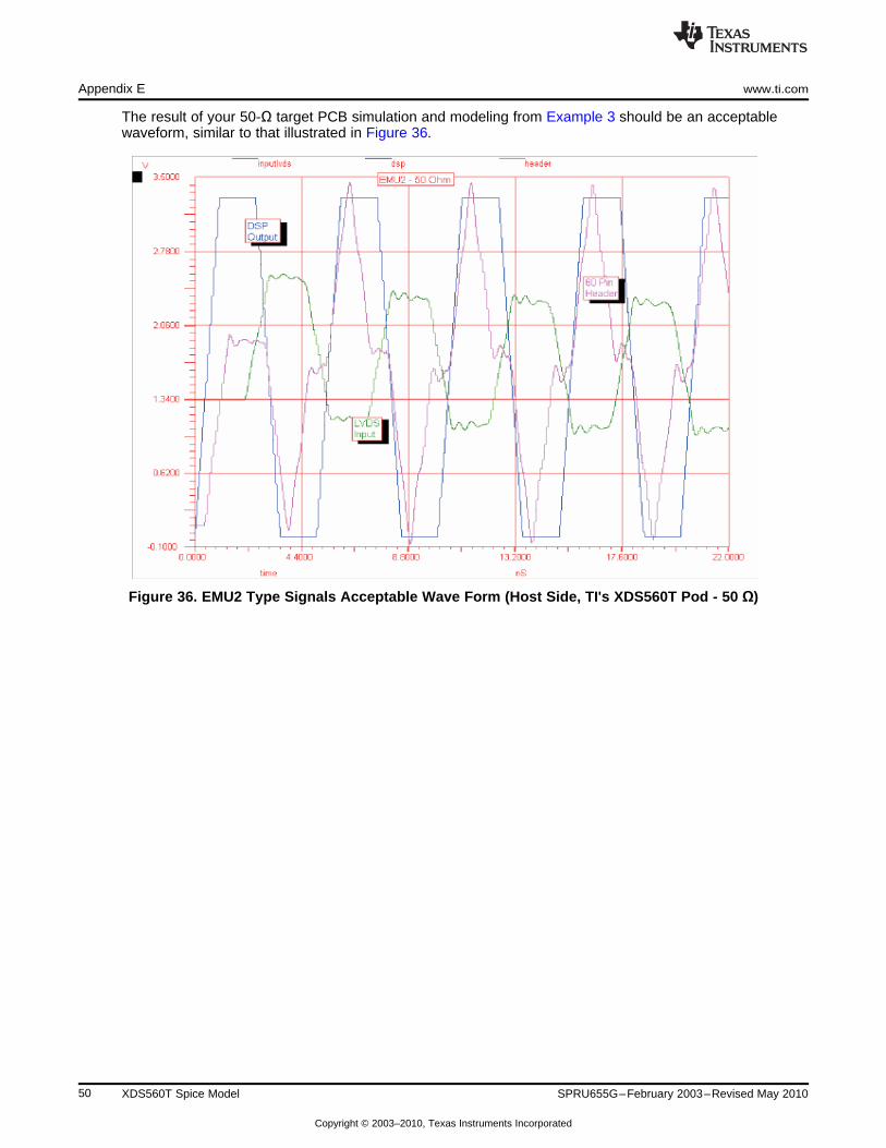
Appendix E www.ti.com
The result of your 50-Ω target PCB simulation and modeling from Example 3 should be an acceptablewaveform, similar to that illustrated in Figure 36.
Figure 36. EMU2 Type Signals Acceptable Wave Form (Host Side, TI's XDS560T Pod - 50 Ω)
50 XDS560T Spice Model SPRU655G–February 2003–Revised May 2010
Copyright © 2003–2010, Texas Instruments Incorporated

Tran0
+ V1
DSP
0.5”C0
0.5 p
Via R1
42
0.5 p
Via
C1
Tran1
1.5”
DSP totermination
Terminationto header
Seriesresistor
1 p
C2
Header N-Fheader
Tran2
0.5”
Totermination
0.5 p
Via
C4
Tran3
5.625”
Cableassembly
Tran4
0.40”
Trace
0.2”Trace-via
Tran5
0.5
p
C7
1.3
p
C14
2.87 KR309
ESD diode
+3.3 V
TREF_buffer
1.5 KR308
6 p
C11
LVDS
100 K R8
InputLVDS
0.5 pC10
1.5 KR307
C53
0.6
p C203.9 p
V2
Via
DSP - header
XDS560T EMU18
Pod header
DSP signal output60-pin headerinput to LVDS
0.5
p
C120.1”
Tran6
Termination
Via
1.5 KR310
Via
Via
www.ti.com Appendix E
Figure 37 is a representative spice model for TI's XDS560T pod assembly. Clock speeds are 200 MHz.This illustration supports a 50-Ω character-impedance target PCB. Constraints to consider or modify aretrace length and board supporting logic. Additional modeling should be done for signal cross talk.
Figure 37. EMU18 Type Signals Simulation Model (TI's XDS560T Pod Assembly - 50-Ω Target and PodModel)
51SPRU655G–February 2003–Revised May 2010 XDS560T Spice Model
Copyright © 2003–2010, Texas Instruments Incorporated

Appendix E www.ti.com
Example 4 represents the spice net list used to create the spice model in Figure 37 for a 50-Ω targetboard impedance and TI's XDS560T pod.
Example 4. EMU18 Type Signals Spice Net List (Host Side, TI's XDS560T Pod - 50 Ω)
*** Top Level Netlist ***C4 0 10 0.5pC70 6 InputLVDS 3.9pV1 DSP 0 DC 3.3V AC 0 0 PULSE 0 3.3V 0 1.00n 1.00n 1.50n 5.00nTran0 1 0 DSP 0 ZO=50 TD=.088ns F=200Meg NL=0.5Tran1 Header 0 9 0 ZO=50 TD=.264ns F=200Meg NL=1.5Tran2 10 0 Header 0 ZO=50 TD=.176ns F=200Meg NL=0.5Tran3 10 0 13 0 ZO=50 TD=0.990ns F=200Meg NL=5.625Tran5 18 0 8 0 ZO=50 TD=0.0528n F=200Meg NL=0.2"C2 0 Header 1pC7 0 18 0.5pV2 7 0 DC 3.30 AC 0 0C0 0 1 0.5pC1 0 9 0.5pC10 0 InputLVDS 0.5pC11 0 InputLVDS 5pC12 0 8 0.5pTran6 6 0 18 0 ZO=50 TD=0.0176ns F=200Meg NL=0.1C14 0 6 1.3pTran4 13 0 8 0 ZO=50 TD=0.0704ns F=200Meg NL=0.4R1 1 9 42R309 InputLVDS 6 2.87KR310 7 InputLVDS 1.5KR308 7 6 1.5KR8 InputLVDS 0 100KC53 0 InputLVDS 0.5pR307 InputLVDS 0 1.5K
***** Spice models and macro models *****
***** End of spice models and macro models *****
.tran 2n 100n 0.0 2n
.save all
.end
52 XDS560T Spice Model SPRU655G–February 2003–Revised May 2010
Copyright © 2003–2010, Texas Instruments Incorporated

www.ti.com Appendix E
The result of your 50-Ω target PCB simulation and modeling from Figure 37 should be an acceptablewaveform, similar to that illustrated in Figure 38.
Figure 38. EMU18 Type Signals - Acceptable Wave Form (Host Side, TI's XDS560T Pod - 50 Ω)
53SPRU655G–February 2003–Revised May 2010 XDS560T Spice Model
Copyright © 2003–2010, Texas Instruments Incorporated

Tran0
+ V1
DSP
0.5”C0
0.5 p
Via R1
42
0.5 p
Via
C1
Tran1
1.5”
DSP totermination
Terminationto header
Seriesresistor
1 p
C2
Header 14
Tran2
0.5”
TerminationPCB
0.5 p
Via C4
Tran3
5.625”
Cableassembly
Tran4
0.576”
Trace
0.6”Trace
Tran5
0.5
p
C7
1.3
p
C14
ESD diode
+
3.3 VTREF_buffer
1.5 KR215
6 p
C11
LVDS
100 K R8
InputLVDS
0.5 pC10
1.5 KR214
C9
0.5
p
C503.9 p
V2
Via
DSP - header
XDS560T dual header (14 & 60) EMU0
Pod header
Probe pointsDSP signal output14-pin headerinput to LVDS
1.3658”trace-via
Tran6
Resistor U23
1.5 KR217
Via
Via
Tran8
0.5
p
C51
C52
1 p R300
100 K
SeriesTarget pod
header
Trans to14-pin header
0.5
p
Via
C12
C133 p
R100 100 K
2.87 KR215
R21827
C54 p
R3 100 K
ESDtermination
Tran7
0.7”
Appendix E www.ti.com
Figure 39 is a spice model for a dual-header configuration using TI's XDS560T pod assembly. Clockspeeds are 200 MHz. This illustration supports a 50-Ω character-impedance target PCB. Dual-headerconfigurations are not recommended and require a variety of constraints to be modeled (trace length andsupporting logic). Additional modeling should be done for signal cross talk.
It is strongly recommended that only TI's emulation header be used.
Figure 39. EMU0 Dual-Header Simulation Model (TI's XDS560T Pod Assembly - 50-Ω Target and PodModel)
54 XDS560T Spice Model SPRU655G–February 2003–Revised May 2010
Copyright © 2003–2010, Texas Instruments Incorporated

www.ti.com Appendix E
Example 5 represents the spice net list used to create the spice model in Figure 39 for a 50-Ωdual-header target board impedance and TI's XDS560T pod.
Example 5. EMU0 Dual-Header Spice Net List (Host Side, TI's XDS560T Pod - 50 Ω)
*** Top Level Netlist ***C4 0 10 0.5pC50 12 InputLVDS 3.9pV1 DSP 0 DC 3.3V AC 0 0 PULSE 0 3.3V 0 800.00p 800.00p 2.20n 4.40nTran0 1 0 DSP 0 ZO=50 TD=.088ns F=200Meg NL=0.5Tran1 5 0 9 0 ZO=50 TD=.264ns F=200Meg NL=1.5Tran2 10 0 5 0 ZO=50 TD=.176ns F=200Meg NL=0.5Tran3 10 0 13 0 ZO=50 TD=0.990ns F=200Meg NL=5.625Tran6 2 0 18 0 ZO=50 TD=0.2403808ns F=200Meg NL=1.3658C2 0 5 1pC7 2 0 0.5pC6 8 0 4pV2 16 0 DC 3.30 AC 0 0C9 0 InputLVDS 0.5pC0 0 1 0.5pC1 0 9 0.5pC10 0 InputLVDS 0.5pC11 0 InputLVDS 5pC12 13 0 0.5pTran5 14 0 18 0 ZO=50 TD=.1056ns F=200Meg NL=0.6Tran7 12 0 2 0 ZO=50 TD=0.1232ns F=200Meg NL=0.7C13 0 2 3pC14 0 2 1.3pTran4 13 0 18 0 ZO=50 TD=0.176ns F=200Meg NL=0.576R1 1 9 42R216 InputLVDS 12 2.87KR217 16 InputLVDS 1.5KR215 16 12 1.5KR100 2 0 100KR3 8 0 100KR218 8 14 27R214 InputLVDS 0 1.5KR8 InputLVDS 0 100KTran8 5 0 Header14 0 ZO=50 TD=0.2816ns F=200Meg NL=1.6C51 0 5 0.5pC52 0 Header14 1pR300 Header14 0 100K
***** Spice models and macro models *****
***** End of spice models and macro models *****
.tran 1n 100n 0.0 1n
.save all
.end
55SPRU655G–February 2003–Revised May 2010 XDS560T Spice Model
Copyright © 2003–2010, Texas Instruments Incorporated

Appendix E www.ti.com
The result of your 50-Ω dual-header target PCB simulation and modeling from Figure 39 should be anacceptable waveform, similar to that illustrated in Figure 40.
Figure 40. EMU0 Dual-Header - Wave Form (Host Side, TI's XDS560T Pod - 50 Ω)
56 XDS560T Spice Model SPRU655G–February 2003–Revised May 2010
Copyright © 2003–2010, Texas Instruments Incorporated

www.ti.com
Appendix F XDS560 v2 System Trace Modeling
Figure 41 shows the TRCLK[0] model schematic. SLM_qth01_qsh01 in the model represents thecombination of the emulation header on the target card and the target cable connector. For the mostaccurate simulation, TI recommends using tools that support simulation with IBIS models of your targetdevice (U11.1 in Figure 41) and the AVC4T245_RGY buffer.
57SPRU655G–February 2003–Revised May 2010 XDS560 v2 System Trace Modeling
Copyright © 2003–2010, Texas Instruments Incorporated
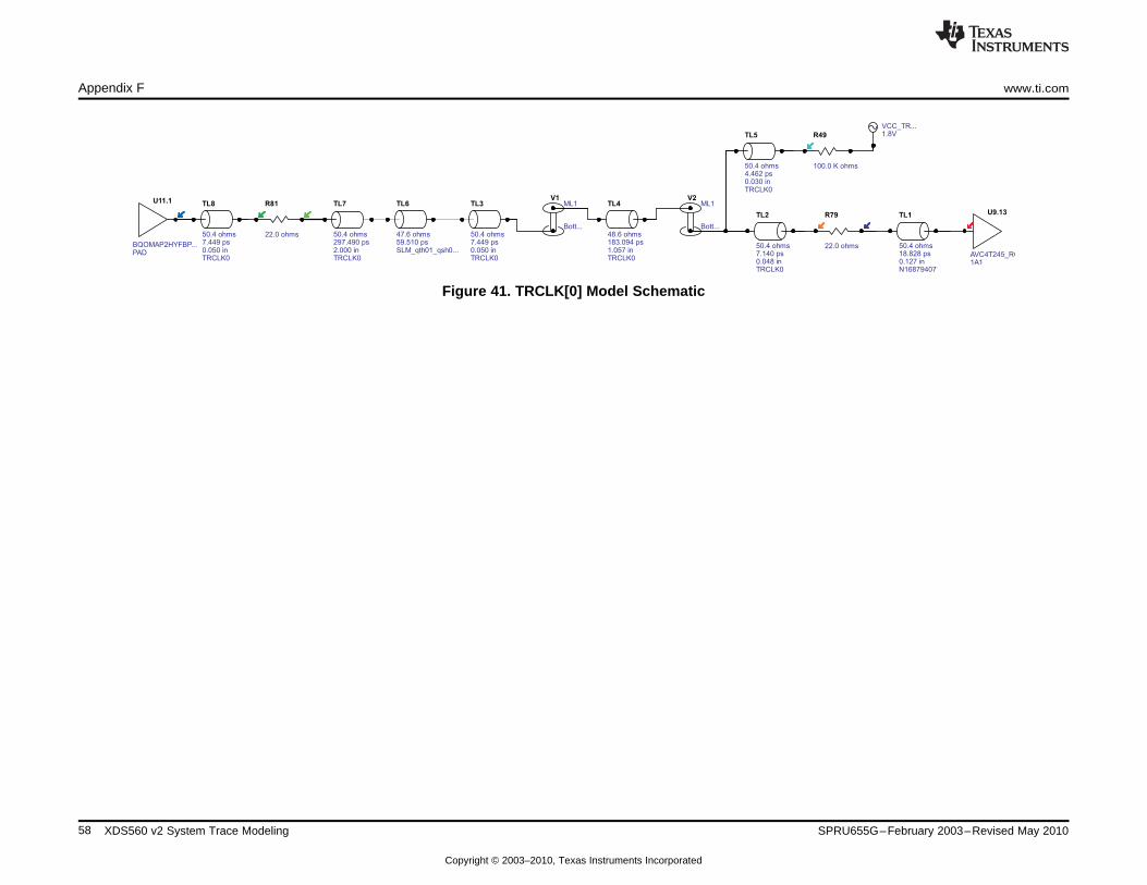
U9.13
AVC4T245_RGY1A1
TL1
50.4 ohms18.828 ps0.127 inN16879407
R79
22.0 ohms
TL2
50.4 ohms7.140 ps0.048 inTRCLK0
TL6
47.6 ohms59.510 psSLM_qth01_qsh0...
TL3
50.4 ohms7.449 ps0.050 inTRCLK0
V1ML1
Bott...
TL4
48.6 ohms183.094 ps1.057 inTRCLK0
V2ML1
Bott...
TL5
50.4 ohms4.462 ps0.030 inTRCLK0
R49
100.0 K ohms
VCC_TR...1.8V
R81
22.0 ohms
TL7
50.4 ohms297.490 ps2.000 inTRCLK0
TL8
50.4 ohms7.449 ps0.050 inTRCLK0
U11.1
BQOMAP2HYFBP...PAD
Appendix F www.ti.com
Figure 41. TRCLK[0] Model Schematic
58 XDS560 v2 System Trace Modeling SPRU655G–February 2003–Revised May 2010
Copyright © 2003–2010, Texas Instruments Incorporated

www.ti.com
Appendix G Finding a Buffer's Output Impedance
To determine the nominal impedance of a device's JTAG or EMU pin output buffer, reference the IBISmodel for the device. Find the "model_name" of the pin's buffer using the name of the pin as defined inthe device's data sheet (i.e., EMU0, TCK) and use the key from Table 27 to decode the name anddetermine the output impedance of the buffer. Table 28 provides a list of common buffers and therecommended series termination resistor value. In some cases, a shorthand version of the model_name isused. In this case, you must find the definition of the buffer in the IBIS file and look for the componentcomment (for an example, see Table 29).
Table 27. Buffer Name Decode andOutput Impedance
Buffer Name: BT 3325 ET HYPU FZSC P18
B Driver/Receiver (O = Output).
T TTL © = CMOS).
33 Supply voltage; i.e., 3.3 V.
25 Nominal impedance; i.e., 25 Ω.
E Buffer's design frequency; i.e., 250 MHz.
A = 50 MHz
B = 100 MHz
C = 150 MHz
D = 200 MHz
E = 250 MHz
F = 300 MHz
Table 28. Recommended Series Termination Resistor Value
Recommended TerminationBuffer Types (1) Output Impedance Resistor
BT3315DTHYPU 15 33
BT3325ETPU 25 24
BT3325ETHYPUFZSCP18 25 24
BC1825ETHYPUFZ 25 24
BC1825ESHYPUFZ 25 24
IDH04_UOT335_PS100 (2) 42(1) Do not assume that all EMU and JTAG pins use the same buffers. Fore example, a TMS320C6457
uses a BC1825ETHYPUFZ for all the EMU pins, but the TDO pin uses a BC1840ETHYFZ. In this case,the EMU pins require 24-Ω series termination resistors, while TDO requires a much smaller, 10-Ω,termination resistor.
(2) In some early trace supported devices, the IBIS buffer naming convention was not used. If you findcases other than IDH04_UOT335_PS100, we recommend you contact your TI field servicerepresentative to get the buffer output impedance.
59SPRU655G–February 2003–Revised May 2010 Finding a Buffer's Output Impedance
Copyright © 2003–2010, Texas Instruments Incorporated

Appendix G www.ti.com
Table 29. Model_name Example
Pin Signal_name Model_name R_pin L_pin C_pin
H23 TCK KP18PUSR50 1.14E+00 2.78E-09 1.62E-12
J22 TDI THYPUFZP18 1.10E+00 2.58E-09 1.66E-12
J23 TDO EPUFZSCP18 1.16E+00 2.67E-09 1.47E-12
L22 TMS THYPUFZP18 9.03E-01 2.34E-09 1.52E-12
L23 TRST THYPDFZP18 1.03E+00 2.62E-09 1.41E-12
K23 EMU0 EPUFZSCP18 1.08E+00 2.62E-09 1.49E-12
K22 EMU1 EPUFZSCP18 1.02E+00 2.47E-09 1.58E-12
K21 EMU2 EPUFZSCP18 7.51E-01 2.07E-09 1.39E-12
K20 EMU3 EPUFZSCP18 5.34E-01 1.66E-09 1.26E-12
L18 EMU4 EPUFZSCP18 2.72E-01 1.21E-09 1.07E-12
J21 EMU5 EPUFZSCP18 8.00E-01 2.22E-09 1.48E-12
K19 EMU6 EPUFZSCP18 4.11E-01 1.49E-09 1.19E-12
H21 EMU7 EPUFZSCP18 9.35E-01 2.47E-09 1.51E-12
J20 EMU8 EPUFZSCP18 6.07E-01 1.77E-09 1.33E-12
H20 EMU9 EPUFZSCP18 6.51E-01 1.98E-09 1.35E-12
J19 EMU10 EPUFZSCP18 4.39E-01 1.54E-09 1.18E-12
K18 EMU11 EPUFZSCP18 1.61E-01 1.32E-09 9.70E-13
In the case of TDO, you must search the IBIS model for the following comment:|*******************************************************************************|| Component BT3325ETHYPUFZSCP18 -May 28, 2007 Rev 1.1| Note: Shortened Model name is EPUFZSCP18|*******************************************************************************
60 Finding a Buffer's Output Impedance SPRU655G–February 2003–Revised May 2010
Copyright © 2003–2010, Texas Instruments Incorporated
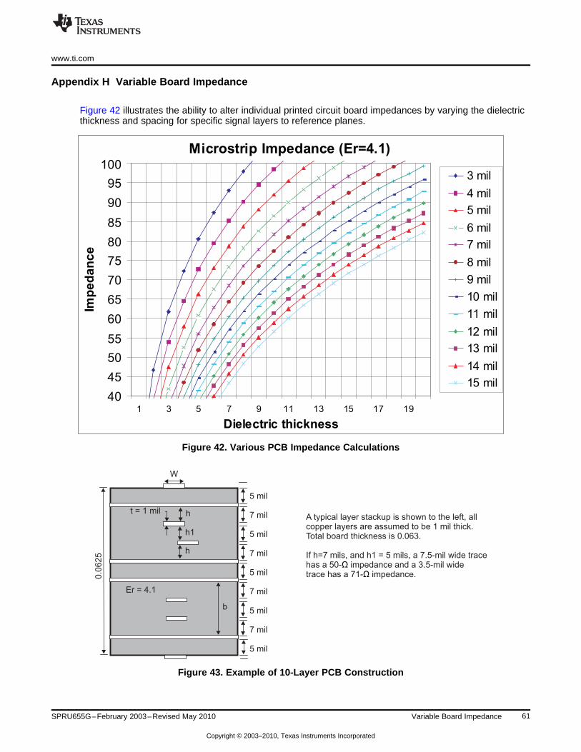
Microstrip Impedance (Er=4.1)
40
45
50
55
60
65
70
75
80
85
90
95
100
1 3 5 7 9 11 13 15 17 19
Dielectric thickness
Imp
ed
an
ce
3 mil
4 mil
5 mil
6 mil
7 mil
8 mil
9 mil
10 mil
11 mil
12 mil
13 mil
14 mil
15 mil
5 mil
7 mil
5 mil
7 mil
5 mil
7 mil
5 mil
7 mil
5 mil
A typical layer stackup is shown to the left, allcopper layers are assumed to be 1 mil thick.Total board thickness is 0.063.
If h=7 mils, and h1 = 5 mils, a 7.5-mil wide tracehas a 50- impedance and a 3.5-mil widetrace has a 71- impedance.
ΩΩ
W
t = 1 mil h
h1
h
b
Er = 4.1
0.0
625
www.ti.com
Appendix H Variable Board Impedance
Figure 42 illustrates the ability to alter individual printed circuit board impedances by varying the dielectricthickness and spacing for specific signal layers to reference planes.
Figure 42. Various PCB Impedance Calculations
Figure 43. Example of 10-Layer PCB Construction
61SPRU655G–February 2003–Revised May 2010 Variable Board Impedance
Copyright © 2003–2010, Texas Instruments Incorporated

www.ti.com
Appendix I Revision History
This revision history highlights the technical changes made to the document in revision D.
Table 30. Emulation and Trace Headers Revision History
See Additions/Modifications/Deletions
Table 12 Added Footnote (1) to TDIS signal
62 Revision History SPRU655G–February 2003–Revised May 2010
Copyright © 2003–2010, Texas Instruments Incorporated
IMPORTANT NOTICE
Texas Instruments Incorporated and its subsidiaries (TI) reserve the right to make corrections, modifications, enhancements, improvements,and other changes to its products and services at any time and to discontinue any product or service without notice. Customers shouldobtain the latest relevant information before placing orders and should verify that such information is current and complete. All products aresold subject to TI’s terms and conditions of sale supplied at the time of order acknowledgment.
TI warrants performance of its hardware products to the specifications applicable at the time of sale in accordance with TI’s standardwarranty. Testing and other quality control techniques are used to the extent TI deems necessary to support this warranty. Except wheremandated by government requirements, testing of all parameters of each product is not necessarily performed.
TI assumes no liability for applications assistance or customer product design. Customers are responsible for their products andapplications using TI components. To minimize the risks associated with customer products and applications, customers should provideadequate design and operating safeguards.
TI does not warrant or represent that any license, either express or implied, is granted under any TI patent right, copyright, mask work right,or other TI intellectual property right relating to any combination, machine, or process in which TI products or services are used. Informationpublished by TI regarding third-party products or services does not constitute a license from TI to use such products or services or awarranty or endorsement thereof. Use of such information may require a license from a third party under the patents or other intellectualproperty of the third party, or a license from TI under the patents or other intellectual property of TI.
Reproduction of TI information in TI data books or data sheets is permissible only if reproduction is without alteration and is accompaniedby all associated warranties, conditions, limitations, and notices. Reproduction of this information with alteration is an unfair and deceptivebusiness practice. TI is not responsible or liable for such altered documentation. Information of third parties may be subject to additionalrestrictions.
Resale of TI products or services with statements different from or beyond the parameters stated by TI for that product or service voids allexpress and any implied warranties for the associated TI product or service and is an unfair and deceptive business practice. TI is notresponsible or liable for any such statements.
TI products are not authorized for use in safety-critical applications (such as life support) where a failure of the TI product would reasonablybe expected to cause severe personal injury or death, unless officers of the parties have executed an agreement specifically governingsuch use. Buyers represent that they have all necessary expertise in the safety and regulatory ramifications of their applications, andacknowledge and agree that they are solely responsible for all legal, regulatory and safety-related requirements concerning their productsand any use of TI products in such safety-critical applications, notwithstanding any applications-related information or support that may beprovided by TI. Further, Buyers must fully indemnify TI and its representatives against any damages arising out of the use of TI products insuch safety-critical applications.
TI products are neither designed nor intended for use in military/aerospace applications or environments unless the TI products arespecifically designated by TI as military-grade or "enhanced plastic." Only products designated by TI as military-grade meet militaryspecifications. Buyers acknowledge and agree that any such use of TI products which TI has not designated as military-grade is solely atthe Buyer's risk, and that they are solely responsible for compliance with all legal and regulatory requirements in connection with such use.
TI products are neither designed nor intended for use in automotive applications or environments unless the specific TI products aredesignated by TI as compliant with ISO/TS 16949 requirements. Buyers acknowledge and agree that, if they use any non-designatedproducts in automotive applications, TI will not be responsible for any failure to meet such requirements.
Following are URLs where you can obtain information on other Texas Instruments products and application solutions:
Products Applications
Amplifiers amplifier.ti.com Audio www.ti.com/audio
Data Converters dataconverter.ti.com Automotive www.ti.com/automotive
DLP® Products www.dlp.com Communications and www.ti.com/communicationsTelecom
DSP dsp.ti.com Computers and www.ti.com/computersPeripherals
Clocks and Timers www.ti.com/clocks Consumer Electronics www.ti.com/consumer-apps
Interface interface.ti.com Energy www.ti.com/energy
Logic logic.ti.com Industrial www.ti.com/industrial
Power Mgmt power.ti.com Medical www.ti.com/medical
Microcontrollers microcontroller.ti.com Security www.ti.com/security
RFID www.ti-rfid.com Space, Avionics & www.ti.com/space-avionics-defenseDefense
RF/IF and ZigBee® Solutions www.ti.com/lprf Video and Imaging www.ti.com/video
Wireless www.ti.com/wireless-apps
Mailing Address: Texas Instruments, Post Office Box 655303, Dallas, Texas 75265Copyright © 2010, Texas Instruments Incorporated
![Apple ][ Emulation on an AVR Microcontroller Emulation ... · Apple ][ Emulation on an AVR Microcontroller Emulation eines Apple ][ auf einem AVR Mikrocontroller Maximilian Strauch](https://img.pdfslide.net/doc/110x75/5d494b4588c99334058bd1f6/apple-emulation-on-an-avr-microcontroller-emulation-apple-emulation.jpg)